Figure (7-8)
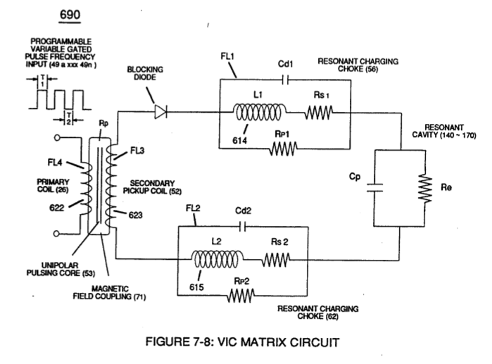
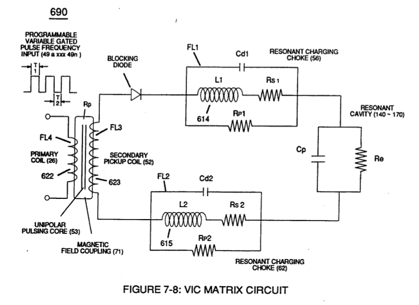
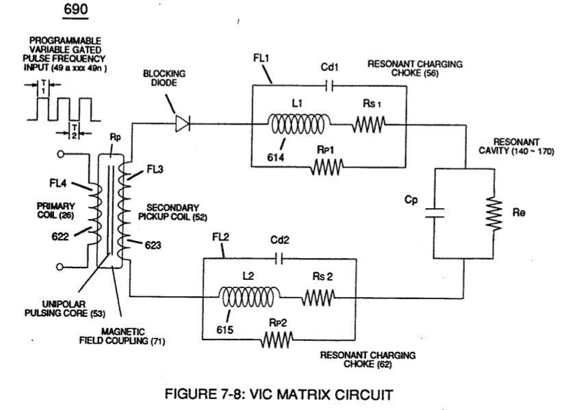
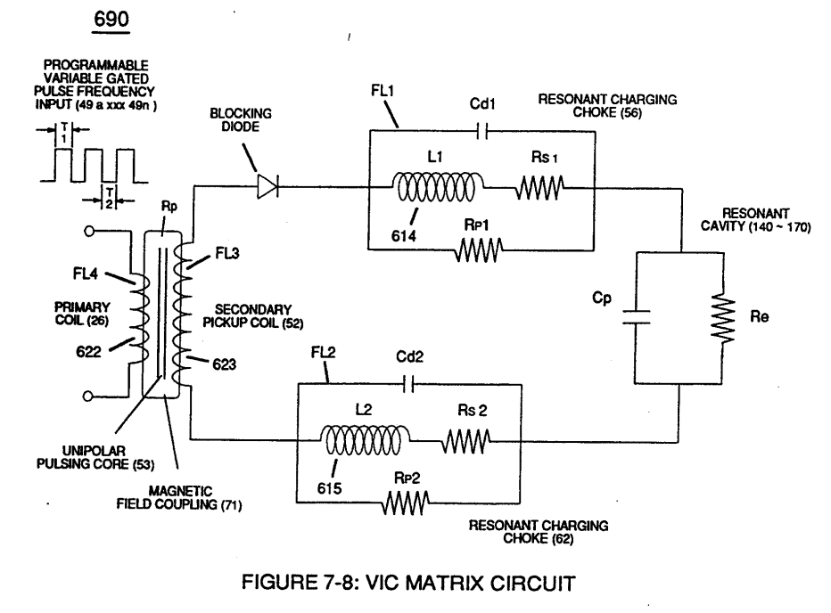
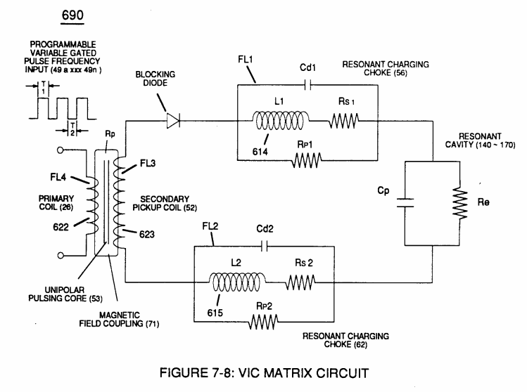
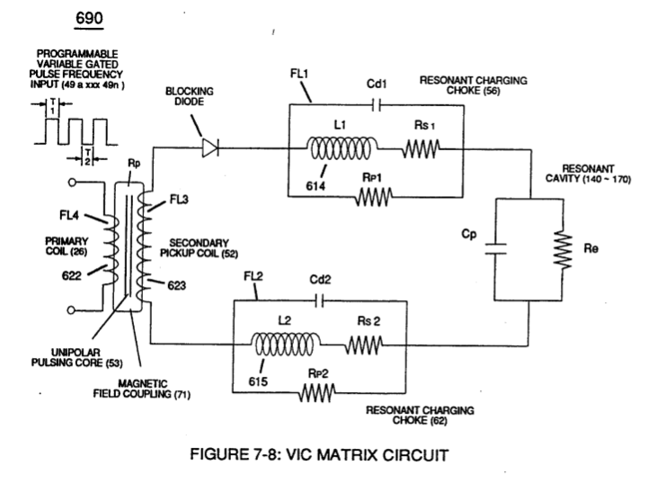
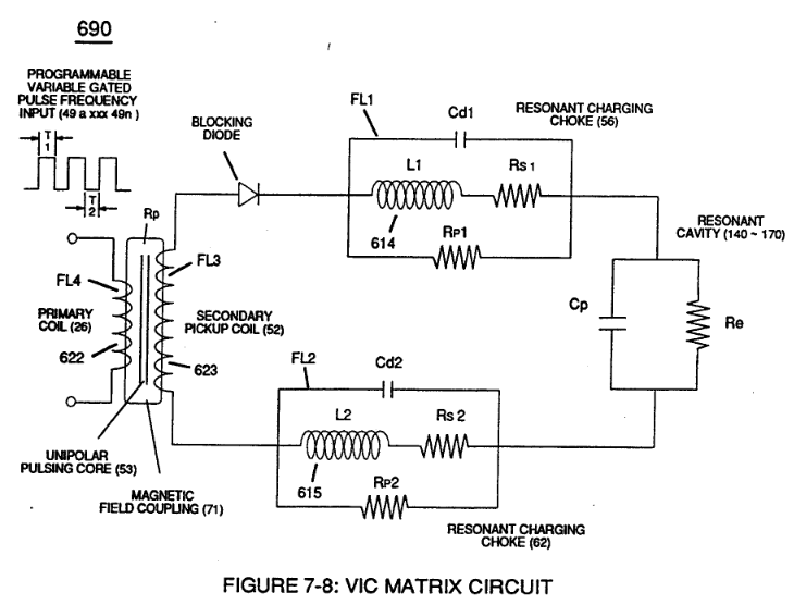
VIC Matrix Circuit
Also written End Plate Hi-temperature Quarts Tube
How it is written
- (7-8) 70×
Drawings 18
-
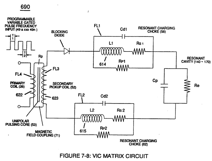
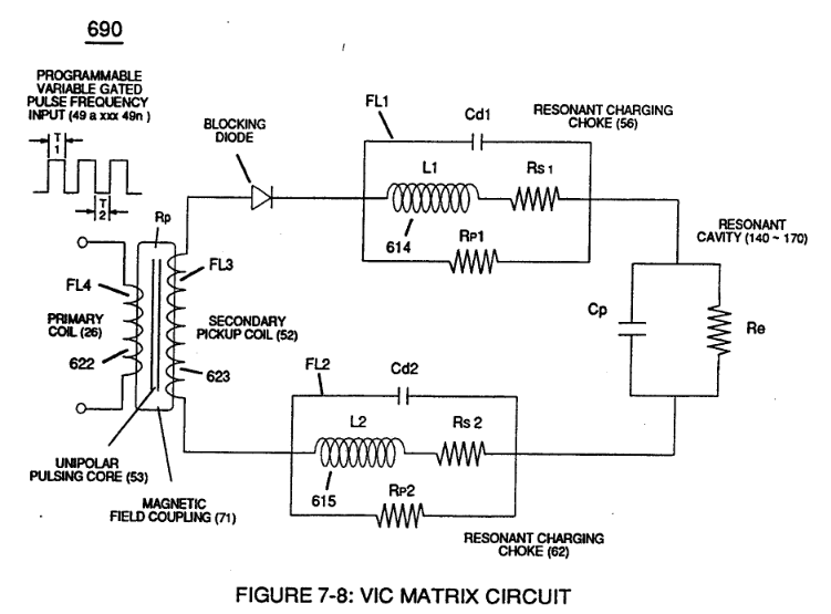
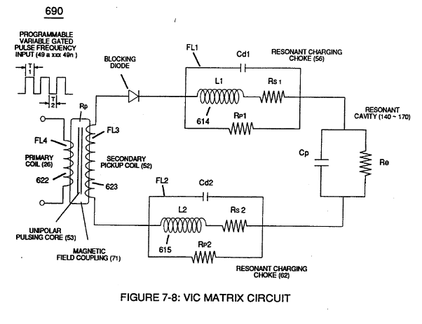
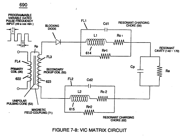
Captioned as this figure · VIC Matrix Circuit
-
(T2) of Figure (7-8) · Instant Explosion of Water
-
Figure (7-8) · Resistance (Rs)
-
(690) of Figure (7-8) · Resistance (Rs)
-
(690) of Figure (7-8) · Inductance (FL)
-
(690) of Figure (7-8) · Capacitance (Cd)
-
(690) of Figure (7-8) · Inductance Reactance (Rs - Cd - FL)
-
Figure (7-8) · Inductance Reactance (Rs - Cd - FL)
-
(690) of Figure (7-8) · Taper Resonant Capacitor (ERt)
-
690 of Figure 7-8 · Circuit Resistance
-
(52) of Figure (7-8) · Electron Bounce Phenomenon
-
(690) of Figure (7-8) · 8-2 - Traveling Voltage Wave-Guides
-
(52) of Figure (7-8) · 8-3 - Electrical Voltage-Pulse Wave-Transmission
-
(Cp) of Figure (7-8) · 8-4 - State Space (Sp)
-
(690) of Figure (7-8) · 8-6 - VIC Voltage Sync-Pulse Circuit
-
(Cp) of (7-8) · 8-6 - VIC Voltage Sync-Pulse Circuit
-
(690) of Figure (7-8) · Propagating Electrical Stress
-
Captioned as this figure · WFC 429 - Illustrations
On this figure 54
- 26 Primary Coil
- 49 Voltage Pulse frequency
- 52 Secondary Coil
- 53 Pulsing Core
- 55 Switching Diode
- 56 Resonant Charging Choke
- 62 Resonant Charging Chokes
- 64 Pulse Train
- 66 Positive Voltage Potential
- 67 Opposite Polarity
- 71 Magnetic Field Coupling
- 85 Water Molecule
- 542 Sub-Particle
- 614 Inductor
- 615 Resonant Charging Chokes
- 616A Dual Bifilar Secondary Pickup Coils
- 616B Dual Bifilar Secondary Pickup Coils
- 617 Molecular Polarization Alignment
- 618 Blocking Diode
- 628 Capacitance Charging Effect
- 643 —
- 690 VIC Matrix Circuit
- 860 Amp Inhibitor Circuit
- 916 Partially Transparent End Plate
- Cd Distributed Capacitance
- Cp Water Gap
- E1 Voltage Zones
- E2 Voltage Zones
- E9 Capacitor
- E10 Capacitor
- EbP Electron Bounce Phenomenon
- Eo Permittivity
- FL Optimize The Electromagnetic Field Strength
- FL1 Distributed Inductance
- FL2 Distributed Inductance
- L1 Inductor
- Re Water
- Rl Resistive Wire-Coil
- Rp Transformer Magnetic Field
- Rp1 Coupling Inductance
- Rp2 Mutual Inductance Fields
- Rpl Mutual Inductance Fields
- Rs Series Resistance Value
- Rs1 Voltage Coefficient of Resistance
- Rs2 Voltage Coefficient of Resistance
- SS56 Resonant Charging Chokes Stages
- T1 Duty Cycle of Pulse Train
- T2 Duty Cycle of Pulse Train
- Tl —
- V Voltage Amplitude
- Vn2 —
- Vsp Voltage-Sync Pulse
- Z2 Resonant Choke Coils Electromagnetic Fields Intensity
- Z3 Resonant Choke Coils Electromagnetic Fields Intensity
Where it is named · 70
Instant Explosion of Water 2×
-
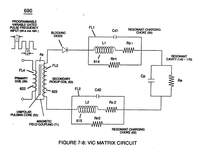
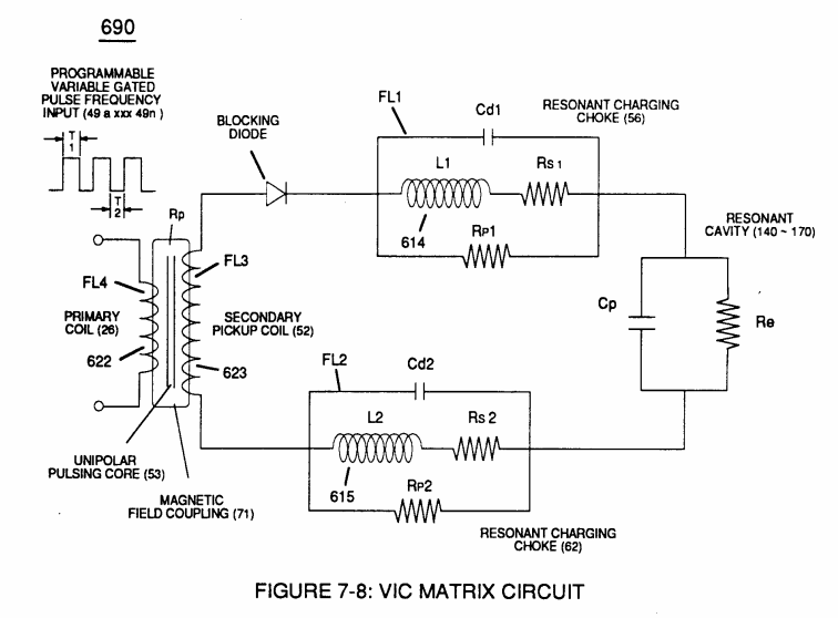
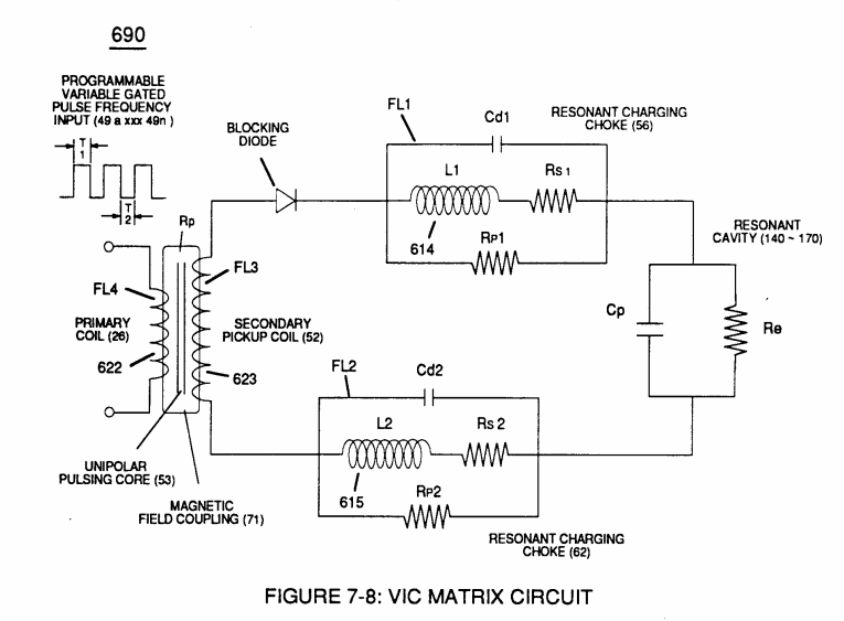
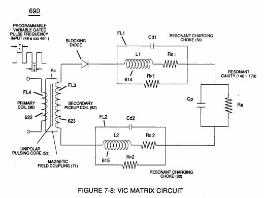
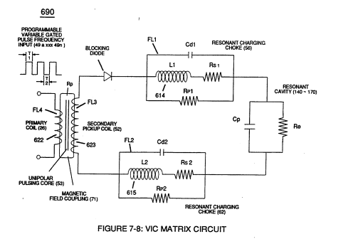
... Diode (55) being placed between Secondary Pickup Coil (52) and Resonant Charging Choke (56) to act as an electronic switch in open-position during pulse off-time (T2) of Figure (7-8) while preventing electron flow in reverse direction when Inductor (L1) collapsing electromagnetic field (FL1) produces another unipolar pulse wave-form (64a - 64b).
-
(T2) of Figure (7-8)
Resistance (Rs) 4×
-
Figure (7-8)
-
(690) of Figure (7-8)
Inductance (FL) 2×
-
(690) of Figure (7-8)
Capacitance (Cd) 4×
-
The circular-spiral turns of wire (forming parallel electrical surfaces) is separated by an Insulated Dielectric Coating Material which forms a series of capacitors (Cda xxx Cdn) when magnetic flux-lines (619a xxx 619n) produce Electromagnetic Coupling Field (621) during pulse on-time (T1), as illustrated in (640) of Figure (7-3) as to (690) of Figure (7-8).
-
(690) of Figure (7-8)
-
(690) of Figure (7-8)
Inductance Reactance (Rs - Cd - FL) 9×
-
Inductance Reactance occurs when resistance (Rs), capacitance (Cd), and Inductance (FL) interacts together during D.C. Pulsing (49a xxx 49n), as schematically depicted in (690) of Figure (7-8).
-
(690) of Figure (7-8)
-
(Cp) of Figure (7-8)
-
At elevated or higher amplitude voltage levels (xxx Ve xxx Vf xxx Vn), primary electromagnetic coupling field (Rp) of Figure (7-8) transmitted by way of Inductance Pulsing-Core (190) of Figure (3-23) as to VIC Coil Assembly (580) of Figure (6-1) enters into and passes through both Inductors (L1/L2) simultaneously and offers not …
-
(Rp) of Figure (7-8)
-
... paralleling and performing the same electromagnetic characteristic of copper wire when it comes to magnetic field reformation (Rp - Rp 1 - Rp2) of Figure (7-8), as further illustrated in electromagnetic coupling fields (71 - 511 - 512) of Figure (6-1) that encourages, brings-on, and perform Voltage Inducement Process (580) of Figure (6-1) as to (620) of Fig …
-
Figure (7-8)
Taper Resonant Capacitor (ERt) 3×
-
Capacitance (Cp) of Figure (7-6) as to (690) of Figure (7-8) is determined by the surface area (A) of Electrical Voltage-Plates (E1/E2 - E9/E10), the distance (d) between the Electrical Plates (in inches), and the permittivity (Eo) of the dielectric property of water (85) and, is expressed in the following equation:
-
(690) of Figure (7-8)
Capacitance Reactance 2×
-
(690) of Figure (7-8)
Circuit Resistance 4×
-
(52) of Figure (7-8)
-
690 of Figure 7-8
Transformer Action 10×
-
Inductance Core (53) of Figure (6-1) composed of "Grain Oriented" Electrical Steel laminations step up applied Voltage (49) when Magnetic Field Coupling (71) of Figure (7-8) cross over to Secondary Pickup Coil-winding (52) which has more turns of wire than Primary Coil- winding (26) by way of "Eddy" currents that induce magnetic flux lines of forces (71a xxx 71n) emanati …
-
… es (71a xxx 71n) emanating away from magnetic core material (53) and caused by Primary Coil (26) being electrically energized during pulsing operations (T1a xx T1n), as illustrated in (690) of Figure (7-8).
-
(71) of Figure (7-8)
-
(690) of Figure (7-8)
-
… e "Electron Clustering" (Grouping/collecting negative charged particles at a given point) (700) of Figure (7-9) to produce ''Negative Voltage Potential" ( B- ) at one side of Water Gap (Cp) of Figure (7-8) is accomplished by low electrical power input (Tab 38) when Choke-Coil (62) of Figure (7-1) magnetic field (FL2) (690) of Figure (7-8) during pulse on-time (49) impede "Electron-Flow" since electron …
-
… oltage Potential" ( B- ) at one side of Water Gap (Cp) of Figure (7-8) is accomplished by low electrical power input (Tab 38) when Choke-Coil (62) of Figure (7-1) magnetic field (FL2) (690) of Figure (7-8) during pulse on-time (49) impede "Electron-Flow" since electron mass is composed of electromagnetic matter which interacts with magnetic field strength (FL2).
Electron Bounce Phenomenon 3×
-
Magnetic Field Coupling (71) of Figure (7-9) entering into and passing through Secondary Coil-winding (52) of Figure (7-8) causes and produces copper ions (643a xxx 643n) (Positive Charged atoms 542a xxx 542n having missing electrons) when moving external electromagnetic field strength (71a xxx 71n) is sufficient enough …
-
(52) of Figure (7-8)
Mode of Operability 1×
-
Pulse Off-time (T2) of Figure (7-8) as to (620) of Figure (7-1) is adjusted to compensate for the rise and fall of magnetic coupling field (71) to produce applied Unipolar Wave-forms (64a xxx 64n) entering into Wave-guides (35a/35b/35c).
8-2 - Traveling Voltage Wave-Guides 5×
-
The dielectric property of water (85) (resistance to electron flow) in conjunction with VIC Coil Matrix Circuit (690) of Figure (7-8) (WFC memo 426) as to VIC Coil Assembly (580) of Figure (6-1) (WFC memo 425) ability to inhibit amp "influxing" (Electron Bounce Phenomenon EbP) during pulsing operations (49a xx 49n) allows voltage a …
-
(690) of Figure (7-8) (WFC memo 426)
-
Voltage Intensifier Matrix Circuit (690) of Figure (7-8) electrically connected with resistive liquid (85/Re) (forming Resonant Water Gap "Cp" of Figure 7-8) propagates the transmission of Traveling Voltage Wave-Form (57) of Figure (6-2) as to (770) of Figure(8-1) by the functional relationship of Circuit Resistance Equation (Eq 9) during programmable Voltage Pulsing operations (49a xxx 1'3 xxx 49n) of Figure (8-2).
-
Voltage Intensifier Matrix Circuit (690) of Figure (7-8) electrically connected with resistive liquid (85/Re) (forming Resonant Water Gap "Cp" of Figure 7-8) propagates the transmission of Traveling Voltage Wave-Form (57) of Figure (6-2) as to (770) of Figure(8-1) by the functional relationship of Circuit Resistance Equation (Eq 9) during programmable Voltage Pulsing operations (49a xxx 1'3 xxx 49n) of Figure (8-2).
-
(690) of Figure (7-8)
8-3 - Electrical Voltage-Pulse Wave-Transmission 5×
-
The newly established leading voltage edge (Vpa) and trailing voltage edge (Vpb) being uniform in shape/configuration since both Resonant Charging Chokes (56/Z2 – 62/Z3) resistive values are the same (Typically 11.6 kΩ each) and incoming signal (49a xxx 49n) is electrically linked with Water-Gap Capacitor (Cp) of Figure (7-8) having dielectric liquid of Water (85) there between.
-
Figure (7-8)
-
(52) of Figure (7-8)
8-4 - State Space (Sp) 2×
-
During the electrical-formation (66- Vpa/Vpb - 67- Vpa/Vpb) of each opposite Electrical Voltage-Wave (66-583 - 67-602), opposite electrical attraction force (RR' - SS') of Figure (7-4) is produced across water cap (Cp) of Figure (7-8) which, now, sets up and defines the conditions of “State Space," as illustrated in (770 A/B) of Figure (8-1) as to (650) of Figure (7-4).
-
(Cp) of Figure (7-8)
8-6 - VIC Voltage Sync-Pulse Circuit 4×
-
… ting Coil 617, Blocking Diode 618, and Magnetic Induction Core 619) between electrical ground (0V) and Center Tap of Dual Bifilar Secondary Pickup Coils (616A/B) of VIC Matrix Circuit (690) of Figure (7-8) as to VIC Impedance Network Circuit (620) of Figure (7-1) , as illustrated in (840) of Figure (8-10).
-
(690) of Figure (7-8)
-
To ensure and maintain Capacitance Charging Effect (650) of Figure (7-4) across Water-Gap (Cp) of (7-8) during applied pulsing operations (49a xxx 49n), Crossover Voltage Wave-Form (780B) as to (780C) of Figure (8-2) is generally utilized by not allowing Convergent Point "Q" of Figure (780B) to reach E …
-
(Cp) of (7-8)
Propagating Electrical Stress 3×
-
(690) of Figure (7-8)
-
The energized "Resonant Charging Choke" (56) of Figure (7-1) as to Figure (10-1) by way of input voltage-pulses (49a xxx 49n) creates an electromagnetic coupling field (Rp1) of Figure (7-8) due to its self-inductance (640) of Figure 7-3B) crosses over and passes through electrically ground connected Resonant Charging Choke (62), as so illustrated in Figure (10-1)
Voltage to Amp Differential Ratio 3×
-
… ss steel coil-wire length and magnet bifilar-coil (56/62) is placed on top of Stainless Steel bifilar-coil (SS56/62) to maximize mutual inductance coil-field (Rp2) (adding Rp1+Rp2) of (690) of Figure (7-8) to cause coil capacitance (Cda xxx Cdn) to help maintain and even increase pulse voltage amplitude (xxx Vn + Vn 1 + Vn2 + Vn .... …
-
… etc.) while the resistive value (Rs2) of SS Coil-Wire (SS56/62) performs the work of further resisting the flow of amps not inhibited by both self-Inductance fields (Rpl + Rp2), as so illustrated in (690) of Figure (7-8).
-
(690) of Figure (7-8)
A Technique Called "Easer" 2×
Appendix B - Glossary of Applicaiton Notes 2×
-
… ause "Electron Clustering" (Grouping/collecting negative charged particles at a given point) (700) of Figure (7-9) to produce "Negative Voltage Potential" (B-) at one side of Water Gap (Cp) of Figure (7-8) is accomplished by low electrical power input (Tab 38) when Choke-Coil (62) of Figure (7-1) magnetic field (FL2) (690) of Figure (7-8) during pulse on-time (49) impede "Electron-Flow" since electron mass is composed of electromagnetic matter which interacts with magnetic field strength (FL2). …
-
… Voltage Potential" (B-) at one side of Water Gap (Cp) of Figure (7-8) is accomplished by low electrical power input (Tab 38) when Choke-Coil (62) of Figure (7-1) magnetic field (FL2) (690) of Figure (7-8) during pulse on-time (49) impede "Electron-Flow" since electron mass is composed of electromagnetic matter which interacts with magnetic field strength (FL2). …