(Cp)
Water Gap
Also written capacitor gap · Resonant Water Gap · Gap · Resonant Cavity · Water-Gap Capacitor · Capacitor-Gap · Capacitance · Water-Gap
Where it is first named
… ignal distortion" or "signal degradation" (preventing transformer ringing during signal propagation) as elevated voltage levels ( - xx Vc- xx Vd - xx Vn) while allowing the reduction of Capacitor-Gap (Cp) (616) of Figure (7-11) width spacing (57 of Figure 3- 25 ~35 of Figure 6-2) (typically .060 - .010) respectively as illustrated in Tubular Resonant Cavity (170) as to Taper Resonant Cavity (620) of F …
How it is written
- (Cp) 25×
Drawings 56
-
''Negative Voltage Potential" ( B- ) at one side of Water Gap (Cp) of Figure (7-8) & magnetic field (FL2) (690) of Figure (7-8) · Transformer Action
-
(Cp) of Figure (7-8) · 8-4 - State Space (Sp)
-
(Cp) of (7-8) · 8-6 - VIC Voltage Sync-Pulse Circuit
-
Figure (1-4) · LC Circuit
-
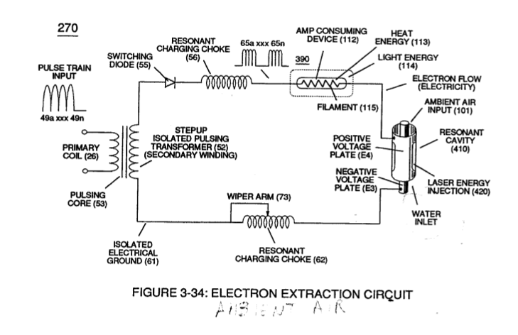
(270) of Figure (3-34) · Gas Processor
-
The figure it sits on · WFC 422DA - Illustrations
-
(80) of Figure (4) · Water Fuel Injector (Taper Resonant Cavity Chamber)
-
(650) of Figure (7-4) · Amp Inhibiting Circuit Vs Voltage Enhancement
-
(270) of (3-34) · In Application of Usage
-
The figure it sits on · VIC Matrix Circuit
-
(616) of Figure (7-11) · Instant Explosion of Water
-
(T2) of Figure (7-8) · Instant Explosion of Water
-
Figure (7-8) · Resistance (Rs)
-
(650) of Figure (7-4) · Resistance (Rs)
-
(690) of Figure (7-8) · Resistance (Rs)
-
(720) of Figure (7-11) · Inductance (FL)
-
(720, 616) of Figure (7-11) · Inductance (FL)
-
The figure it sits on · Inductance (FL)
-
(670) of Figure (7-6) · Inductance (FL)
-
(690) of Figure (7-8) · Inductance (FL)
-
Capacitor (E9/E10) of Figure (7-11) · Inductance (FL)
-
(650) of Figure (7-4) · Inductance (FL)
-
(720) of Figure (7-11) · Capacitance (Cd)
-
(650) of Figure (7-4) · Capacitance (Cd)
-
(670) of Figure (7-6) · Capacitance (Cd)
-
(670) of Figure (7-6) · Capacitance (Cd)
-
(690) of Figure (7-8) · Capacitance (Cd)
-
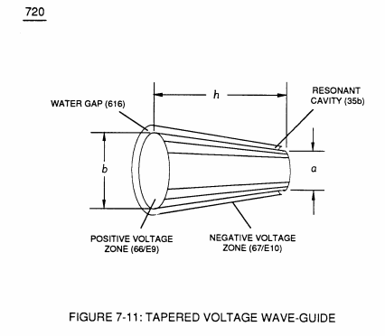
(690) of Figure (7-8) · Inductance Reactance (Rs - Cd - FL)
-
Figure (7-8) · Inductance Reactance (Rs - Cd - FL)
-
The figure it sits on · Taper Resonant Capacitor (ERt)
-
(690) of Figure (7-8) · Taper Resonant Capacitor (ERt)
-
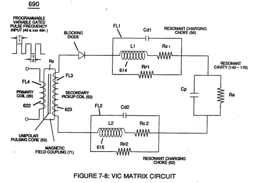
(see diagram 720 of Figure 7-11) · Taper Resonant Capacitor (ERt)
-
diagram 720 of Figure 7-11 · Taper Resonant Capacitor (ERt)
-
Resonant Capacitor (140 -170) of Figure (7-6) · Capacitance Reactance
-
"Voltage Deflection" of Figure (7-4) · Capacitance Reactance
-
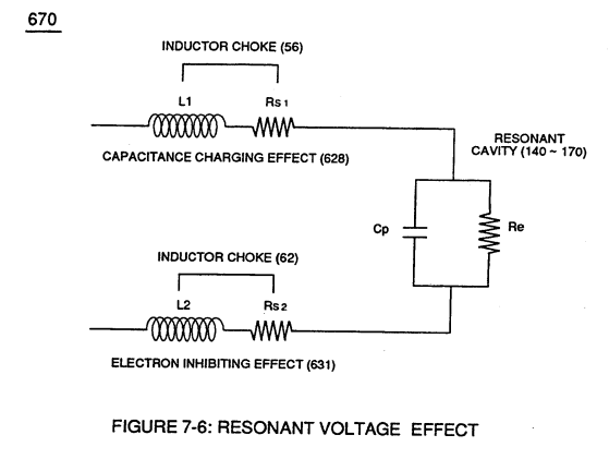
Resonant Voltage Effect (670) of Figure (7-6) · Transformer Action
-
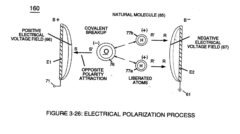
Opposite Electrical Attraction Force (SS' ~ 617 ~ RR' - T3 - SS' ~ 617 - RR') of Figure (7-4) · Electron Bounce Phenomenon
-
(52) of Figure (7-8) · Electron Bounce Phenomenon
-
The figure it sits on · WFC 426 - Illustrations
-
The figure it sits on · WFC 426 - Illustrations
-
The figure it sits on · WFC 426 - Illustrations
-
(720) of Figure (7-11) · 8-2 - Traveling Voltage Wave-Guides
-
The figure it sits on · 8-2 - Traveling Voltage Wave-Guides
-
(690) of Figure (7-8) · 8-2 - Traveling Voltage Wave-Guides
-
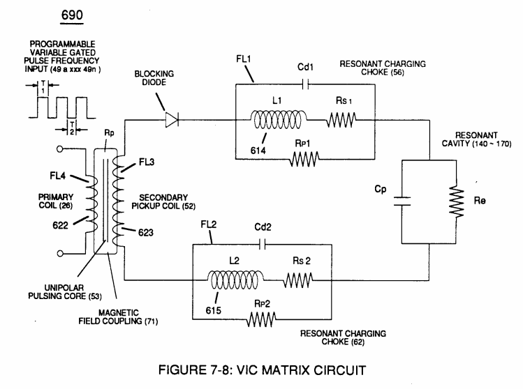
(52) of Figure (7-8) · 8-3 - Electrical Voltage-Pulse Wave-Transmission
-
(650) of Figure (7-4) · 8-4 - State Space (Sp)
-
(690) of Figure (7-8) · 8-6 - VIC Voltage Sync-Pulse Circuit
-
(650) of Figure (7-4) · 8-6 - VIC Voltage Sync-Pulse Circuit
-
(690) of Figure (7-8) · Propagating Electrical Stress
-
Figure (3-34) · Propagating Electrical Stress
-
The figure it sits on · Propagating Electrical Stress
-
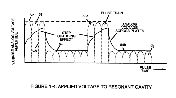
Figure (1-4) · Propagating Electrical Stress
-
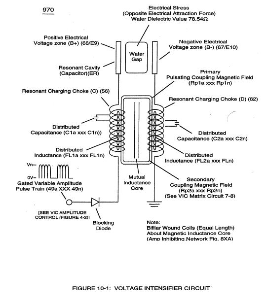
The programmable pulse-frequency (49a xxx 49n) of Figure (10-1) input is simply adjusted to tune-in to the dielectric property of the Water Molecule. · Propagating Electrical Stress
-
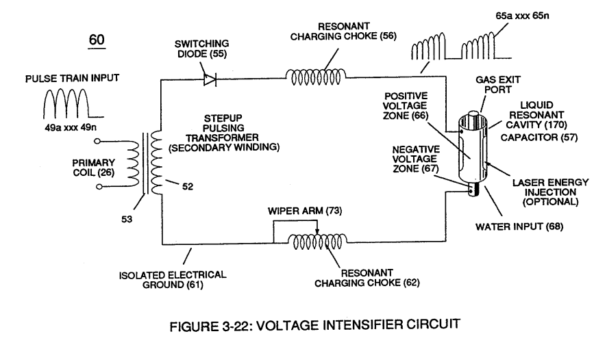
blocking diode (55) of Figure (3-34) · Voltage to Amp Differential Ratio
-
The figure it sits on · WFC 429 - Illustrations
-
(970) of Figure (10-1) · VIC Switchover Circuit
Where it is named · 25
Instant Explosion of Water 1×
-
Capacitor-Gap (Cp)
… ignal distortion" or "signal degradation" (preventing transformer ringing during signal propagation) as elevated voltage levels ( - xx Vc- xx Vd - xx Vn) while allowing the reduction of Capacitor-Gap (Cp) (616) of Figure (7-11) width spacing (57 of Figure 3- 25 ~35 of Figure 6-2) (typically .060 - .010) respectively as illustrated in Tubular Resonant Cavity (170) as to Taper Resonant Cavity (620) of F …
Inductance Reactance (Rs - Cd - FL) 2×
-
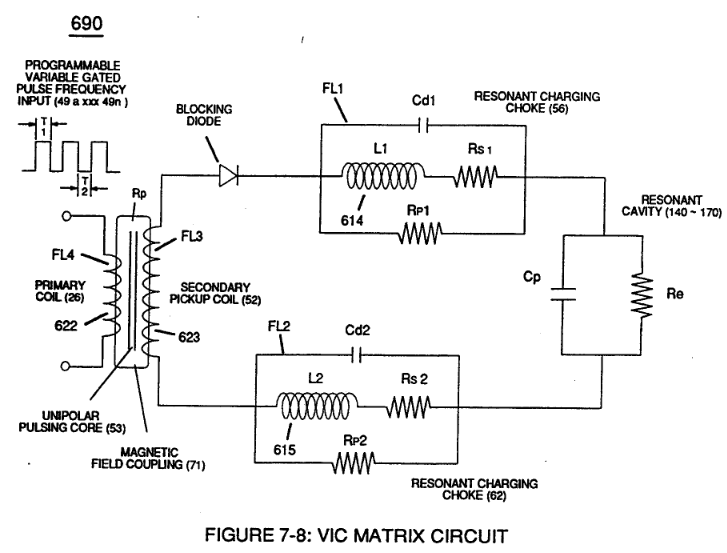
... thereby preventing and inhibiting electron-flow to pass through or arc-over capacitor water-gap (Cp) of Figure (7-8) such electron blocking action is herein called "Electron Inhibiting Effect" (631), as denoted in (670) of Figure (7-6) as to (750) of Figure (7-14).
-
(Cp) of Figure (7-8)
Taper Resonant Capacitor (ERt) 1×
-
Capacitance (Cp)
Capacitance (Cp) of Figure (7-6) as to (690) of Figure (7-8) is determined by the surface area (A) of Electrical Voltage-Plates (E1/E2 - E9/E10), the distance (d) between the Electrical Plates (in inches), and the permittivity (Eo) of the dielectric property of water (85) and, is expressed in the following equation:
Transformer Action 4×
-
Water Gap (Cp)
… e (7-6) to cause "Electron Clustering" (Grouping/collecting negative charged particles at a given point) (700) of Figure (7-9) to produce ''Negative Voltage Potential" ( B- ) at one side of Water Gap (Cp) of Figure (7-8) is accomplished by low electrical power input (Tab 38) when Choke-Coil (62) of Figure (7-1) magnetic field (FL2) (690) of Figure (7-8) during pulse on-time (49) impede "Electron-Flow" …
-
Water Gap (Cp)
Capacitance Charging Effect (628) prevents amp influxing away from Water Gap (Cp) in a similar manner
-
Water Gap (Cp)
... producing "Electrical Stress" (SS' - RR') (B+/B-) across Water Gap (Cp) since both Choke-Coils (56/62) conduct voltage potential (Negative or Positive) during pulsing operations.
-
Water Gap (Cp)
''Negative Voltage Potential" ( B- ) at one side of Water Gap (Cp) of Figure (7-8) & magnetic field (FL2) (690) of Figure (7-8)
8-3 - Electrical Voltage-Pulse Wave-Transmission 1×
-
Water-Gap Capacitor (Cp)
The newly established leading voltage edge (Vpa) and trailing voltage edge (Vpb) being uniform in shape/configuration since both Resonant Charging Chokes (56/Z2 – 62/Z3) resistive values are the same (Typically 11.6 kΩ each) and incoming signal (49a xxx 49n) is electrically linked with Water-Gap Capacitor (Cp) of Figure (7-8) having dielectric liquid of Water (85) there between.
8-4 - State Space (Sp) 2×
-
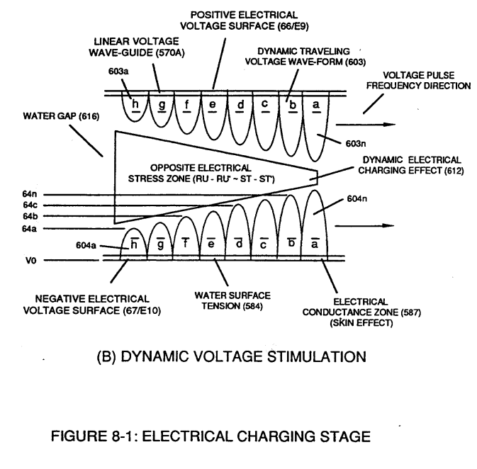
During the electrical-formation (66- Vpa/Vpb - 67- Vpa/Vpb) of each opposite Electrical Voltage-Wave (66-583 - 67-602), opposite electrical attraction force (RR' - SS') of Figure (7-4) is produced across water cap (Cp) of Figure (7-8) which, now, sets up and defines the conditions of “State Space," as illustrated in (770 A/B) of Figure (8-1) as to (650) of Figure (7-4).
-
(Cp) of Figure (7-8)
8-6 - VIC Voltage Sync-Pulse Circuit 2×
-
Water-Gap (Cp)
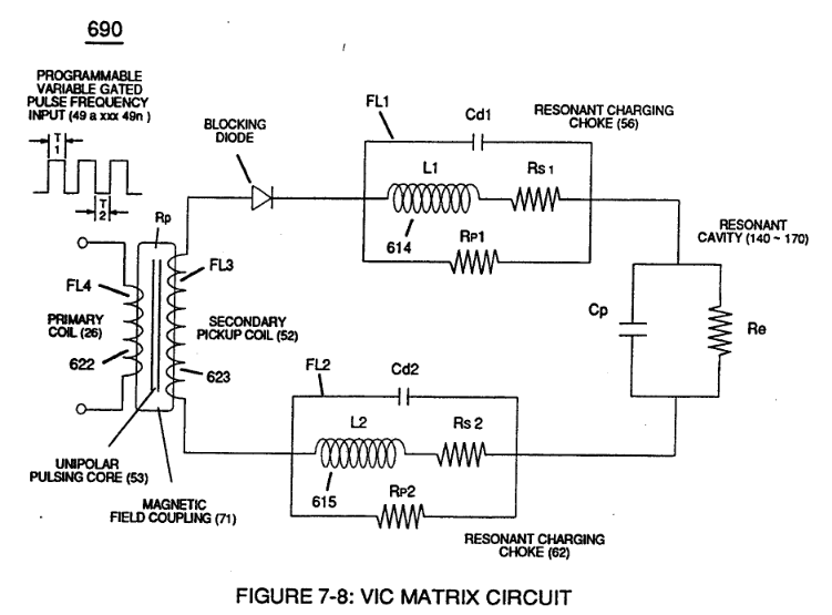
To ensure and maintain Capacitance Charging Effect (650) of Figure (7-4) across Water-Gap (Cp) of (7-8) during applied pulsing operations (49a xxx 49n), Crossover Voltage Wave-Form (780B) as to (780C) of Figure (8-2) is generally utilized by not allowing Convergent Point "Q" of Figure (780B) t …
-
(Cp) of (7-8)
WFC Exhaust Air Reclaimer 1×
-
capacitor gap (Cp)
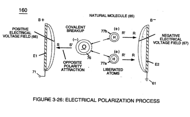
… ectric properties of the airborne gas-molecule to not only activate Covalent Switch-Off phenomenon (550) of Figure (5-8) by restricting amp influxing to cause "Electrical Stress" across capacitor gap (Cp) (690) of Figure (7-6) but, also, elongates the electrically polarized Nitric Oxide NO molecule to change the time share-rate of covalent electron (s)
Propagating Electrical Stress 4×
-
Gap (Cp)
… The length and diameter size of the copper-wire spiral wrapped coil (56/62) of Figure (10-1) being paired together and electrically energized in conjunction with applied Voltage Pulse-Frequency determines how much "Amp Leakage" will occur across capacitor Gap (Cp) while "Voltage Pulse-Potential" (Va xxx Vn/49a xxx 49n) of "Opposite polarity" (B+/B-) is/are allowed to be applied across "Electrical Voltage Plates" (Voltage-Zones) (66/67).
-
Resonant Cavity (Cp)
Pulse-Voltage repetition rate sets up the step-up charging effect Figure (1-3) since the "Resonant Cavity" (Cp) functions as a "Capacitor" (ER) due to the dielectric value of the liquid (or gases) which becomes an integral part of the VIC Circuit, as so illustrated in (650) of Figure (7-4).
-
Resonant Cavity (Cp)
Blocking Diode (52) of Figure (4-9) as to Figure (1-1) allows unipolar pulse-wave to go more positive on each pulse-cycle since the Blocking Diode (52) prevents the Resonant Cavity (Cp) from discharging during pulse off-time, as so illustrated in Figure (1-4) as to (60) of Figure (3-22)
-
Capacitor Gap (Cp)
... allowing the developed "Electrical Stress" (RU/RU' - ST/ST') of Figure (5-1/5-2) across Capacitor Gap (Cp) to go to the farthest point beyond the "State of Equilibrium"
Voltage to Amp Differential Ratio 4×
-
Water Gap (Cp)
The resultant ever increasing pulsating opposite electrical voltage fields (603/604a xxx 603/604n) of Figure (8-1) having superimposed thereon counter opposing Rippling Voltage-Surfaces (64/B+a xxx 64/B-n) [Dynamic Electrical Charging Effect (612) of Figure (8-1B)], now, set ups, causes, and applies ever increasing (rubberbanding effect) Pulsating Opposite Electrical Stress (RU-RU' - ST-ST') across Water Gap (Cp)
-
Resonant Water Gap (Cp)
The greater the Electrical Stress (RU-RU' a xxx ST -ST'n) applied (64B+/64B-a xxx 64B+/64B-), the greater amount of thermal explosive energy (16/gtnta xxx 16/gtntn) of Figure (6-2) as to (70) of Figure (4-5) is released from Resonant Water Gap (Cp) (970) of Figure (10-1), as further illustrated in (70) of Figure (4-5).
-
Water Gap (Cp)
... allowing each/both bifilar coil assembly (56/62a xxx 56/62n -S- SS56/62a xxx SS56/62n) to be electrically and magnetically energized in the same progressive direction toward Water Gap (Cp) and away from blocking diode (55) of Figure (3-34) as to Figure (10-1) and Figure (10-3)
-
Water Gap (Cp)
Stainless Steel bifilarCoil-Stage Assembly (SS56/62a xxx SS56/62n) is electrically placed between Magnet Coil-Stage Assembly (56/62a xxx 56/62n) and Water Gap (Cp) to obtain optimum Voltage to Amp Differential Ratio (Vhighest:Alowest ratio).
Appendix B - Glossary of Applicaiton Notes 3×
-
Water Gap (Cp)
… gure (7-6) to cause "Electron Clustering" (Grouping/collecting negative charged particles at a given point) (700) of Figure (7-9) to produce "Negative Voltage Potential" (B-) at one side of Water Gap (Cp) of Figure (7-8) is accomplished by low electrical power input (Tab 38) when Choke-Coil (62) of Figure (7-1) magnetic field (FL2) (690) of Figure (7-8) during pulse on-time (49) impede "Electron-Flow" since electron mass is composed of electromagnetic matter which interacts with magnetic field strength (FL2). …
-
Water Gap (Cp)
… Capacitance Charging Effect (628) prevents amp influxing away from Water Gap (Cp) in a similar manner ... …
-
Water Gap (Cp)
… producing "Electrical Stress" (SS' - RR') (B+/B-) across Water Gap (Cp) since both Choke-Coils (56/62) conducts voltage potential (Negative or Positive) during pulsing operations.