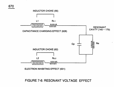
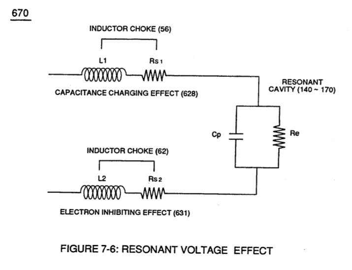
Figure (7-6)
Resonant Voltage Effect
How it is written
- (7-6) 22×
Drawings 7
-
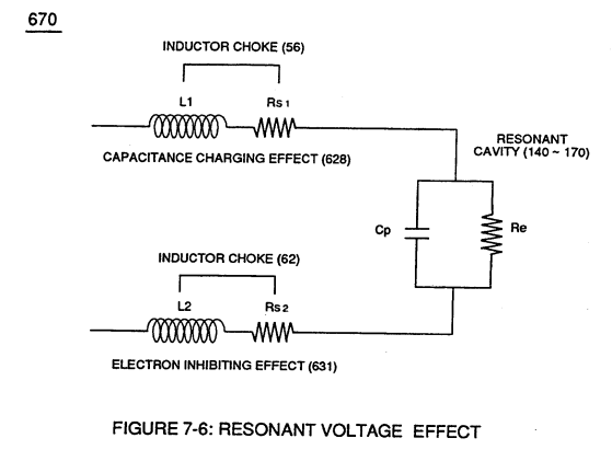
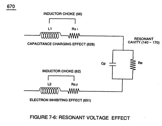
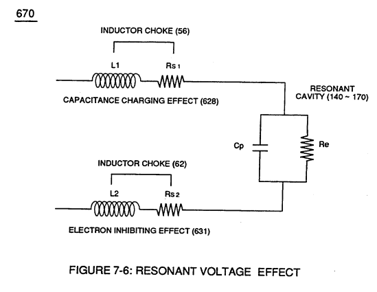
(670) of Figure (7-6) · Inductance (FL)
-
(670) of Figure (7-6) · Capacitance (Cd)
-
(670) of Figure (7-6) · Capacitance (Cd)
-
Captioned as this figure · Taper Resonant Capacitor (ERt)
-
Resonant Capacitor (140 -170) of Figure (7-6) · Capacitance Reactance
-
Resonant Voltage Effect (670) of Figure (7-6) · Transformer Action
-
Captioned as this figure · WFC 426 - Illustrations
On this figure 14
- 85 Water Molecule
- 140 Resonant Capacitor
- 170 Resonant Cavity
- 631 Electron Inhibiting Effect
- 670 Resonant Voltage Effect
- 690 VIC Matrix Circuit
- Cp Water Gap
- ER Excitor-Array
- FL Optimize The Electromagnetic Field Strength
- L1 Inductor
- L2 Inductors
- LC Inductor-Capacitor Circuit
- Re Water
- Rs Series Resistance Value
Where it is named · 22
Inductance (FL) 2×
-
… forms Water-Gap (616) of Figure (7-11) as to Figure (590) of Figure (6-2) having placed there between Dielectric Water Bath (85/Re), as schematically illustrated in matrix outline in (670) of Figure (7-6) as to (690) of Figure (7-8) and further detailed in Electrical Charging Effect (650) of Figure (7-4).
-
(670) of Figure (7-6)
Capacitance (Cd) 5×
-
Inductor (614) and Inductor (615) of Figure (7-1) as to (670) of Figure (7-6) is wound or coil-wrapped (see multi-layer equation Eq. 20) in such a manner as to increase the magnetic flux intensity (D1a xxx D1n) of Figure (7-3) as to (580) as to Figure (6-1) in reference to (710) of Figure (7-10) between the turns (618a xxx 618n) of coil-wrap (640).
-
(670) of Figure (7-6)
-
(670) of Figure (7-6)
Inductance Reactance (Rs - Cd - FL) 6×
-
… eactance not only increases voltage across water-capacitor (ER) beyond applied Voltage Potential (626) of Figure (7-7) but, also, establishes "Impedance Field" (FL) across Inductors (L1-L2) of Figure (7-6) which acts and performs as Resonant Charging Chokes (614/615) of Figure (7-1) once placed on opposite side of capacitor (ER) forming Resonant voltage Effect Circuit (670) of Figure (7-6), as illustra …
-
Inductors (L1-L2) of Figure (7-6)
-
(670) of Figure (7-6)
-
(670) of Figure (7-6)
Taper Resonant Capacitor (ERt) 1×
-
Capacitance (Cp) of Figure (7-6) as to (690) of Figure (7-8) is determined by the surface area (A) of Electrical Voltage-Plates (E1/E2 - E9/E10), the distance (d) between the Electrical Plates (in inches), and the permittivity (Eo) of the dielectric property of water (85) and, is expressed in the following equation:
Capacitance Reactance 2×
-
Resonant Capacitor (140 -170) of Figure (7-6)
Transformer Action 4×
-
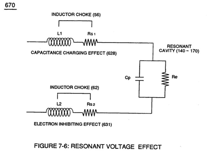
… thereby, allowing Inductance Charging Effect (660) of Figure (7-5) and Resonant Voltage Effect (670) of Figure (7-6) to interact with the dielectric properties of water (Re) to cause and inhibit electron flow (IF) since "electrons" magnetic field (547) of Figure (5-9) locks onto the electromagnetic fields of each e …
-
Resonant Voltage Effect (670) of Figure (7-6)
-
Electron Inhibiting Effect (631) of Figure (7-6)
WFC Exhaust Air Reclaimer 1×
-
… the airborne gas-molecule to not only activate Covalent Switch-Off phenomenon (550) of Figure (5-8) by restricting amp influxing to cause "Electrical Stress" across capacitor gap (Cp) (690) of Figure (7-6) but, also, elongates the electrically polarized Nitric Oxide NO molecule to change the time share-rate of covalent electron (s)