(Re)
Water
Also written Dielectric Coefficient of Water resistance · Dielectric Water Bath
Where it is first named
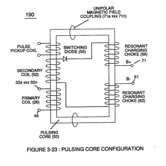
Switching Diode (55) of Figure (3-22) prevents Bidirectional electron flow (current flow in one direction only) since Blocking Diode (55) only conducts "current flow" in the direction of schematic-arrow while being placed in-line with VIC Circuit impedance interaction (R1 + Z2 + Z3 + Re), as mathematically extrapolated in Circuit Equation (Eq 9)
How it is written
- (Re) 10×
- (85/Re) 3× with (85) Water Molecule
- (R1 + Z2 + Z3 + Re) 1× with (R1), (Z2) Resonant Choke Coils Electromagnetic Fields Intensity, (Z3) Resonant Choke Coils Electromagnetic Fields Intensity
- (Rs+Re) 1× with (Rs) Series Resistance Value
Drawings 67
-
Figure 1-1 · RLC CIRCUIT
-
The primary coil is electrically isolated (no electrical connection between primary and secondary coil) to form Voltage Intensifier Circuit (AA) Figure (1-1). · Pulsing Transformer
-
The figure it sits on · Electronic Circuit Design
-
The figure it sits on · Electronic Circuit Design
-
The figure it sits on · Differential Air-Gas Inlet Control
-
The figure it sits on · Differential Air-Gas Inlet Control
-
Water Fuel Injection System (10) of Figure (1) · Water Fuel Injector (Taper Resonant Cavity Chamber)
-
(650) of Figure (7-4) · Amp Inhibiting Circuit Vs Voltage Enhancement
-
Figure (4-9) · Water Fuel Injection System - Page 2
-
...converts water mist (68) into it's component gases hydrogen (77 a/b) oxygen (76) and ambient air gases (97); · Triggering Process
-
Figure (5-6) · Energy Recycling Spectrum
-
(110) of Figure (4-9) · In Application of Usage
-
(57) of Figure (6-2) · In Application of Usage
-
The figure it sits on · Illustrations
-
Activation Process (590) of Figure (6-2) · Voltage Intensifier Coil-Assembly
-
(VIC) coil-assembly (530) of Figure (5-6) · Tri - Coil Construction
-
The figure it sits on · VIC Matrix Circuit
-
Figure (1-1) (Memo WFC 420) · Instant Explosion of Water
-
(628) of Figure (7-7) · Instant Explosion of Water
-
(T2) of Figure (7-8) · Instant Explosion of Water
-
Figure (7-8) · Resistance (Rs)
-
(650) of Figure (7-4) · Resistance (Rs)
-
(110) of Figure (4-9) · Resistance (Rs)
-
(690) of Figure (7-8) · Resistance (Rs)
-
The figure it sits on · Inductance (FL)
-
(670) of Figure (7-6) · Inductance (FL)
-
(690) of Figure (7-8) · Inductance (FL)
-
(650) of Figure (7-4) · Inductance (FL)
-
(532) of Figure (5-6) · Capacitance (Cd)
-
(650) of Figure (7-4) · Capacitance (Cd)
-
(590) of Figure (6-2) · Capacitance (Cd)
-
(670) of Figure (7-6) · Capacitance (Cd)
-
(670) of Figure (7-6) · Capacitance (Cd)
-
(690) of Figure (7-8) · Capacitance (Cd)
-
(690) of Figure (7-8) · Inductance Reactance (Rs - Cd - FL)
-
(627) of Figure (7-7) · Inductance Reactance (Rs - Cd - FL)
-
(547) of Figure (5-9) · Inductance Reactance (Rs - Cd - FL)
-
Figure (7-8) · Inductance Reactance (Rs - Cd - FL)
-
(E1/E2) of Figure (1-1) page (1-13) · Taper Resonant Capacitor (ERt)
-
The figure it sits on · Taper Resonant Capacitor (ERt)
-
(690) of Figure (7-8) · Taper Resonant Capacitor (ERt)
-
Resonant Capacitor (140 -170) of Figure (7-6) · Capacitance Reactance
-
"Voltage Deflection" of Figure (7-4) · Capacitance Reactance
-
690 of Figure 7-8 · Circuit Resistance
-
Resonant Voltage Effect (670) of Figure (7-6) · Transformer Action
-
(547) of Figure (5-9) · Transformer Action
-
Opposite Electrical Attraction Force (SS' ~ 617 ~ RR' - T3 - SS' ~ 617 - RR') of Figure (7-4) · Electron Bounce Phenomenon
-
(52) of Figure (7-8) · Electron Bounce Phenomenon
-
(E9/10) of Figure (6-2) · Voltage Amplitude Switch-Off
-
The figure it sits on · WFC 426 - Illustrations
-
The figure it sits on · WFC 426 - Illustrations
-
The figure it sits on · WFC 426 - Illustrations
-
The figure it sits on · 8-2 - Traveling Voltage Wave-Guides
-
(690) of Figure (7-8) · 8-2 - Traveling Voltage Wave-Guides
-
(52) of Figure (7-8) · 8-3 - Electrical Voltage-Pulse Wave-Transmission
-
(Cp) of Figure (7-8) · 8-4 - State Space (Sp)
-
(650) of Figure (7-4) · 8-4 - State Space (Sp)
-
(690) of Figure (7-8) · 8-6 - VIC Voltage Sync-Pulse Circuit
-
(650) of Figure (7-4) · 8-6 - VIC Voltage Sync-Pulse Circuit
-
(Cp) of (7-8) · 8-6 - VIC Voltage Sync-Pulse Circuit
-
Voltage Intensifier Circuit (110) of Figure (4-9) · WFC Exhaust Air Reclaimer
-
(690) of Figure (7-8) · Propagating Electrical Stress
-
The figure it sits on · Propagating Electrical Stress
-
Blocking Diode (52) of Figure (4-9) · Propagating Electrical Stress
-
Figure (1-1) · Propagating Electrical Stress
-
The figure it sits on · WFC 429 - Illustrations
-
The figure it sits on · The Atom Functioning as an Energy Transporter
Where it is named · 15
Instant Explosion of Water 1×
-
Switching Diode (55) of Figure (3-22) prevents Bidirectional electron flow (current flow in one direction only) since Blocking Diode (55) only conducts "current flow" in the direction of schematic-arrow while being placed in-line with VIC Circuit impedance interaction (R1 + Z2 + Z3 + Re), as mathematically extrapolated in Circuit Equation (Eq 9)
Resistance (Rs) 2×
-
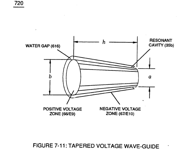
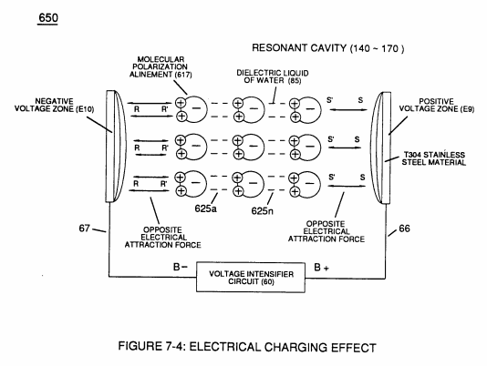
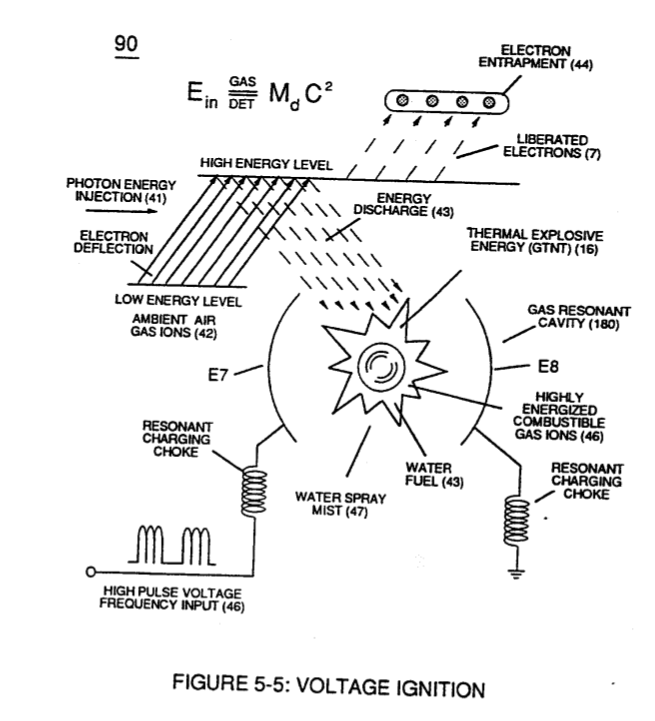
... releasing thermal explosive energy (gtnt) (16) of Figure (4-5) on demand from natural water (85) of Figure (3-26) since the dielectric value (Re) of (Eq.9) of Water Fuel (85) is further approximated in Capacitance Equation (Eq.22), as illustrated in (650) of Figure (7-4) as to Tapered Voltage Wave-Guide (720) of Figure (7-11)
-
Water (Re)
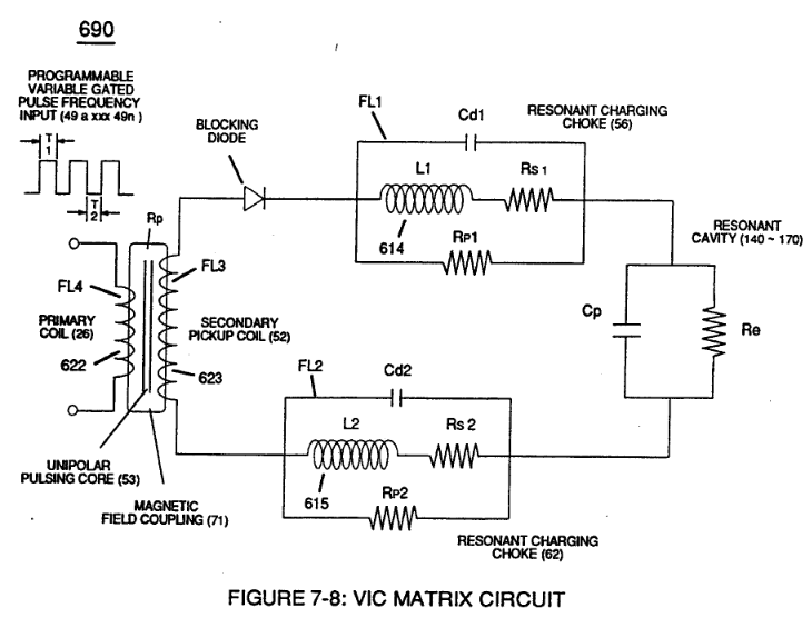
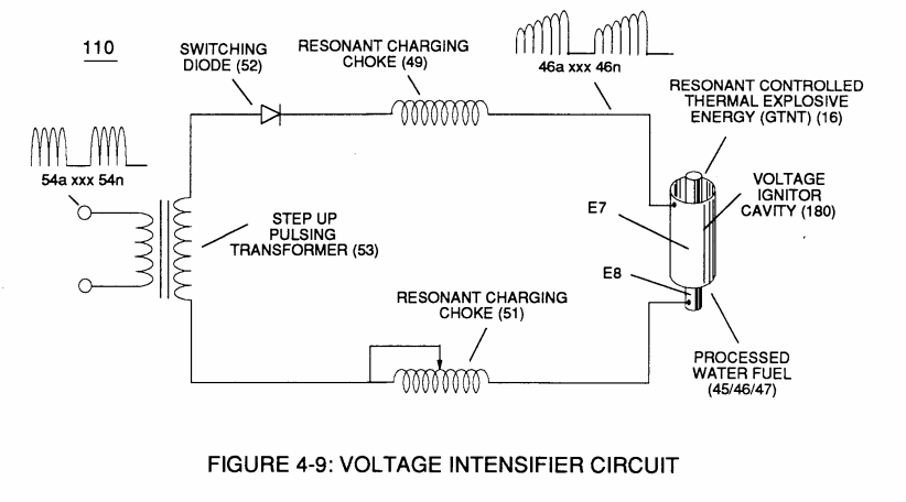
... allowing the dielectric value of Water (Re) to be a part of Voltage Intensifier Circuit (110) of Figure (4-9) capability of restricting amp flow during Voltage Pulsing Operation (49a xxx 49n) of (620) of Figure (7-1) as to VIC Matrix Circuit (690) of Figure (7-8)
Inductance (FL) 2×
-
Dielectric Water Bath (85/Re)
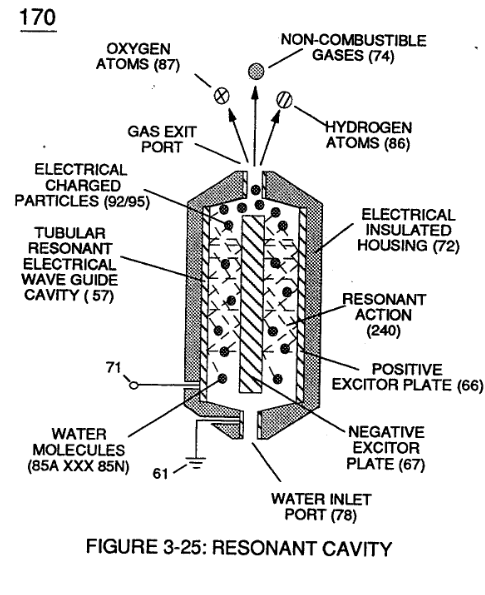
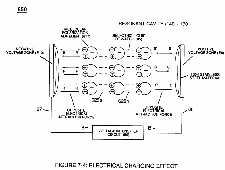
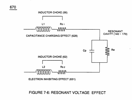
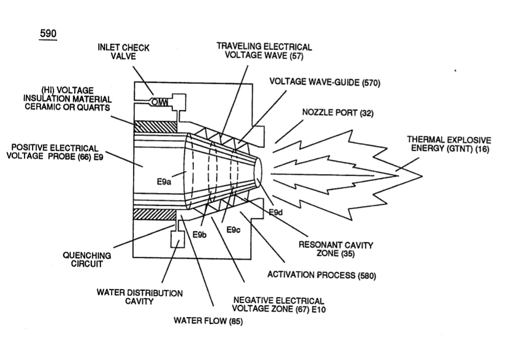
… 1) is formed when outer tapered surface (66) and inner tapered surface (67) forms Water-Gap (616) of Figure (7-11) as to Figure (590) of Figure (6-2) having placed there between Dielectric Water Bath (85/Re), as schematically illustrated in matrix outline in (670) of Figure (7-6) as to (690) of Figure (7-8) and further detailed in Electrical Charging Effect (650) of Figure (7-4).
-
... interacting Distributed Capacitance (Cda xxx Cdn) and Distributed Inductance (D1a xxx D1n) of Figure (7-3) of Inductor Coil (614) of (7-1) with "Electrical Charging Effect" brought on by the dielectric value of water bath (85/Re), as pictorially illustrated in (650) of Figure (7-4).
Capacitance (Cd) 1×
-
Capacitor (E9/E10) of Figure (7-1) as to Figure (650) of Figure (7-4) in direct relationship to Water Gap (616) becomes Taper Resonant Cavity (720) of Figure (7-11) as shown in (590) of Figure (6-2) since Water Gap (616) is occupied by a dielectric liquid (Re) as herein before identified as natural water (85) having no electrolyte added thereto
Inductance Reactance (Rs - Cd - FL) 1×
-
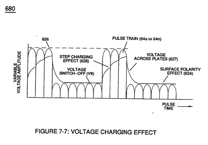
… urage and promote "Electron Bounce" phenomenon (700) of Figure (7-9) while adjusting (programmable pulse wave-form) input signal Pulse-Frequency (49a xx 49n) to "tune-in" to the "dielectric property" (Re) of water (85) causing amp flow to be reduce to a minimum value while allowing voltage potential (627) of Figure (7-7) to go toward infinity if the electronic components would allow it to happen, as g …
Taper Resonant Capacitor (ERt) 1×
-
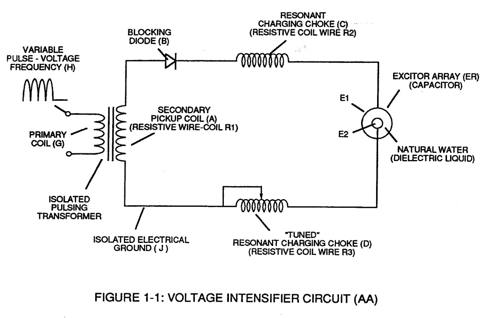
Capacitor (ER) is automatically formed when dielectric liquid of water (Re) is placed between Electrical Conducting Plates (E1/E2) of Figure (1-1) page (1-13) (Memo WFC 420).
Capacitance Reactance 1×
-
Capacitance Reactance is determined by the insulation resistance (Rs+Re) and Inductance (L1/L2) interacting together during D.C. Pulsing.
Circuit Resistance 1×
-
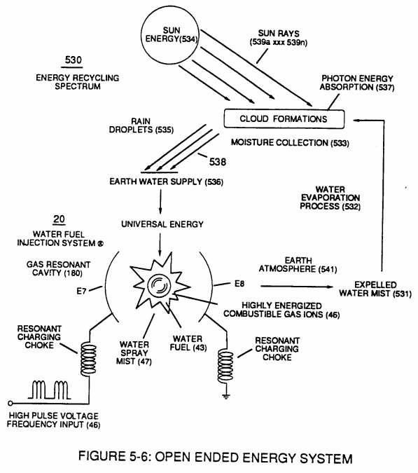
... each choke-coil (LIIL2) being of the same impedance value since both coil-wraps (56/62) are Bifilar wound together onto a single spool-bobbin, (Re) is the dielectric property of water and it's resistive value is typically (78.54 Q) since "rain water" (85f) contains less than 20ppm of any type of contaminates due to Water Evaporation Process (530) of Figure (5-6).
Transformer Action 1×
-
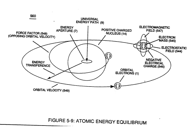
… thereby, allowing Inductance Charging Effect (660) of Figure (7-5) and Resonant Voltage Effect (670) of Figure (7-6) to interact with the dielectric properties of water (Re) to cause and inhibit electron flow (IF) since "electrons" magnetic field (547) of Figure (5-9) locks onto the electromagnetic fields of each energized choke coils (FL1/FL2) during Voltage Excitation …
Electron Bounce Phenomenon 2×
-
Water (Re)
… 2 - 56 - 62) simultaneously during each and every pulse on-time (T1a xxx T1n) as programmable pulse-train (49a xxx 49n T3 - 49a xxx 49n) is adjusted to "Tune - in" to the dielectric property of Water (Re)
-
Dielectric Coefficient of Water resistance (Re)
… henomenon (EbP), Voltage Coefficient of Inductance (F11/F12), Voltage Coefficient of Capacitance (Cd1/Cd2), Voltage Coefficient of Resistance (Rs1/Rs2), and Dielectric Coefficient of Water resistance (Re) allows Voltage Potential (Vo - Vn) of opposite electrical polarity to perform work (SS' _ 617 _ RR') without amp influxing, thus, not allowing the introduction of electron flow into Hydrogen Fracturi …
8-2 - Traveling Voltage Wave-Guides 2×
-
The surface tension of water (584) adjacent to both voltage surfaces (E9 / EI0) further aids the transmission of voltage potential (66/67) since Electrical Charging Effect (585) of Figure (7-4) does not change or alter the dielectric value of water (Re).
-
Voltage Intensifier Matrix Circuit (690) of Figure (7-8) electrically connected with resistive liquid (85/Re) (forming Resonant Water Gap "Cp" of Figure 7-8) propagates the transmission of Traveling Voltage Wave-Form (57) of Figure (6-2) as to (770) of Figure(8-1) by the functional relationship of Circuit Resistance Equation (Eq 9) during programmable Voltage Pulsing operations (49a xxx 1'3 xxx 49n) of Figure (8-2).