(E10)
Capacitor
Also written Voltage Zones · negative electrical voltage surface · electrical conducting plates · Electrical Voltage-Plates
Where it is first named
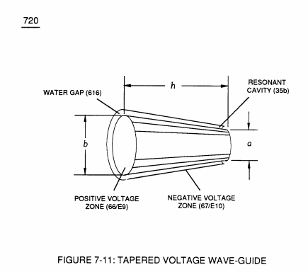
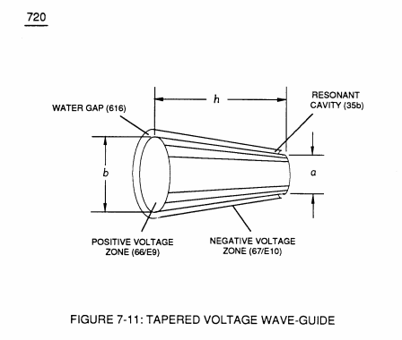
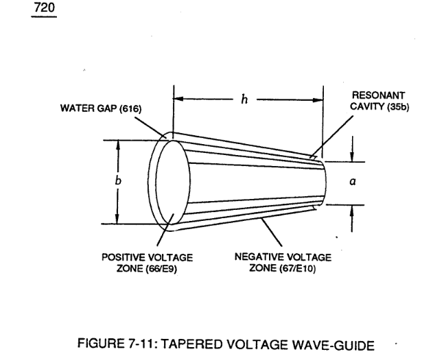
Capacitor (E9/E10) of figure (6-2) as to (720) of Figure (7-11) is formed when outer tapered surface (66) and inner tapered surface (67) forms Water-Gap (616) of Figure (7-11) as to Figure (590) of Figure (6-2) having …
How it is written
- (E9/E10) 11× with (E9) Capacitor
- (66/E9 – 67/E10) 1× with (66) Positive Voltage Potential, (E9) Capacitor, (67) Opposite Polarity
- (67/E10) 1× with (67) Opposite Polarity
- (E1/E2 - E9/E10) 1× with (E1) Voltage Zones, (E2) Voltage Zones, (E9) Capacitor
Drawings 88
-
(650) of Figure (7-4) · Amp Inhibiting Circuit Vs Voltage Enhancement
-
(616) of Figure (7-11) · Instant Explosion of Water
-
(650) of Figure (7-4) · Resistance (Rs)
-
(720) of Figure (7-11) · Inductance (FL)
-
(720, 616) of Figure (7-11) · Inductance (FL)
-
Carries this number · Inductance (FL)
-
Capacitor (E9/E10) of Figure (7-11) · Inductance (FL)
-
(650) of Figure (7-4) · Inductance (FL)
-
(720) of Figure (7-11) · Capacitance (Cd)
-
(650) of Figure (7-4) · Capacitance (Cd)
-
(730) of Figure (7-12) · Taper Resonant Capacitor (ERt)
-
diagram 720 of Figure 7-11 · Taper Resonant Capacitor (ERt)
-
"Voltage Deflection" of Figure (7-4) · Capacitance Reactance
-
Opposite Electrical Attraction Force (SS' ~ 617 ~ RR' - T3 - SS' ~ 617 - RR') of Figure (7-4) · Electron Bounce Phenomenon
-
Traveling Electrical Voltage Wave-forms (730a - b - c) of Figure (7-12) · Electron Bounce Phenomenon
-
Compressional Wave-form (B) of Figure (7-12) · Voltage Amplitude Switch-Off
-
Carries this number · Mode of Operability
-
Carries this number · WFC 426 - Illustrations
-
Carries this number · WFC 426 - Illustrations
-
(720) of Figure (7-11) · 8-2 - Traveling Voltage Wave-Guides
-
Carries this number · 8-2 - Traveling Voltage Wave-Guides
-
(650) of Figure (7-4) · 8-4 - State Space (Sp)
-
(770 B) of Figure (8-1) · 8-4 - State Space (Sp)
-
(585) of Figure (8-1) · 8-4 - State Space (Sp)
-
(770A) of Figure (8-1) · 8-5 - Energy Vectoring (Ev)
-
(650) of Figure (7-4) · 8-6 - VIC Voltage Sync-Pulse Circuit
-
Carries this number · WFC 427 Illustrations
-
"Voltage Tickling of State Space" (770A) of Figure (8-1) · WFC Exhaust Air Reclaimer
-
"Voltage Tickling of State Space" (770B) of Figure (8-1) · WFC Exhaust Air Reclaimer
-
Carries this number · Propagating Electrical Stress
-
The programmable pulse-frequency (49a xxx 49n) of Figure (10-1) input is simply adjusted to tune-in to the dielectric property of the Water Molecule. · Propagating Electrical Stress
-
Carries this number · Quartz Tube Configuration & Operational Parameters
-
Carries this number · Quartz Tube Configuration & Operational Parameters
-
... establishing variable Dynamic Electrical Charging Effect (612). · Quartz Tube Configuration & Operational Parameters
-
Carries this number · WFC 429 - Illustrations
-
Carries this number · Wobbling Effect
-
(970) of Figure (10-1) · VIC Switchover Circuit
-
(57) of Figure (6-2) · In Application of Usage
-
Activation Process (590) of Figure (6-2) · Voltage Intensifier Coil-Assembly
-
"Voltage Intensity of Opposite Potential" (600) of Figure (6-3) · Voltage Intensifier Coil-Assembly
-
The figure it sits on · WFC 425 - Illustrations
-
The figure it sits on · VIC Matrix Circuit
-
Voltage Intensifier Circuit (620) of Figure (7-1) · Instant Explosion of Water
-
(T2) of Figure (7-8) · Instant Explosion of Water
-
(620) of Figure (7-1) · Instant Explosion of Water
-
Figure (7-8) · Resistance (Rs)
-
(620) of Figure (7-1) · Resistance (Rs)
-
(690) of Figure (7-8) · Resistance (Rs)
-
(600) of Figure (6-3) · Inductance (FL)
-
(614) of Figure (7-1) · Inductance (FL)
-
(690) of Figure (7-8) · Inductance (FL)
-
Inductor (614) of Figure (7-1) · Inductance (FL)
-
(600) of Figure (6-3) · Inductance (FL)
-
(614) of (7-1) · Inductance (FL)
-
Figure (7-1) · Capacitance (Cd)
-
(590) of Figure (6-2) · Capacitance (Cd)
-
(690) of Figure (7-8) · Capacitance (Cd)
-
(690) of Figure (7-8) · Inductance Reactance (Rs - Cd - FL)
-
Figure (7-8) · Inductance Reactance (Rs - Cd - FL)
-
(620) of Figure (7-1) · Inductance Reactance (Rs - Cd - FL)
-
(690) of Figure (7-8) · Taper Resonant Capacitor (ERt)
-
(see diagram 720 of Figure 7-11) · Taper Resonant Capacitor (ERt)
-
690 of Figure 7-8 · Circuit Resistance
-
Choke-Coil (62) of Figure (7-1) · Transformer Action
-
(52) of Figure (7-8) · Electron Bounce Phenomenon
-
(E9/10) of Figure (6-2) · Voltage Amplitude Switch-Off
-
The figure it sits on · WFC 426 - Illustrations
-
The figure it sits on · 8-1 - Propagating "Resonant Action" By Voltage Tickling of State Space
-
(730A) of Figure (7-12) · 8-2 - Traveling Voltage Wave-Guides
-
(570) of Figure (7-12) · 8-2 - Traveling Voltage Wave-Guides
-
(690) of Figure (7-8) · 8-2 - Traveling Voltage Wave-Guides
-
(770) of Figure(8-1) · 8-2 - Traveling Voltage Wave-Guides
-
(770) of Figure (8-1) · 8-3 - Electrical Voltage-Pulse Wave-Transmission
-
(52) of Figure (7-8) · 8-3 - Electrical Voltage-Pulse Wave-Transmission
-
(Cp) of Figure (7-8) · 8-4 - State Space (Sp)
-
(770 A) of Figure (8-1) · 8-4 - State Space (Sp)
-
(730) of Figure (7-12) · 8-5 - Energy Vectoring (Ev)
-
(612) of Figure (8-1) · 8-5 - Energy Vectoring (Ev)
-
(620) of Figure (7-1) · 8-6 - VIC Voltage Sync-Pulse Circuit
-
(690) of Figure (7-8) · 8-6 - VIC Voltage Sync-Pulse Circuit
-
(Cp) of (7-8) · 8-6 - VIC Voltage Sync-Pulse Circuit
-
(730C) of Figure (7-12) · 8-7 - Application of Usage
-
(730A) of Figure (7-12) · 8-7 - Application of Usage
-
(690) of Figure (7-8) · Propagating Electrical Stress
-
"Resonant Charging Choke" (56) of Figure (7-1) · Propagating Electrical Stress
-
Dynamic Electrical Charging Effect (612) of Figure (8-1) · Propagating Electrical Stress
-
(620) of figure (7-1) · Voltage to Amp Differential Ratio
-
The figure it sits on · WFC 429 - Illustrations
Where it is named · 14
Inductance (FL) 4×
-
Capacitor (E9/E10)
Capacitor (E9/E10) of figure (6-2) as to (720) of Figure (7-11) is formed when outer tapered surface (66) and inner tapered surface (67) forms Water-Gap (616) of Figure (7-11) as to Figure (590) of Figure (6-2) having …
-
Capacitor (E9/E10)
Component Reactance to D.C. pulsing transforms Inductor (614) of Figure (7-1) / Capacitor (E9/E10) of Figure (7-11) LC circuit of Figure (7-2) into an Resonant Charging Choke (614) which steps up an unipolar oscillation of an given charging frequency with the effective capacitance of a pulse-formi …
-
Voltage Zones (E9/E10)
… nipolar oscillation of an given charging frequency with the effective capacitance of a pulse-forming network (64a xxx 64n) of Figure (7-1) as to (600) of Figure (6-3) in order to charge Voltage Zones (E9/E10) to a higher potential beyond applied voltage input
Capacitance (Cd) 3×
-
Capacitor (E9/E10)
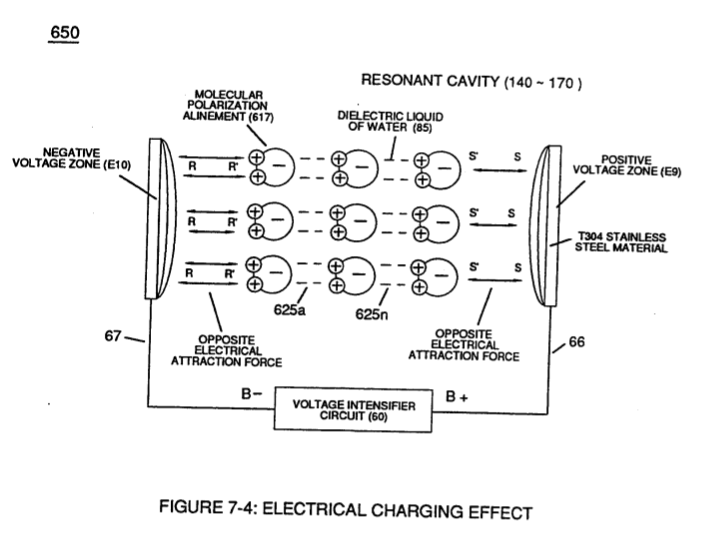
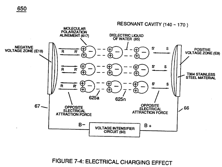
Capacitor (E9/E10) of Figure (7-1) as to Figure (650) of Figure (7-4) in direct relationship to Water Gap (616) becomes Taper Resonant Cavity (720) of Figure (7-11) as shown in (590) of Figure (6-2) since Water Gap (616) is occupied by a dielectric liquid (Re) as herein before identified as natural water (85) having no electrolyte added thereto
-
In like manner, the stainless steel (s/s) T304 material that forms Voltage Zones (E9/EI0) undergo particle alignment of its atomic structure within the atomic infrastructure of plate-material (E9/E10) when exposed to the same applied electrical voltage fields (66/67) after a pre-set time
-
electrical conducting plates (E9/E10)
… nant Cavity (720) of Figure (7-11) as to (650) of Figure (7-4) forms capacitor (ER) of Figure (7-1) when the dielectric liquid of water (85) is placed or injected between electrical conducting plates (E9/E10) while applied voltage Potential of opposite polarity (66/67) is directly exposed to Water Molecules (85a xxx 85n), as depicted in Taper Resonant Cavity (590) of Figure (6-2) as to (650) of Figure (7- …
Taper Resonant Capacitor (ERt) 2×
-
The dielectric property of water (being 78.54 ohms @ 25° C) permits the storage of '"Electrical Charge" when a potential voltage difference exists between Electrical Voltage-Plates (E1/E2) as to (E9/E10).
-
Electrical Voltage-Plates (E1/E2 - E9/E10)
Capacitance (Cp) of Figure (7-6) as to (690) of Figure (7-8) is determined by the surface area (A) of Electrical Voltage-Plates (E1/E2 - E9/E10), the distance (d) between the Electrical Plates (in inches), and the permittivity (Eo) of the dielectric property of water (85) and, is expressed in the following equation:
8-2 - Traveling Voltage Wave-Guides 4×
-
negative electrical voltage surface (67/E10)
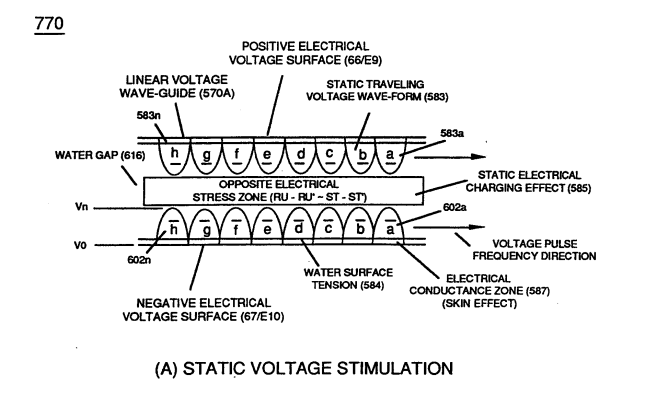
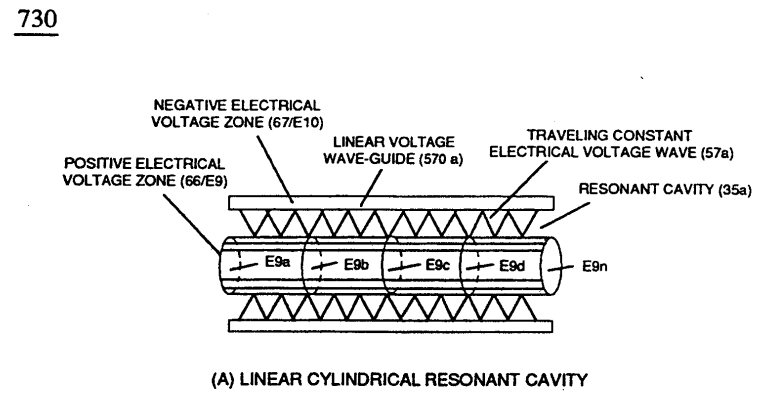
… ing Voltage Wave-guide (570a) of Figure (7-12) (WFC Memo 426) as to (770) of Figure (8-1) is physically formed when positive electrical voltage surface (66/E9) and negative electrical voltage surface (67/E10) are placed in parallel space relationship to form voltage surfaces (E9/E10) about an cylindrical axis of rotation having space-gap (35) there between and thus, fanning Cylindrical Resonant Cavity (73 …
-
… Figure (8-1) is physically formed when positive electrical voltage surface (66/E9) and negative electrical voltage surface (67/E10) are placed in parallel space relationship to form voltage surfaces (E9/E10) about an cylindrical axis of rotation having space-gap (35) there between and thus, fanning Cylindrical Resonant Cavity (730A) of Figure (7-12) as to (770A) of Figure (8-1) when space-gap (616) of Fi …
-
Together, the Voltage Coefficient of Water (e/Eo) of Equation (Eq 21) and the Voltage Coefficient of the stainless steel (s/s) material fanning voltage surfaces (E9/E10), now, allows the establishment and performance of Traveling Electrical Voltage Wave-Guide (583/602) since electrical conductance zone (587) between electrical surface (S) (E9/E10) and the dielectric …
-
… ng voltage surfaces (E9/E10), now, allows the establishment and performance of Traveling Electrical Voltage Wave-Guide (583/602) since electrical conductance zone (587) between electrical surface (S) (E9/E10) and the dielectric surface tension of water (584) acts and performs as a electrical conductor (Skin Effect)
Quartz Tube Configuration & Operational Parameters 1×
-
Voltage Zones (66/E9 – 67/E10)
The Electrical Conduction Zone (587) (Skin Effect) between the dielectric gas medium (919) and the Electrical Contact Surface of the inside surface area of the Voltage Wave-Guides (66/67) allows Unipolar Pulse Train (583a/602a-583b/602b - 583n/602n) to travel the entire length of the Voltage Wave Guides that make up Voltage Zones (66/E9 – 67/E10).