(Cd) · also written as a run, Cda xxx Cdn
Distributed Capacitance
Where it is first named
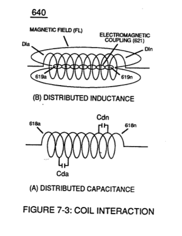
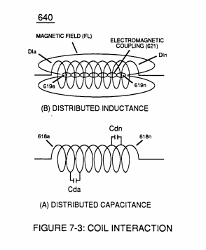
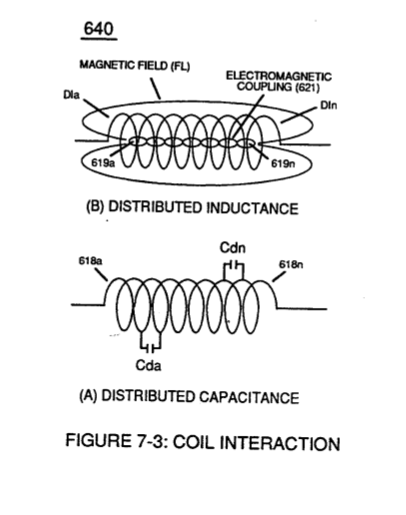
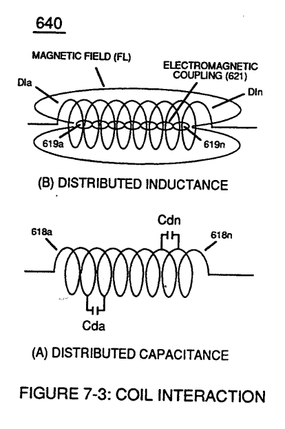
... interacting Distributed Capacitance (Cda xxx Cdn) and Distributed Inductance (D1a xxx D1n) of Figure (7-3) of Inductor Coil (614) of (7-1) with "Electrical Charging Effect" brought on by the dielectric value of water bath (85/Re), as pictorially illustrated in (650) of Figure (7-4).
How it is written
- (Cda xxx Cdn) 6×
- (Cd) 1×
- (Cda xxx Coo) 1× with (Coo)
Cda xxx Cdn is Meyer's shorthand for a run of the same thing: Cda is the first, Cdn the last, and the x's stand for however many lie between. Every stage of the run is this one numeral. A pair before the letters, 583/602a, is a run of two things that go together, one of each per stage.
Drawings 26
-
Distributed Capacitance (Cda xxx Cdn) of Figure (7-3) · Electron Bounce Phenomenon
-
Distributed Capacitance (Cda xxx Cdn) of Figure (7-3) · Electron Bounce Phenomenon
-
The figure it sits on · VIC Matrix Circuit
-
(T2) of Figure (7-8) · Instant Explosion of Water
-
(FI) of Figure (7-3b) · Instant Explosion of Water
-
Figure (7-8) · Resistance (Rs)
-
(690) of Figure (7-8) · Resistance (Rs)
-
(690) of Figure (7-8) · Inductance (FL)
-
Figure (7-3) · Inductance (FL)
-
(690) of Figure (7-8) · Capacitance (Cd)
-
(690) of Figure (7-8) · Inductance Reactance (Rs - Cd - FL)
-
Figure (7-8) · Inductance Reactance (Rs - Cd - FL)
-
Figure (7-3) · Multi-layer Coil
-
(690) of Figure (7-8) · Taper Resonant Capacitor (ERt)
-
690 of Figure 7-8 · Circuit Resistance
-
(52) of Figure (7-8) · Electron Bounce Phenomenon
-
The figure it sits on · WFC 426 - Illustrations
-
(690) of Figure (7-8) · 8-2 - Traveling Voltage Wave-Guides
-
(52) of Figure (7-8) · 8-3 - Electrical Voltage-Pulse Wave-Transmission
-
(Cp) of Figure (7-8) · 8-4 - State Space (Sp)
-
(690) of Figure (7-8) · 8-6 - VIC Voltage Sync-Pulse Circuit
-
(Cp) of (7-8) · 8-6 - VIC Voltage Sync-Pulse Circuit
-
(690) of Figure (7-8) · Propagating Electrical Stress
-
"bifilar" wrapped coils (Figure 7-3) · Propagating Electrical Stress
-
The figure it sits on · WFC 429 - Illustrations
-
The figure it sits on · VIC Switchover Circuit
Where it is named · 8
Inductance (FL) 1×
-
Distributed Capacitance (Cda xxx Cdn)
... interacting Distributed Capacitance (Cda xxx Cdn) and Distributed Inductance (D1a xxx D1n) of Figure (7-3) of Inductor Coil (614) of (7-1) with "Electrical Charging Effect" brought on by the dielectric value of water bath (85/Re), as pictorially illustrated in (650) of Figure (7-4).
Capacitance (Cd) 1×
-
The circular-spiral turns of wire (forming parallel electrical surfaces) is separated by an Insulated Dielectric Coating Material which forms a series of capacitors (Cda xxx Cdn) when magnetic flux-lines (619a xxx 619n) produce Electromagnetic Coupling Field (621) during pulse on-time (T1), as illustrated in (640) of Figure (7-3) as to (690) of Figure (7-8).
Inductance Reactance (Rs - Cd - FL) 1×
-
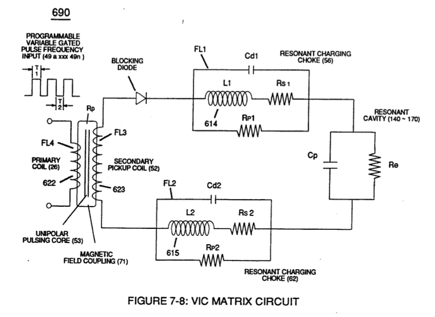
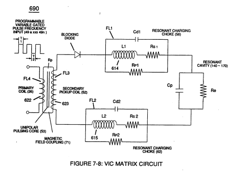
Inductance Reactance occurs when resistance (Rs), capacitance (Cd), and Inductance (FL) interacts together during D.C. Pulsing (49a xxx 49n), as schematically depicted in (690) of Figure (7-8).
Multi-layer Coil 1×
-
Inductance of a multi-layer coil of rectangular cross section can be computed by below formula when optimizing maximum distributed capacitance (Cda xxx Coo) and distributed inductance (Dla xxx Dln) of Figure (7-3) to intensify Inductance Field Strength (FLa xxx FLn) to function as a voltage multiplier in switch-off conditions (612a xxx 612n), as illustrated in (710) of ~ . …
Electron Bounce Phenomenon 2×
-
Distributed Capacitance (Cda xxx Cdn)
.... causing mutual inductance (μ1) (see equations Eq 28 thru Eq 30) to transform Distributed Capacitance (Cda xxx Cdn) of Figure (7-3) of each inductance coils (52 - 56 - 62) into a coherent Voltage Potential (Yo •..• Vn) equaling the sum of Voltage Potential (Vp) developed across each Pickup Coils (VpT + Vp1 + Vp2)
-
Distributed Capacitance (Cda xxx Cdn)
Distributed Capacitance (Cda xxx Cdn) of Figure (7-3)
Voltage to Amp Differential Ratio 1×
-
… gnet bifilar-coil (56/62) is placed on top of Stainless Steel bifilar-coil (SS56/62) to maximize mutual inductance coil-field (Rp2) (adding Rp1+Rp2) of (690) of Figure (7-8) to cause coil capacitance (Cda xxx Cdn) to help maintain and even increase pulse voltage amplitude (xxx Vn + Vn 1 + Vn2 + Vn .... …
VIC Switchover Circuit 1×
-
distributed capacitance (Cda xxx Cdn)
While, the distributed capacitance (Cda xxx Cdn) of each coil experiencing inductance coupling (619) elevates applied voltage level (Vn) to a higher voltage amplitude (increasing voltage intensity) required to deflect the bipolar water molecule to a given or pre-selected distance.