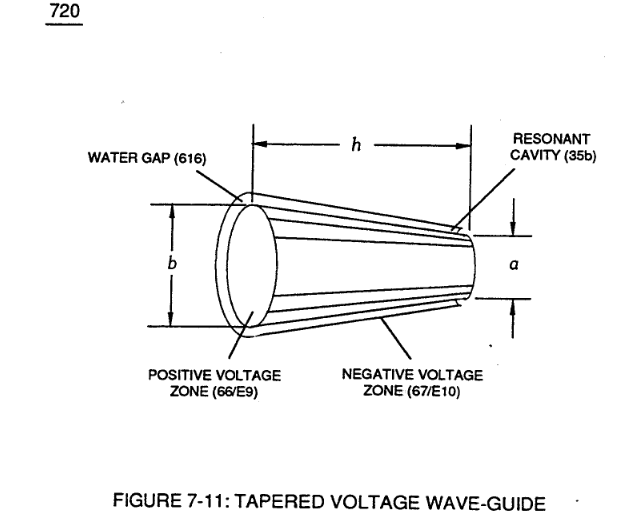
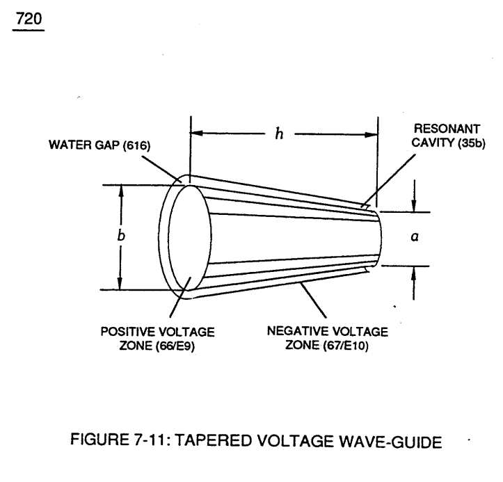
Figure (7-11)
Tapered Voltage Wave-guide
How it is written
- (7-11) 20×
Drawings 9
-
(616) of Figure (7-11) · Instant Explosion of Water
-
(720) of Figure (7-11) · Inductance (FL)
-
(720, 616) of Figure (7-11) · Inductance (FL)
-
Capacitor (E9/E10) of Figure (7-11) · Inductance (FL)
-
(720) of Figure (7-11) · Capacitance (Cd)
-
(see diagram 720 of Figure 7-11) · Taper Resonant Capacitor (ERt)
-
diagram 720 of Figure 7-11 · Taper Resonant Capacitor (ERt)
-
Captioned as this figure · WFC 426 - Illustrations
-
(720) of Figure (7-11) · 8-2 - Traveling Voltage Wave-Guides
On this figure 8
- 66 Positive Voltage Potential
- 67 Opposite Polarity
- 616 Water Gap
- 720 Taper Resonant Cavity
- Cp Water Gap
- E9 Capacitor
- E10 Capacitor
- V Voltage Amplitude
Where it is named · 20
Instant Explosion of Water 2×
-
… "signal degradation" (preventing transformer ringing during signal propagation) as elevated voltage levels ( - xx Vc- xx Vd - xx Vn) while allowing the reduction of Capacitor-Gap (Cp) (616) of Figure (7-11) width spacing (57 of Figure 3- 25 ~35 of Figure 6-2) (typically .060 - .010) respectively as illustrated in Tubular Resonant Cavity (170) as to Taper Resonant Cavity (620) of Figure (7-1).
-
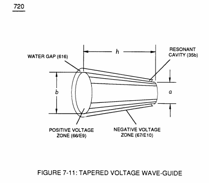
(616) of Figure (7-11)
Resistance (Rs) 3×
-
(66/67) of Figure (7-11)
-
... releasing thermal explosive energy (gtnt) (16) of Figure (4-5) on demand from natural water (85) of Figure (3-26) since the dielectric value (Re) of (Eq.9) of Water Fuel (85) is further approximated in Capacitance Equation (Eq.22), as illustrated in (650) of Figure (7-4) as to Tapered Voltage Wave-Guide (720) of Figure (7-11)
Inductance (FL) 7×
-
(720) of Figure (7-11)
-
Capacitor (E9/E10) of figure (6-2) as to (720) of Figure (7-11) is formed when outer tapered surface (66) and inner tapered surface (67) forms Water-Gap (616) of Figure (7-11) as to Figure (590) of Figure (6-2) having placed there between Dielectric Water Bath (85/Re), as schematically illustrated in matrix outline in (670) of Figure (7-6) as to (690) of Figure (7-8) and f …
-
(720, 616) of Figure (7-11)
-
Component Reactance to D.C. pulsing transforms Inductor (614) of Figure (7-1) / Capacitor (E9/E10) of Figure (7-11) LC circuit of Figure (7-2) into an Resonant Charging Choke (614) which steps up an unipolar oscillation of an given charging frequency with the effective capacitance of a pulse-forming network (64a x …
-
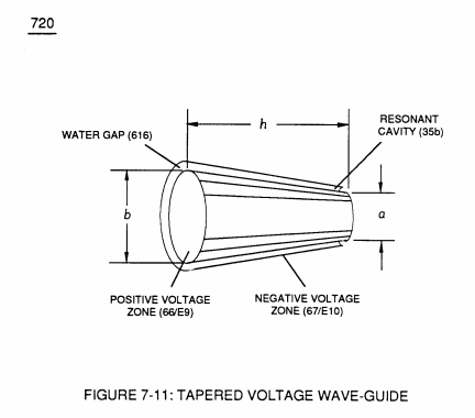
Capacitor (E9/E10) of Figure (7-11)
Capacitance (Cd) 4×
-
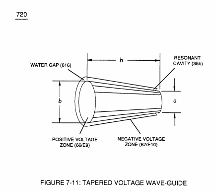
Capacitor (E9/E10) of Figure (7-1) as to Figure (650) of Figure (7-4) in direct relationship to Water Gap (616) becomes Taper Resonant Cavity (720) of Figure (7-11) as shown in (590) of Figure (6-2) since Water Gap (616) is occupied by a dielectric liquid (Re) as herein before identified as natural water (85) having no electrolyte added thereto
-
(720) of Figure (7-11)
-
(720) of Figure (7-11)
Taper Resonant Capacitor (ERt) 2×
-
(see diagram 720 of Figure 7-11)
-
diagram 720 of Figure 7-11
8-2 - Traveling Voltage Wave-Guides 2×
-
(720) of Figure (7-11)