(FL2) · also written as a run, FL2a xxx FL2n
Distributed Inductance
Also written Inductance Fields · Choke Coils · Coefficient of Inductance · inductance field strength · Inductance Field · Inductor Field
Where it is first named
… piral-wrapped coils being paired together, also, causes voltage level enhancement beyond applied voltage input since the "Distributed Capacitance" (Cl xxx Cln =C2a xxx C2n) / "Distributed Inductance" (FL1a xxx FL1n = FL2a xxx FL2n) of said "Bifilar" wrapped coils encourages the compounding effect (increasing magnetic field-strength during each pulsing cycle) of electromagnetic field-strength (Rpla xxx Rpin = Rp2a xxx Rp2n) (mut …
How it is written
- (FL2) 7×
- (FL1/FL2) 3× with (FL1) Distributed Inductance
- (FL1 - FL2) 2× with (FL1) Distributed Inductance
- (FL1a xxx FL1n - FL2a xxx FL2n) 1× with (FL1) Distributed Inductance
- (FL1 - FL2 - FL3 - FL4) 1× with (FL1) Distributed Inductance, (FL3) Induced Magnetic Field, (FL4) Inductance Fields
- (FL1a xxx FL1n = FL2a xxx FL2n) 1× with (FL1) Distributed Inductance
- (L2-FL2) 1× with (L2) Inductors
FL2a xxx FL2n is Meyer's shorthand for a run of the same thing: FL2a is the first, FL2n the last, and the x's stand for however many lie between. Every stage of the run is this one numeral. A pair before the letters, 583/602a, is a run of two things that go together, one of each per stage.
Drawings 52
-
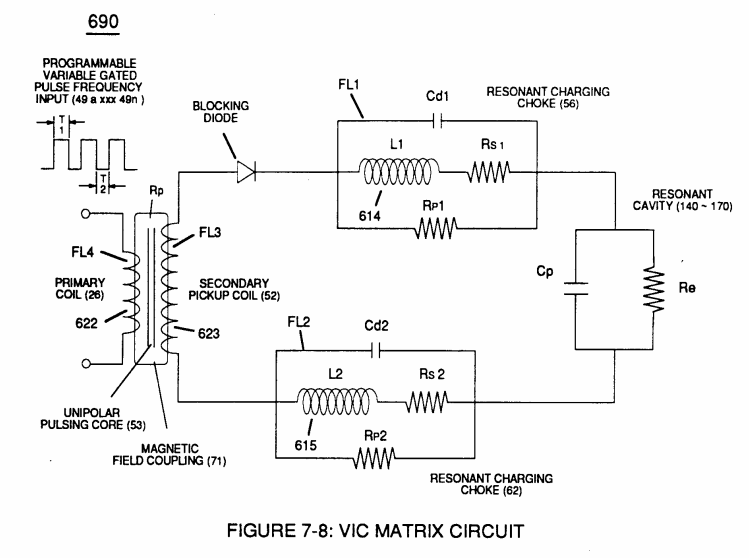
''Negative Voltage Potential" ( B- ) at one side of Water Gap (Cp) of Figure (7-8) & magnetic field (FL2) (690) of Figure (7-8) · Transformer Action
-
The figure it sits on · Differential Air-Gas Inlet Control
-
Figure 1-19B · Amp Inhibiting Circuit Vs Voltage Enhancement
-
The figure it sits on · Illustrations
-
The figure it sits on · VIC Matrix Circuit
-
Voltage Intensifier Circuit (620) of Figure (7-1) · Instant Explosion of Water
-
(700) of Figure (7-9) · Instant Explosion of Water
-
(T2) of Figure (7-8) · Instant Explosion of Water
-
(FI) of Figure (7-3b) · Instant Explosion of Water
-
(620) of Figure (7-1) · Instant Explosion of Water
-
Figure (7-8) · Resistance (Rs)
-
(620) of Figure (7-1) · Resistance (Rs)
-
(690) of Figure (7-8) · Resistance (Rs)
-
(614) of Figure (7-1) · Inductance (FL)
-
(690) of Figure (7-8) · Inductance (FL)
-
Inductor (614) of Figure (7-1) · Inductance (FL)
-
Figure (7-3) · Inductance (FL)
-
(614) of (7-1) · Inductance (FL)
-
Figure (7-1) · Capacitance (Cd)
-
(640) of Figure (7-3) · Capacitance (Cd)
-
(690) of Figure (7-8) · Capacitance (Cd)
-
(690) of Figure (7-8) · Inductance Reactance (Rs - Cd - FL)
-
"Electron Bounce" phenomenon (700) of Figure (7-9) · Inductance Reactance (Rs - Cd - FL)
-
(547) of Figure (5-9) · Inductance Reactance (Rs - Cd - FL)
-
Figure (7-8) · Inductance Reactance (Rs - Cd - FL)
-
(620) of Figure (7-1) · Inductance Reactance (Rs - Cd - FL)
-
Figure (7-3) · Multi-layer Coil
-
(690) of Figure (7-8) · Taper Resonant Capacitor (ERt)
-
Inductance Charging Effect (660) of Figure (7-5) · Transformer Action
-
(547) of Figure (5-9) · Transformer Action
-
"Electron Clustering" (Grouping/collecting negative charged particles at a given point) (700) of Figure (7-9) · Transformer Action
-
Choke-Coil (62) of Figure (7-1) · Transformer Action
-
Distributed Capacitance (Cda xxx Cdn) of Figure (7-3) · Electron Bounce Phenomenon
-
(52) of Figure (7-8) · Electron Bounce Phenomenon
-
(700) of Figure (7-9) · Electron Bounce Phenomenon
-
The figure it sits on · WFC 426 - Illustrations
-
The figure it sits on · WFC 426 - Illustrations
-
The figure it sits on · WFC 426 - Illustrations
-
(690) of Figure (7-8) · 8-2 - Traveling Voltage Wave-Guides
-
(631) of Figure (7-9) · 8-3 - Electrical Voltage-Pulse Wave-Transmission
-
(52) of Figure (7-8) · 8-3 - Electrical Voltage-Pulse Wave-Transmission
-
(Cp) of Figure (7-8) · 8-4 - State Space (Sp)
-
(620) of Figure (7-1) · 8-6 - VIC Voltage Sync-Pulse Circuit
-
(690) of Figure (7-8) · 8-6 - VIC Voltage Sync-Pulse Circuit
-
(Cp) of (7-8) · 8-6 - VIC Voltage Sync-Pulse Circuit
-
(690) of Figure (7-8) · Propagating Electrical Stress
-
"Resonant Charging Choke" (56) of Figure (7-1) · Propagating Electrical Stress
-
"bifilar" wrapped coils (Figure 7-3) · Propagating Electrical Stress
-
(620) of figure (7-1) · Voltage to Amp Differential Ratio
-
The figure it sits on · WFC 429 - Illustrations
-
The figure it sits on · The Atom Functioning as an Energy Transporter
-
The figure it sits on · VIC Switchover Circuit
Where it is named · 16
Amp Inhibiting Circuit Vs Voltage Enhancement 1×
-
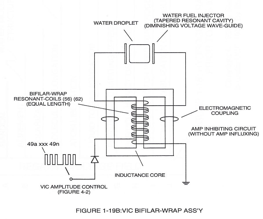
Distributed Inductance (FL1a xxx FL1n = FL2a xxx FL2n)
… piral-wrapped coils being paired together, also, causes voltage level enhancement beyond applied voltage input since the "Distributed Capacitance" (Cl xxx Cln =C2a xxx C2n) / "Distributed Inductance" (FL1a xxx FL1n = FL2a xxx FL2n) of said "Bifilar" wrapped coils encourages the compounding effect (increasing magnetic field-strength during each pulsing cycle) of electromagnetic field-strength (Rpla xxx Rpin = Rp2a xxx Rp2n) (mut …
Inductance Reactance (Rs - Cd - FL) 3×
-
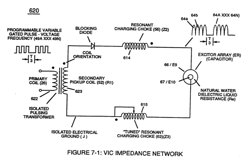
Inductor Field (L2-FL2)
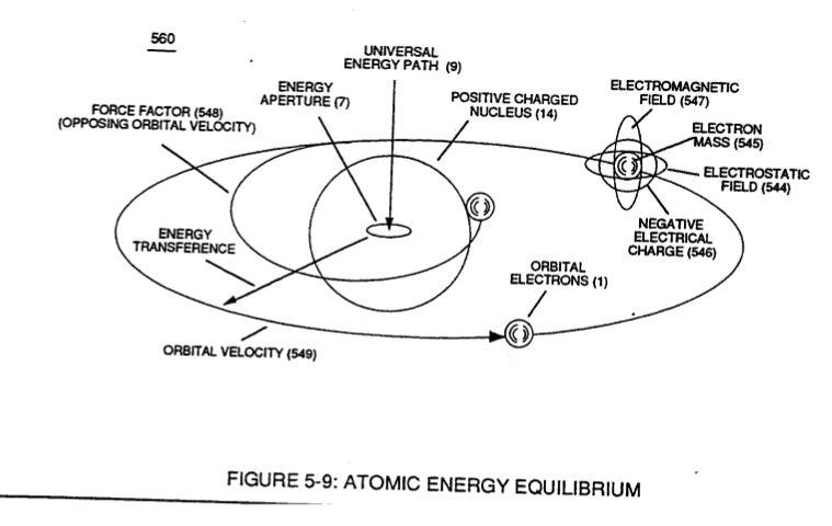
while, at the same time, Inductor Field (L2-FL2) restricts electron movement through VIC Impedance Network Circuit (620) of Figure (7-1) since Inductance Field (FL2) locks onto Electrons Magnetic Field (547) of Figure (5-9) to block the movement of electron flow toward Positive Voltage Potential (66)
-
Inductance Field (FL2)
while, at the same time, Inductor Field (L2-FL2) restricts electron movement through VIC Impedance Network Circuit (620) of Figure (7-1) since Inductance Field (FL2) locks onto Electrons Magnetic Field (547) of Figure (5-9) to block the movement of electron flow toward Positive Voltage Potential (66)
-
Inductance Fields (FL1/FL2)
... overcoming any potential loss of pulse signal due to resistive interaction (Rsl/Rs2) of either or both Inductor Cores (L1/L2) wire-material to the formation of Inductance Fields (FL1/FL2) during reoccurring pulse on-time (T1a xxx T1n).
Circuit Resistance 1×
-
inductance field strength (FL2)
(Z3) is determined by inductance field strength (FL2) and resistive value (RS2) (typically 11.6KQ) of stainless steel (sls) wire-coil (62) (L2) when being exposed to the same external magnetic coupling field strength (Rp)
Transformer Action 6×
-
Inductance Fields (FL1 - FL2 - FL3 - FL4)
... thus, allowing Inductance Fields (FL1 - FL2 - FL3 - FL4) to be aiding one another during the same sequence of pulse-time (T1) ... …
-
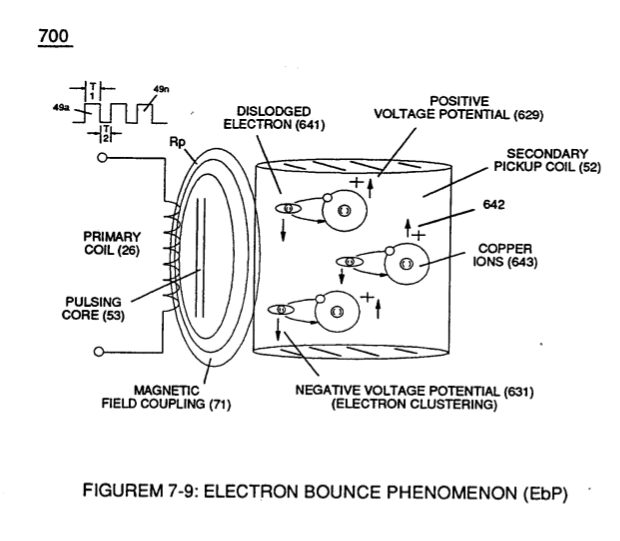
… dielectric properties of water (Re) to cause and inhibit electron flow (IF) since "electrons" magnetic field (547) of Figure (5-9) locks onto the electromagnetic fields of each energized choke coils (FL1/FL2) during Voltage Excitation (Vo -Vn) which, now, brings on and allows "Electron Bounce Phenomenon" (700) of Figure (7-9) to take place.
-
… o produce ''Negative Voltage Potential" ( B- ) at one side of Water Gap (Cp) of Figure (7-8) is accomplished by low electrical power input (Tab 38) when Choke-Coil (62) of Figure (7-1) magnetic field (FL2) (690) of Figure (7-8) during pulse on-time (49) impede "Electron-Flow" since electron mass is composed of electromagnetic matter which interacts with magnetic field strength (FL2).
-
… 7-1) magnetic field (FL2) (690) of Figure (7-8) during pulse on-time (49) impede "Electron-Flow" since electron mass is composed of electromagnetic matter which interacts with magnetic field strength (FL2).
-
''Negative Voltage Potential" ( B- ) at one side of Water Gap (Cp) of Figure (7-8) & magnetic field (FL2) (690) of Figure (7-8)
Electron Bounce Phenomenon 2×
-
Choke Coils (FL1 - FL2)
Coupling Inductance (Rp1) and (Rp2) in (690) of Figure (7-8) is further expressed in the following equation: Where, (Lt cc) is the total inductance of Choke Coils (FL1 - FL2), (L1) and (L2) are the inductance of each individual choke coil (56)(62) in series with Secondary Coil (52) Electrical Voltage Potential (700) of Figure (7-9) and being exposed to the same Voltage Tr …
-
Coefficient of Inductance (FL1/FL2)
… RR') is in balance phase of equal electrical intensity (66 = 67) of opposite polarity (positive electrical voltage potential _66 equals negative electrical Voltage potential 66 since the Voltage Coefficient of Inductance (FL1/FL2), Voltage Coefficient of Capacitance (Cd1/Cd2), and Voltage Coefficient of Resistance (Rs1/Rs2) across choke coils (L1/L2) are the same values
Propagating Electrical Stress 1×
-
Distributed Inductance (FL1a xxx FL1n - FL2a xxx FL2n)
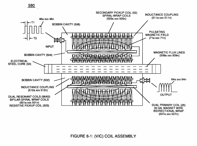
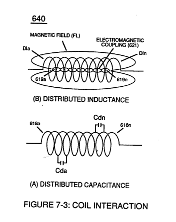
… ing Chokes 56/62) being paired together, also, causes voltage level enhancement beyond applied voltage input since the "Distributed Capacitance" (C1a xxx C1n - C2a xxx C2n) / "Distributed Inductance" (FL1a xxx FL1n - FL2a xxx FL2n) of said "bifilar" wrapped coils (Figure 7-3) as to (990) of Figure (10-3) encourages the compounding effect (increasing magnetic field-strength during each pulsing cycle) of electromagnetic field-str …
Appendix B - Glossary of Applicaiton Notes 2×
-
… ) to produce "Negative Voltage Potential" (B-) at one side of Water Gap (Cp) of Figure (7-8) is accomplished by low electrical power input (Tab 38) when Choke-Coil (62) of Figure (7-1) magnetic field (FL2) (690) of Figure (7-8) during pulse on-time (49) impede "Electron-Flow" since electron mass is composed of electromagnetic matter which interacts with magnetic field strength (FL2). …
-
… 7-1) magnetic field (FL2) (690) of Figure (7-8) during pulse on-time (49) impede "Electron-Flow" since electron mass is composed of electromagnetic matter which interacts with magnetic field strength (FL2). …