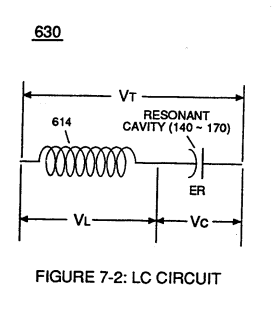
Figure (7-2)
Lc Circuit
How it is written
- (7-2) 6×
Drawings 4
-
(630) of Figure (7-2) · Inductance (FL)
-
LC circuit of Figure (7-2) · Inductance (FL)
-
Capacitor (ER) of Figure (7-2) · Capacitance Reactance
-
Captioned as this figure · WFC 426 - Illustrations
On this figure 4
Where it is named · 6
Inductance (FL) 4×
-
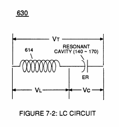
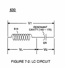
Resonant Charging Circuit (630) of Figure (7-2) being an LC Circuit is fanned when Inductor (614) of Figure (7-1) is electrically linked to Taper Capacitor (720) of Figure (7-11) in series arrangement.
-
(630) of Figure (7-2)
-
Component Reactance to D.C. pulsing transforms Inductor (614) of Figure (7-1) / Capacitor (E9/E10) of Figure (7-11) LC circuit of Figure (7-2) into an Resonant Charging Choke (614) which steps up an unipolar oscillation of an given charging frequency with the effective capacitance of a pulse-forming network (64a xxx 64n) of Figure (7-1) as …
-
LC circuit of Figure (7-2)
Capacitance Reactance 2×
-
In terms of Component Reactance, Inductors (L1/L2) should always be larger than Capacitor (ER) of Figure (7-2) in order to maximize amp restriction to enhance "Voltage Deflection" (SS' - 617a xxx 617n - RR') of Figure (7-4) and, is expressed by :
-
Capacitor (ER) of Figure (7-2)