(Vn) · also written as a run, Vna xxx Vnn
Voltage Potential
Also written High Voltage Potential of Difference · Electrical Pulse Voltage amplitude · Voltage Amplitude Burst-Time · voltage amplitude potential · Resonant Voltage Intensity · Voltage Pulse-Potential · applied voltage level · highest voltage level and 1 more
Where it is first named
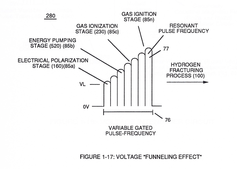
This resultant "Funneling Effect" (260), now, allows voltage amplitude (Vn) wave-form (58) to travel the length of Resonant Cavity Zone (35) from Start-Point (85a) to End-Point (85n) increasing voltage intensity (xxx VL = Vn) as parallel voltage surfaces (83/84) diminishes in size relationship (85a ~ 85n), as illustrated in (210) of Figure (17).
How it is written
- (Vn) 5×
- (Vo - Vn) 4× with (Vo) Applied Voltage Amplitude
- (Vo - 64a - 64b - 64c - Vn) 1× with (Vo) Applied Voltage Amplitude, (64) Pulse Train
- (Vo - 64a - 64b- 64c - Vn) 1× with (Vo) Applied Voltage Amplitude, (64) Pulse Train
- (Vo -64a-64b -64c - Vn) 1× with (Vo) Applied Voltage Amplitude, (64) Pulse Train
- (VO - Va - Vb - Vc - Vn) 1× with (Vo) Applied Voltage Amplitude, (Va), (Vb) VIC Voltage Enhancement Circuit, (VC) Vacuum Gap
- (Vo - Va -Vb - Vn) 1× with (Vo) Applied Voltage Amplitude, (Va), (Vb) VIC Voltage Enhancement Circuit
- (Vo -Vn) 1× with (Vo) Applied Voltage Amplitude
Vna xxx Vnn is Meyer's shorthand for a run of the same thing: Vna is the first, Vnn the last, and the x's stand for however many lie between. Every stage of the run is this one numeral.
Drawings 55
-
This established increase or decrease in Electrical Pressure (4 / 5 ), now causes Energy Aperture (7) to either enlarge or become smaller as to applied voltage amplitude (VO xxx Vn), respectively. · Energy Pumping Action
-
The figure it sits on · Differential Air-Gas Inlet Control
-
Figure (5-5) · Resonant Propagation
-
610 of Figure 6-4 · In Application of Usage
-
(57) of Figure (6-2) · In Application of Usage
-
Figure (6-4) · In Application of Usage
-
The figure it sits on · Illustrations
-
Activation Process (590) of Figure (6-2) · Voltage Intensifier Coil-Assembly
-
coil-structures (580) of Figure (6-1) · Voltage Intensifier Coil-Assembly
-
"Voltage Intensity of Opposite Potential" (600) of Figure (6-3) · Voltage Intensifier Coil-Assembly
-
The figure it sits on · WFC 425 - Illustrations
-
The figure it sits on · WFC 425 - Illustrations
-
(700) of Figure (7-9) · Instant Explosion of Water
-
Figure (7-13) · Inductance (FL)
-
(600) of Figure (6-3) · Inductance (FL)
-
(580) of Figure (6-1) · Inductance (FL)
-
(600) of Figure (6-3) · Inductance (FL)
-
(590) of Figure (6-2) · Capacitance (Cd)
-
"Electron Bounce" phenomenon (700) of Figure (7-9) · Inductance Reactance (Rs - Cd - FL)
-
(580) of Figure (6-1) · Multi-layer Coil
-
(730) of Figure (7-12) · Taper Resonant Capacitor (ERt)
-
(90) of Figure (5-5) · Capacitance Reactance
-
"Electron Clustering" (Grouping/collecting negative charged particles at a given point) (700) of Figure (7-9) · Transformer Action
-
(700) of Figure (7-9) · Electron Bounce Phenomenon
-
... causing "electron clustering" (641a xxx 641n) to take place within Copper Wire Zone (52) during pulse on- time (T1) · Electron Bounce Phenomenon
-
Traveling Electrical Voltage Wave-forms (730a - b - c) of Figure (7-12) · Electron Bounce Phenomenon
-
(see 740 of Figure 7-13) · Voltage Amplitude Switch-Off
-
(E9/10) of Figure (6-2) · Voltage Amplitude Switch-Off
-
Compressional Wave-form (B) of Figure (7-12) · Voltage Amplitude Switch-Off
-
The figure it sits on · Mode of Operability
-
The figure it sits on · WFC 426 - Illustrations
-
The figure it sits on · 8-1 - Propagating "Resonant Action" By Voltage Tickling of State Space
-
(730A) of Figure (7-12) · 8-2 - Traveling Voltage Wave-Guides
-
(580) of Figure (6-1) (WFC memo 425) · 8-2 - Traveling Voltage Wave-Guides
-
(780A) Figure (8-2) · 8-2 - Traveling Voltage Wave-Guides
-
(570) of Figure (7-12) · 8-2 - Traveling Voltage Wave-Guides
-
Figure (8-6) · 8-2 - Traveling Voltage Wave-Guides
-
(90) of Figure (5-5) · 8-2 - Traveling Voltage Wave-Guides
-
Figure (8-2) · 8-2 - Traveling Voltage Wave-Guides
-
(631) of Figure (7-9) · 8-3 - Electrical Voltage-Pulse Wave-Transmission
-
(780 B) of Figure (8-2) · 8-4 - State Space (Sp)
-
(780 A/B/C) of Figure (8-2) · 8-4 - State Space (Sp)
-
(730) of Figure (7-12) · 8-5 - Energy Vectoring (Ev)
-
Clipped Voltage Wave-form (780C) of Figure (8-2) · 8-5 - Energy Vectoring (Ev)
-
The figure it sits on · 8-6 - VIC Voltage Sync-Pulse Circuit
-
(820B) of Figure (8-6) · 8-7 - Application of Usage
-
(730C) of Figure (7-12) · 8-7 - Application of Usage
-
(820C) of Figure (8-6) · 8-7 - Application of Usage
-
(730A) of Figure (7-12) · 8-7 - Application of Usage
-
Figure (820A) of Figure (8-6) · 8-7 - Application of Usage
-
The figure it sits on · WFC 427 Illustrations
-
The figure it sits on · WFC 427 Illustrations
-
The programmable pulse-frequency (49a xxx 49n) of Figure (10-1) input is simply adjusted to tune-in to the dielectric property of the Water Molecule. · Propagating Electrical Stress
-
(580) of Figure (6-1) · Voltage to Amp Differential Ratio
-
(970) of Figure (10-1) · VIC Switchover Circuit
Where it is named · 19
Funneling Effect 1×
-
This resultant "Funneling Effect" (260), now, allows voltage amplitude (Vn) wave-form (58) to travel the length of Resonant Cavity Zone (35) from Start-Point (85a) to End-Point (85n) increasing voltage intensity (xxx VL = Vn) as parallel voltage surfaces (83/84) diminishes in size relationship (85a ~ 85n), as illustrated in (210) of Figure (17).
In Application of Usage 1×
-
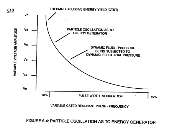
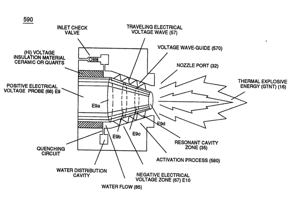
… applied traveling voltage wave-form (57) of Figure (6-2) of opposite electrical polarity (E9-66/ ElO-67) initiates the voltage-triggering process (600) of Figure (6-3) once maximum voltage deflection (VO - Va - Vb - Vc - Vn) of Figure (6-4) is achieved at Activation-Point (E9d) of Figure (6-2) ... releasing thermal Explosive Energy (gtnt) from the atomic level of the water molecule.
Water Fuel Injector 1×
-
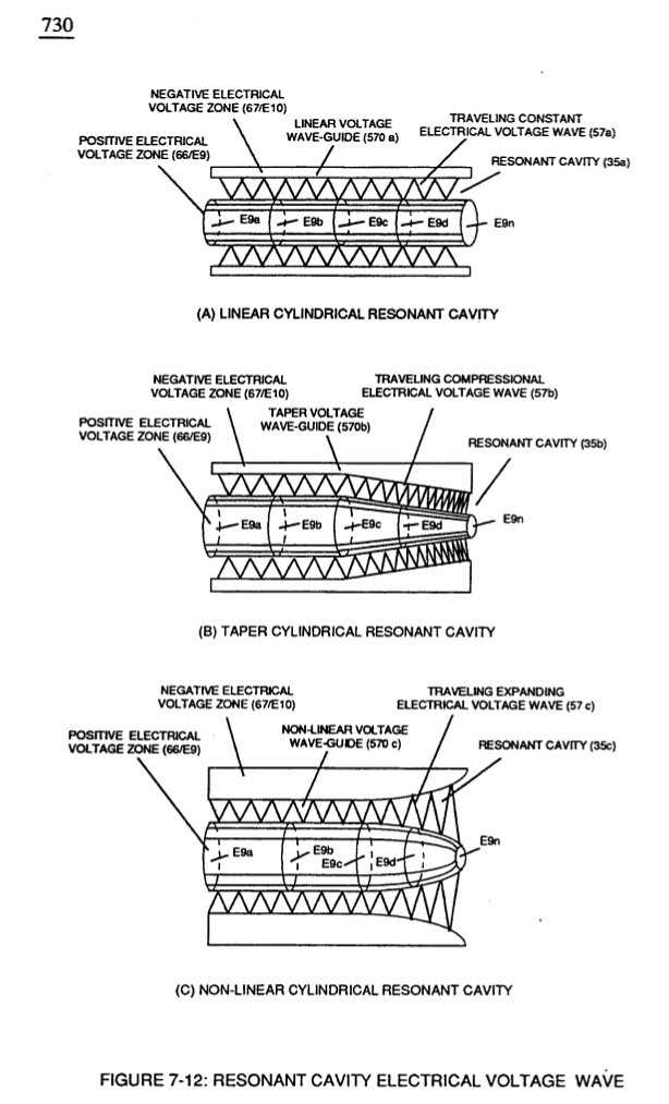
At each progressive point of diminishing circumference surface-area (E9a - b - c - d - E9n) voltage amplitude intensity increases (Vna - b - c - d - Vnn) uniformly, as illustrated in (600) of Figure (6-3) as to Travelling Voltage Wave-forms (730a - b - c) of Figure (7-12), see WFC Memo (426).
Inductance (FL) 1×
-
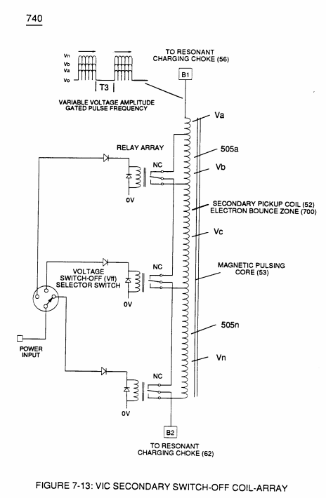
Component Interaction promotes Component Reactance during D.C. pulsing operations while allowing variable voltage amplitude (Vo - Va -Vb - Vn) of Figure (7-13) to be attenuated independently of Voltage Pulse frequency (49a xxx 49n), as so illustrated in (600) of Figure (6-3).
In-Line Circuit Components 1×
-
highest voltage level (Vn)
... determining voltage swing from highest voltage level (Vn) to volts switch-off point (Vff), and establishing Impedance (FL) which minimizes heat loss of electrical input power (49) by impairing electron movement.
Transformer Action 2×
-
Voltage Potential (Vo - Vn)
Magnetic Induction (71a - 71n) is determined by Inductance Permeability (μL) of core material (53) along with VIC circuit geometry ability to step up Voltage Potential (Vo - Vn) by way of "Transformer Action", and is expressed in the following equations:
-
Voltage Excitation (Vo -Vn)
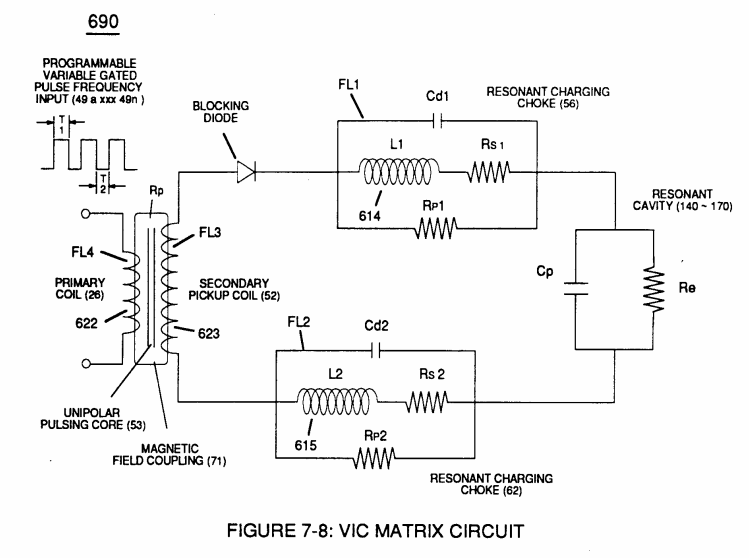
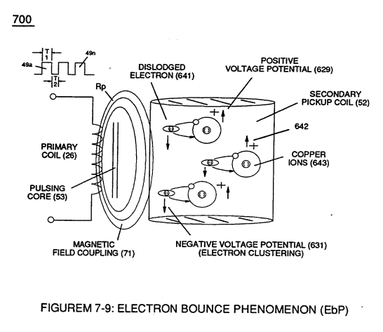
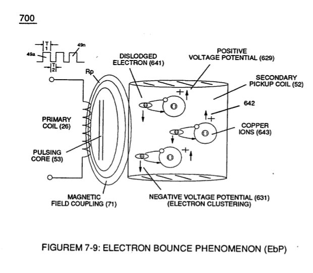
… to cause and inhibit electron flow (IF) since "electrons" magnetic field (547) of Figure (5-9) locks onto the electromagnetic fields of each energized choke coils (FL1/FL2) during Voltage Excitation (Vo -Vn) which, now, brings on and allows "Electron Bounce Phenomenon" (700) of Figure (7-9) to take place.
Electron Bounce Phenomenon 4×
-
High Voltage Potential of Difference (Vo - Vn)
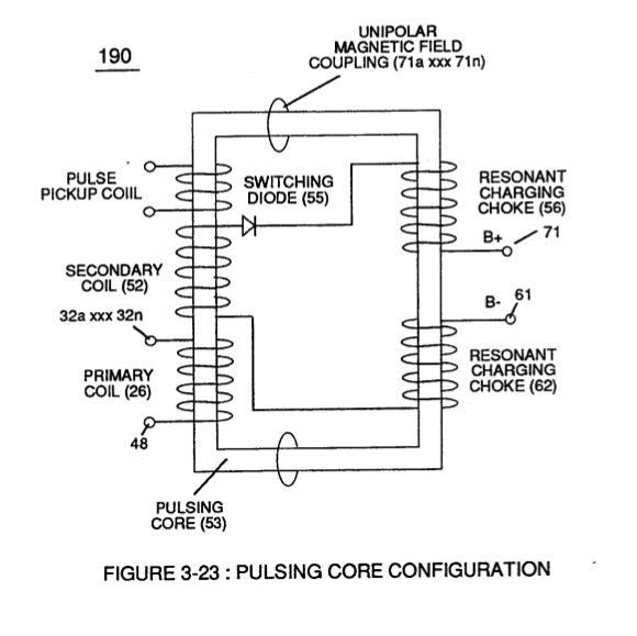
High Voltage Potential of Difference (Vo - Vn) (SS' - 617 -RR') is accomplished when magnetic flux lines of force (71a xx 71n) (Rp) emanating away from closed-loop magnetic pulsing core (53) of Figure (190) penetrates Inductance coil-windings (52 …
-
Voltage Potential (Vo - Vn)
Sustaining and maintaining the resultant induced Voltage Potential (Vo - Vn) without "Electron Discharged" (inhibiting electron flow) through Choke Coil (62) while, at the same time, inhibiting (preventing) any additional or other electrons from entering into Secondary copper wire-zone (52) by way of Choke Coil (56) is herein called "Electron Bounce Phenomenon" (EbP), as illustrated in (700) of Figure (7-9).
-
Voltage Potential (Vo - Vn)
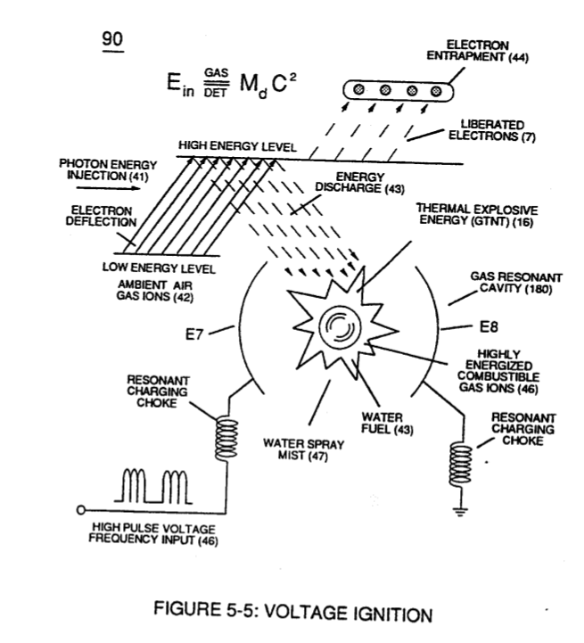
… icient of Inductance (F11/F12), Voltage Coefficient of Capacitance (Cd1/Cd2), Voltage Coefficient of Resistance (Rs1/Rs2), and Dielectric Coefficient of Water resistance (Re) allows Voltage Potential (Vo - Vn) of opposite electrical polarity to perform work (SS' _ 617 _ RR') without amp influxing, thus, not allowing the introduction of electron flow into Hydrogen Fracturing Process (90) of Figure (5-5) dur …
-
Resonant Voltage Intensity (Yo -Vn)
... therefore, producing a physical force-yield (Fy) during gas-ignition (70) of Figure (4-5) which is directly related to the liquid volume of water (85) per injection cycle and applied Resonant Voltage Intensity (Yo -Vn), as illustrated in (590) of Figure (6-2) as to (90) of Figure (5-5).
Mode of Operability 2×
-
Voltage Potential (Vn)
The established "mode-of-operability" of VIC Coil Assembly (580) of Figure (6-1), now, allows Voltage Potential (Vn) of opposite voltage polarity (66/SS' - 67/RR') to increase and be attenuated up to and beyond 20 Kilovolts while inhibiting and restricting amp leakage in the milliamperes range
-
... increasing Thermal Explosive Energy-yield (gtnt) to higher energy-levels (gtnta xxx gtntn) beyond applied excitation voltage (Vn) by simply altering Voltage Surfaces (35b/35c) as in reference to Linear Voltage Surfaces (35a), as illustrated in (730) of Figure (7-12).
8-2 - Traveling Voltage Wave-Guides 2×
-
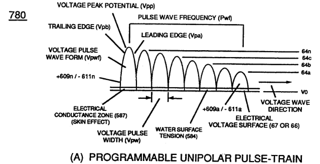
… 6-1) (WFC memo 425) ability to inhibit amp "influxing" (Electron Bounce Phenomenon EbP) during pulsing operations (49a xx 49n) allows voltage amplitude of pulse-frequency potential (T1a xxxT1n) as to (Vo -64a-64b -64c - Vn) of (780A) Figure (8-2) to be applied across cross-sectional circular-ring water bath (85) (donut shape) to cause Voltage Wave-Form (57) of Figure (6-2) to travel the entire longitudinal length of wat …
-
voltage amplitude potential (Vo - 64a - 64b - 64c - Vn)
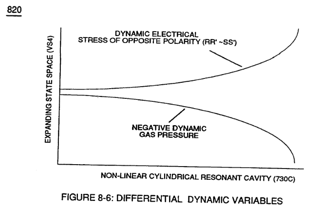
... thereby, maintaining voltage amplitude potential (Vo - 64a - 64b - 64c - Vn) of Figure (8-6) without experiencing amp arc-over across Water-Gap (616) in any appreciable amount
8-3 - Electrical Voltage-Pulse Wave-Transmission 1×
-
Electrical Pulse Voltage amplitude (Vo - 64a - 64b- 64c - Vn)
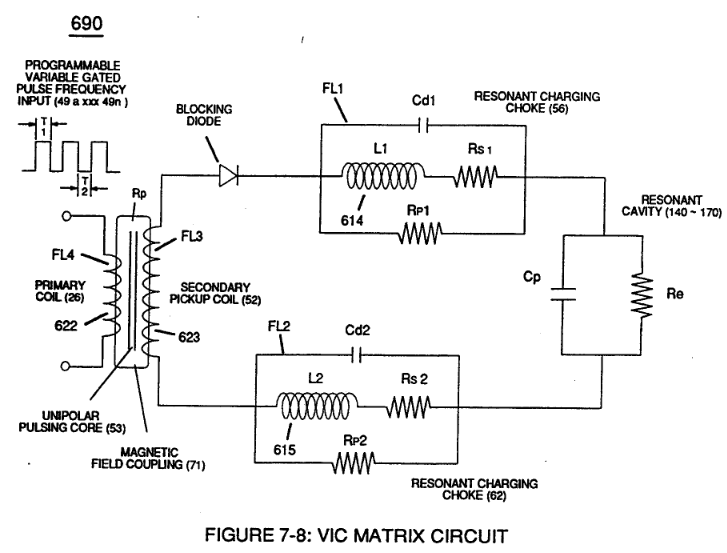
Electrical Voltage-Pulse Wave-Transmission (583a xxx 583n), now formed, occurs along Electrical Conductance Zone (587) since applied Electrical Pulse Voltage amplitude (Vo - 64a - 64b- 64c - Vn) is time responsive (T1/T2a - T3 – T1/T2n) to incoming gated Voltage Pulse Frequency (49a xxx - 1'3 - xxx 49n).
8-4 - State Space (Sp) 1×
-
Voltage Amplitude Burst-Time (Vpa - Vn -Vpb)
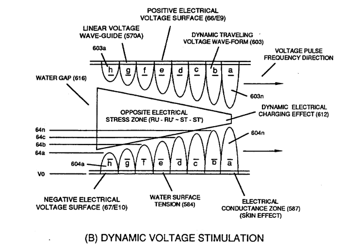
The newly formed Opposite Electrical Attraction Force (RR' - SS') intensity is directly related to the applied Voltage Amplitude Burst-Time (Vpa - Vn -Vpb) as to the Voltage Burst-Frequency (49a xxx 49n) as to Voltage Peak Excursion Point "P" at the height of Unipolar Voltage Pulse Wave (583/602) which, in turns, determines maximum Voltage Peak-Potentia …
Propagating Electrical Stress 1×
-
Voltage Pulse-Potential (Va xxx Vn/49a xxx 49n)
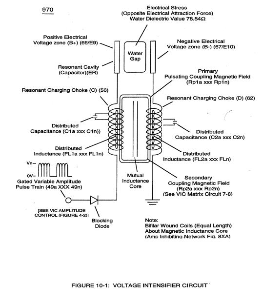
… The length and diameter size of the copper-wire spiral wrapped coil (56/62) of Figure (10-1) being paired together and electrically energized in conjunction with applied Voltage Pulse-Frequency determines how much "Amp Leakage" will occur across capacitor Gap (Cp) while "Voltage Pulse-Potential" (Va xxx Vn/49a xxx 49n) of "Opposite polarity" (B+/B-) is/are allowed to be applied across "Electrical Voltage Plates" (Voltage-Zones) (66/67).
VIC Switchover Circuit 1×
-
applied voltage level (Vn)
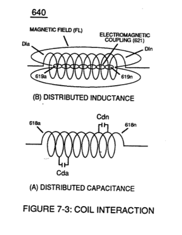
While, the distributed capacitance (Cda xxx Cdn) of each coil experiencing inductance coupling (619) elevates applied voltage level (Vn) to a higher voltage amplitude (increasing voltage intensity) required to deflect the bipolar water molecule to a given or pre-selected distance.