patent · US11086013B2
Micro-optics for imaging module with multiple converging lenses per channel
10 August 2021
Page 1 — bibliographic record
( 12) United States Patent ( 10) Patent No .: US 11,086,013 B2 Pacala et al . (45) Date of Patent : Aug. 10 , 2021 ( 54 ) MICRO -OPTICS FOR IMAGING MODULE ( 56 ) References Cited
WITH MULTIPLE CONVERGING LENSES
PER CHANNEL U.S. PATENT DOCUMENTS ( 71 ) Applicant: Ouster, Inc., San Francisco , CA ( US ) 4,003,660 A 1/1977 Christie , Jr. et al .
( 72 ) Inventors : Angus Pacala , San Francisco , CA (US ); (Continued ) Mark Frichtl , San Francisco, CA (US ) FOREIGN PATENT DOCUMENTS ( 73 ) Assignee : OUSTER, INC . , San Francisco, CA CN 1918427 2/2007 (US ) CN 101413905 4/2009 ( * ) Notice: Subject to any disclaimer, the term of this (Continued ) patent is extended or adjusted under 35
U.S.C. 154 ( b ) by 257 days . OTHER PUBLICATIONS ( 21 ) Appl. No .: 15 /979,295 European Patent Office; Extended European Search Report received in European Application No. 16865297.2 , dated Jun . 11 , 2019 ; 9 (22 ) Filed : May 14 , 2018 pages.
( Continued )
US 2018/0329062 A1 Nov. 15 , 2018 Primary Examiner Luke D Ratcliffe Related U.S. Application Data (74 ) Attorney, Agent, or Firm — Kilpatrick Townsend & Stockton LLP ( 60 ) Provisional application No. 62 / 506,449 , filed on May 15 , 2017 , provisional application No. 62 / 506,437 , (57) ABSTRACT (Continued ) Embodiments describe optical imagers that include one or ( 51 ) Int . CI . more micro -optic components. Some imagers can be passive GOIS 17/10 ( 2020.01) imagers that include a light detection system for receiving GO2B 27/30 ( 2006.01) ambient light from a field . Some imagers can be active (Continued ) imagers that include a light emission system in addition to the light detection system . The light emission system can be (52) U.S. Ci. configured to emit light into the field such that emitted light CPC GOIS 17/10 (2013.01 ) ; GOIS 7/486 is reflected off surfaces of an object in the field and received (2013.01 ) ; GOIS 7/4813 ( 2013.01 ) ; by the light detection system . In some embodiments, the ( Continued ) light detection system and / or the light emission system ( 58 ) Field of Classification Search includes micro -optic components for improving operational CPC . GO2B 27/22 ; GO2B 3/00 ; GO2B 5/00 ; G02B performance.
See application file for complete search history. 38 Claims , 36 Drawing Sheets Light Detection
System 200
Bulk receiver Micro - Optic Rx
202 Layer 211 Layer 204
Light Cone
Optic Rx
Apertures
206 Collimating 216
Lenses 234 Optical
Filter 218
Page 2
Related U.S. Application Data 7,091,462 B2 8/2006 Wilson et al .
filed on May 15 , 2017 , provisional application No. 7,170,542 B2 1/2007 Hanina et al . 62/506,445, filed on May 15 , 2017 , provisional ap 7,196,301 B2 3/2007 Thomas et al .
plication No. 62/ 515,291 , filed on Jun. 5 , 2017 . 7,345,271 B2 3/2008 Boehlau et al .
(51 ) Int. Ci . 7,433,042 B1 * 10/2008 Cavanaugh GO1J 3/02 GOIS 7/486 ( 2020.01 ) 356/419 GO2B 27/00 ( 2006.01 ) 7,808,706 B2 10/2010 Fadel et al . GO2B 27/09 7,969,558 B2 6/2011 Hall ( 2006.01 ) 8,013,983 B2 9/2011 Lin et al .
GOIS 17/42 ( 2006.01 ) 8,089,618 B2 1/2012 Yang GOIS 7/481 ( 2006.01 ) 8,130,367 B2 3/2012 Stettner et al. GOIS 7/4863 ( 2020.01) D659,030 S 5/2012 Anselment et al . GOIS 7/4865 ( 2020.01 ) 8,319,949 B2 11/2012 Cantin et al . HOIL 31/0232 ( 2014.01 ) 8,330,840 B2 12/2012 Lenchenkov
HOIL 31/0216 ( 2014.01 ) 8,384,997 B2 2/2013 Shpunt et al . GOIS 17/931 ( 2020.01 ) 8,494,252 B2 7/2013 Freedman et al . GOIS 17/89 ( 2020.01 ) 8,633,384 B1 1/2014 Shotey et al . HOIL 27/146 ( 2006.01 ) 8,675,181 B2 3/2014 Hall HOIL 31/02 8,717,488 B2 5/2014 Shpunt et al . ( 2006.01 ) 8,742,325 B1 6/2014 Droz et al .
GOIS 17/08 ( 2006.01 ) 8,743,176 B2 6/2014 Stettner et al . H04B 10/50 ( 2013.01 ) 8,761,495 B2 6/2014 Freedman et al . H04B 10/67 ( 2013.01 ) 8,767,190 B2 7/2014 Hall H04B 10/69 ( 2013.01 ) 8,829,406 B2 9/2014 Akerman et al . H04B 10/80 ( 2013.01 ) 8,836,922 B1 9/2014 Pennecot et al .
HOIL 27/144 ( 2006.01 ) 9,041,915 B2 5/2015 Earhart et al . HOIL 31/107 ( 2006.01 ) 9,063,549 B1 6/2015 Pennecot et al . GO2B 5/20 ( 2006.01 ) 9,071,763 B1 6/2015 Templeton et al . ( 52 ) U.S. Cl. 9,086,273 B1 7/2015 Gruver et al .
CPC GOIS 7/4815 ( 2013.01 ) ; GOIS 7/4816 9,157,790 B2 10/2015 Shpunt et al . ( 2013.01 ) ; GOIS 7/4817 (2013.01 ) ; GOIS 9,164,511 B1 10/2015 Ferguson et al . 7/4863 (2013.01 ) ; G01S 7/4865 ( 2013.01 ) ; 9,176,051 B2 11/2015 Mappes et al .
GOIS 17/08 (2013.01 ) ; GOIS 17/42 ( 2013.01 ) ; 9,285,464 B2 3/2016 Pennecot et al . GOIS 17/89 ( 2013.01 ) ; GOIS 17/931 9,285,477 B1 3/2016 Smith et al. ( 2020.01 ) ; GO2B 27/0037 ( 2013.01 ) ; GO2B 9,299,731 B1 3/2016 Lenius et al. 27/0955 ( 2013.01 ) ; GO2B 27/30 ( 2013.01 ) ; 9,366,573 B2 6/2016 Geelen et al . HOIL 27/1446 (2013.01 ) ; HOIL 27/14643 9,368,936 B1 6/2016 Lenius et al . (2013.01 ) ; HOIL 31/02027 ( 2013.01 ) ; HOIL 9,369,689 B1 6/2016 Tran et al .
31/02162 (2013.01 ) ; HOIL 31/02164 9,425,654 B2 8/2016 Lenius et al.
(2013.01 ) ; HOIL 31/02165 ( 2013.01 ) ; HOIL 9,435,891 B2 9/2016 Oggier 31/02325 (2013.01 ) ; HOIL 31/02327 9,470,520 B2 10/2016 Schwarz et al . ( 2013.01 ) ; HOIL 31/107 ( 2013.01 ) ; H04B 9,489,601 B2 11/2016 Fairfield et al . 10/503 (2013.01 ) ; H04B 10/675 ( 2013.01 ) ; 9,525,863 B2 12/2016 Nawasra et al .
H04B 10/6973 (2013.01 ) ; H04B 10/801 9,551,791 B2 1/2017 Van Den Bossche et al .
1/2018 Lenius et al.
( 56 ) References Cited 9,935,514 B1 4/2018 Lenius et al.
4,358,851 A 11/1982 Scifres et al . 10,066,990 B2 9/2018 Rosen et al . 4,634,272 A 1/1987 Endo 10,183,541 B2 1/2019 Van Den Bossche et al . 4,676,599 A 6/1987 Cruz 10,222,458 B2 3/2019 Pacala et al . 4,702,600 A 10/1987 Handrich et al . 10,222,475 B2 3/2019 Pacala et al . 4,744,667 A 5/1988 Fay et al . 10,663,586 B2 5/2020 Pacala et al . 4,851,664 A 7/1989 Rieger 2003/0006676 Al 1/2003 Smith et al. 5,084,596 A 1/1992 Borsh 2003/0047752 A1 3/2003 Campbell et al . 5,267,016 A 11/1993 Meinzer et al . 2004/0061502 Al 4/2004 Hasser 5,288,992 A 2/1994 Fohl 2004/0223071 Al 11/2004 Wells et al . 4/1998 Kessler et al . 2005/0030409 Al 2/2005 Matherson et al . 5,745,153 A 2005/0035474 Al 2/2005 Itoh 5,982,552 A 11/1999 Nakama et al . 2006/0244851 A1 11/2006 Cartlidge
6,374,024 B1 4/2002 Iijima 2007/0228262 Al 10/2007 Cantin et al . 6,414,746 B1 7/2002 Stettner et al . 2008/0153189 Al 6/2008 Plaine et al . 6,433,934 B1 8/2002 Reznichenko et al . 2009/0016642 Al 1/2009 Hart 6,690,019 B2 2/2004 Stettner et al . 2009/0040629 A1 2/2009 Bechtel et al. 6,721,262 B1 4/2004 Jordache et al . 2009/0179142 A1 7/2009 Duparre et al .
Page 3
( 56 ) References Cited 2016/0291134 Al
10/2016 Schwarz et al.
2009/0295910 A1 12/2009 Mir et al . 2017/0078026 Al 3/2017 Brilman et al . 2010/0008588 A1 1/2010 Feldkhun et al . 2017/0146640 A1 5/2017 Hall et al . 2010/0020306 A1 1/2010 Hall 2017/0219426 Al 8/2017 Pacala et al . 2010/0110275 A1 5/2010 Mathieu 2017/0219695 A1 8/2017 Hall et al . 2010/0123893 A1 5/2010 Yang 2017/0269197 A1 9/2017 Hall et al . 2010/0204964 Al 8/2010 Pack et al . 2017/0269198 Al 9/2017 Hall et al . 2011/0025843 Al 2/2011 Oggier et al . 2017/0269209 Al 9/2017 Hall et al . 2011/0032398 Al 2/2011 Lenchenkov 2017/0269215 A1 9/2017 Hall et al . 2011/0037849 Al 2/2011 Niclass et al . 2017/0289524 Al 10/2017 Pacala et al . 2011/0116262 Al 5/2011 Marson 2017/0350983 Al 12/2017 Hall et al . 2011/0216304 A1 9/2011 Hall 2018/0003823 Al 1/2018 Yan 2011/0266022 A1 11/2011 Jafari 2018/0059222 A1 * 3/2018 Pacala GO1S 17/89 2012/0044476 Al 2/2012 Earhart et al . 2018/0106900 Al 4/2018 Droz et al . 2012/0140109 A1 6/2012 Shpunt et al. 2018/0109061 Al 4/2018 Pardhan et al . 2012/0154914 A1 6/2012 Moriguchi et al. 2018/0118041 A1 5/2018 Lenius et al . 2012/0170029 Al 7/2012 Azzazy et al . 2018/0123412 A1 5/2018 Karplus et al . 2012/0182464 A1 7/2012 Shpunt et al. 2018/0136321 A1 * 5/2018 Verghese GO1S 7/487 2012/0287417 A1 11/2012 Mimeault 2018/0152691 A1 5/2018 Pacala 2012/0320164 Al 12/2012 Lipton 2018/0180720 A1 6/2018 Pei et al . 2013/0044310 A1 2/2013 Mimeault 2018/0191967 Al 7/2018 Kester 2013/0141549 Al 6/2013 Beers et al . 2018/0209841 A1 7/2018 Pacala 2013/0206967 A1 8/2013 Shpunt et al. 2018/0217236 A1 8/2018 Pacala 2013/0294089 A1 11/2013 Freedman et al . 2018/0267148 Al 9/2018 Buettner et al . 2013/0300840 A1 11/2013 Borowski 2018/0284228 A1 10/2018 LaChapelle 2013/0325241 A1 12/2013 Lombrozo et al . 2018/0286909 Al 10/2018 Eichenholz et al . 2014/0111812 Al 4/2014 Baeg et al. 2018/0299554 Al 10/2018 van Dyck 2014/0118335 Al 5/2014 Gurman 2019/0041498 A1 2/2019 Droz et al .
2014/0153001 Al 6/2014 Chayat et al. FOREIGN PATENT DOCUMENTS
2014/0168631 A1 6/2014 Haslim et al . CN 102640037 8/2012 2014/0176933 A1 6/2014 Haslim et al . DE 102015217908 3/2017 2014/0211194 Al 7/2014 Pacala et al . EP 1193539 4/2002 2014/0224792 Al 8/2014 Beneke EP 2110699 10/2009 2014/0269796 A1 9/2014 Geske et al . EP 2124069 11/2009 2014/0285628 A1 9/2014 Shpunt et al. EP 3002548 4/2016 2014/0291491 A1 10/2014 Shpunt et al . EP 3045935 A1 7/2016 2014/0293263 Al 10/2014 Justice et al . EP 3002548 9/2016 2014/0313519 Al 10/2014 Shpunt et al . EP 3316000 A1 5/2018 2014/0320843 Al 10/2014 Streuber et al . JP 036407 1/1991 2014/0375977 Al 12/2014 Ludwig et al. JP 0749417 2/1995 2014/0376092 Al 12/2014 Mor KR 20130111130 10/2013 2015/0002636 Al 1/2015 Brown WO 2015025497 2/2015 2015/0055117 A1 2/2015 Pennecot et al. WO 2015052616 4/2015 2015/0131080 A1 5/2015 Retterath et al . WO 2016116733 7/2016 2015/0184999 A1 7/2015 Stettner WO 2016125165 8/2016 2015/0192677 A1 7/2015 Yu et al . WO 2017132704 8/2017 2015/0260630 A1 9/2015 Yacoub et al . WO 2018065426 Al 4/2018 2015/0260830 A1 9/2015 Ghosh et al . WO 2018065427 A1 4/2018 2015/0292948 A1 10/2015 Goldring et al . WO 2018065428 A3 4/2018 2015/0293224 A1 10/2015 Eldada et al . WO 2018065429 Al 4/2018 2015/0316473 Al 11/2015 Kester et al . WO 2018122415 A1 7/2018 2015/0355470 A1 12/2015 Herschbach WO 2018197441 A1 11/2018
2015/0379371 Al 12/2015 Yoon et al . OTHER PUBLICATIONS
2016/0047895 A1 2/2016 Dussan PCT /US2018 /032601 , “ International Search Report and Written 2016/0047896 Al 2/2016 Dussan Opinion ”, dated Sep. 21 , 2018 , 16 pages . 2016/0047897 A1 2/2016 Dussan PCT /US2018 /032601 , “ Invitation to Pay Additional Fees and, 2016/0047898 A1 2/2016 Dussan Where Applicable, Protest Fee ” , dated Jul. 26 , 2018 , 2 pages . 2016/0047899 Al 2/2016 Dussan “ HDL - 32E ” , User's Manual 2010 , Velodyne Lidar, Inc. , Available 2016/0047900 A1 2/2016 Dussan online at: https://www.yumpu.com/en/document/view/11661149/
2016/0047903 Al 2/2016 Dussan hdl - 32e -manual-velodyne - lidar, Aug. 2016 , 28 pages . 2016/0049765 Al 2/2016 Eldada “ HDL - 32E ” , Data Sheet 2010 , Velodyne Lidar, Inc. , Available 2016/0097858 A1 4/2016 Mundhenk et al . online at: http://pdf.directindustry.com/pdf/velodynelidar/hdl-32e 2016/0150963 A1 6/2016 Roukes et al . datasheet / 182407-676098.html, 2017 , 3 pages . 2016/0161600 A1 6/2016 Eldada et al . “ HDL -32E ” , Velodyne Lidar, Inc. , Available online at: http : //www . 2016/0218727 A1 7/2016 Maki velodynelidar.com/hdl-32e.html, Dec. 6 , 2017 , 3 pages . 2016/0254312 Al 9/2016 Lee et al . “ HDL -64E ”, Velodyne Lida, Inc. , Available online at: http : //www. 2016/0265902 A1 9/2016 Nawasra et al . velodynelidar.com/hdl-64e.html, Dec. 6, 2017 , 12 pages . 2016/0274221 Al 9/2016 Wu et al . “ HDL -64E S2 ” , Data Sheet , Velodyne Lidar, Inc. , Available online 2016/0282453 Al 9/2016 Pennecot et al . at: http://velodynelidar.com/lidar/products/brochure/HDL-64E% 2016/0282468 A1 9/2016 Gruver et al . 2012 % 20datasheet_2010_lowres.pdf, 2017 , 2 pages .

Page 4
( 56 ) References Cited Guerrieri et al . , “ Two -Dimensional SPAD Imaging Camera for Photon Counting ”, IEEE Photonics Journal, vol . 2 , No.5 , Oct. 2010 ,
OTHER PUBLICATIONS pp . 759-774 .
Itzler et al . , “ Geiger-Mode Avalanche Photodiode Focal Plane “ HDL -64E S2 and S2.1" , Velodyne Lidar, Inc. , User's Manual and Arrays for Three -dimensional Imaging LADAR ” , Proc of SPIE . vol . Programming Guide, Firmware version 4 , 2007 , 43 pages . 7808 , 2010 , pp . 78080C - 1-78080C - 14 . “ HDL -64E S3 ” , Velodyne Lidar, Inc. , S3 User's Manual and Kilpela et al . , “ Precise Pulsed Time-of - Flight Laser Range Finder Programming Guide revision J , Dec. 2017 , 54 pages . for Industrial Distance Measurements ” , Review of Scientific Instru " Puck Hi - Res ” , Velodyne Lidar, Inc. , Available online at: http // ments, vol . 72 , No. 4 , Apr. 2001 , pp . 2197-2202 . www.velodynelidar.com/vlp-16-hi-res.html, Dec. 13 , 2017 , 2 pages . PCT/US2017 /039306 , “ International Search Report and Written
“ Puck Hi - Res Data Sheet ” , Velodyne Lidar, Inc. , Sep. 2016 , 2 PCT /US2017 /039306 , “ Invitation to Pay Additional Fees and, pages. Where Applicable , Protest Fee ” , dated Aug. 31 , 2017 , 2 pages. “ Puck Hi - Res User Manual ” , Velodyne Lidar, Inc. , Sep. 2016 , 49 PCT /US2017 /048379 , “ International Search Report and Written pages. Opinion ” , dated Nov. 2 , 2017 , 12 pages . “ Puck Lite ” , Velodyne Lidar, Inc. , Our Lightest Sensor Ever, PCT/US2018 /032601 , “ International Preliminary Report on Pat Available online at: http://velodynelidar.com/vlp-16-lite.html, Apr. entability ”, dated Nov. 28 , 2019 , 13 pages . 2016, 2 pages. SG11201910605R , “ Written Opinion ” , dated May 16 , 2020 , 6 pages.
" Puck Lite Data Sheet ” , Velodyne Lidar, Inc. , Feb. 2016 , 2 pages . U.S. Appl. No. 15 /979,253 , “ Final Office Action ” , dated Aug. 4 , “ Puck Lite User Manual” , Velodyne Lidar, Inc. , Feb. 2016 , 49 2020, 9 pages .
pages. IN201947048756 , “ First Examination Report ” , dated Dec. 2 , 2020 , “ Ultra Puck VLP - 32C ” , Velodyne Lidar, Inc. , Available online at: 6 pages.
http://velodynelidar.com/vip-32c.html, Nov. 2017 , pages. U.S. Appl. No. 15 /979,253 , “ Non -Final Office Action ” , dated Feb. “ Velodyne LiDAR Puck ” , Velodyne Lidar, Inc. , Available online at: 19, 2021 , 7 pages.
http://www.velodynelidar.com/vlp-16.html, Dec. 6 , 2017 , 48 pages . U.S. Appl. No. 15 /979,266 , “ Non - Final Office Action ” , dated Feb. “ Velodyne LiDAR Puck ” , Velodyne Lidar, Inc. , User's Manual and 22, 2021 , 16 pages.
Programming Guide, 2014 , 49 pages . CN202010078057.9 , " Office Action ”, dated Nov. 9 , 2020 , 9 pages . “ VLP - 16 ” , Velodyne Lidar, Inc. , Puck, Real Time 3D Lidar Sensor, EP18802192.7 , “ Extended European Search Report” , dated Nov. 2014 , 2 pages . 12, 2020 , 11 pages.
U.S. Appl. No. 15 /979,235 , “ Non - Final Office Action ”, dated Jul. U.S. Appl. No. 15 /979,253 , “ Corrected Notice of Allowability ” , 23 , 2018, 5 pages. dated Dec. 1 , 2020 , 2 pages.
U.S. Appl. No. 15 /979,235 , “ Notice of Allowance ” , dated Dec. 19 , U.S. Appl. No. 15 /979,253 , “ Corrected Notice of Allowability ” , 2018 , 5 pages . dated Dec. 22, 2020, 2 pages.
U.S. Appl. No. 15 / 979,253 , “ Non - Final Office Action ” , dated Mar. U.S. Appl. No. 15 /979,253 , “ Corrected Notice of Allowability ” , 20, 2020, 10 pages. dated Jan. 15 , 2021 , 2 pages.
U.S. Appl. No. 16 /245,909 , “ Non - Final Office Action ”, dated Sep. U.S. Appl. No. 15 /979,253 , “ Corrected Notice of Allowability ” , 18, 2019, 6 pages. dated Jan. 8, 2021 , 2 pages.
U.S. Appl. No. 16/245,909 , “ Notice of Allowance ” , dated Jan. 14 , U.S. Appl. No. 15 / 979,253 , " Non - Final Office Action ” , dated Oct. 2020 , 5 pages . 23 , 2020 , 12 pages.
AU2018269000 , “ First Examination Report” , dated Jun . 22 , 2020 , U.S. Appl. No. 15 / 979,253 , " Notice of Allowance ” , dated Nov. 13 , 5 pages. 2020, 7 pages.
Bronzi et al . , “ 100 000 Frames / s 64x32 Single Photon Detector U.S. Appl. No. 15 /979,277 , “ Non - Final Office Action ” , dated Jan. Array for 2 - D Imaging and 3 - D Ranging” , IEEE Journal of Selected 12, 2021 , 8 pages.
Topic in Quantum Electronics , vol . 20. No. 6 , Nov. - Dec . 2014 , 10 U.S. Appl. No. 15 /979,277 , Final Office Action , dated Mar. 30 , pages. 2021 , 7 pages .
Charbon et al . , “ SPAD - Based Sensors ” , TOF Range - Imaging Cam U.S. Appl. No. 15 /979,277 , Notice of Allowance, dated May 24 , eras , Apr. 9 , 2013 , pp . 11-38 . 2021 , 7 pages .
Cova et al . , “ Single -Photon Counting Detectors ” , IEEE Photonics
Journal, vol . 3 , No. 2 , Apr. 2011 , pp . 274-277 . * cited by examiner

Page 5
User Interface 115
Passive Light Capturing Device 102 System Controller 104
Processor Memory
Light Sensing Module
Processor Memory
Sensor Array
Light Detection
System 112
Optical Sensing
System 110
Optical
Components 116
Page 6
Drawing sheet — no readable text.
Page 7
Drawing sheet — no readable text.
Page 8
User Interface 415
Light Ranging Device 402
Ranging System Controller 404
Electric
Light Sensing Module ( Rx ) Light Transmission (Tx )
Processor Memory Processor Memory 3
422 424 418 420 $
Rx Optical System Tx Optical System 1
Light Detection Light Emission System 436 System 438
Page 9
Drawing sheet — no readable text.
Page 10
Drawing sheet — no readable text.
Page 11
Drawing sheet — no readable text.
Page 12
Drawing sheet — no readable text.
Page 13
Initialize coded -pulse optical 900 910 system ( CPOS ) with parameters for coding pulses
Pause as needed and transmit 920 pulse train according to a pulse code
930 Start optical detection
Added weighted data values ( e.g. , 940 intensities of detected pulses to histogram
No Yes Determine histogram A All pulses sent corresponding to the weighted values in a plurality of time bins
Detect a signal corresponding to 970 the N pulse trains using the 990 histogram
No Stop Command Determine distance to object using
Received ? matched part of histogram
Stop measuring distances 999
Page 14
Drawing sheet — no readable text.
Page 15
Light Emit er Ar ay 1 02 ELmitghedt 1 13
ELmitgehrts 1 04
OpenSpace First Optical 1 20 Su1bstr1a8e 1 19 OpStuircfalce 1 21 Second Surface
Micro
Optic CAharnaely C1han0e8l Apertue1Lay0e9r CLoignhet 1112 Minature Images LightCone 1 12
Real Spot 1 10
FIG
ELnhiagchetdESmyisteomn 1 0
BTOraupnstmlikecr )LorM(Sueilntisgpels 1 14 1 10
Page 16
Light Emit er Ar ay 1202 Se c o nd S u r f a c e 1231 Emiters Substrae 1219 Light 1204
CAharnaely
M-Oipctrioc 1206 OpticalSurface 12 0 First 1230 Surface Micro Optic Chan el 1208 Apertue1L2ay0e9r Minature Light Cone 1212
Real SImpaogets 1210
FIG
ELnhiagchetdESmyisteonm 120 4
Page 17
Drawing sheet — no readable text.
Page 18
Light Emit er Ar ay 1402 1404 ELmitgehrts
CAharnaely
M-Oipctrioc 1406 1408 M-Oipctrioc Chanels Apertue1L4ay0e9r CLoignhet1412 Minature 1410 Real SImpaogets 1412 Light Cone FIG.14
1416 COvoenrleapRegion
SApteroupe Varints
SApteroupe Varints
Page 19
Drawing sheet — no readable text.
Page 20
Drawing sheet — no readable text.
Page 21
Drawing sheet — no readable text.
Page 22
Drawing sheet — no readable text.
Page 23
Drawing sheet — no readable text.
Page 24
Drawing sheet — no readable text.
Page 25
Drawing sheet — no readable text.
Page 26
Drawing sheet — no readable text.
Page 27
Drawing sheet — no readable text.
Page 28
Drawing sheet — no readable text.
Page 29
Drawing sheet — no readable text.
Page 30
Drawing sheet — no readable text.
Page 31
Drawing sheet — no readable text.
Page 32
Drawing sheet — no readable text.
Page 33
Drawing sheet — no readable text.
Page 34
Drawing sheet — no readable text.
Page 35
Drawing sheet — no readable text.
Page 36
Drawing sheet — no readable text.
Page 37
Drawing sheet — no readable text.
Page 38
Drawing sheet — no readable text.
Page 39
Drawing sheet — no readable text.
Page 40
Drawing sheet — no readable text.
Page 41
MICRO - OPTICS FOR IMAGING MODULE pixels at the center of the image may appear brighter or WITH MULTIPLE CONVERGING LENSES represent a different wavelength of light compared to the PER CHANNEL pixels at the scene extremities. A wide field -of -view is desirable for some applications because it provides better
CROSS REFERENCES TO RELATED 5 situational awareness . For example, a camera - based auto APPLICATIONS motive safety system meant to detect pedestrians around a vehicle might require monitoring in a 360 degree field -of
This application claims priority to U.S. Provisional Patent view around the vehicle . Fewer wide field -of-view sensors Application No. 62 / 506,449 , filed on May 15 , 2017 , U.S. are required to do the same job (i.e. , generate images of the Provisional Patent Application No. 62 / 506,437 , filed on May 10 full 360 degree field -of -view ) as many narrow field of view 15 , 2017 , U.S. Provisional Patent Application No. 62/506 , sensors , thereby decreasing the system cost. 445 , filed on May 15 , 2017 , and U.S. Provisional Patent Narrowband imagers have many applications including Application No. 62/ 515,291 , filed Jun . 5 , 2017 , the disclo- geographic mapping, astronomy and in LIDAR ( Light sures of which are herein incorporated by reference in their Detection and Ranging ). Narrowband imagers can detect entirety and for all purposes. 15 characteristic light wavelengths such as those generated by plants with chlorophyll or by elements within stars . Nar
BACKGROUND rowband imagers can be used , for example, to determine vegetation health or to discover oil deposits. Optical receiver
An imager detects light and creates a digital image of a systems , such as LIDAR, can be used for object detection scene based on that detected light. The image contains a 20 and ranging. LIDAR systems measure the distance to a fixed number of rows and columns of pixels where each target or objects in a landscape, by irradiating a target or pixel maps to a different field -of - view within the scene . landscape with light, using pulses from a laser, and measur Electronic imagers typically make use of photodetectors to ing the time it takes photons travel to the target or convert light into electrical signals . Each photodetector is landscape and return after reflection to a narrowband imager. located at a different position on the focal plane and usually 25 Other LIDAR techniques, such as photo -demodulation , corresponds to a single pixel or a component of a pixel in the coherent LIDAR , and range -gated LIDAR , also rely on the image . Electronic imagers can typically be classified as one transmission and reflection of photons , though they may not of two types: a passive- illumination imager or an active- directly measure the time-of - flight of pulses of laser light. illumination imager. A passive - illumination imager collects For many LIDAR applications, it is beneficial for physical ambient light such as sunlight reflected by objects in a scene , 30 sizes of transmitters and receivers to small and compact, and whereas an active -illumination imager illuminates the scene at the same time relatively low in cost . For applications and collects reflected light generated by the active - illumi- where objects must be sensed with accuracy at long dis nation imager system itself. tances , it is beneficial to increase or maximize the number of A narrowband imager collects light within a limited photons emitted by the transmitter and reflected back toward wavelength range. This is in contrast to a traditional camera 35 the receiver while keeping laser energy emissions within which detects light across the entire visible spectrum or into mandated safety limits .
three different wide , RGB color bands , each of which may Micro -optical systems are systems that include miniatur be 100 nm or wider. Narrowband imagers are harder to ized, optical components that are typically between a few develop than traditional cameras due to the characteristics of micrometers and a millimeter in size . Micro -optical receiv the optical filters on which they rely. Optical filters serve to 40 ers arrayed adjacent to each other are susceptible to cross prevent some portion of the electromagnetic spectrum from talk . Stray light caused by roughness of optical surfaces, reaching the photodetectors . Most narrowband filters rely on imperfections in transparent media , back reflections, etc. , thin - film interference effects to selectively transmit or reflect may be generated at various features within the receiver light ( such filters are often referred to as dielectric mirrors or channel or external to receiver channel. When multiple Bragg mirrors ). The spectral transmissivity of the narrow- 45 receiver channels are arrayed adjacent to one another, this band filter depends on the number, thicknesses, ordering, stray light in one receiver channel may be absorbed by a and indices of refraction of the constituent layers forming photosensor in another channel, thereby contaminating the the filter. The spectral transmissivity of the filter also timing , phase, or other information inherent to photons . depends upon the angle of incidence of the light upon the Minimizing crosstalk is especially important in active- illu narrowband filter. 50 mination systems . Light reflected from a nearby retro Current narrowband imagers have either a small field - of- reflector (e.g. a license plate ) may be thousands or millions view or are limited in their ability to filter wavelength bands of time more intense than light reflected from a distant, dark , narrower than around 50 nm . Optical filters are sensitive to lambertian surface (e.g. black cotton clothing ). Thus, the the angle of incident light making it difficult to achieve a stray light photons from a retro - reflector could vastly out narrow range of wavelengths. For example, an optical filter 55 number photons reflected from other surfaces in nearby may accept perpendicular light with wavelength at 940-945 photosensors if crosstalk is not minimized . This can result in nm and slightly oblique light at a wavelength of 930-935 the inability of a LIDAR system to detect dark objects that nm . Since most photodetectors in a traditional camera have occupy fields of view near the field of view occupied by a a large range of angles of light incident upon them , simply retro - reflector.
placing an optical filter in front of them would not actually 60 achieve narrowband filtering. Constricting the angle of light SUMMARY incident upon the photodetector usually requires using a lens with a longer focal length , which constricts the field -of - view Embodiments of the disclosure provide optical imager of the camera . systems that achieve wide field -of- view , narrowband imag Imagers with a wide field -of - view have difficulty in 65 ing with micro - optic receiver channel arrays that minimize generating uniformly clear visual images and in making crosstalk and allow tight spectral selectivity that is uniform uniform measurements across a scene. For example , the across the receiver channel array. Some optical imager
Page 42
systems according to the disclosure can include a light posed between the illumination source and the bulk trans transmission module that provides enhanced spot illumina- mitter optic , and the micro - optic channel array can define a tion such that a power level of light returning to a light plurality of micro - optic channels where each micro - optic sensing module is increased , while at the same time improv- channel can include a micro -optic lens spaced apart from a ing the spatial resolution of the measured image . 5 light emitter from the plurality of light emitters with the In some embodiments , an optical system for performing micro - optic lens being configured to receive a light cone distance measurements includes a bulk transmitter optic , an from the light emitter and generate a reduced - size spot illumination source , and a micro -optic channel array dis- image of the emitter at a focal point displaced from the posed between the illumination source and the bulk trans- emitter at a location between the emitter and the bulk mitter optic . The illumination source includes a plurality of 10 transmitter optic .
light emitters aligned to project discrete beams of light In some embodiments, an optical system includes a bulk through the bulk transmitter optic into a field ahead of the receiver optic configured to receive light rays originating optical system . The micro -optic channel array defines a from a field external to the optical system , and an optical plurality of micro -optic channels where each micro -optic assembly having a plurality ofmicro -optic receiver channels channel includes a micro -optic lens spaced apart from a light 15 defining a plurality of discrete, non -overlapping fields of emitter from the plurality of light emitters with the micro- view in the field . The optical assembly includes an aperture optic lens being configured to receive a light cone from the layer having a plurality of discrete apertures arranged along light emitter and generate a reduced - size spot image of the a focal plane of the bulk receiver optic , an array of photo emitter at a focal point displaced from the emitter at a sensors disposed behind the aperture layer, and a non location between the emitter and the bulk transmitter optic . 20 uniform optical filter layer configured to allow different The micro -optic lens for each channel can be configured to micro - optic channels to measure different ranges of wave receive a light cone from a light emitter and generate a lengths. The non -uniform optical filter can include a gradu reduced - size real spot image of the emitter at a focal point ated optical filter that gradually increases in thickness in one between the micro -optic lens and the bulk transmitter optic . dimension , or increases in thickness in a step -wise fashion A divergence of the light cone from the light emitter can be 25 in one direction such that each channel has a constant optical less than a divergence of a light cone from the second optical filter layer thickness, but where the thicknesses for different surface of the micro -optic lens for generating the reduced- micro - optic channels are different. size real spot image In some additional embodiments, an optical system In some additional embodiments, an optical system for includes a bulk receiver optic configured to receive light performing distance measurements includes a light emission 30 from a field external to the optical system , an aperture layer system and a light detection system . The light emission disposed behind the bulk optic and including a plurality of system includes a bulk transmitter optic , an illumination apertures located at a focal plane of the bulk optic , a lens source comprising a plurality of light emitters aligned layer including a plurality of collimating lenses having a project discrete beams of light through the bulk transmitter focal length , the lens layer disposed behind the aperture optic into a field ahead of the optical system , and a micro- 35 layer and separated from the aperture layer by the focal optic channel array disposed between the illumination length , a non - uniform optical filter layer behind the lens source and the bulk transmitter optic . The micro -optic layer, and a photosensor layer including a plurality of channel array defines a plurality of micro -optic channels photosensors. The aperture layer, lens layer, non - uniform where each micro -optic channel includes a micro - optic lens optical filter layer and photosensor layer are arranged to spaced apart from a light emitter from the plurality of light 40 form a plurality of micro -optic channels defining a plurality emitters with the micro -optic lens being configured to of discrete , non -overlapping fields of view in the field with receive a light cone from the light emitter and generate a each micro -optic channel in the plurality of micro -optic reduced -size spot image of the emitter at a focal point channels including an aperture from the plurality of aper displaced from the emitter at a location between the emitter tures, a lens from the plurality of lenses , a filter from the and the bulk transmitter optic . The light detection system 45 filter layer, and a photosensor from the plurality of photo includes a bulk receiver optic configured to receive the sensors and being configured to communicate light incident discrete beams of light from the field , and an optical from the bulk receiver optic to the photosensor of the assembly having a plurality of micro - optic receiver channels micro - optic channel. The non -uniform optical filter layer is defining a plurality of discrete, non -overlapping fields of configured to allow different micro - optic channels to mea view in the field . The optical assembly includes : an aperture 50 sure different ranges of wavelengths. layer having a plurality of discrete apertures arranged along In certain embodiments, an optical system includes a bulk a focal plane of the bulk receiver optic ; an array of photo- receiver optic configured to receive light rays originating sensors disposed behind the aperture layer ; and a plurality of from a field external to the optical system , and an optical lenses positioned between the aperture layer and the array of assembly having a plurality of micro - optic receiver channels photosensors. 55 defining a plurality of discrete , non -overlapping fields of In certain embodiments, an optical system for performing view in the field . The optical assembly includes a monolithic distance measurements includes a stationary housing having ASIC including a processor, a memory , and a plurality of an optically transparent window , and a light ranging device photosensors fabricated in the ASIC , an aperture layer disposed within the housing . The light ranging device having a plurality of discrete apertures arranged along a includes an optical transmitter coupled to a platform . The 60 focal plane of the bulk receiver optic , the array of photo optical transmitter includes a bulk transmitter optic , an sensors disposed behind the aperture layer ; a plurality of illumination source, and a micro -optic channel array dis- lenses positioned between the aperture layer and the array of posed between the illumination source and the bulk trans- photosensors; and a non - uniform optical filter layer having mitter optic . The illumination source including a plurality of different center wavelengths across its structure to allow at light emitters aligned to project discrete beams of light 65 least two different micro - optic receiver channels to measure through the bulk transmitter optic into a field ahead of the different ranges of wavelengths of light, wherein the aper optical system . The micro -optic channel array can be dis- ture layer, plurality of lenses, and non - uniform optical filter
Page 43
layer are formed on the ASIC such that they form part of the VCSELs are configured to generate and transmit discrete monolithic structure of the ASIC . pulses of light into a field external to the optical system . The In some embodiments, an optical system for performing optical receiver including a bulk receiver optic , a plurality of distance measurements includes a stationary housing having photosensors, each photosensor comprising a plurality of an optically transparent window , a spinning light ranging 5 single -photon avalanche diodes ( SPADs) responsive to inci device disposed within the housing , a motor disposed within dent photons, and an optical filter disposed between the bulk the housing and operatively coupled to spin the light ranging receiver optic and the plurality of photosensors and config device including the platform , optical transmitter, and opti- ured to allow a band of light to pass through the filter to the cal receiver within the housing , and a system controller plurality of photosensors while blocking light outside the disposed within the housing , the system controller config- 10 band from reaching the plurality of photosensors . ured to control the motor and to start and stop light detection In some embodiments , an optical system for performing operations of the light ranging device . The light ranging distance measurements includes a rotatable platform , an device includes a platform , an optical transmitter coupled to optical transmitter coupled to the rotatable platform and the platform , and an optical receiver coupled to the platform . comprising a bulk transmitter optic and a plurality of trans The optical transmitter includes a bulk transmitter optic and 15 mitter channels, an optical receiver coupled to the rotatable a plurality of transmitter channels, each transmitter channel platform and comprising a bulk receiver optic and a plurality including a light emitter configured to generate and transmit of micro - optic receiver channels, a motor disposed within a narrowband light through the bulk transmitter optic into a the housing and operatively coupled to spin the platform , field external to the optical system . The optical receiver optical transmitter, and optical receiver, a system controller includes a bulk receiver optic and a plurality of micro -optic 20 mounted to a stationary component of the optical system ; receiver channels, each micro - optic channel including an and an optical communication link operatively coupled aperture coincident with a focal plane of the bulk receiver between the system controller and the optical receiver to optic , an optical filter positioned along a path of light from enable the system controller to communicate with the optical the bulk receiver optic and axially aligned with the aperture , receiver. Each transmitter channel includes a light emitter and a photosensor responsive to incident photons passed 25 configured to generate and transmit a narrowband light through the aperture and the optical filter. through the bulk transmitter optic into a field external to the In some additional embodiments, an optical system for optical system . Each micro -optic channel includes an aper performing distance measurements includes a stationary ture coincident with a focal plane of the bulk receiver optic , housing having a base , a top and an optically transparent an optical filter positioned along a path of light from the bulk window disposed between the base and the top , a spinning 30 receiver optic and axially aligned with the aperture , and a light ranging device disposed within the housing and aligned photosensor responsive to incident photons passed through with the optically transparent window , a motor disposed the aperture and through the filter. The optical communica within the housing and operatively coupled to spin the light tion link can extend between the stationary component of the ranging device including the platform , optical transmitter optical system and the rotatable platform to operatively and optical receiver within the housing , and a system 35 couple the system controller with the optical receiver. The controller disposed within the housing, the system controller optical receiver can further include a collimating lens behind configured to control the motor and to start and stop light the aperture and directly coupled to the optical filter, the detection operations of the light ranging device . The light optical filter positioned behind the collimating lens. ranging device including a platform , an optical transmitter In some additional embodiments, an optical system for coupled to the platform , and an optical receiver coupled to 40 performing distance measurements including a rotatable the platform . The optical transmitter including an image- platform , an optical transmitter coupled to the rotatable space telecentric bulk transmitter optic and a plurality of platform and comprising an image - space telecentric bulk transmitter channels, each channel including a light emitter transmitter optic and a plurality of transmitter channels, an configured to generate and transmit a narrowband light optical receiver coupled to the rotatable platform and com through the bulk transmitter optic into a field external to the 45 prising an image - space telecentric bulk receiver optic and a optical system . The optical receiver including an image- plurality of micro - optic receiver channels, a motor disposed space telecentric bulk receiver optic and a plurality of within the housing and operatively coupled to spin the micro - optic receiver channels, each micro -optic channel platform , optical transmitter and optical receiver, a system including an aperture coincident with a focal plane of the controller mounted to a stationary component of the optical bulk receiver optic , a collimating lens behind the aperture, 50 system , and an optical communication link operatively an optical filter behind the collimating lens and a photosen- coupled between the system controller and the optical sor responsive to incident photons passed through the aper- receiver to enable the system controller to communicate ture into the collimating lens and through the filter. with the optical receiver. Each transmitter channel includes In certain embodiments , an optical system for performing a light emitter configured to generate and transmit nar distance measurements includes a stationary housing having 55 rowband light through the bulk transmitter optic into a field a base , a top and an optically transparent window disposed external to the optical system . Each micro -optic channel between the base and the top , a light ranging device disposed includes an aperture coincident with a focal plane of the bulk within the housing and aligned with the optically transparent receiver optic , a collimating lens behind the aperture , an window , a motor disposed within the housing and opera- optical filter behind the collimating lens and a photosensor tively coupled to spin the light ranging device within the 60 responsive to incident photons passed through the aperture housing ; and a system controller disposed within the hous- into the collimating lens and through the filter. ing , the system controller configured to control the motor In certain embodiments, An optical system for performing and to start and stop light detection operations of the light distance measurements includes a rotatable platform , a plu ranging device. The light ranging device includes a plat- rality of vertical - cavity surface emitting lasers (VCSELS ) form , a plurality of vertical - cavity surface emitting lasers 65 arranged in an array and coupled to the rotatable platform , (VCSELs ) arranged in an array, and an optical receiver an optical receiver coupled to the rotatable platform , a motor coupled to the platform . Each VCSEL in the plurality of disposed within the housing and operatively coupled to spin
Page 44
the platform , the plurality of VCSELs and the optical and operatively coupled to spin the light ranging device receiver ; a system controller mounted to a stationary com- including the platform , optical transmitter, and optical ponent of the optical system , and an optical communication receiver within the housing , and a system controller dis link operatively coupled between the system controller and posed within the housing. The system controller configured the optical receiver to enable the system controller to 5 to control the motor and to start and stop light detection communicate with the optical receiver. Each VCSEL in the operations of the light ranging device. The light ranging plurality of VCSELs are configured to generate and transmit device including a platform , an optical transmitter coupled discrete pulses of light into a field external to the optical to the platform , an optical receiver coupled to the platform . system . The optical receiver including a bulk receiver optic and a plurality of photosensors, each photosensor compris- 10 aThe optical transmitter including a bulk transmitter optic and ing a plurality of single -photon avalanche diodes (SPADs) including aoflight plurality transmitter channels, each transmitter channel emitter configured to generate and transmit responsive to incident photons.
In some embodiments , an optical system for performing a narrowband light through the bulk transmitter optic into a distance measurements includes a bulk receiver optic , an field external to the optical system . The optical receiver aperture layer including a plurality of apertures, a first lens is including a bulk receiver optic, an aperture layer including layer including a first plurality of lenses , an optical filter a plurality of apertures, a first lens layer including a first layer configured to receive light after it passes through the plurality of lenses, an optical filter layer configured to bulk receiver optic and pass a band of radiation while receive light after it passes through the bulk receiver optic blocking radiation outside the band , and a photosensor layer and pass a band of radiation while blocking radiation outside including a plurality of photosensors , Each photosensor 20 the band , and a photosensor layer including a plurality of includes a plurality of photodetectors configured to detect photosensors. Each photosensor includes a plurality of pho photons , and a second plurality of lenses configured to focus todetectors configured to detect photons, and a second incident photons received at the photosensor on the plurality plurality of lenses configured to focus incident photons of photodetectors. The optical system inclufdes a plurality of received at the photosensor on the plurality of photodetec receiver channels with each receiver channel in the plurality 25 tors . The optical system includes a plurality of receiver of receiver channels including an aperture from the plurality channels with each receiver channel in the plurality of of apertures, a lens from the plurality of first lenses , an receiver channels including an aperture from the plurality of optical filter from the optical filter layer, and a photosensor apertures, a lens from the plurality of first lenses , an optical from the plurality of photosensors , with the aperture for each filter from the optical filter layer, and a photosensor from the channel defining a discrete , non -overlapping field of view 30 plurality of photosensors, with the aperture for each channel for its respective channel. For each receiver channel in the defining a discrete , non -overlapping field of view for its plurality of receiver channels, there can be a one - to - one respective channel.
correspondence between the plurality of photodetectors and A better understanding of the nature and advantages of the second plurality of lenses in the photosensor for that embodiments of the present disclosure may be gained with channel, where each of the lenses in the second plurality of 35 reference to the following detailed description and the lenses can be configured to focus photons on its correspond- accompanying drawings.
ing lens in the second plurality of lenses
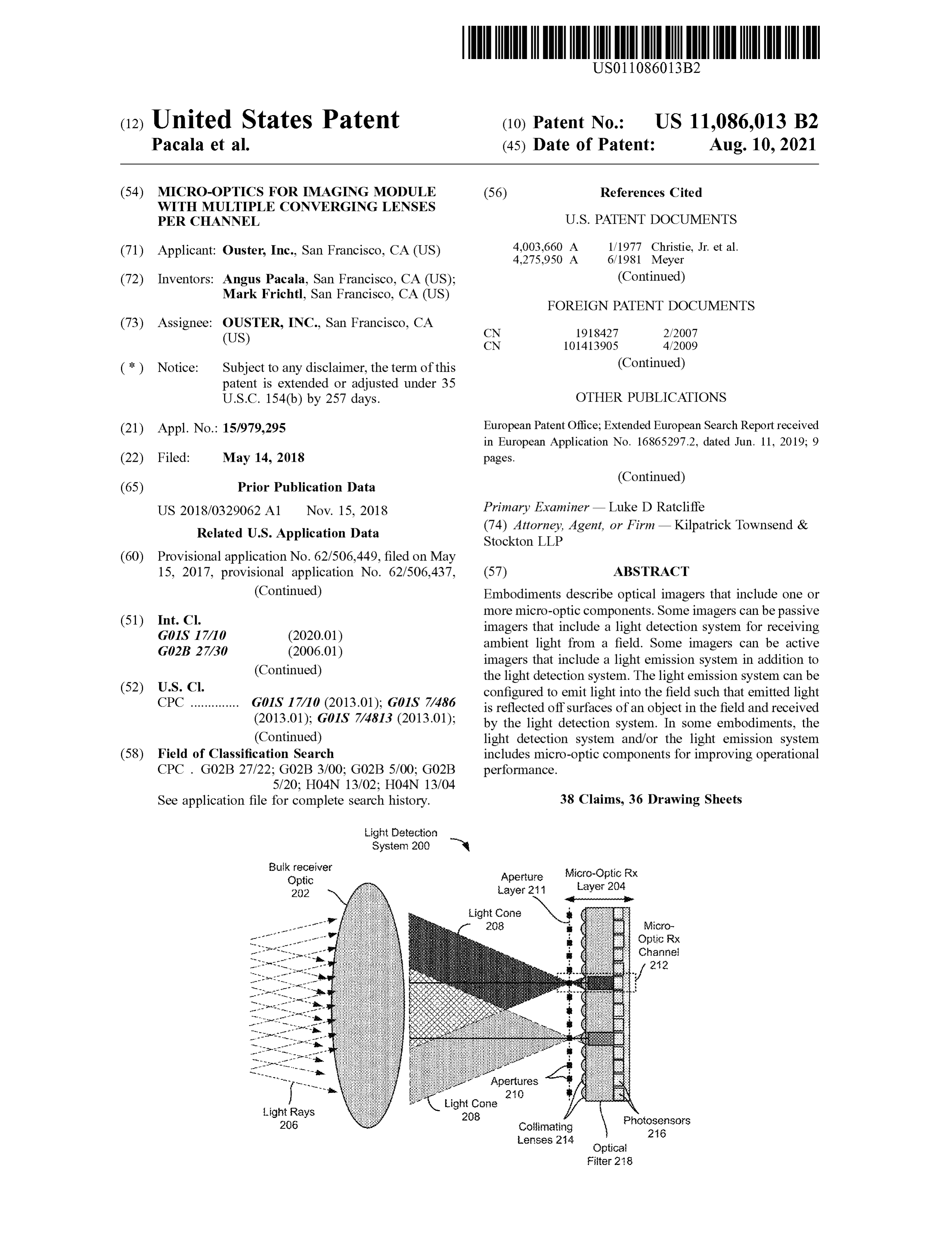
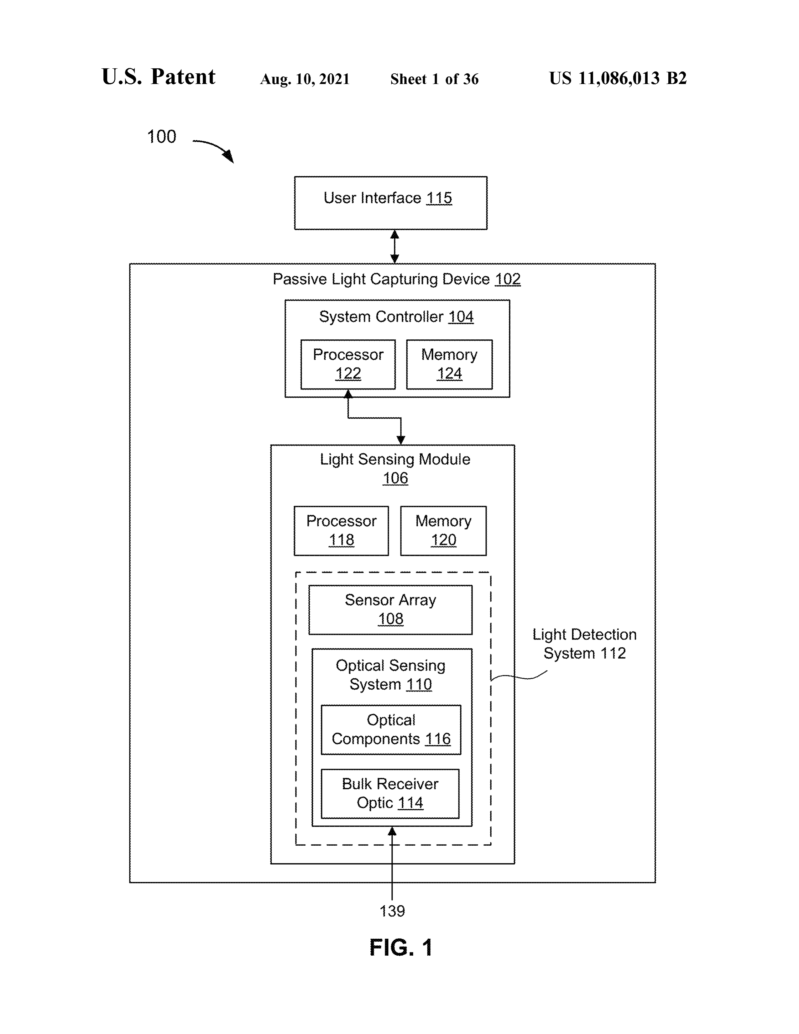
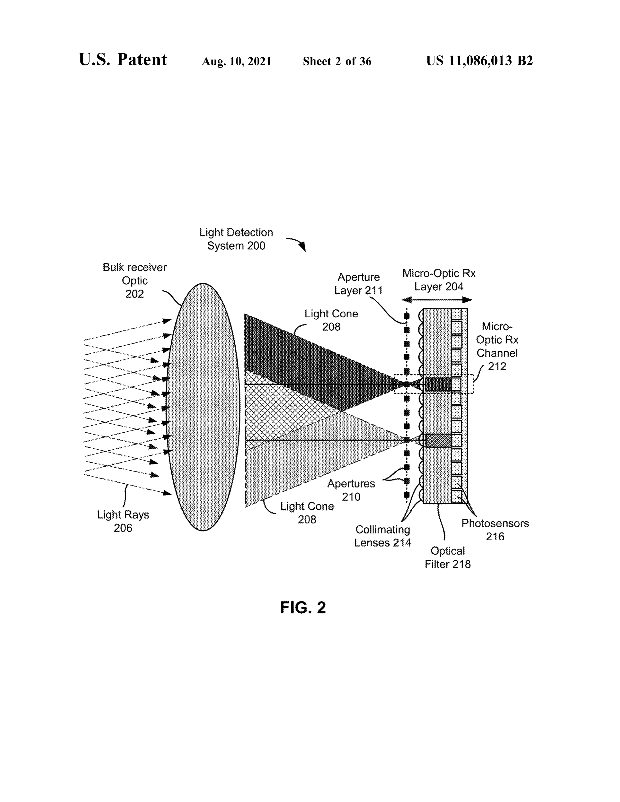
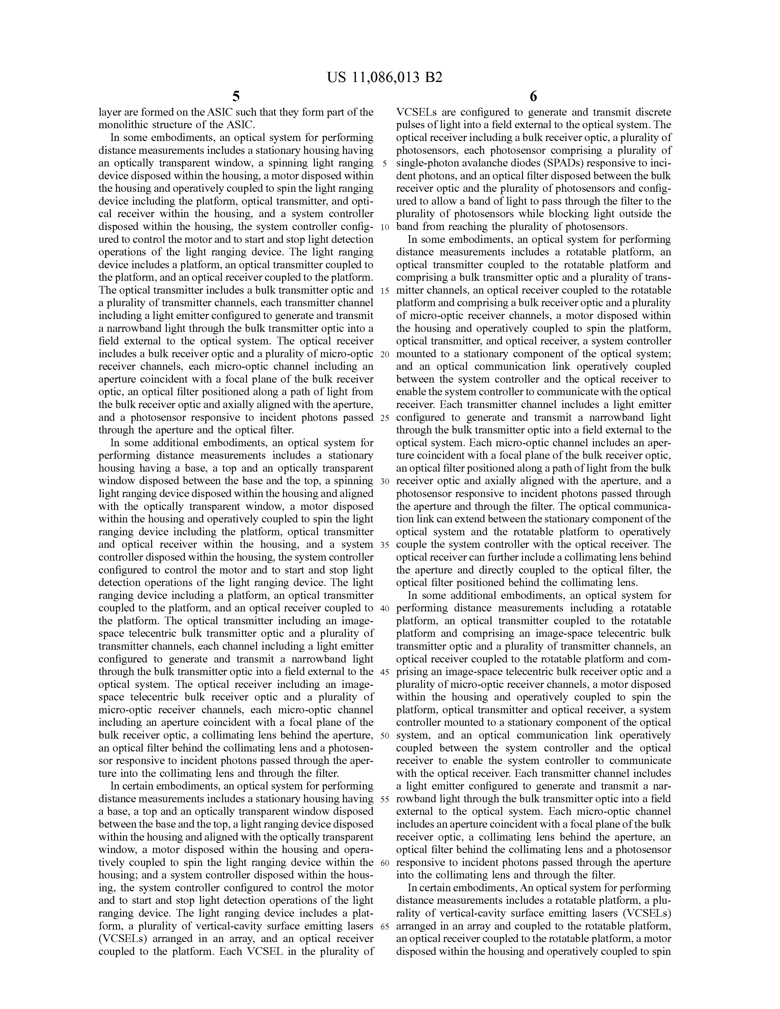
In some additional embodiments, an optical system for BRIEF DESCRIPTION OF THE DRAWINGS performing distance measurements includes a light emission system and a light detection system . The light emission 40 FIG . 1 is a block diagram of an exemplary passive optical system including a bulk transmitter optic and an illumination imager system , according to some embodiments of the source . The illumination source including a plurality of light present disclosure.
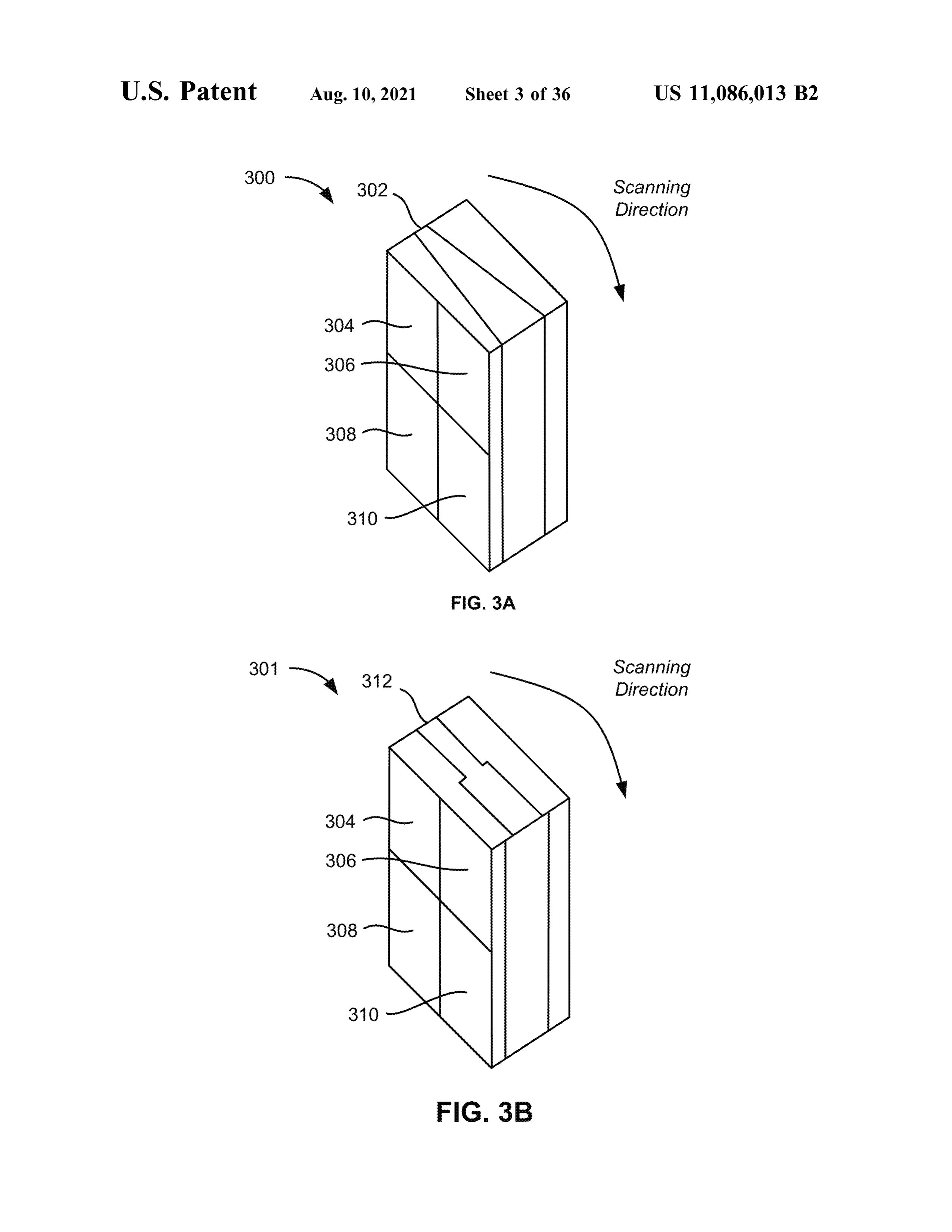
emitters aligned to project discrete beams of light through FIG . 2 is a simplified diagram of an exemplary light the bulk transmitter optic into a field ahead of the optical detection system for a passive optical imager system , system . The light detection system including a bulk receiver 45 according to some embodiments of the present disclosure . optic , an aperture layer including a plurality of apertures, a FIGS . 3A and 3B are perspective views of a simplified first lens layer including a first plurality of lenses , an optical diagram of different embodiments of micro - optic receiver filter layer configured to receive light after it passes through layers with graduated filter layers, according to some the bulk receiver optic and pass a band of radiation while embodiments of the present disclosure.
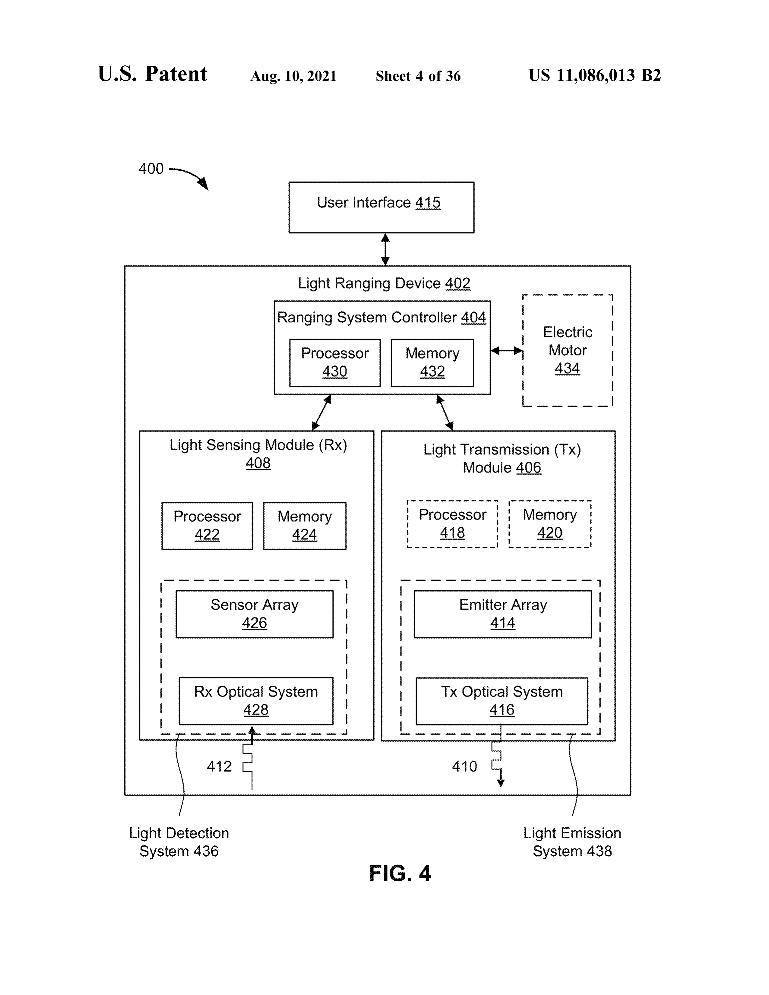
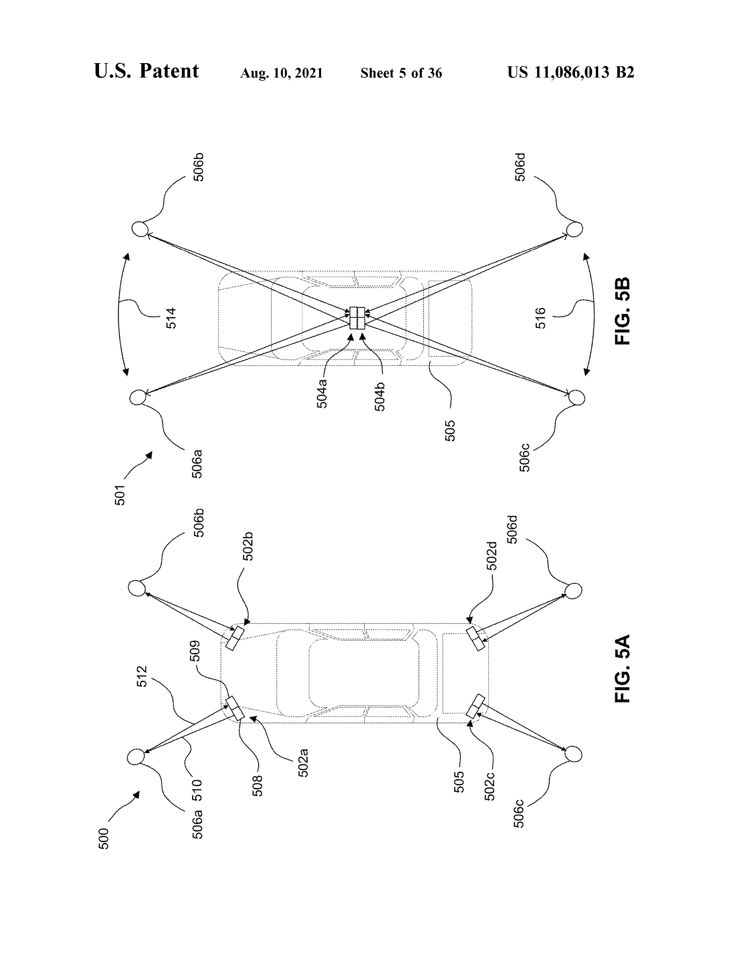
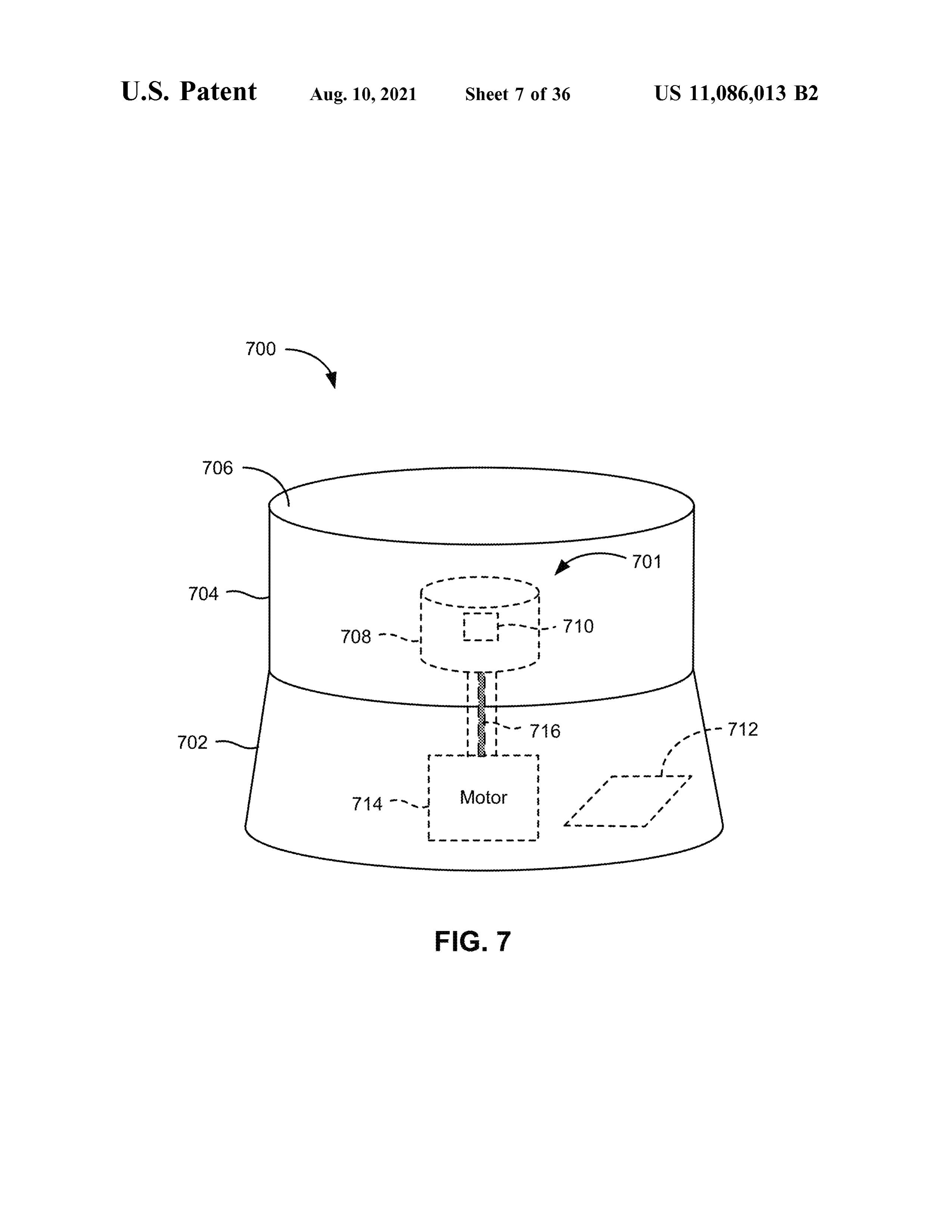
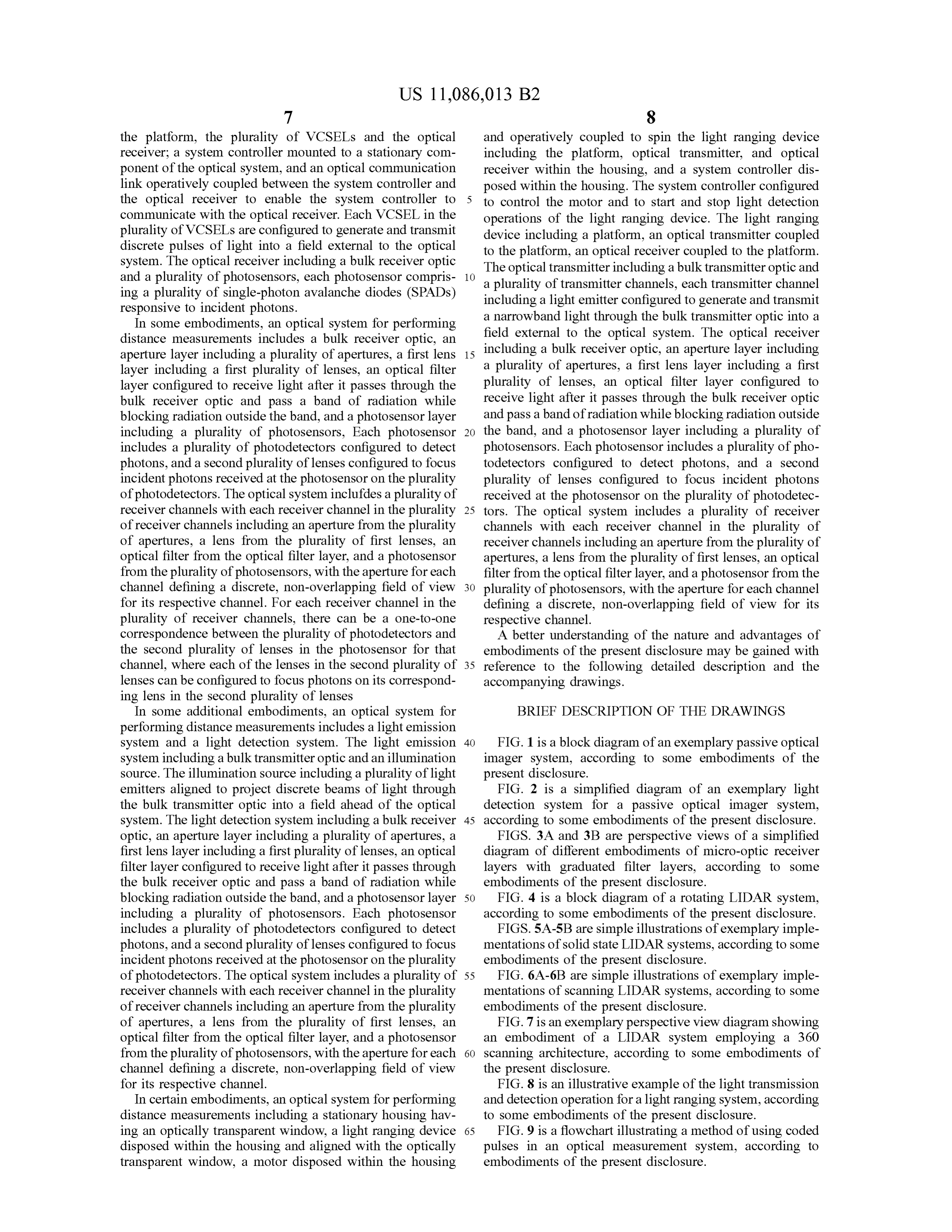
blocking radiation outside the band , and a photosensor layer 50 FIG . 4 is a block diagram of a rotating LIDAR system , including a plurality of photosensors. Each photosensor according to some embodiments of the present disclosure . includes a plurality of photodetectors configured to detect FIGS . 5A - 5B are simple illustrations of exemplary imple photons , and a second plurality of lenses configured to focus mentations of solid state LIDAR systems , according to some incident photons received at the photosensor on the plurality embodiments of the present disclosure . of photodetectors. The optical system includes a plurality of 55 FIG . 6A - 6B are simple illustrations of exemplary imple receiver channels with each receiver channel in the plurality mentations of scanning LIDAR systems , according to some of receiver channels including an aperture from the plurality embodiments of the present disclosure . of apertures, a lens from the plurality of first lenses , an FIG . 7 is an exemplary perspective view diagram showing optical filter from the optical filter layer, and a photosensor an embodiment of a LIDAR system employing a 360 from the plurality of photosensors , with the aperture for each 60 scanning architecture , according to some embodiments of channel defining a discrete , non - overlapping field of view the present disclosure.
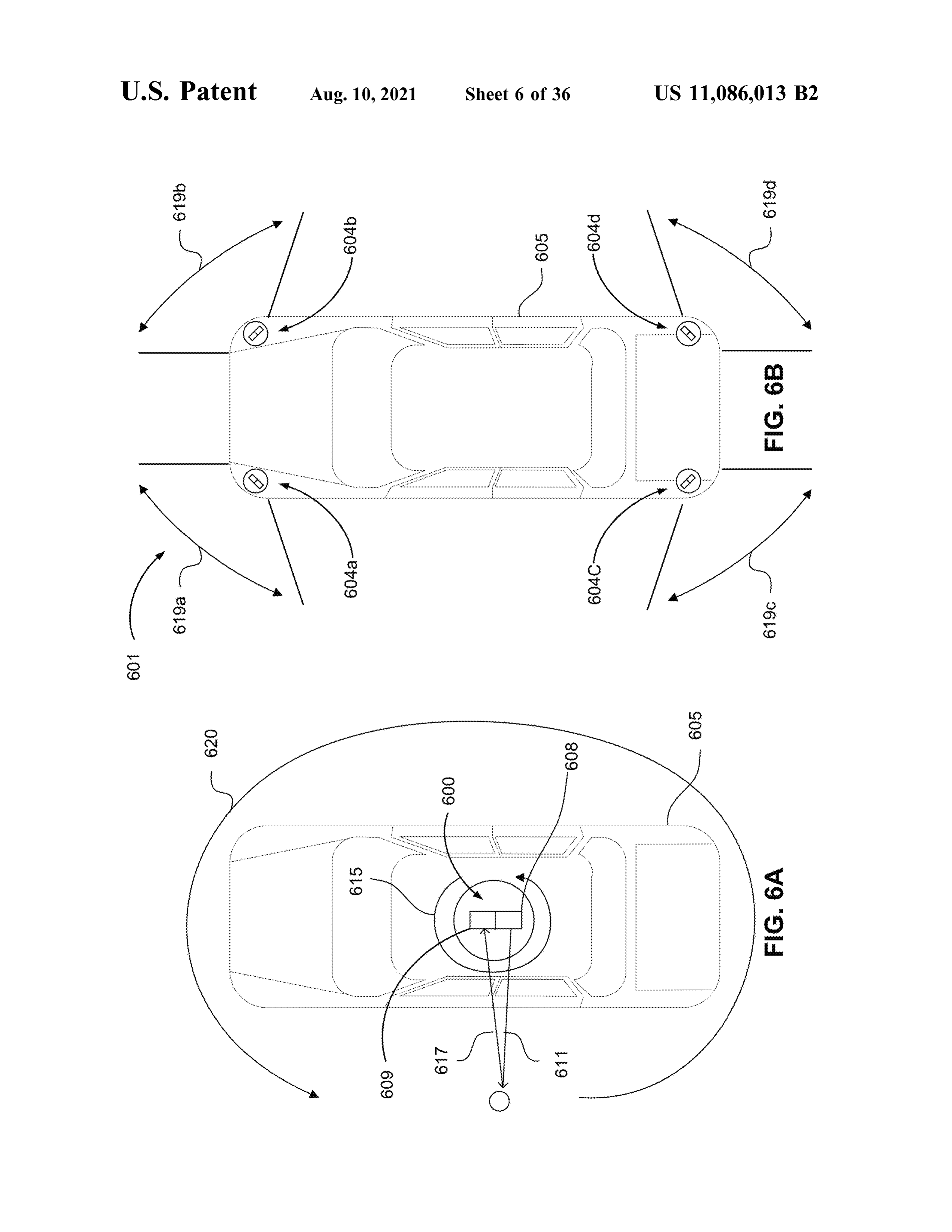
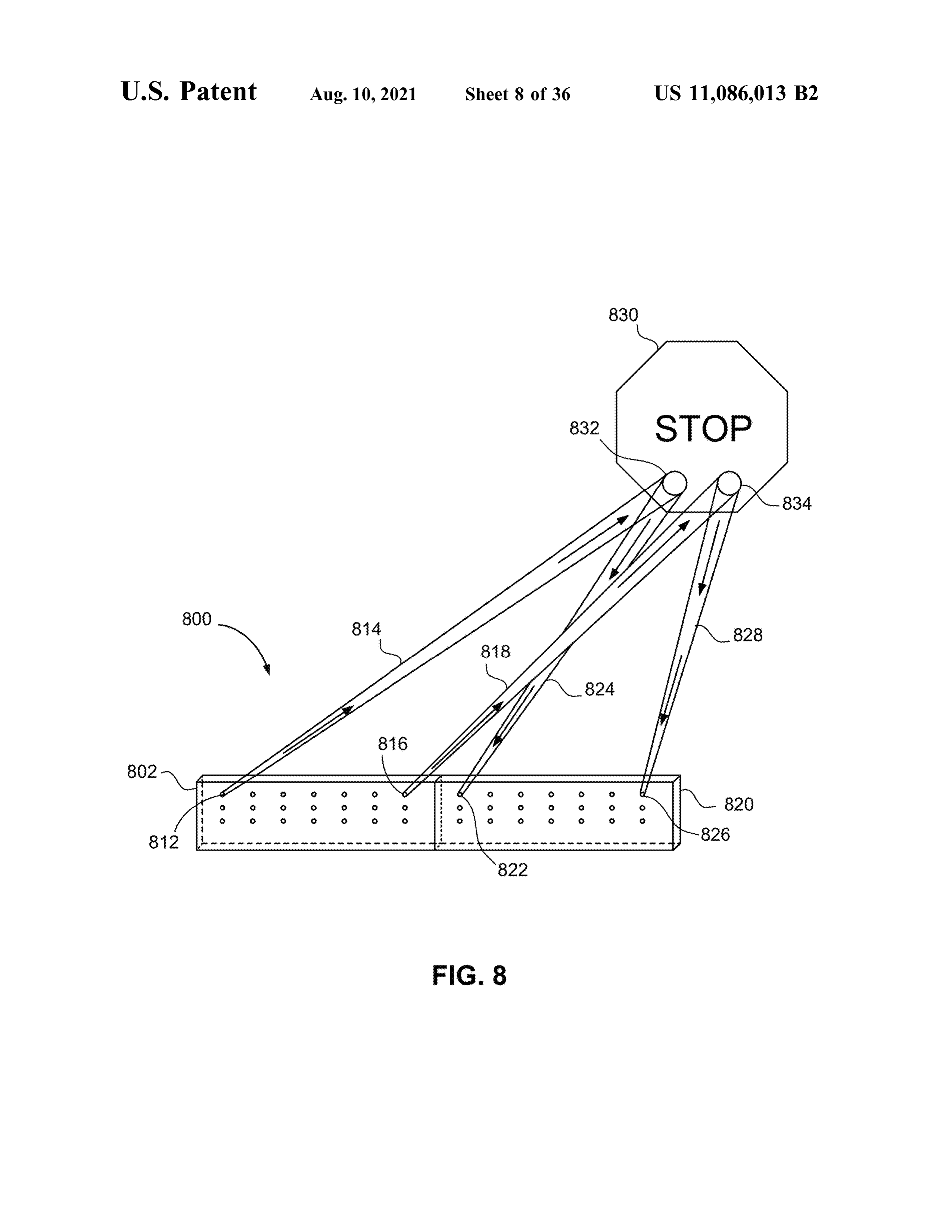
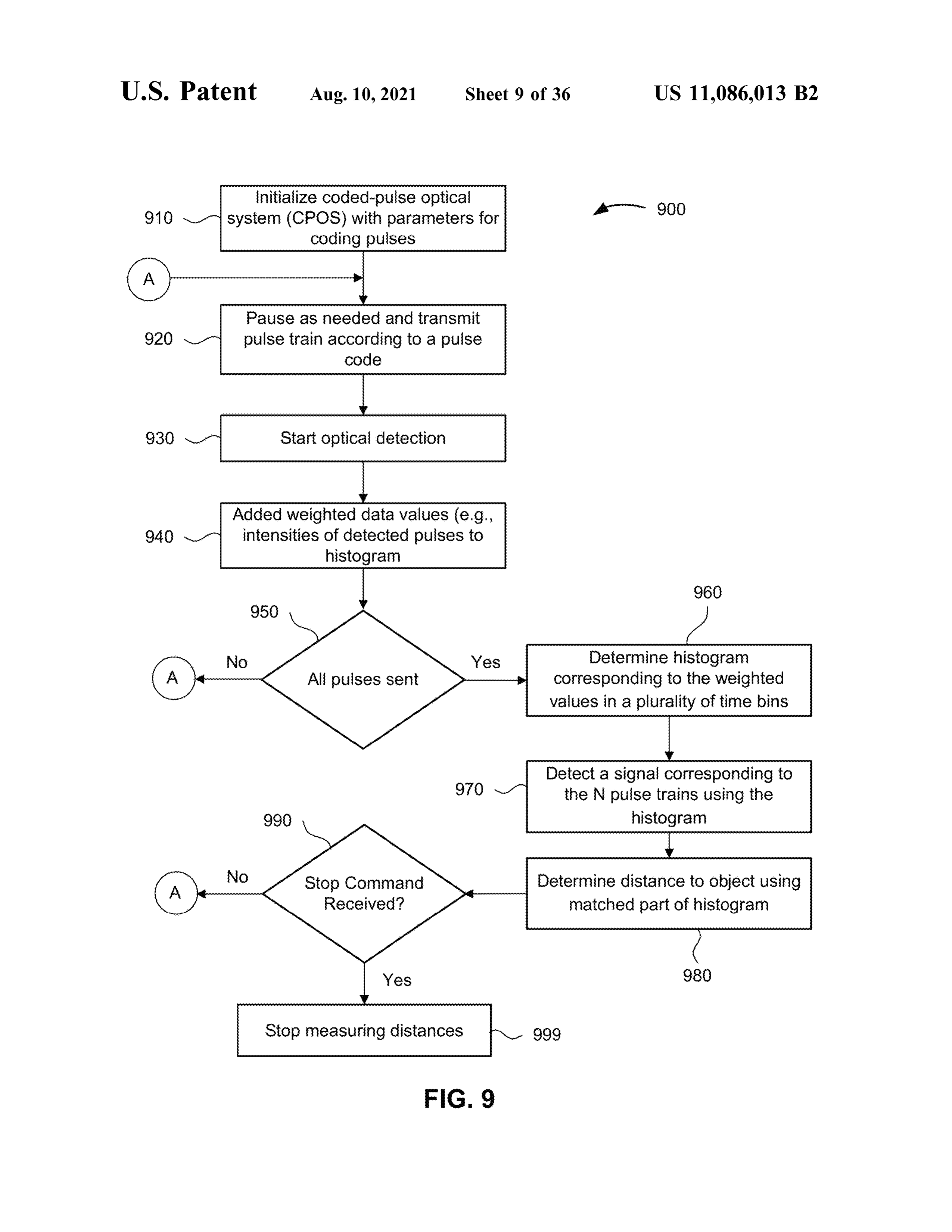
for its respective channel. FIG . 8 is an illustrative example of the light transmission In certain embodiments, an optical system for performing and detection operation for a light ranging system , according distance measurements including a stationary housing hav- to some embodiments of the present disclosure . ing an optically transparent window , a light ranging device 65 FIG . 9 is a flowchart illustrating a method of using coded disposed within the housing and aligned with the optically pulses in an optical measurement system , according to transparent window, a motor disposed within the housing embodiments of the present disclosure .
Page 45
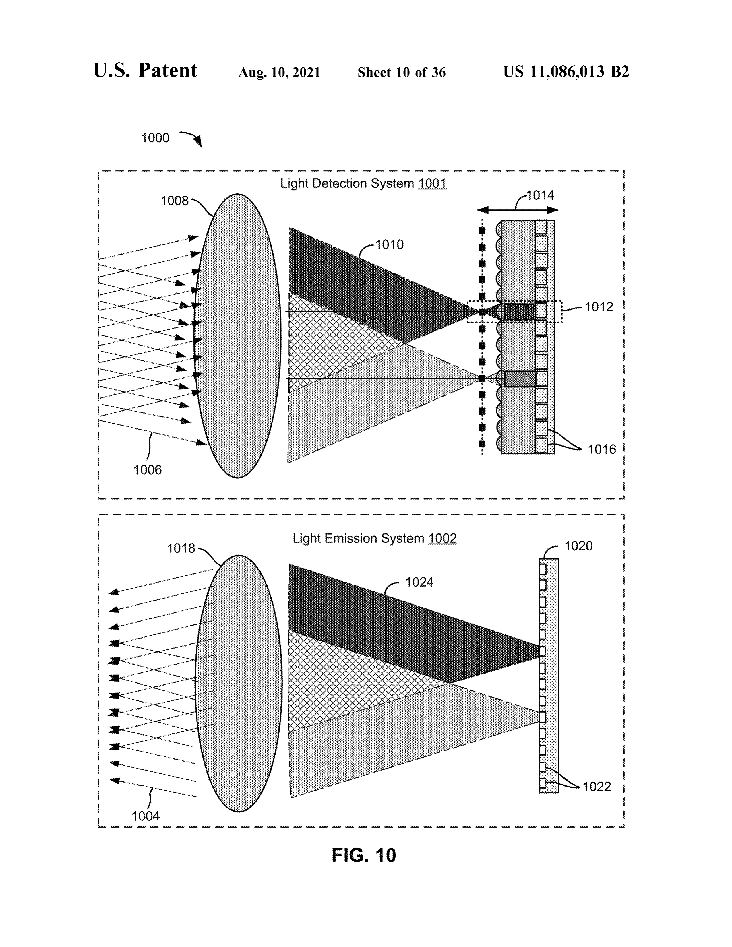
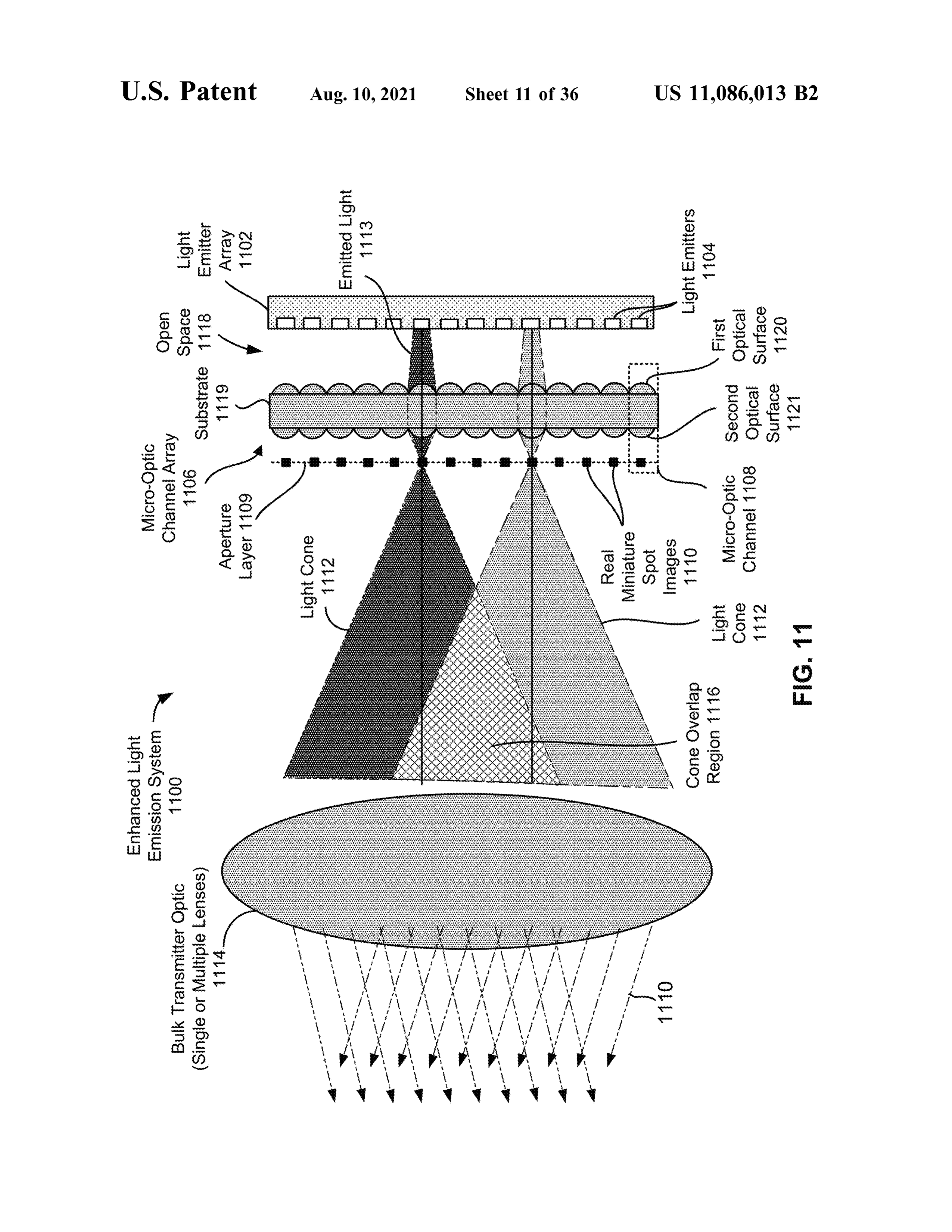
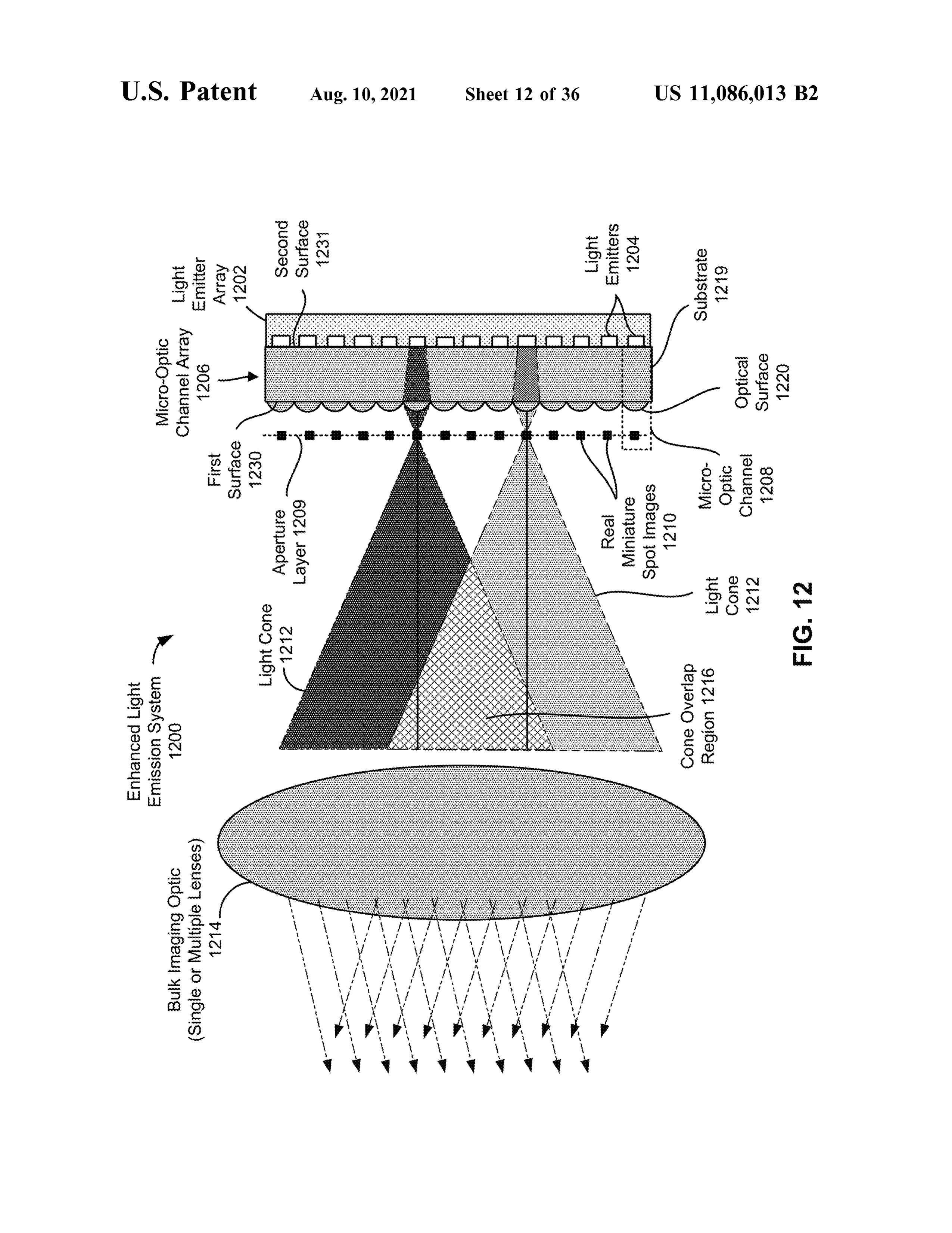
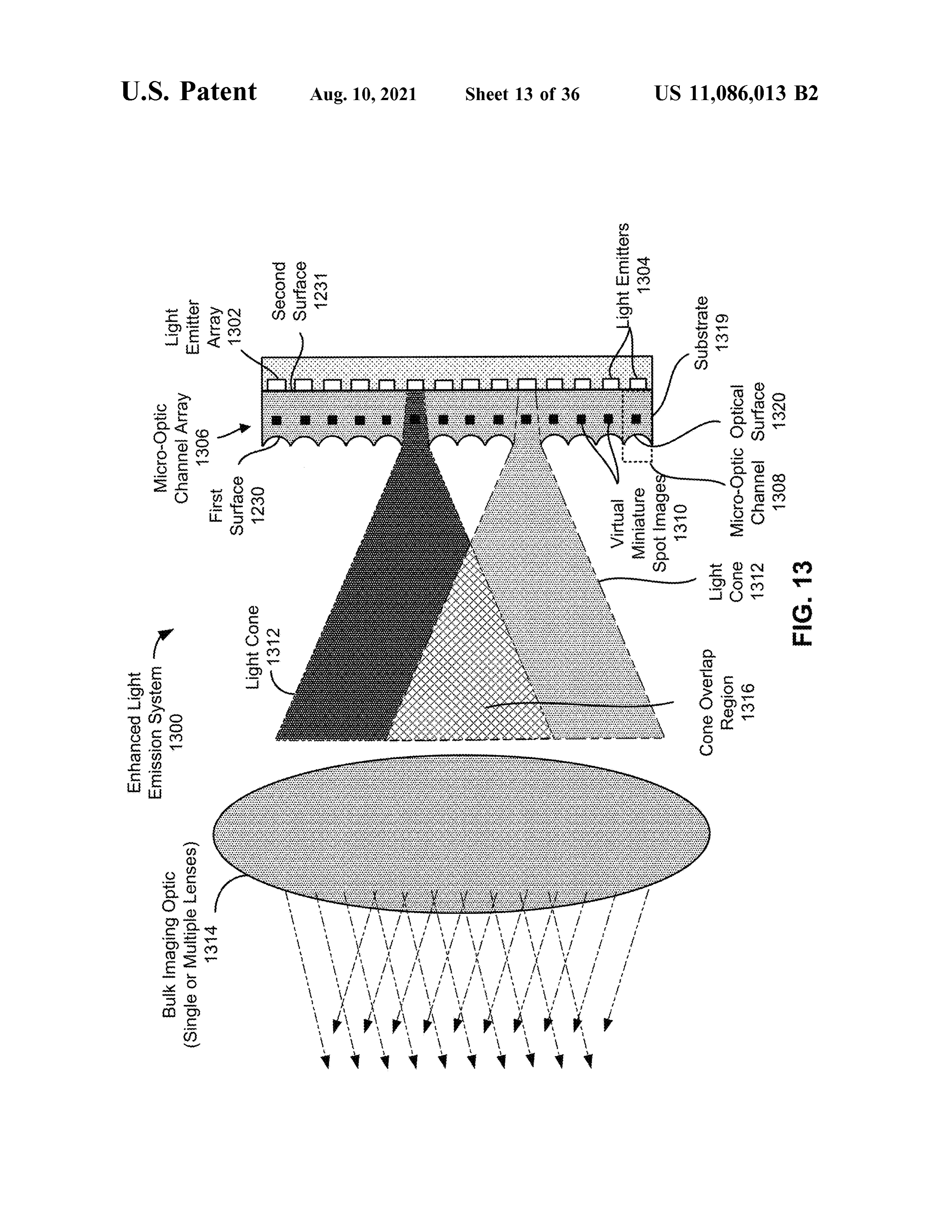
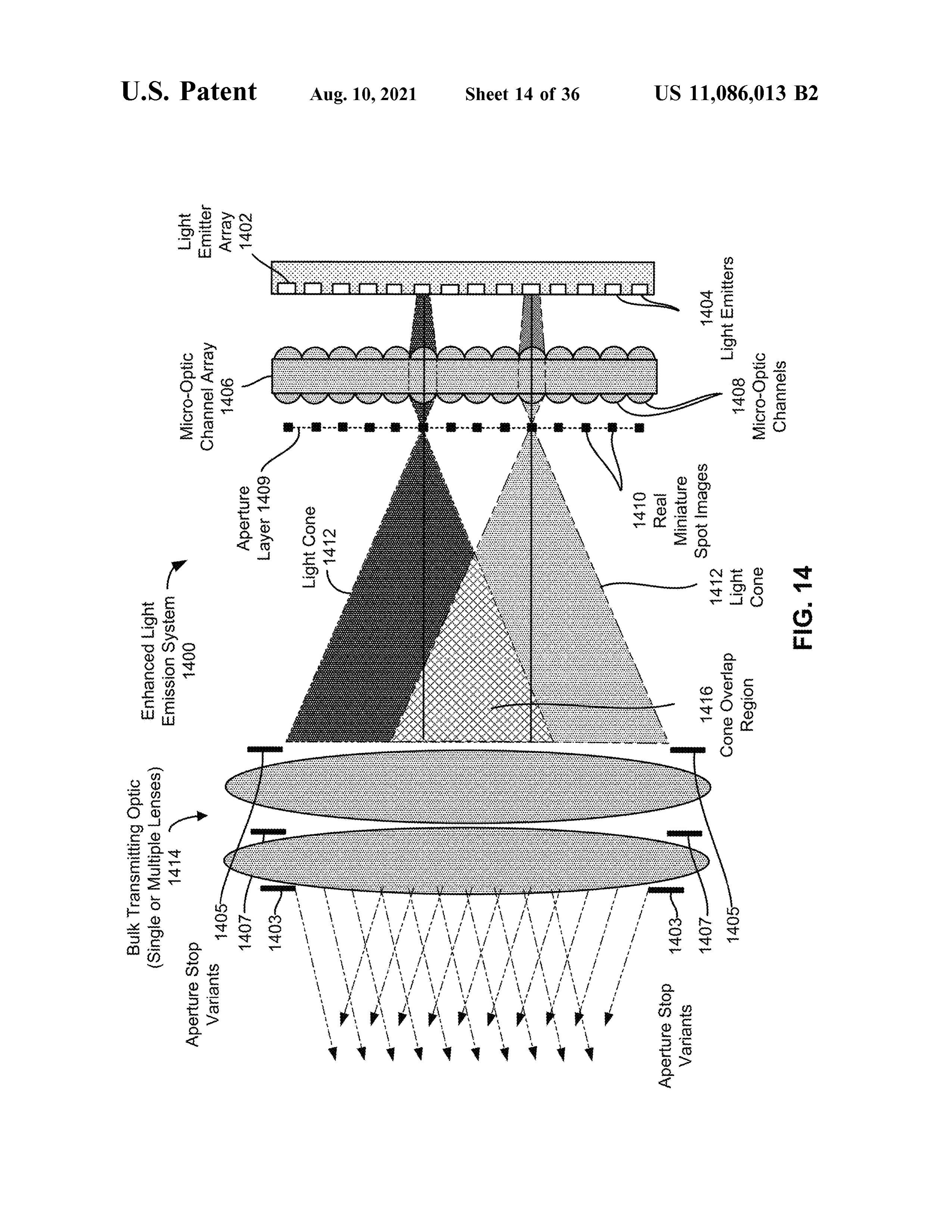
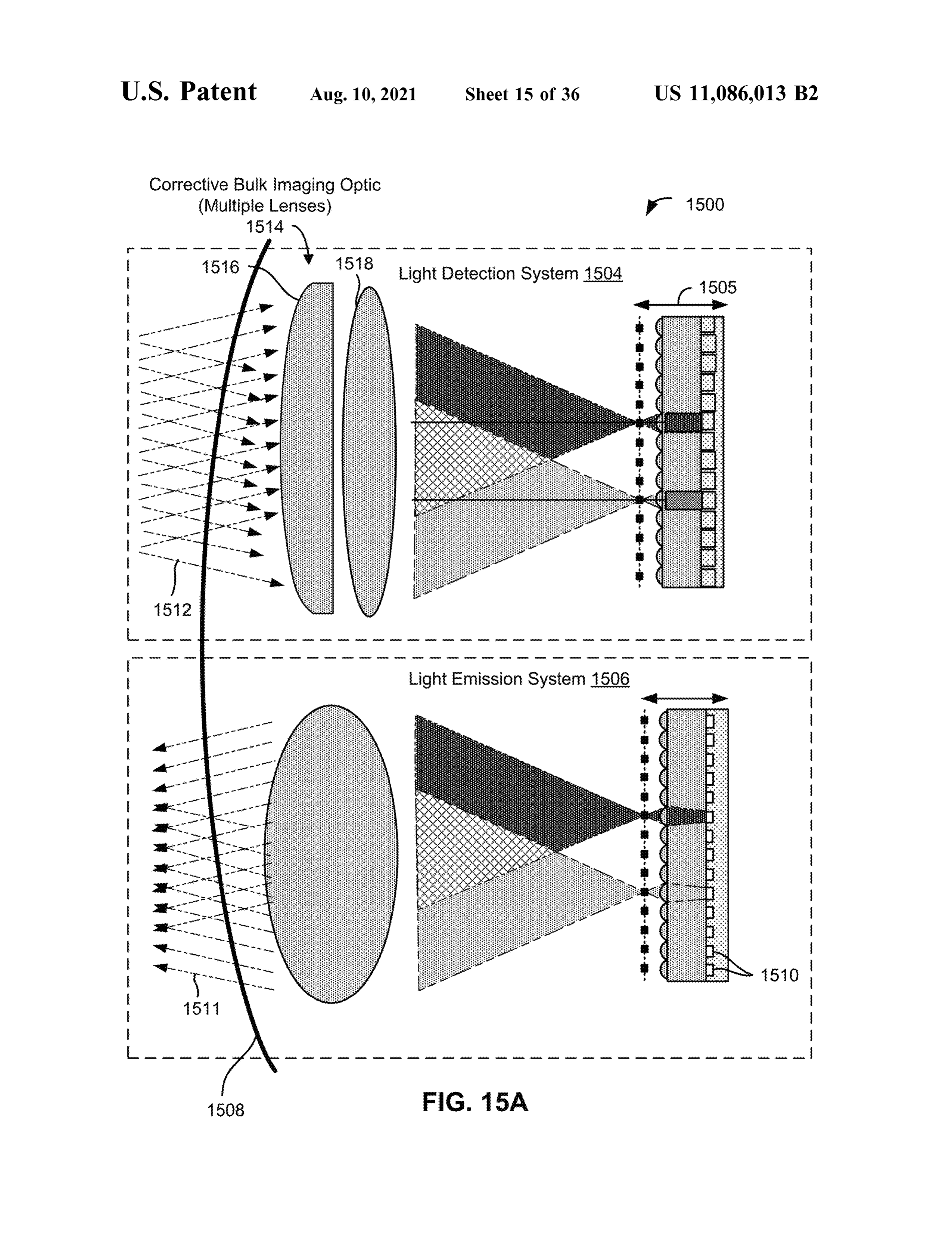
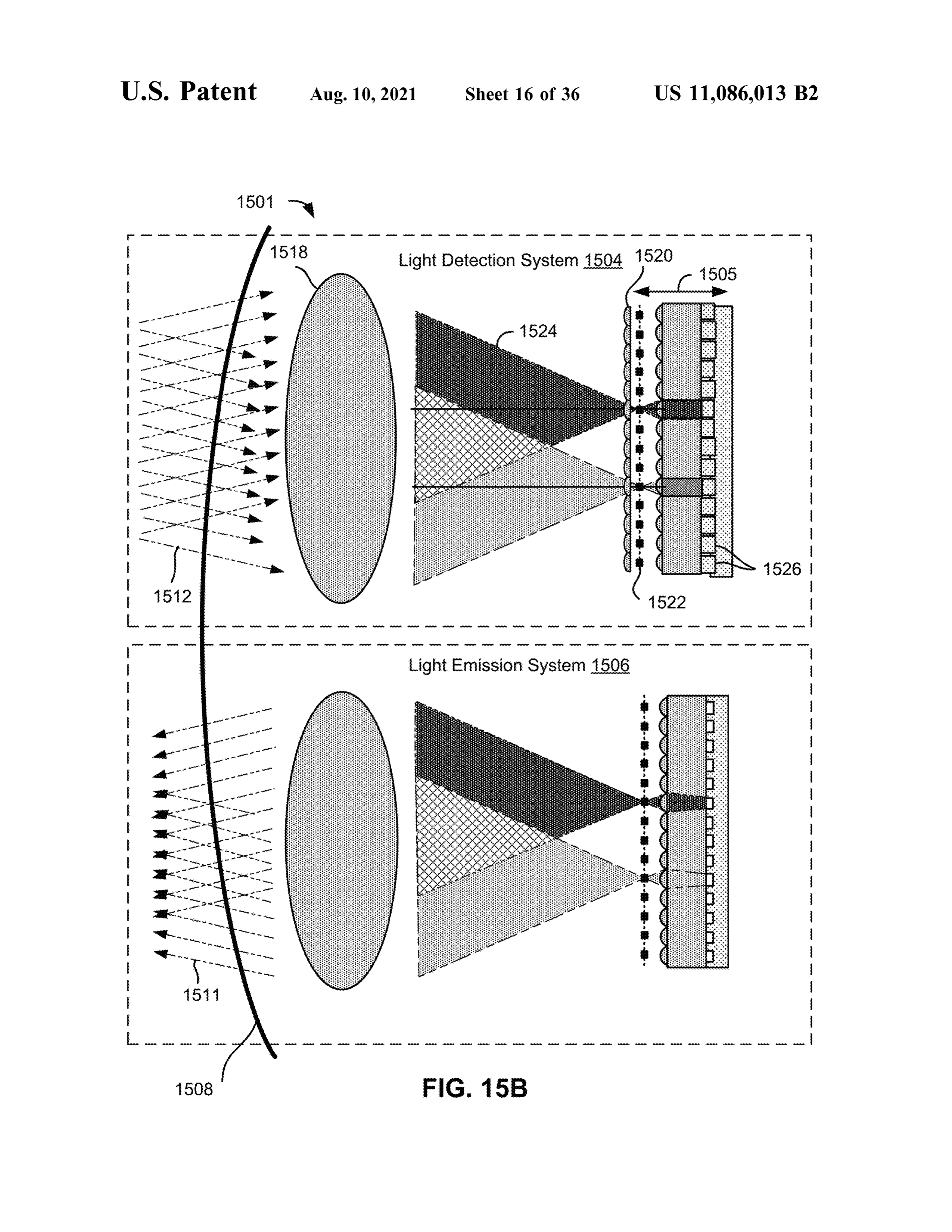
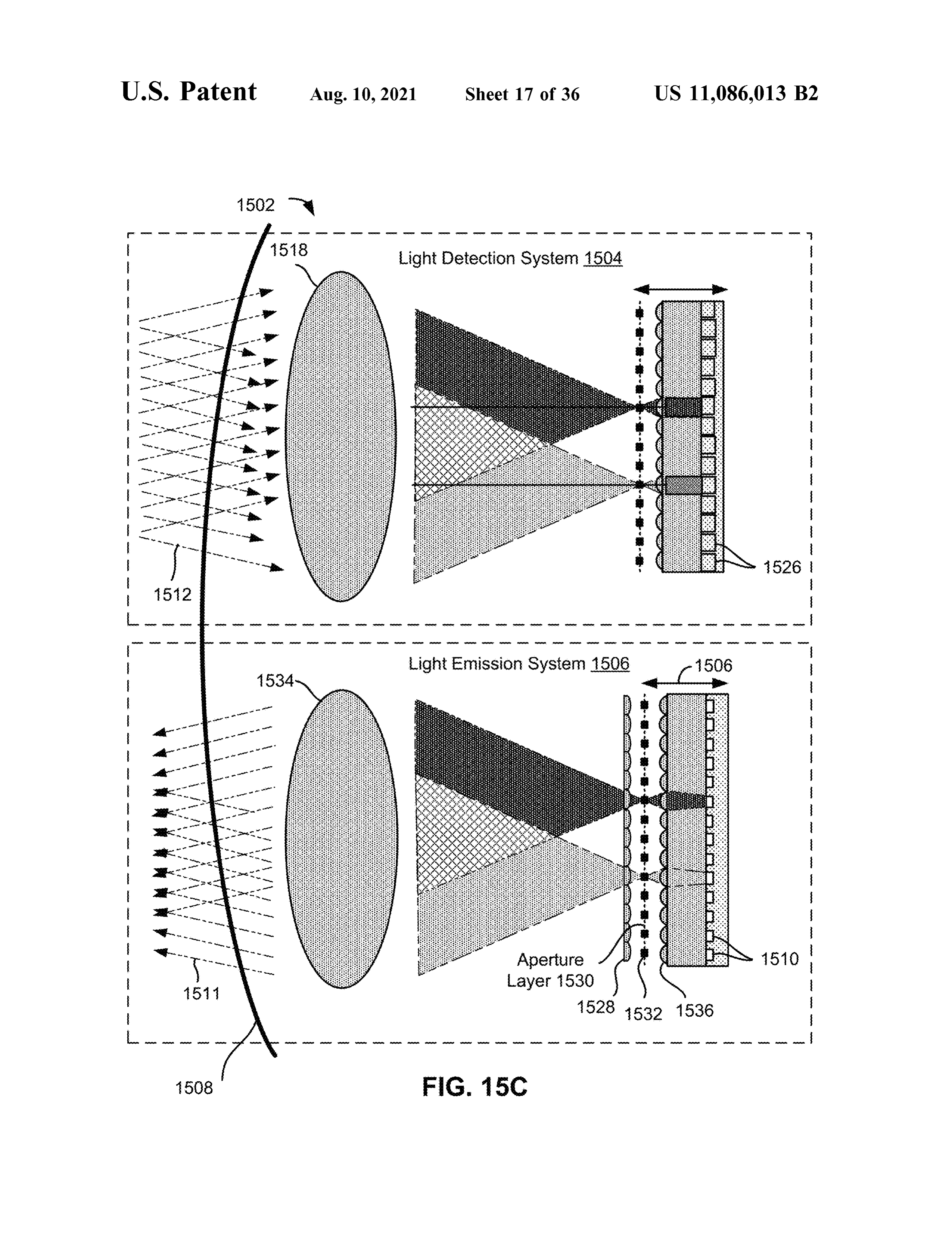
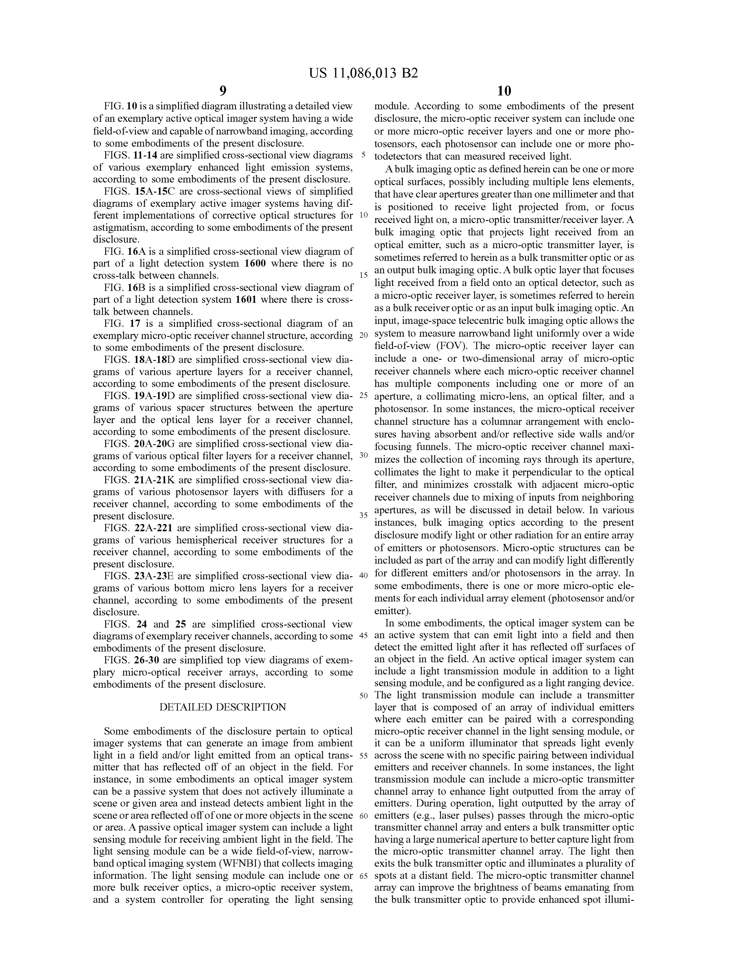
FIG . 10 is a simplified diagram illustrating a detailed view module. According to some embodiments of the present of an exemplary active optical imager system having a wide disclosure, the micro -optic receiver system can include one field - of - view and capable of narrowband imaging , according or more micro - optic receiver layers and one or more pho to some embodiments of the present disclosure . tosensors, each photosensor can include one or more pho FIGS . 11-14 are simplified cross - sectional view diagrams 5 todetectors that can measured received light. of various exemplary enhanced light emission systems, A bulk imaging optic as defined herein can be one or more according to some embodiments of the present disclosure . optical surfaces, possibly including multiple lens elements, FIGS . 15A - 15C are cross - sectional views of simplified diagrams of exemplary active imager systems having dif that have clear apertures greater than one millimeter and that is positioned to receive light projected from , or focus ferent implementations of corrective optical structures for 10 received light on, a micro -optic transmitter / receiver layer. A astigmatism , according to some embodiments of the present bulk imaging optic that projects light received from an disclosure .
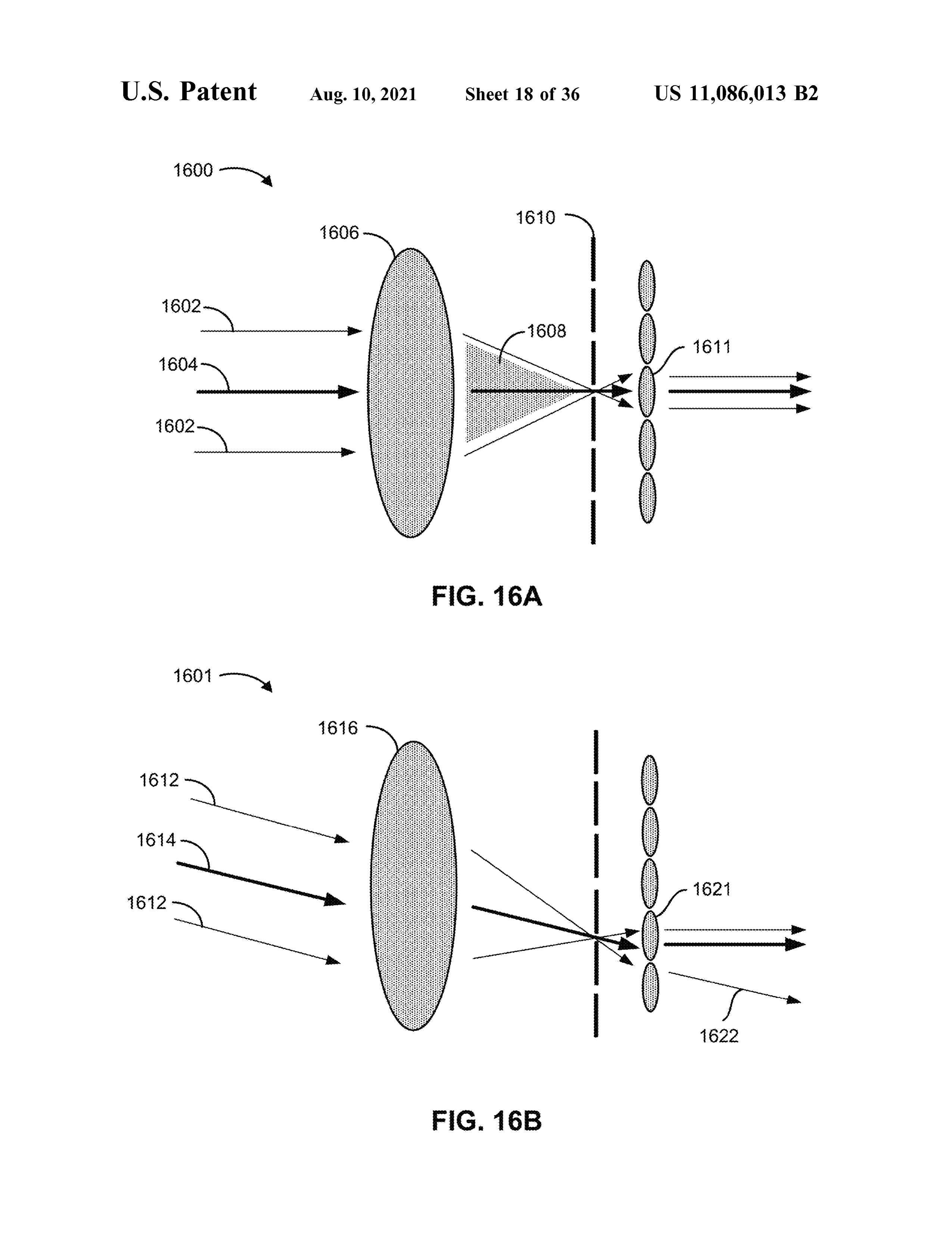
FIG . 16A is a simplified cross - sectional view diagram of optical emitter, such as a micro - optic transmitter layer, is sometimes referred to herein as a bulk transmitter optic or as part of a light detection system 1600 where there is no an output bulk imaging optic . A bulk optic layer that focuses cross -talk between channels . 15
FIG . 16B is a simplified cross - sectional view diagram of alight received from a field onto an optical detector, such as part of a light detection system 1601 where there is cross as a bulk- optic micro receiver layer, is sometimes referred to herein receiver optic or as an input bulk imaging optic . An talk between channels.
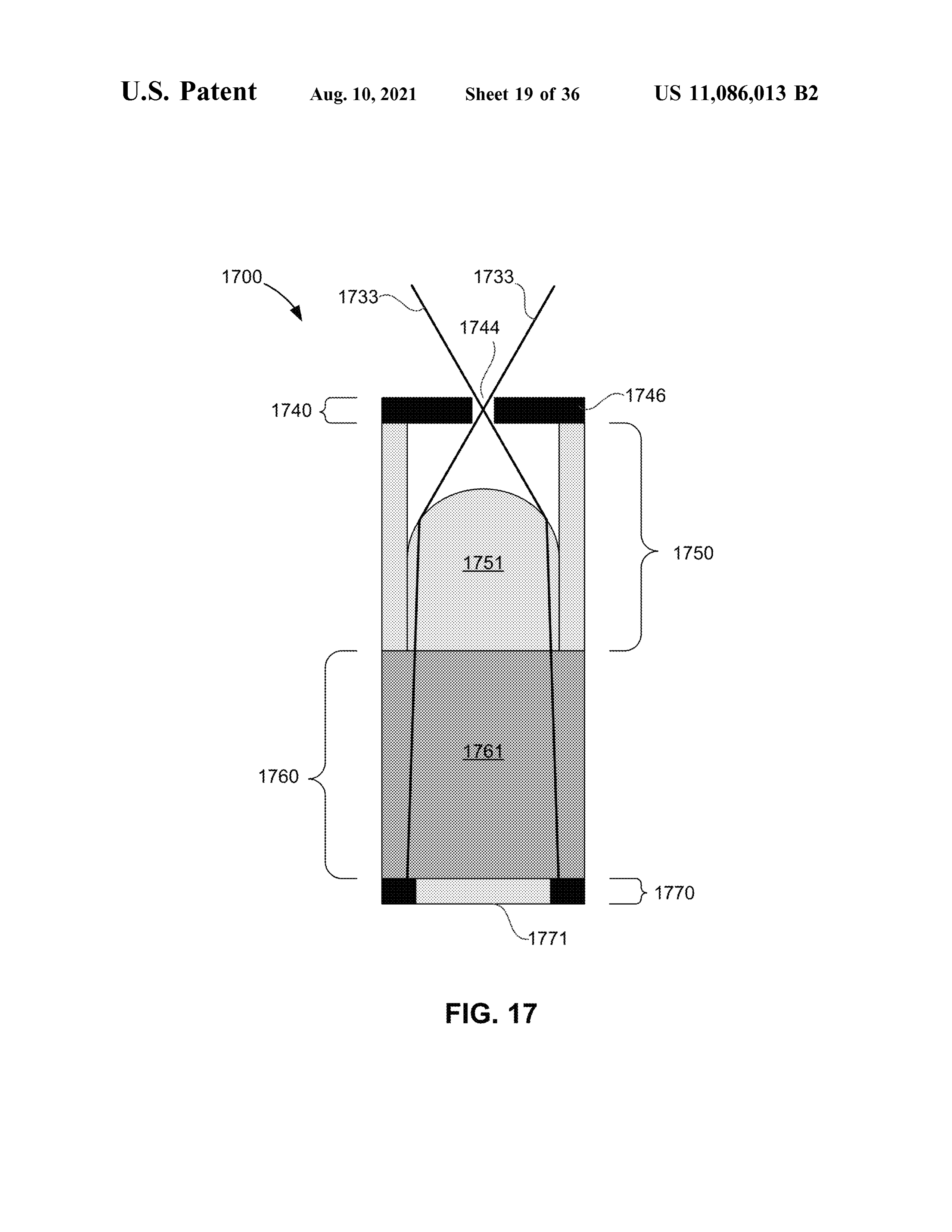
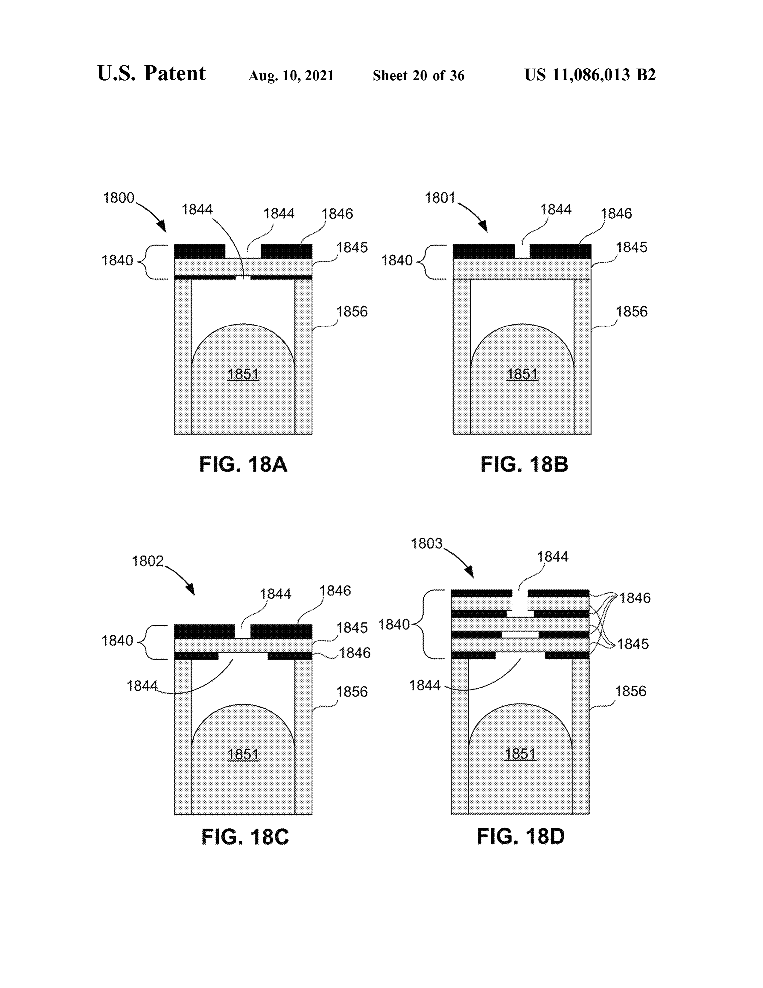
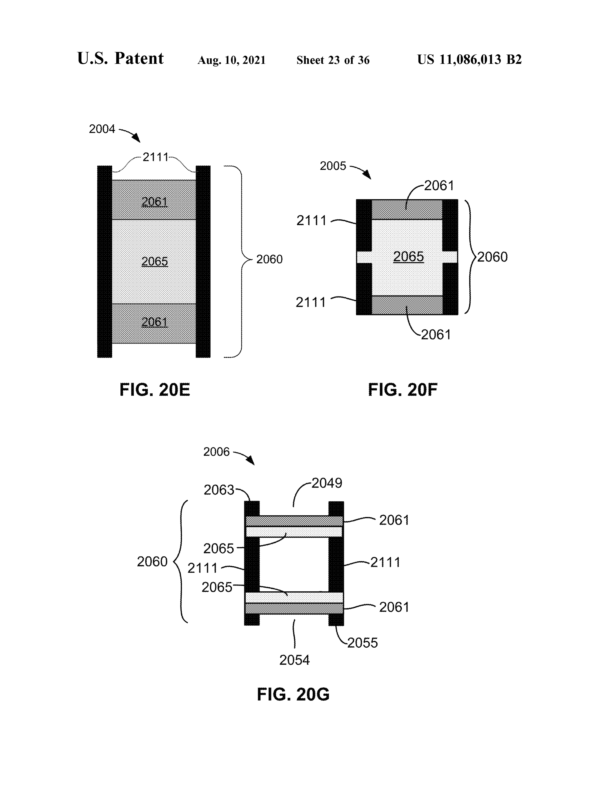
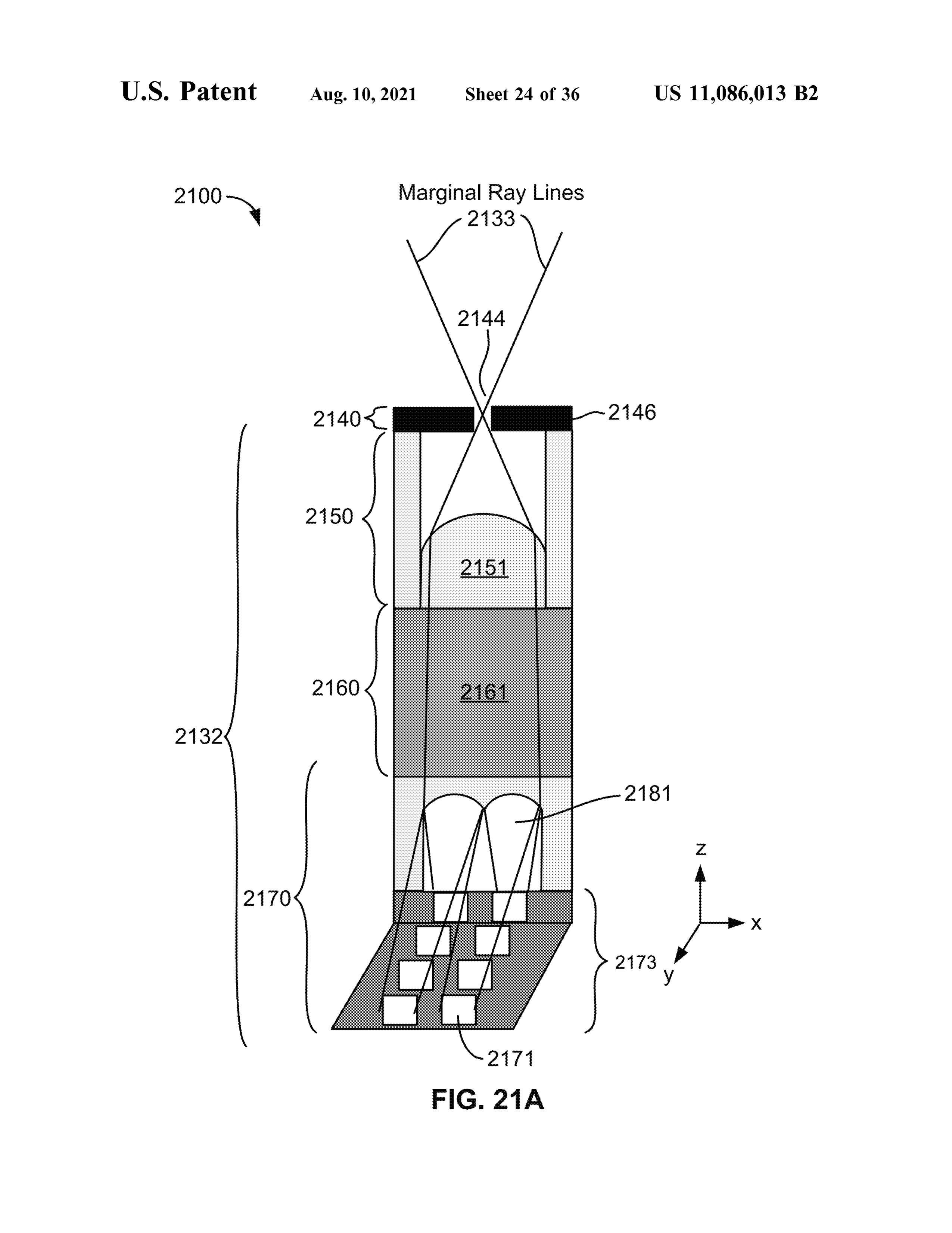
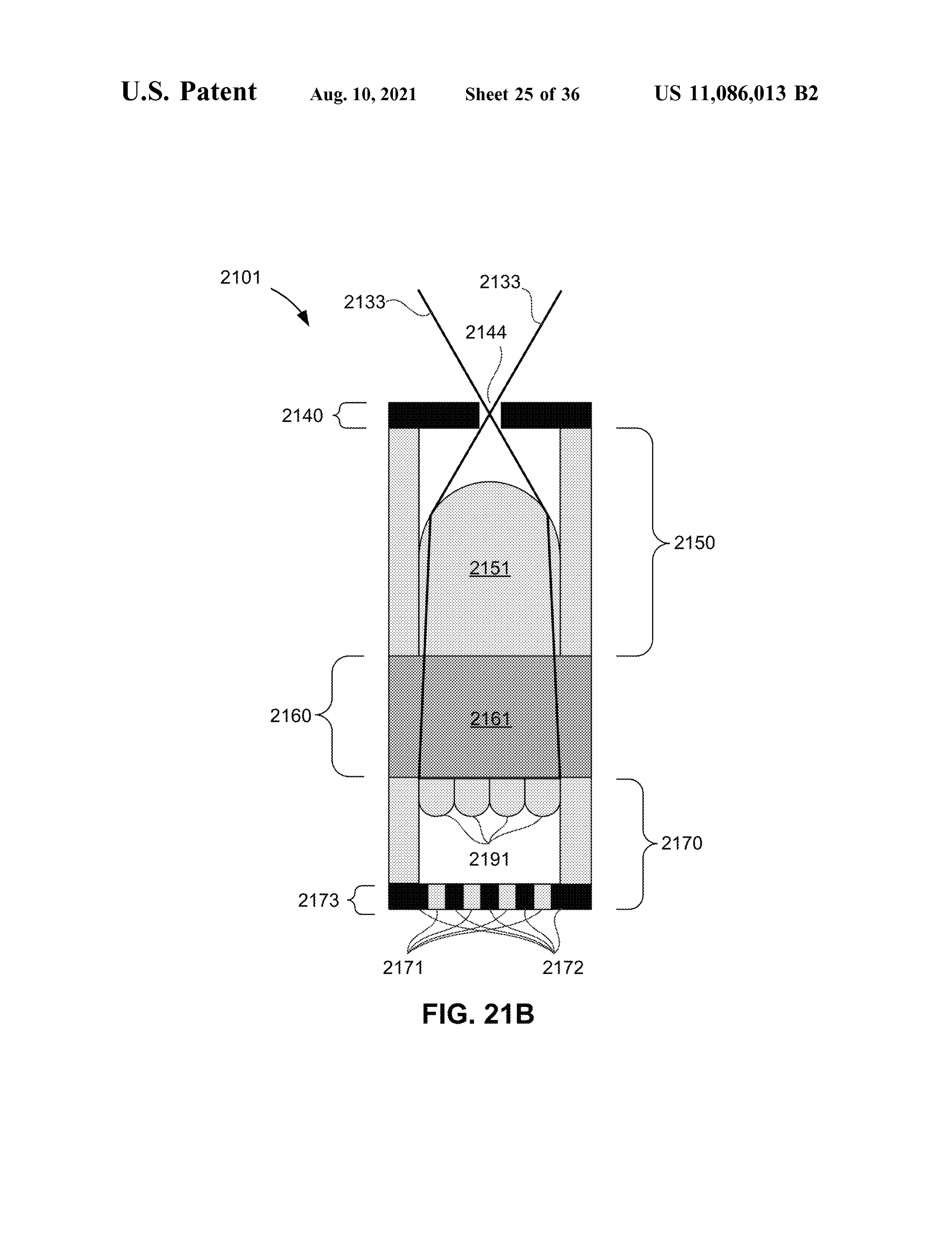
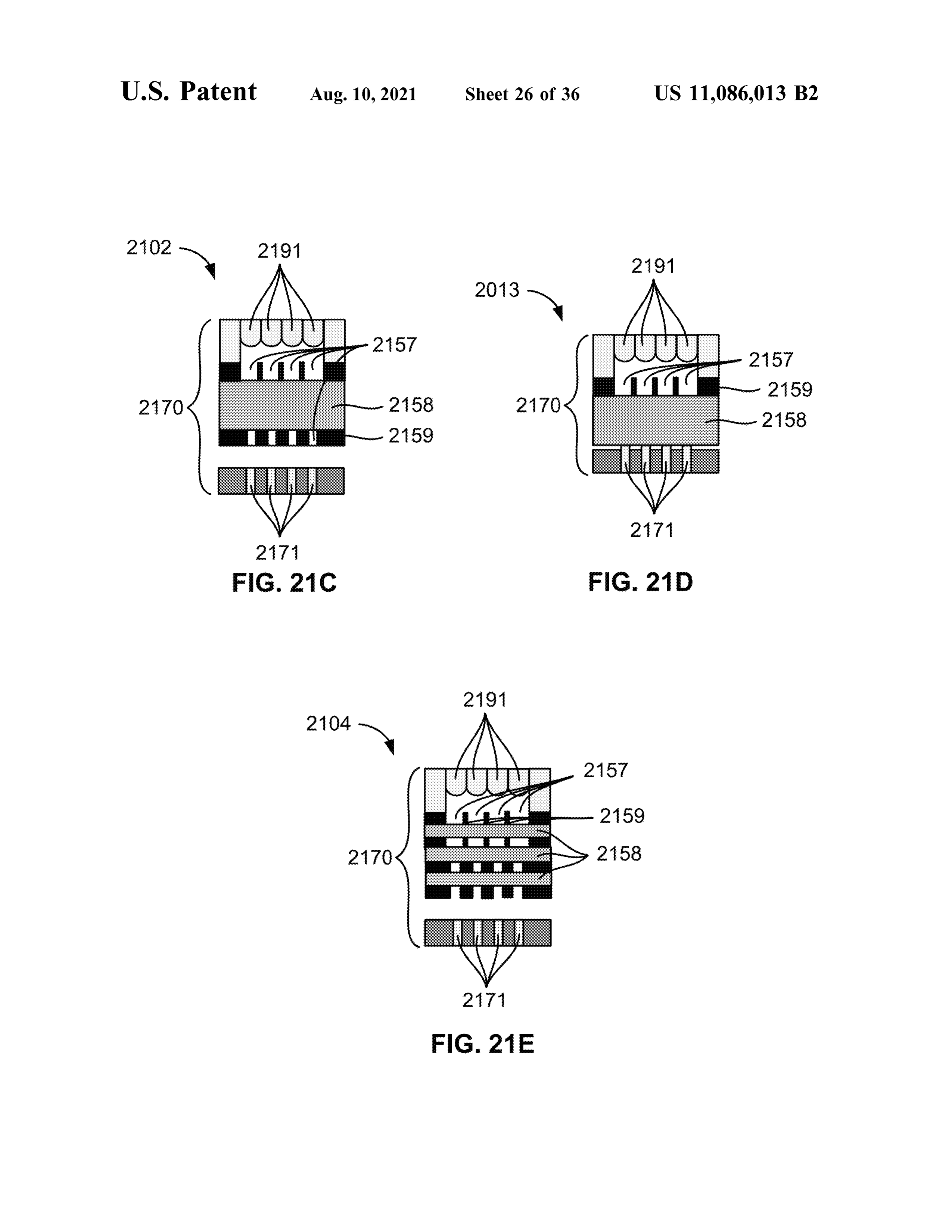
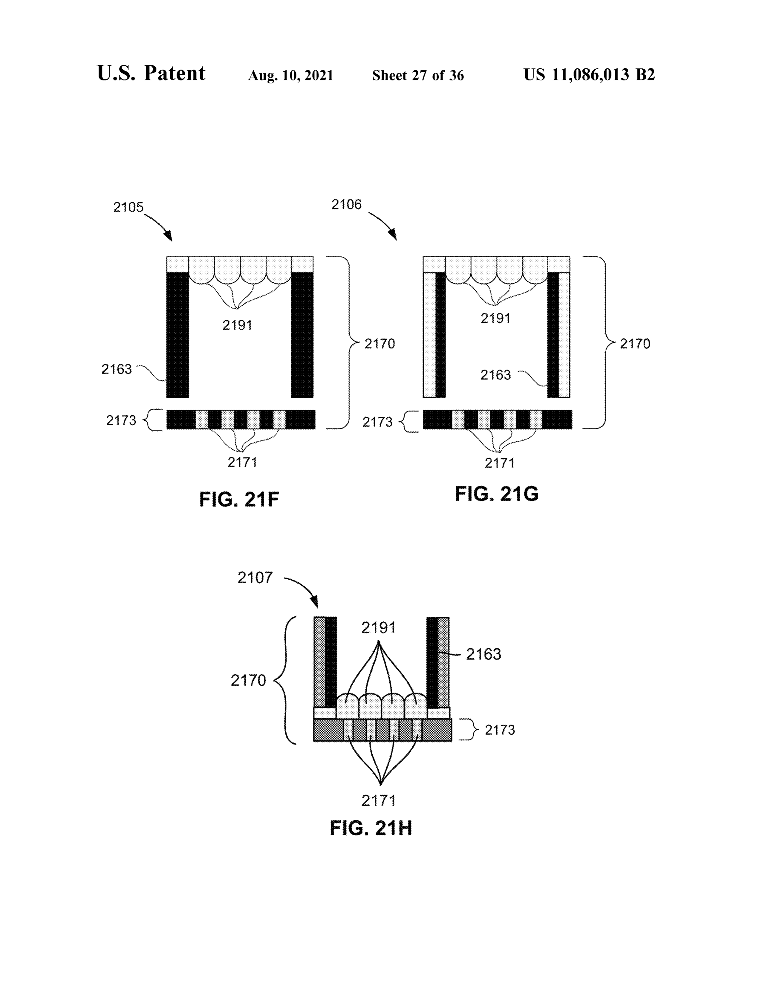
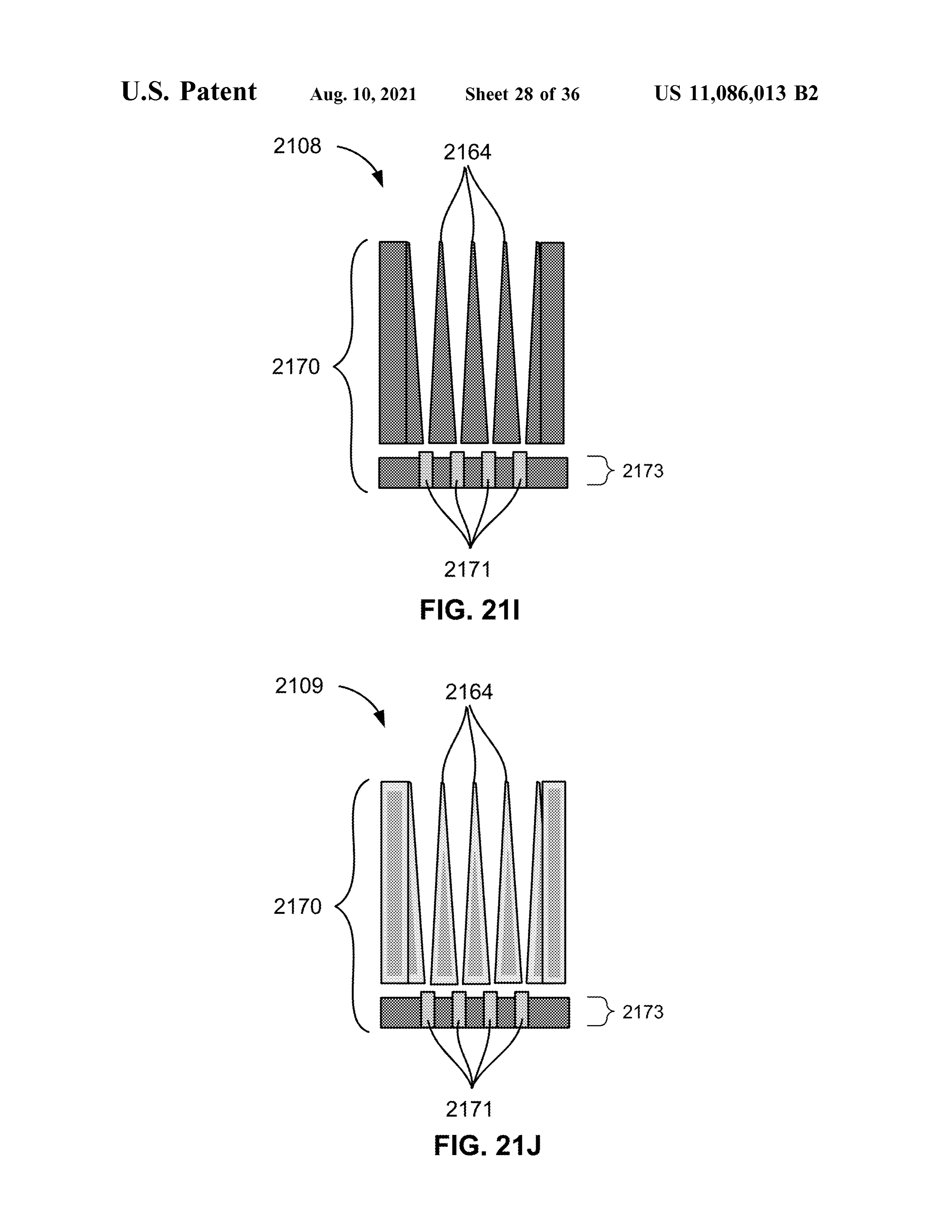
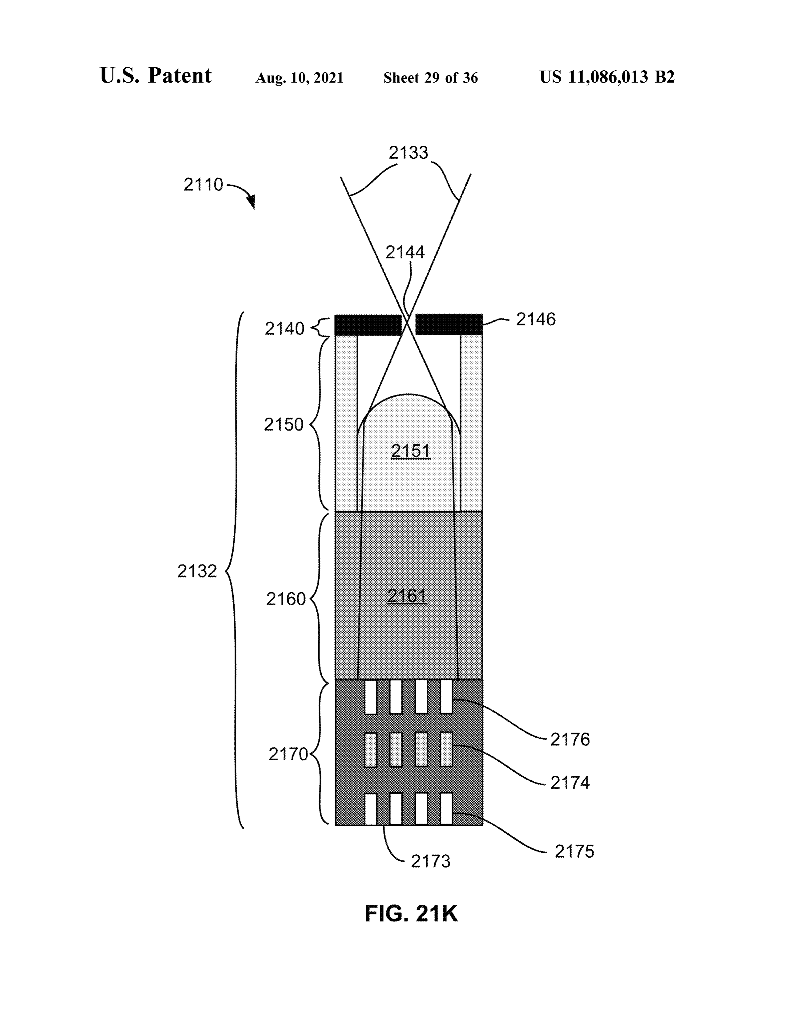
FIG . 17 is a simplified cross - sectional diagram of an input, image - space telecentric bulk imaging optic allows the exemplary micro - optic receiver channel structure , according 20 system to measure narrowband light uniformly over a wide to some embodiments of the present disclosure . field -of -view ( FOV) . The micro - optic receiver layer can FIGS . 18A - 18D are simplified cross - sectional view dia- include a one- or two - dimensional array of micro -optic grams of various aperture layers for a receiver channel, receiver channels where each micro -optic receiver channel according to some embodiments of the present disclosure . has multiple components including one or more of an FIGS . 19A- 19D are simplified cross-sectional view dia- 25 aperture, a collimating micro -lens , an optical filter, and a grams of various spacer structures between the aperture photosensor. In some instances, the micro -optical receiver layer and the optical lens layer for a receiver channel, channel structure has a columnar arrangement with enclo according to some embodiments of the present disclosure . sures having absorbent and / or reflective side walls and / or FIGS . 20A - 20G are simplified cross - sectional view dia focusing funnels. The micro -optic receiver channel maxi grams of various optical filter layers for a receiver channel, 30 mizes the collection of incoming rays through its aperture, according to some embodiments of the present disclosure . collimates the light to make it perpendicular to the optical FIGS . 21A - 21K are simplified cross - sectional view dia filter, and minimizes crosstalk with adjacent micro -optic grams of various photosensor layers with diffusers for a receiver receiver channel, according to some embodiments of the 35 apertureschannels , as will due to mixing of inputs from neighboring be discussed in detail below. In various present disclosure.
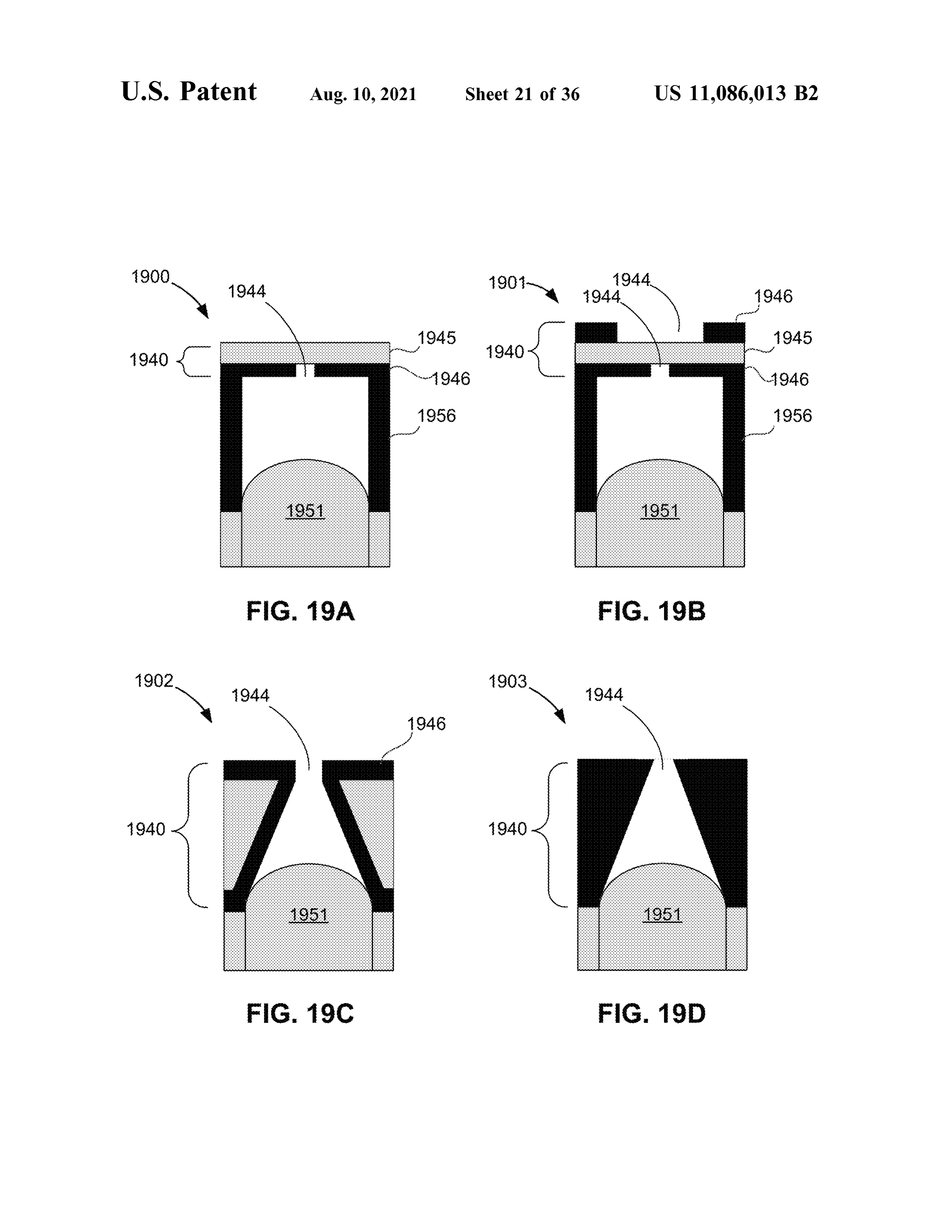
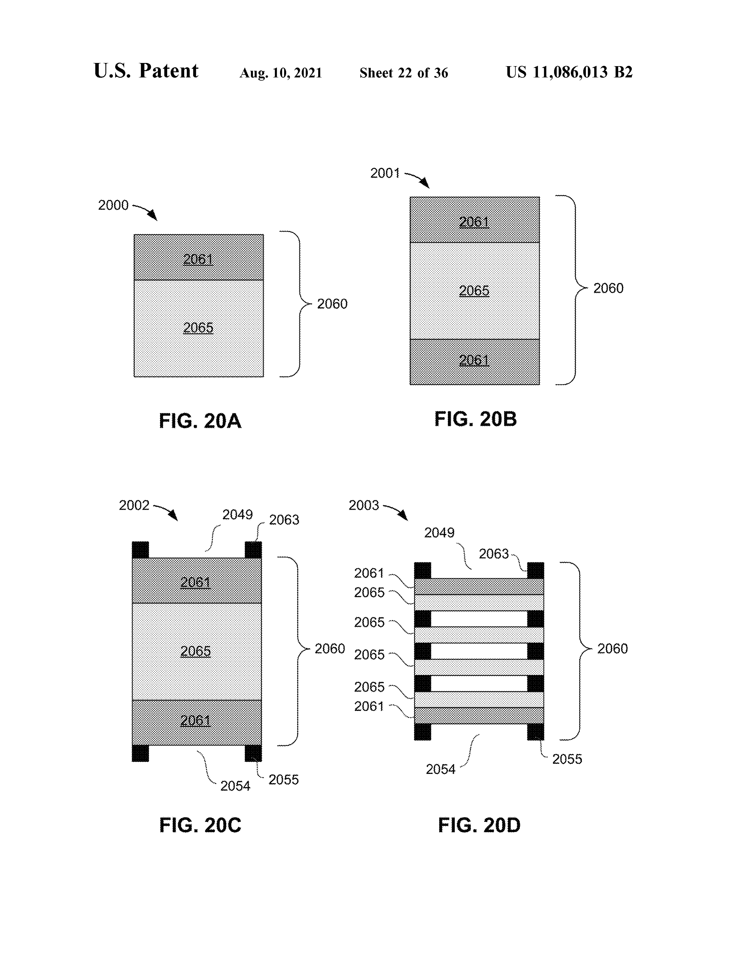
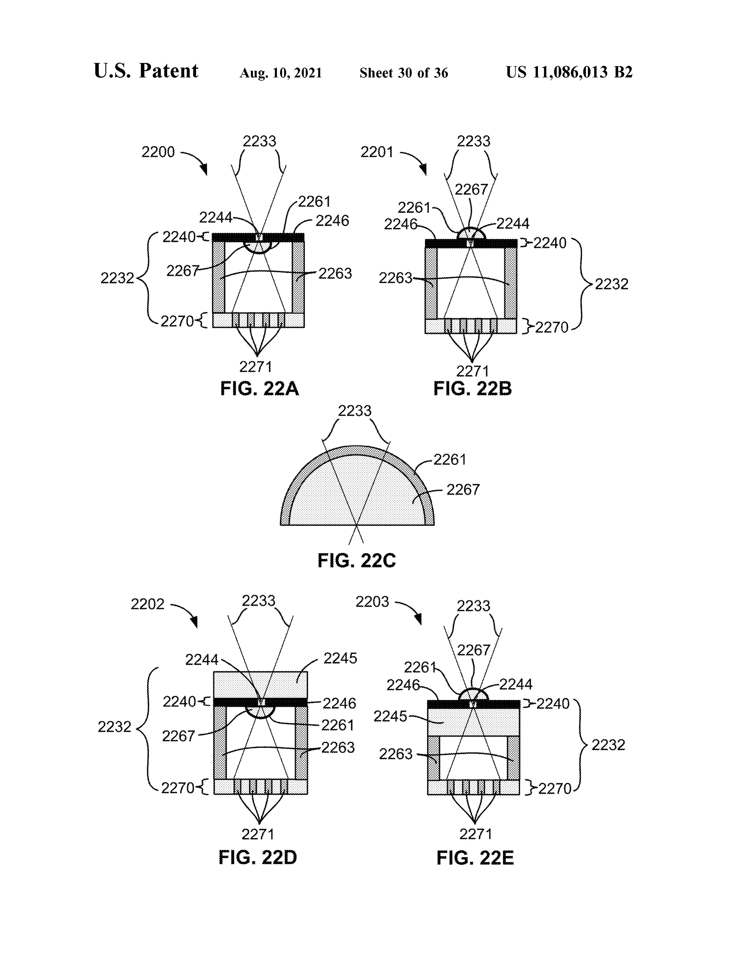
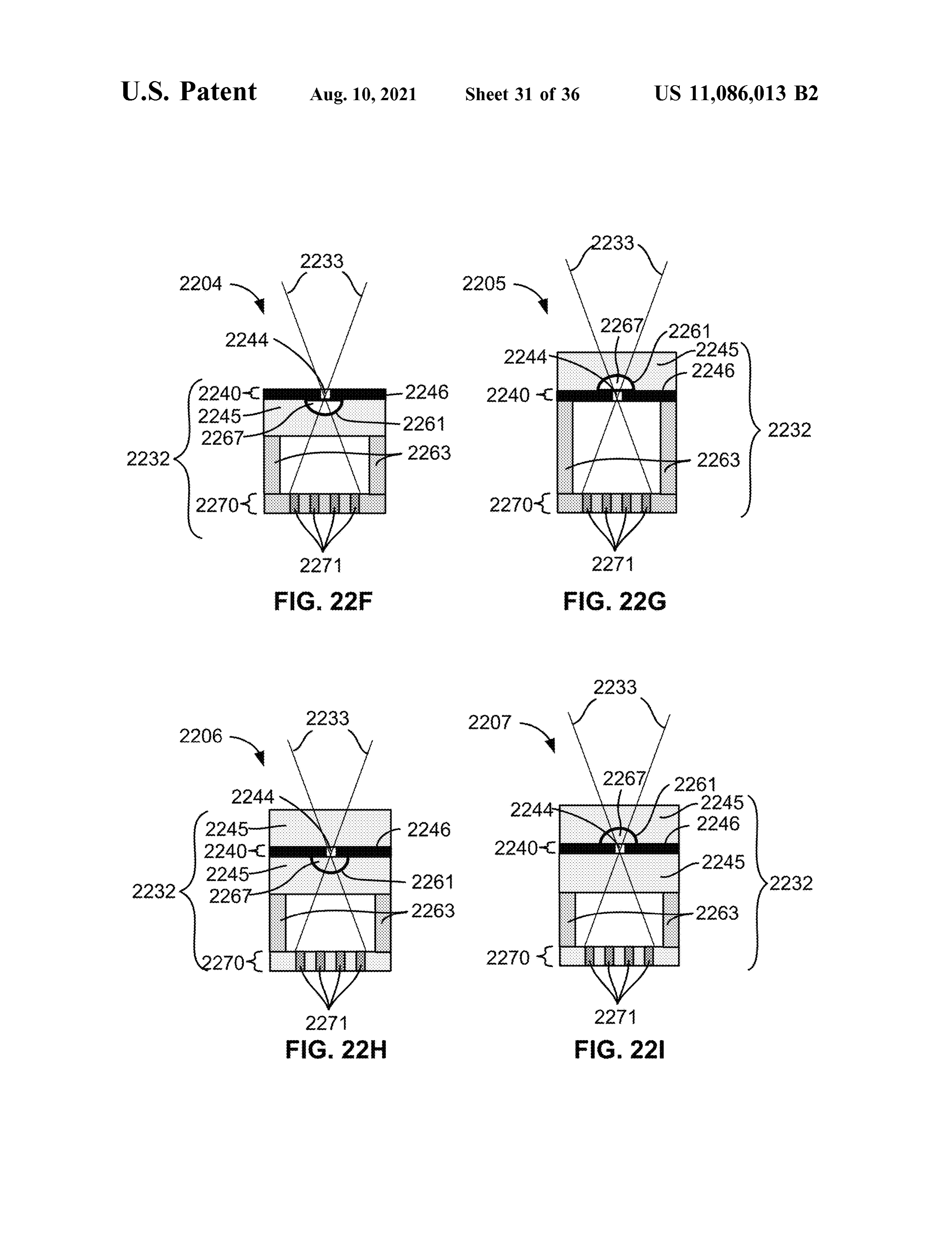
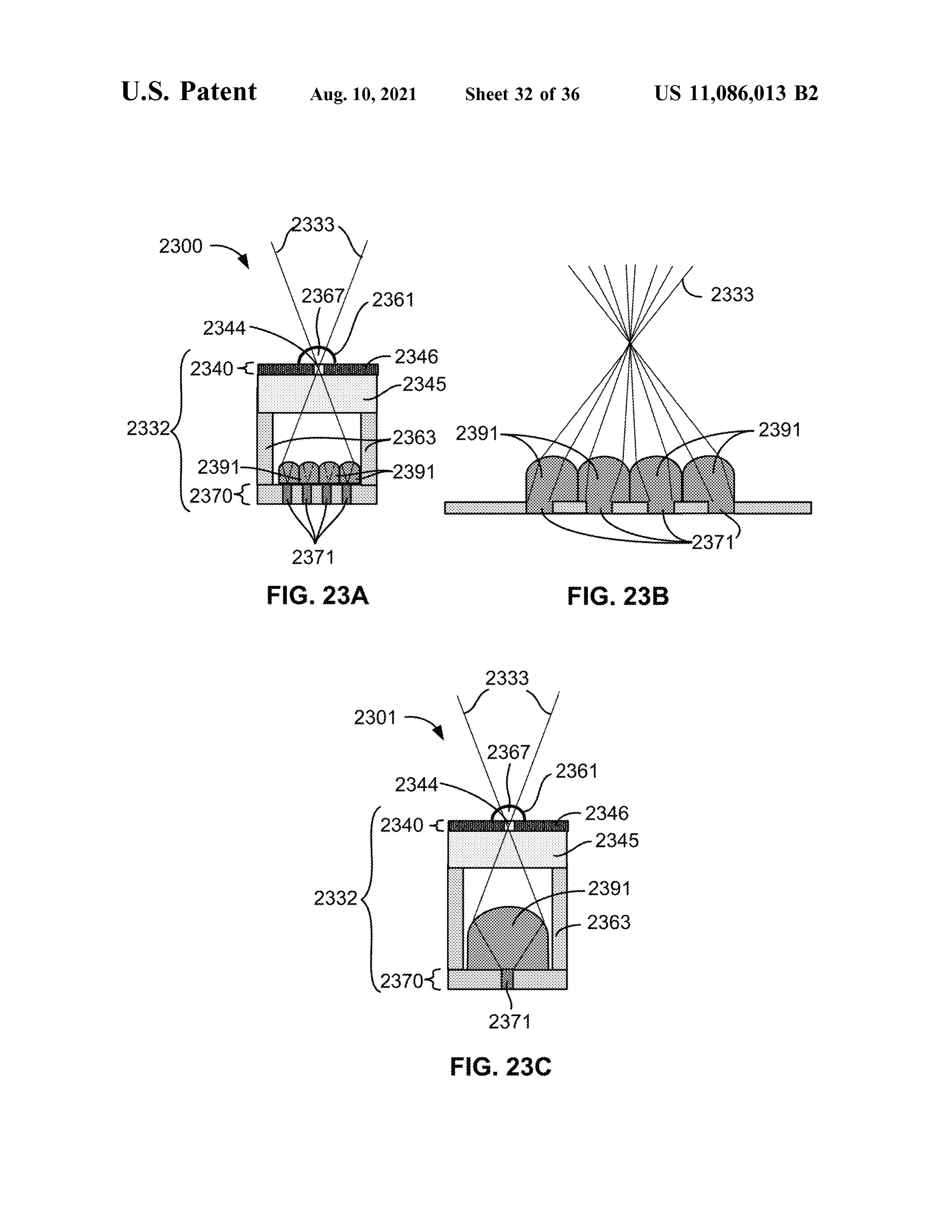
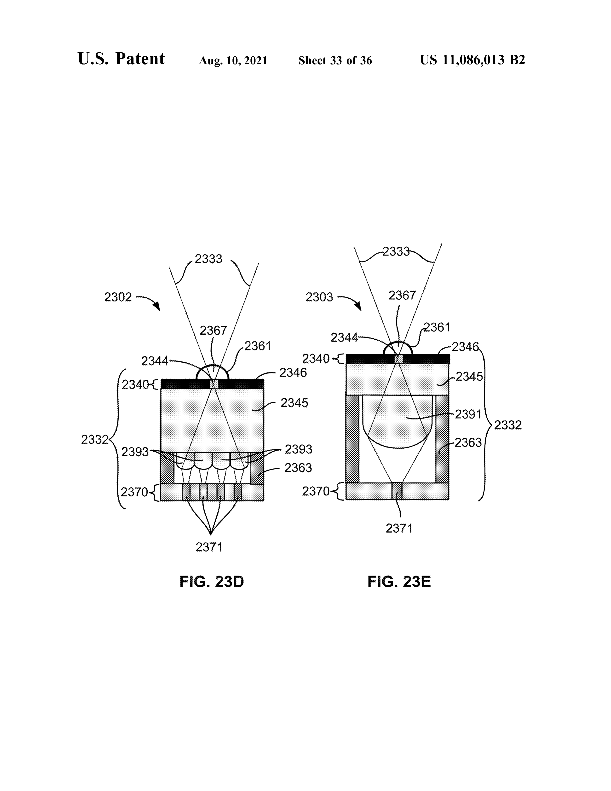
FIGS . 22A - 221 are simplified cross - sectional view dia disclosure modify light or optics instances, bulk imaging other according to the present radiation for an entire array grams of various hemispherical receiver structures for a receiver channel, according to some embodiments of the included of emitters or photosensors . Micro - optic structures can be present disclosure. as part of the array and can modify light differently FIGS . 23A- 23E are simplified cross -sectional view dia- 40 for different emitters and / or photosensors in the array. In grams of various bottom micro lens layers for a receiver some embodiments, there is one or more micro - optic ele channel, according to some embodiments of the present ments for each individual array element ( photosensor and / or disclosure . emitter ).
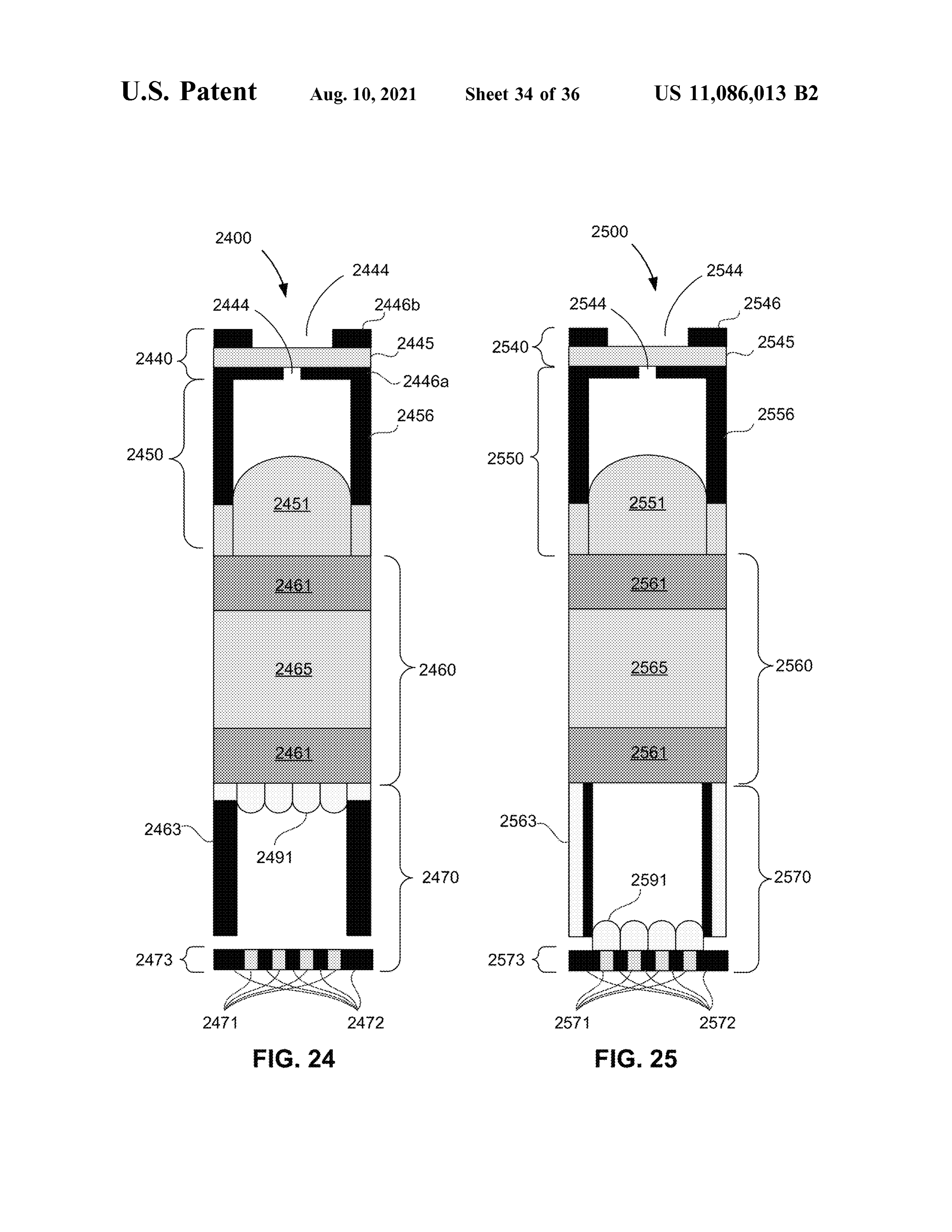
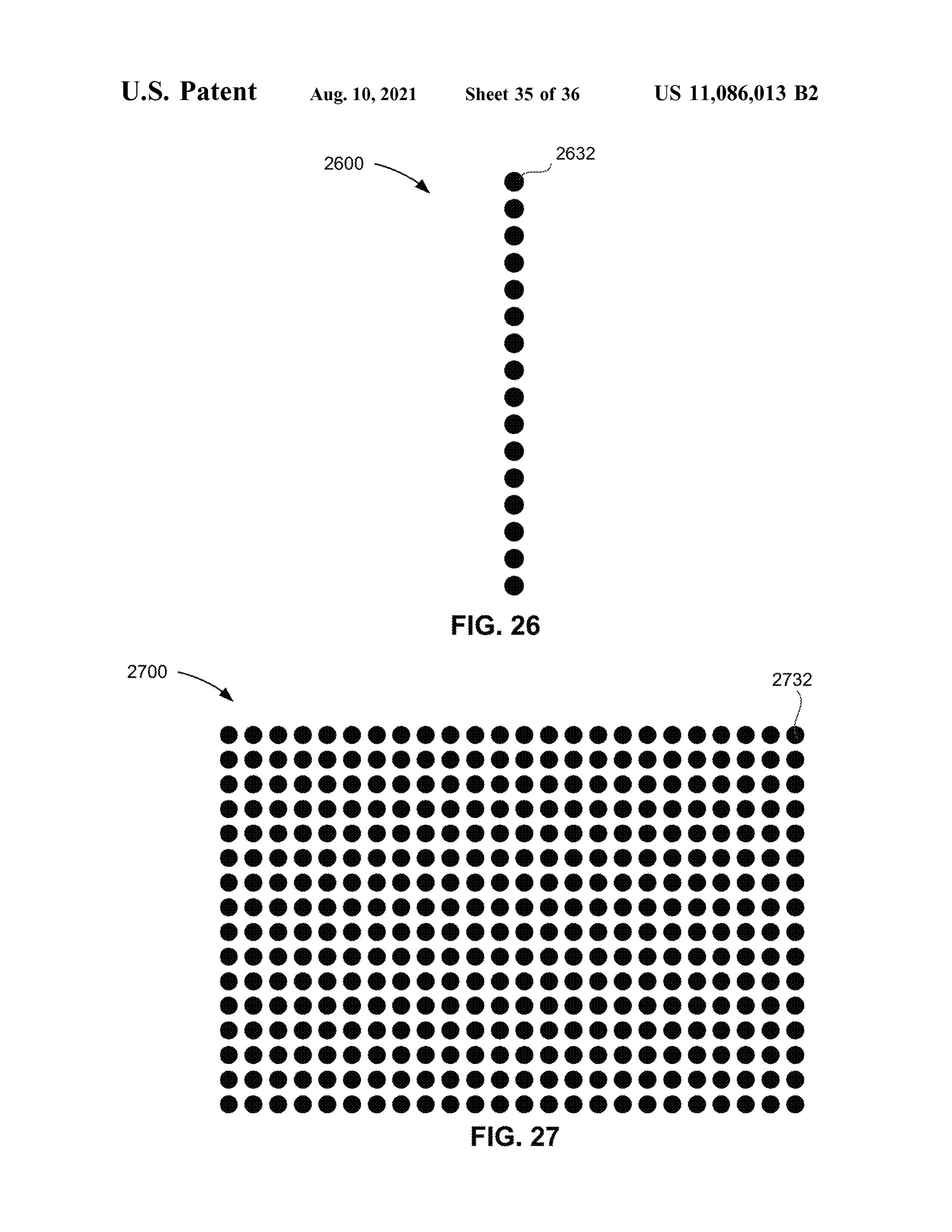
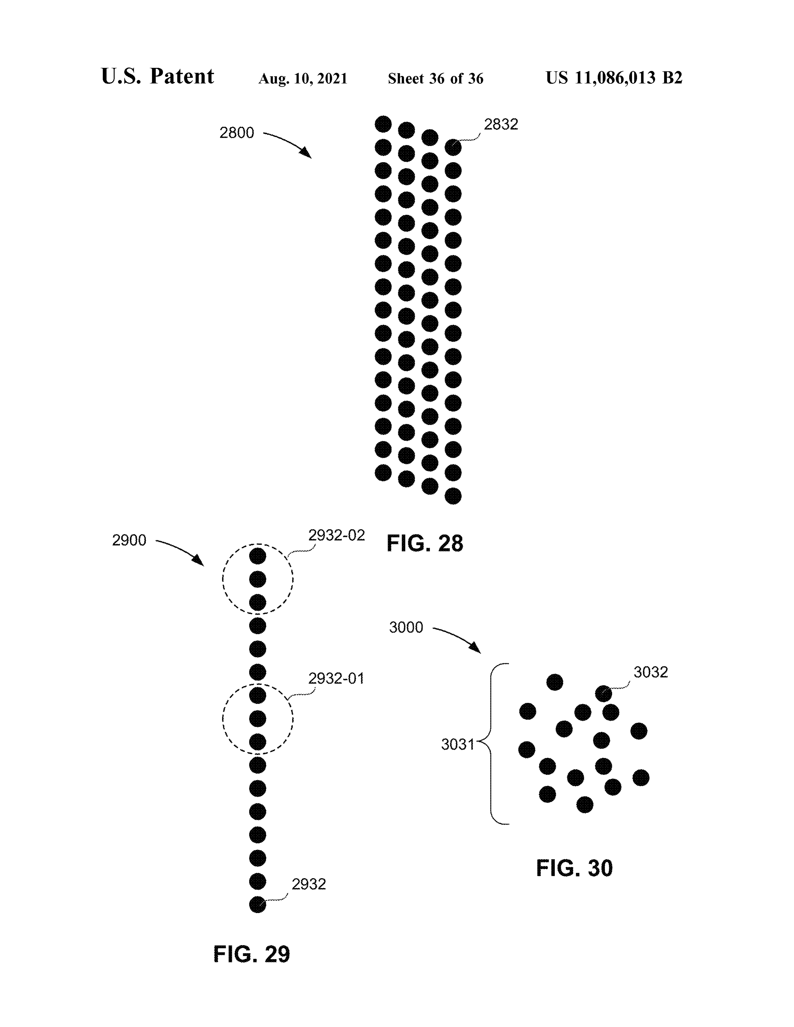
FIGS . 24 and 25 are simplified cross - sectional view In some embodiments, the optical imager system can be diagrams of exemplary receiver channels, according to some 45 an active system that can emit light into a field and then embodiments of the present disclosure . detect the emitted light after it has reflected off surfaces of FIGS . 26-30 are simplified top view diagrams of exem- an object in the field . An active optical imager system can plary micro -optical receiver arrays , according to some include a light transmission module in addition to a light embodiments of the present disclosure . sensing module, and be configured as a light ranging device . 50 The light transmission module can include a transmitter
DETAILED DESCRIPTION layer that is composed of an array of individual emitters where each emitter can be paired with a corresponding
Some embodiments of the disclosure pertain to optical micro - optic receiver channel in the light sensing module, or imager systems that can generate an image from ambient it can be a uniform illuminator that spreads light evenly light in a field and / or light emitted from an optical trans- 55 across the scene with no specific pairing between individual mitter that has reflected off of an object in the field . For emitters and receiver channels. In some instances , the light instance, in some embodiments an optical imager system transmission module can include a micro - optic transmitter can be a passive system that does not actively illuminate a channel array to enhance light outputted from the array of scene or given area and instead detects ambient light in the emitters. During operation, light outputted by the array of scene or area reflected off of one or more objects in the scene 60 emitters (e.g. , laser pulses ) passes through the micro -optic or area . A passive optical imager system can include a light transmitter channel array and enters a bulk transmitter optic sensing module for receiving ambient light in the field . The having a large numerical aperture to better capture light from light sensing module can be a wide field -of- view , narrow- the micro -optic transmitter channel array. The light then band optical imaging system (WFNBI ) that collects imaging exits the bulk transmitter optic and illuminates a plurality of information . The light sensing module can include one or 65 spots at a distant field . The micro - optic transmitter channel more bulk receiver optics , a micro - optic receiver system , array can improve the brightness of beams emanating from and a system controller for operating the light sensing the bulk transmitter optic to provide enhanced spot illumi
Page 46
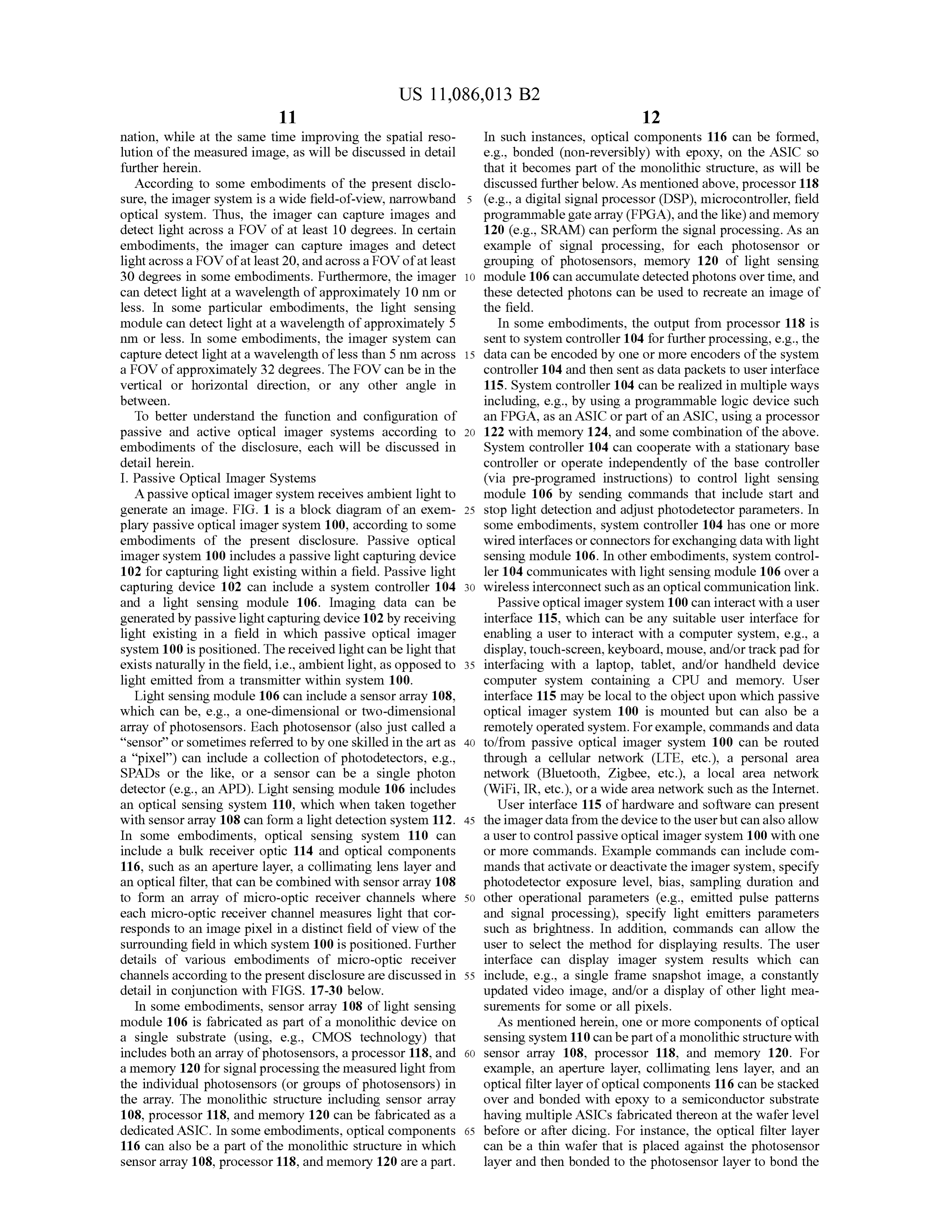
nation , while at the same time improving the spatial reso- In such instances , optical components 116 can be formed , lution of the measured image , as will be discussed in detail e.g. , bonded ( non - reversibly) with epoxy, on the ASIC so further herein . that it becomes part of the monolithic structure , as will be According to some embodiments of the present disclo- discussed further below . As mentioned above, processor 118 sure , the imager system is a wide field - of - view , narrowband 5 (e.g. , a digital signal processor (DSP ) , microcontroller, field optical system . Thus, the imager can capture images and programmable gate array ( FPGA ), and the like) and memory detect light across a FOV of at least 10 degrees . In certain 120 (e.g. , SRAM ) can perform the signal processing . As an embodiments, the imager can capture images and detect example of signal processing, for each photosensor or light across a FOV of at least 20 , and across a FOV of at least grouping of photosensors , memory 120 of light sensing 30 degrees in some embodiments. Furthermore, the imager 10 module 106 can accumulate detected photons over time , and can detect light at a wavelength of approximately 10 nm or these detected photons can be used to recreate an image of less . In some particular embodiments, the light sensing the field .
module can detect light at a wavelength of approximately 5 In some embodiments, the output from processor 118 is nm or less . In some embodiments , the imager system can sent to system controller 104 for further processing, e.g. , the capture detect light at a wavelength of less than 5 nm across 15 data can be encoded by one or more encoders of the system a FOV of approximately 32 degrees. The FOV can be in the controller 104 and then sent as data packets to user interface vertical or horizontal direction, or any other angle in 115. System controller 104 can be realized in multiple ways between . including, e.g. , by using a programmable logic device such To better understand the function and configuration of an FPGA, as an ASIC or part of an ASIC , using a processor passive and active optical imager systems according to 20 122 with memory 124 , and some combination of the above . embodiments of the disclosure, each will be discussed in System controller 104 can cooperate with a stationary base detail herein . controller or operate independently of the base controller I. Passive Optical Imager Systems ( via pre -programed instructions) to control light sensing A passive optical imager system receives ambient light to module 106 by sending commands that include start and generate an image . FIG . 1 is a block diagram of an exem- 25 stop light detection and adjust photodetector parameters. In plary passive optical imager system 100 , according to some some embodiments , system controller 104 has one or more embodiments of the present disclosure . Passive optical wired interfaces or connectors for exchanging data with light imager system 100 includes a passive light capturing device sensing module 106. In other embodiments, system control 102 for capturing light existing within a field . Passive light ler 104 communicates with light sensing module 106 over a capturing device 102 can include a system controller 104 30 wireless interconnect such as an optical communication link . and a light sensing module 106. Imaging data can be Passive optical imager system 100 can interact with a user generated by passive light capturing device 102 by receiving interface 115 , which can be any suitable user interface for light existing in a field in which passive optical imager enabling a user to interact with a computer system , e.g. , a system 100 is positioned . The received light can be light that display, touch - screen , keyboard , mouse , and / or track pad for exists naturally in the field, i.e. , ambient light, as opposed to 35 interfacing with a laptop , tablet, and / or handheld device light emitted from a transmitter within system 100 . computer system containing a CPU and memory. User Light sensing module 106 can include a sensor array 108 , interface 115 may be local to the object upon which passive which can be , e.g. , a one - dimensional or two - dimensional optical imager system 100 is mounted but can also be a array of photosensors . Each photosensor ( also just called a remotely operated system . For example , commands and data “ sensor” or sometimes referred to by one skilled in the art as 40 to / from passive optical imager system 100 can be routed a “ pixel” ) can include a collection of photodetectors, e.g. , through a cellular network ( LTE , etc. ), a personal area SPADs or the like , or a sensor can be a single photon network (Bluetooth , Zigbee , etc. ) , a local area network detector ( e.g. , an APD ) . Light sensing module 106 includes (WiFi, IR , etc. ), or a wide area network such as the Internet. an optical sensing system 110 , which when taken together User interface 115 of hardware and software can present with sensor array 108 can form a light detection system 112. 45 the imager data from the device to the user but can also allow In some embodiments, optical sensing system 110 can a user to control passive optical imager system 100 with one include a bulk receiver optic 114 and optical components or more commands. Example commands can include com 116 , such as an aperture layer, a collimating lens layer and mands that activate or deactivate the imager system , specify an optical filter, that can be combined with sensor array 108 photodetector exposure level , bias , sampling duration and to form an array of micro - optic receiver channels where 50 other operational parameters (e.g. , emitted pulse patterns each micro - optic receiver channel measures light that cor- and signal processing ) , specify light emitters parameters responds to an image pixel in a distinct field of view of the such as brightness. In addition, commands can allow the surrounding field in which system 100 is positioned . Further user to select the method for displaying results. The user details of various embodiments of micro -optic receiver interface can display imager system results which can channels according to the present disclosure are discussed in 55 include, e.g. , a single frame snapshot image, a constantly detail in conjunction with FIGS . 17-30 below . updated video image , and / or a display of other light mea In some embodiments, sensor array 108 of light sensing surements for some or all pixels .
module 106 is fabricated as part of a monolithic device on As mentioned herein , one or more components of optical a single substrate (using , e.g. , CMOS technology ) that sensing system 110 can be part of a monolithic structure with includes both an array of photosensors, a processor 118 , and 60 sensor array 108 , processor 118 , and memory 120. For a memory 120 for signal processing the measured light from example, an aperture layer, collimating lens layer, and an the individual photosensors ( or groups of photosensors ) in optical filter layer of optical components 116 can be stacked the array. The monolithic structure including sensor array over and bonded with epoxy to a semiconductor substrate 108 , processor 118 , and memory 120 can be fabricated as a having multiple ASICs fabricated thereon at the wafer level dedicated ASIC . In some embodiments , optical components 65 before or after dicing . For instance , the optical filter layer 116 can also be a part of the monolithic structure in which can be a thin wafer that is placed against the photosensor sensor array 108 , processor 118 , and memory 120 are a part. layer and then bonded to the photosensor layer to bond the
Page 47
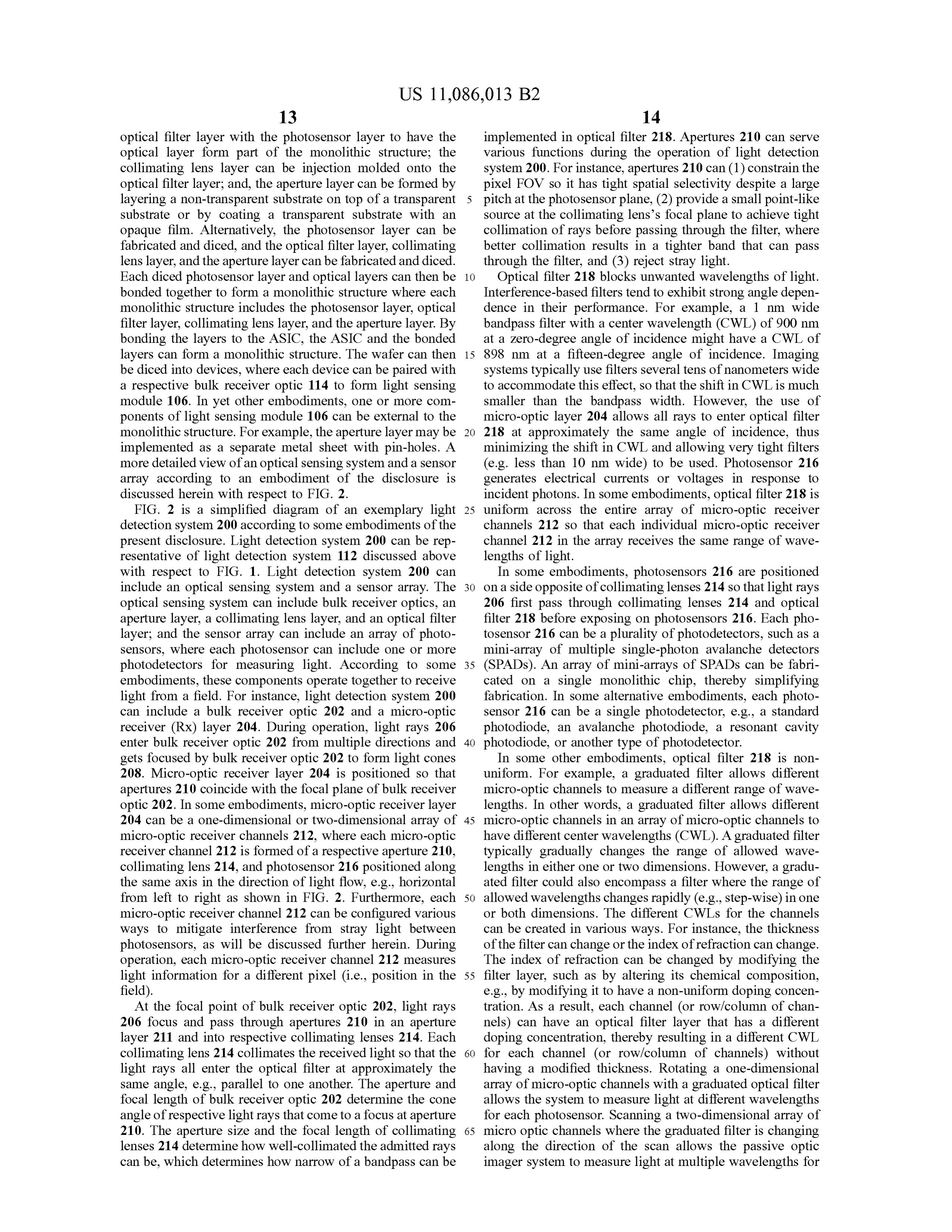
optical filter layer with the photosensor layer to have the implemented in optical filter 218. Apertures 210 can serve optical layer form part of the monolithic structure ; the various functions during the operation of light detection collimating lens layer can be injection molded onto the system 200. For instance, apertures 210 can ( 1 ) constrain the optical filter layer ; and, the aperture layer can be formed by pixel FOV so it has tight spatial selectivity despite a large layering a non - transparent substrate on top of a transparent 5 pitch at the photosensor plane, ( 2 ) provide a small point- like substrate or by coating a transparent substrate with an source at the collimating lens's focal plane to achieve tight opaque film . Alternatively, the photosensor layer can be collimation of rays before passing through the filter, where fabricated and diced , and the optical filter layer, collimating better collimation results in a tighter band that can pass lens layer, and the aperture layer can be fabricated and diced . through the filter, and ( 3 ) reject stray light. Each diced photosensor layer and optical layers can then be 10 Optical filter 218 blocks unwanted wavelengths of light. bonded together to form a monolithic structure where each Interference -based filters tend to exhibit strong angle depen monolithic structure includes the photosensor layer, optical dence in their performance. For example, a 1 nm wide filter layer, collimating lens layer, and the aperture layer. By bandpass filter with a center wavelength (CWL ) of 900 nm bonding the layers to the ASIC , the ASIC and the bonded at a zero -degree angle of incidence might have a CWL of layers can form a monolithic structure . The wafer can then 15 898 nm at a fifteen -degree angle of incidence . Imaging be diced into devices, where each device can be paired with systems typically use filters several tens of nanometers wide a respective bulk receiver optic 114 to form light sensing to accommodate this effect, so that the shift in CWL is much module 106. In yet other embodiments, one or more com- smaller than the bandpass width . However, the use of ponents of light sensing module 106 can be external to the micro - optic layer 204 allows all rays to enter optical filter monolithic structure . For example, the aperture layer may be 20 218 at approximately the same angle of incidence , thus implemented as a separate metal sheet with pin - holes. A minimizing the shift in CWL and allowing very tight filters more detailed view of an optical sensing system and a sensor (e.g. less than 10 nm wide ) to be used . Photosensor 216 array according to an embodiment of the disclosure is generates electrical currents or voltages in response to discussed herein with respect to FIG . 2 . incident photons. In some embodiments, optical filter 218 is FIG . 2 is a simplified diagram of an exemplary light 25 uniform across the entire array of micro -optic receiver detection system 200 according to some embodiments of the channels 212 so that each individual micro -optic receiver present disclosure . Light detection system 200 can be rep- channel 212 in the array receives the same range of wave resentative of light detection system 112 discussed above lengths of light.
with respect to FIG . 1. Light detection system 200 can In some embodiments, photosensors 216 are positioned include an optical sensing system and a sensor array. The 30 on a side opposite of collimating lenses 214 so that light rays optical sensing system can include bulk receiver optics , an 206 first pass through collimating lenses 214 and optical aperture layer, a collimating lens layer, and an optical filter filter 218 before exposing on photosensors 216. Each pho layer; and the sensor array can include an array of photo- tosensor 216 can be a plurality of photodetectors, such as a sensors , where each photosensor can include one or more mini-array of multiple single -photon avalanche detectors photodetectors for measuring light. According to some 35 (SPADs). An array of mini- arrays of SPADs can be fabri embodiments, these components operate together to receive cated on a single monolithic chip , thereby simplifying light from a field . For instance, light detection system 200 fabrication . In some alternative embodiments, each photo can include a bulk receiver optic 202 and a micro -optic sensor 216 can be a single photodetector, e.g. , a standard receiver ( Rx) layer 204. During operation , light rays 206 photodiode, an avalanche photodiode, a resonant cavity enter bulk receiver optic 202 from multiple directions and 40 photodiode, or another type of photodetector. gets focused by bulk receiver optic 202 to form light cones In some other embodiments, optical filter 218 is non 208. Micro - optic receiver layer 204 is positioned so that uniform . For example, a graduated filter allows different apertures 210 coincide with the focal plane of bulk receiver micro - optic channels to measure a different range of wave optic 202. In some embodiments, micro - optic receiver layer lengths. In other words, a graduated filter allows different 204 can be a one - dimensional or two - dimensional array of 45 micro - optic channels in an array of micro - optic channels to micro - optic receiver channels 212 , where each micro -optic have different center wavelengths ( CWL ) . A graduated filter receiver channel 212 is formed of a respective aperture 210 , typically gradually changes the range of allowed wave collimating lens 214 , and photosensor 216 positioned along lengths in either one or two dimensions . However, a gradu the same axis in the direction of light flow , e.g. , horizontal ated filter could also encompass a filter where the range of from left to right as shown in FIG . 2. Furthermore , each 50 allowed wavelengths changes rapidly (e.g. , step - wise) in one micro - optic receiver channel 212 can be configured various or both dimensions. The different CWLs for the channels ways to mitigate interference from stray light between can be created in various ways . For instance, the thickness photosensors, as will be discussed further herein . During of the filter can change or the index of refraction can change . operation , each micro -optic receiver channel 212 measures The index of refraction can be changed by modifying the light information for a different pixel (i.e. , position in the 55 filter layer, such as by altering its chemical composition , field ). e.g. , by modifying it to have a non -uniform doping concen At the focal point of bulk receiver optic 202 , light rays tration . As a result, each channel (or row / column of chan 206 focus and pass through apertures 210 in an aperture nels ) can have an optical filter layer that has a different layer 211 and into respective collimating lenses 214. Each doping concentration, thereby resulting in a different CWL collimating lens 214 collimates the received light so that the 60 for each channel ( or row / column of channels ) without light rays all enter the optical filter at approximately the having a modified thickness. Rotating a one - dimensional same angle, e.g. , parallel to one another. The aperture and array of micro - optic channels with a graduated optical filter focal length of bulk receiver optic 202 determine the cone allows the system to measure light at different wavelengths angle of respective light rays that come to a focus at aperture for each photosensor. Scanning a two - dimensional array of 210. The aperture size and the focal length of collimating 65 micro optic channels where the graduated filter is changing lenses 214 determine how well - collimated the admitted rays along the direction of the scan allows the passive optic can be , which determines how narrow of a bandpass can be imager system to measure light at multiple wavelengths for
Page 48
each position in space , but uses multiple photodetectors in 308 can have a different filter thickness than micro -optic the photosensor to do so . Such optical systems using gradu- receiver channels 306 and 310 and thus detect a different ated filters require synchronization of the photosensor sam- wavelength of light . During a first- time interval, the micro pling so that different wavelength measurements are taken optic receiver channels 304 and 308 measure the intensity of for the same photosensor with the same field -of - view . Imag- 5 a first wavelength of light for two pixels respectively. In ing systems that differentiate between many different wave- some embodiments, the hyperspectral passive optic imager lengths are sometimes referred to as hyperspectral imagers . system moves or rotates the micro - optic receiver layer so A hyperspectral imager often requires that light from the that during a second- time interval, micro - optic receiver wavelengths of interest all be focused in approximately the channels 306 and 310 measure the intensity of a second same plane. This can be achieved by using an achromatic, 10 wavelength of light for the same two pixels respectively. In apochromatic, superachromatic, or similar lens that is other embodiments, a hyperspectral passive optic imager designed to limit the effects of chromatic aberration . system according to the disclosure can include a stationary Hyperspectral imagers collect information from multiple micro - optic receiver layer and scan a moving target. wavelength bands across the electromagnetic spectrum . The II . Active Optical Imager Systems absolute or relative intensities of the wavelength bands can 15 As discussed herein , optical imager systems can also be provide information about chemical concentrations. For configured as active optical imager systems. Active optical example , chlorophyll content of certain crops can be esti- imager systems can differ from passive optical imager mated using only a few wavelength bands . Similar tech- systems in that active optical imager systems emit their own niques can be used to find valuable minerals or identify light into a field and detect the emitted light after it has toxins . Spectral information can also be used to assist in the 20 reflected off surface( s ) of an object in the field . In some classification of pedestrians, automobiles, and other objects embodiments, active optical imager systems can be utilized similarly encountered in an automotive environment. as LIDAR devices where emitted and received , reflected A graduated neutral -density filter has a transmission that light can be correlated to determine a distance to the object varies spatially across the filter, but the transmission is from which the emitted light was reflected . A better under largely independent of wavelength (e.g. just as transmissive 25 standing of an active optical imager system can be ascer to red light as to blue light) at any given location . In a tained with reference to FIG . 4 .
scanning imaging system , a graduated neutral -density filter FIG . 4 illustrates a block diagram of a LIDAR system 400 can be used to image the same point in space with varying according to some embodiments of the present disclosure . degrees of attenuation , thereby enabling a composite mea- LIDAR system 400 can include a light ranging device 402 surement with higher dynamic range than would achievable 30 and a user interface 415. Light ranging device 402 can with a non - graduated filter. A better understanding of a include a ranging system controller 404 , a light transmission micro - optic receiver layer with graduated filter can be (Tx ) module 406 and a light sensing (Rx) module 408 . achieved with reference to FIGS . 3A and 3B . Ranging data can be generated by light ranging device 402 FIGS . 3A and 3B are perspective views of a simplified by transmitting one or more light pulses 410 from the light diagram of different embodiments of micro - optic receiver 35 transmission module 406 to objects in a field of view layers with graduated filter layers, according to some surrounding light ranging device 402. Reflected portions embodiments of the present disclosure. Specifically, FIG . 412 of the transmitted light are then detected by light sensing 3A is a perspective view of a simplified diagram of a module 408 after some delay time . Based on the delay time , micro -optic receiver layer 300 with a graduated filter layer the distance to the reflecting surface can be determined . 302 , and FIG . 3B is a perspective view of a simplified 40 Other ranging methods can be employed as well , e.g. diagram of a micro - optic receiver layer 301 with a graduated continuous wave , Doppler, and the like. filter layer 312. As illustrated in FIGS . 3A and 3B , micro- Tx module 406 includes an emitter array 414 , which can optic receiver layer 300 and 301 each includes four micro- be a one - dimensional or two - dimensional array of emitters , optic receiver channels 304 , 306 , 308 and 310 arranged in and a Tx optical system 416 , which when taken together two dimensions as a 2x2 array. Although FIGS . 3A and 3B 45 with emitter array 414 can form a light emission system 438 . illustrate embodiments having only 2x2 arrays , one skilled Tx optical system 416 can include a bulk transmitter optic in the art understands that such embodiments are not limit- that is image - space telecentric. In some embodiments, Tx ing and that other embodiments can be configured to have optical system 416 can further include one or more micro any number of micro - optic receiver channels. It is to be optic structures that increase the brightness of beams ema appreciated that in these diagrams, the thicknesses of filter 50 nating from the bulk transmitter optic as discussed herein layers 302 and 312 and the thicknesses of the surrounding with respect to FIGS . 11-14 and / or for beam shaping , beam layers, which are not drawn to scale , should be interpreted steering or the like. Emitter array 414 or the individual as the thicknesses of layers of refractive material in an emitters can be laser sources . Tx module 406 can further interference filter. As these thicknesses change, the charac- include an optional processor 418 and memory 420 , teristics (e.g. passband CWL ) of the interference filter 55 although in some embodiments these computing resources change. These embodiments can be used in a hyperspectral can be incorporated into ranging system controller 404. In passive optic imager system . some embodiments, a pulse coding technique can be used , As shown in FIGS . 3A and 3B , graduated filter layer 302 e.g. , Barker codes and the like . In such cases , memory 420 has gradually increasing thickness in one dimension across can store pulse - codes that indicate when light should be multiple columns of micro -optic receiver channels, and 60 transmitted. In some embodiments, the pulse - codes are graduated filter layer 312 has a step - wise - increasing thick- stored as a sequence of integers stored in memory . ness in one dimension that has a constant thickness for each Light sensing module 408 can be substantially similar in micro - optic receiver channel. Micro -optic receiver channels construction to light sensing module 106 discussed herein 304 and 308 have the same filter thickness and detect the with respect to FIG . 1. Thus, details of processor 422 , same wavelength of light. Micro - optic receiver channels 306 65 memory 424 , sensor array 426 , and Rx optical system 428 and 310 have the same filter thickness and detect the same ( when taken together with sensor array 426 can form a light wavelength of light. Micro -optic receiver channels 304 and detection system 436 ) can be referenced herein with respect
Page 49
to FIG . 1 , and only differences with respect to those com- with respect to FIGS . 5A and 5B , while exemplary scanning ponents are discussed herein for brevity. For LIDAR system LIDAR devices are discussed further herein with respect to 400 , each photosensor sensor ( e.g. , a collection of SPADs) FIGS . 6A , 6B , and 7 .
of sensor array 426 can correspond to a particular emitter of LIDAR system 400 can interact with one or more instan emitter array 414 , e.g. , as a result of a geometrical configu- 5 tiations of a user interface 415. The different instantiations ration of light sensing module 408 and Tx module 406. For can vary and can include, but not be limited to , a computer example , in some embodiments, emitter array 414 can be system with a monitor, keyboard, mouse , CPU and memory ; arranged along the focal plane of the bulk transmitter optic a touch - screen in an automobile or other vehicle ; a handheld such that each illuminating beam projected from the bulk device with a touch - screen ; or any other appropriate user transmitter optic into the field ahead of the system is 10 interface . User interface 415 can be local to the object upon substantially the same size and geometry as the field of view which LIDAR system 400 is mounted but can also be a of a corresponding receiver channel at any distance from the remotely operated system . For example , commands and data system beyond an initial threshold distance . to / from LIDAR system 400 can be routed through a cellular In some embodiments, processor 418 can perform signal network (LTE , etc. ), a personal area network (Bluetooth , processing of the raw histograms from the individual photon 15 Zigbee , etc. ) , a local area network (WiFi, IR , etc.), or a wide detectors ( or groups of detectors ) in the array. As an example area network such as the Internet. of signal processing, for each photon detector or grouping of User interface 415 of hardware and software can present photon detectors, memory 424 ( e.g. , SRAM ) can accumulate the LIDAR data from the device to the user or to a vehicle counts of detected photons over successive time bins , and control unit (not shown) but can also allow a user to control these time bins taken together can be used to recreate a time 20 LIDAR system 400 with one or more commands . series of the reflected light pulse ( i.e. , a count of photons vs. Example commands can include commands that activate or time ) . This time- series of aggregated photon counts is deactivate the LIDAR system , specify photodetector expo referred to herein as an intensity histogram (or just histo- sure level , bias , sampling duration and other operational gram ). Processor 418 can implement matched filters and parameters (e.g. , emitted pulse patterns and signal process peak detection processing to identify return signals in time . 25 ing ) , specify light emitters parameters such as brightness. In In addition , Processor 418 can accomplish certain signal addition , commands can allow the user to select the method processing techniques ( e.g. , by processor 422 ) , such as for displaying results . The user interface can display LIDAR multi - profile matched filtering to help recover a photon time system results which can include , e.g. , a single frame series that is less susceptible to pulse shape distortion that snapshot image , a constantly updated video image , and / or a can occur due to SPAD saturation and quenching. In some 30 display of other light measurements for some or all pixels . embodiments, all or parts of such filtering can be performed In some embodiments, user interface 415 can track distances by processor 458 , which may be embodied in an FPGA. (proximity ) of objects from the vehicle , and potentially In some embod nts , the photon time series output from provide alerts to a driver or provide such tracking informa processor 418 are sent to ranging system controller 404 for tion for analytics of a driver's performance. further processing, e.g. , the data can be encoded by one or 35 In some embodiments, for example where LIDAR system more encoders of ranging system controller 404 and then 400 is used for vehicle navigation , user interface 415 can be sent as data packets to user interface 415. Ranging system a part of a vehicle control unit that receives output from , and controller 404 can be realized in multiple ways including , otherwise communicates with light ranging device 402 e.g. , by using a programmable logic device such an FPGA, and / or user interface 415 through a network , such as one of as an ASIC or part of an ASIC , using a processor 430 with 40 the wired or wireless networks described above. One or memory 432 , and some combination of the above . Ranging more parameters associated with control of a vehicle can be system controller 404 can cooperate with a stationary base modified by the vehicle control unit based on the received controller or operate independently of the base controller LIDAR data. For example, in a fully autonomous vehicle , ( via pre -programed instructions) to control light sensing LIDAR system 400 can provide a real time 3D image of the module 408 by sending commands that include start and 45 environment surrounding the car to aid in navigation in stop light detection and adjust photodetector parameters. conjunction with GPS and other data . In other cases , LIDAR Similarly, ranging system controller 404 can control light system 400 can be employed as part of an advanced driver transmission module 406 by sending commands, or relaying assistance system ( ADAS ) or as part of a safety system that, commands from the base controller, that include start and e.g. , can provide 3D image data to any number of different stop light emission controls and controls that can adjust 50 systems , e.g. , adaptive cruise control, automatic parking, other light -emitter parameters ( e.g. , pulse codes ) . In some driver drowsiness monitoring, blind spot monitoring , colli embodiments, ranging system controller 404 has one or sion avoidance systems , etc. When user interface 415 is more wired interfaces or connectors for exchanging data implemented as part of a vehicle control unit, alerts can be with light sensing module 408 and with light transmission provided to a driver or tracking of a proximity of an object module 406. In other embodiments, ranging system control- 55 can be tracked .
ler 404 communicates with light sensing module 408 and A. Solid State Architecture light transmission module 406 over a wireless interconnect LIDAR systems , according to some embodiments of the such as an optical communication link . present disclosure, can be configured as a solid state LIDAR Light ranging device 402 can be used in both stationary system that has a stationary architecture. Such LIDAR and a scanning architectures . Electric motor 434 is an 60 systems do not rotate , and thus do not need a separate motor, optional component in LIDAR system 400 that can be used e.g. , electric motor 434 in FIG . 4 , to rotate the sensor and to rotate system components, e.g. , the Tx module 406 and transmitter modules. Example solid state LIDAR systems Rx module 408 , as part of a scanning LIDAR architecture. are shown in FIGS . 5A and 5B .
The system controller 404 can control the electric motor 434 FIGS . 5A and 5B are simple illustrations of exemplary and can start rotation , stop rotation and vary the rotation 65 implementations of solid state LIDAR systems. Specifically, speed as needed to implement a scanning LIDAR system . FIG . 5A illustrates an implementation 500 where solid state Exemplary stationary LIDAR devices are discussed below LIDAR systems 502a - d are implemented at the outer
Page 50
regions of a road vehicle 505 , such as an automobile, rotating column or platform or through the use of other according to some embodiments of the present disclosure; mechanical means , such as galvanometers. Chip -based and FIG . 5B illustrates an implementation 501 where solid beam steering techniques can also be employed , e.g. , by state LIDAR systems 504a - b are implemented on top of using microchips that employ one or more MEMS based road vehicle 505 , according to some embodiments of the 5 reflectors, e.g. , such as a digital micromirror (DMD ) device , present disclosure . In each implementation, the number of a digital light processing (DLP ) device , and the like . In some LIDAR systems , the placement of the LIDAR systems , and embodiments , the scanning can be effectuated through non the fields of view of each LIDAR system can be chosen to mechanical means , e.g. , by using electronic signals to steer obtain a majority of, if not the entirety of, a 360 degree field of view of the environment surrounding the vehicle . Auto- 10 oneOther or more optical phased arrays.
embodiments can implement a scanning architec motive implementations for the LIDAR systems are chosen ture that scans through the entire 360 degrees of the envi herein merely for the sake of illustration and the sensors ronment surrounding a vehicle . Such scanning LIDAR sys described herein may be employed in other types of vehicles, e.g. , boats, aircraft, trains, etc., as well as in a tems can repetitively rotate continuously through 360 variety of other applications where 3D depth images are 15 thus degrees inutilize a clockwise or counter -clockwise direction, and useful, such as medical imaging, mobile phones, augmented FIG . may a separate motor, e.g. , electric motor 434 in 4 , to rotate the sensor and transmitter modules. Exem reality, geodesy, geomatics, archaeology, geography, geol ogy , geomorphology, seismology, forestry, atmospheric plary rotating LIDAR systems are shown in FIGS . 6A and physics, laser guidance, airborne laser swath mapping 6B .
(ALSM) , and laser altimetry. 20 FIG . 6A is a top - down view of a simplified diagram of an With reference to FIG . 5A , solid state LIDAR systems exemplary scanning LIDAR system 600 implemented for a 502a - d can be mounted at the outer regions of a vehicle , near vehicle 605 , such as a car, and capable of continuous 360 the front and back fenders. LIDAR systems 502a - d can each degree scanning, according to some embodiments of the be positioned at a respective corner of vehicle 505 so that present disclosure . The output beam ( s ) of one or more light they are positioned near the outermost corners of vehicle 25 sources ( such as infrared or near - infrared pulsed IR lasers , 505. That way, LIDAR systems 502a - d can better measure not shown ) located in LIDAR system 600 , can be scanned, the distance of vehicle 505 from objects in the field at areas e.g. , rotated, to illuminate a continuous scene 620 around the 506a - d . Each solid state LIDAR system can face a different vehicle. In some embodiments, the scanning, represented by direction ( possibly with partially and / or non -overlapping rotation arrow 615 , can be implemented by any suitable fields of views between units ) so as to capture a composite 30 mechanical means discussed herein with respect to FIG . 5B , field of view that is larger than each unit is capable of e.g. , by mounting the light emitters to a rotating column or capturing on its own . Objects within the scene can reflect platform , or any other mechanical means , such as through portions of light pulses 510 that are emitted from LIDAR TX the use of galvanometers or chip -based steering techniques. module 508. One or more reflected portions 512 of light During operation, objects around vehicle 605 in any direc pulses 510 then travel back to LIDAR system 502a and can 35 tion and within the view of LIDAR system 600 can reflect be received by Rx module 509. Rx module 509 can be portions of light pulses 611 that are emitted from a trans disposed in the same housing as Tx module 508 . mitting module 608 in LIDAR system 600. One or more Although FIG . 5A illustrates four solid state LIDAR reflected portions 617 of light pulses 611 then travel back to systems mounted at the four corners of a vehicle , embodi- LIDAR system 600 and can be detected by its sensing ments are not limited to such configurations. Other embodi- 40 module 609. In some instances, sensing module 609 can be ments can have fewer or more solid state LIDAR systems disposed in the same housing as transmitting module 608 . mounted on other regions of a vehicle . For instance , LIDAR Although FIG . 6A illustrates solid state LIDAR systems systems can be mounted on a roof of a vehicle 505 , as shown mounted on a roof of a vehicle 605 , embodiments are not in FIG . 5B . In such embodiments, LIDAR systems can have limited to such configurations. Other embodiments can have a higher vantage point to better observe areas 506a - d around 45 solid state LIDAR systems mounted on other regions of a vehicle 505 . vehicle. For instance, LIDAR systems can be mounted at the B. Scanning Architecture corners of a vehicle , as shown in FIG . 6B . FIG . 6B illustrates In some embodiments, LIDAR systems according to the an implementation 601 where solid state LIDAR systems present disclosure can employ a scanning architecture in 604a - d are implemented at the outer regions of a road which the LIDAR system oscillates between an angle that is 50 vehicle , such as a car, according to some embodiments of the less than 360 degrees. For instance , LIDAR systems 504a - b present disclosure . In this implementation, each LIDAR in implementation 501 of FIG . 5B can each employ a system 604a - d can be a spinning LIDAR system that can scanning architecture to scan the entire scene in front of, measure distances around the full 360 degrees. However, and / or behind, vehicle 505 , e.g. , in area 514 between field of since at least some of those measurements will be measured view 506? and 506b and in area 516 between field of view 55 with respect to vehicle 605 , those measurements can be 506c and 506d . The output beam ( s ) of one or more light ignored . Thus, each LIDAR system 605a - d can only utilize sources ( not shown , but can be a variety of different suitable a subset of the measurements from 360 degree scanning, sources for emitting radiation including, but not limited to e.g. , only the angles covering regions 619a - d that do not lasers, in any wavelength spectrum suitable for LIDAR capture vehicle 605 are utilized .
systems , such as in the infrared , near - infrared , ultraviolet, 60 FIG . 7 is a simplified exemplary perspective view of a visible , e.g. , green laser wavelength spectrum , and the like ) LIDAR system 700 that employs a 360 scanning architec located in the scanning LIDAR systems , can be outputted as ture, according to some embodiments of the present disclo pulses of light and scanned , e.g. , rotated between an angle sure . In some embodiments , LIDAR system 700 can include that is less than 360 degrees, to illuminate a scene around the a light ranging device 701 that spins in a clockwise or vehicle. In some embodiments, the scanning, represented by 65 counter - clockwise direction to observe the surrounding field rotation arrows 514 and 516 , can be implemented by around a vehicle . System 700 can include a stationary mechanical means , e.g. , by mounting the light emitters to a housing 702 , an optically transparent window 704 , and a
Page 51
stationary lid 706 for providing protection for the internal for the sake of clarity ). Likewise , emitter 816 emits an components of LIDAR system 700 . illuminating beam 818 (also called an emitter channel) into Window 704 can extend fully around a periphery of the circular field of view 834. While not shown in FIG . 8 to stationary housing 702 , which can be configured to have a avoid complication, each emitter emits a corresponding cylindrical shape. The internal components of system 700 5 illuminating beam into its corresponding field of view can include light ranging device 701 , which can include a resulting in a 2D array of fields of view being illuminated rotating platform 708 and sensing and transmitting modules (21 distinct fields of view in this example ). 710 mounted on rotating platform 708. In some embodi- Each field of view that is illuminated by an emitter can be ments, light ranging device 701 is aligned with window 704 thought of as a pixel or spot in the corresponding 3D image such that modules 710 are positioned to emit and receive 10 that is produced from the ranging data . Each emitter channel light through window 704 , and that emitted light is not can be distinct to each emitter and be non -overlapping with emitted onto stationary housing 702 or stationary lid 706 . other emitter channels, i.e. , there is a one - to - one mapping For instance, in the aligned positioned , the horizontal center between the set of emitters and the set of non -overlapping of light ranging device 701 coincides with the horizontal fields or view . Thus, in the example of FIG . 8 , the system can center of window 704. Sensing and transmitting modules 15 sample 21 distinct points in the 3D space. A denser sampling 710 can be , for example, light sensing module 408 and light of points can be achieved by having a denser array of transmission module 406 , and can optionally include a heat emitters or by scanning angular position of the emitter sink (not shown) to cool the micro - optic layers. LIDAR beams over time such that one emitter can sample several system 700 can also include a system controller 712 ( e.g. , points in space . As described above, scanning can be accom controller 404 ) and electric motor 714 ( e.g. , motor 434 ) that 20 plished by rotating the entire emitter /sensor assembly. reside within stationary housing 702. Electric motor 714 Each sensor can be slightly offset from its neighbor and, rotates platform 708 , thereby rotating sensing and transmit- like the emitters described above, each sensor can see a ting modules 710 in a spinning manner, e.g. , continuously different field of view of the scene in front of the sensor. through 360 degrees in a clockwise or counter - clockwise Furthermore, each sensor's field of view substantially coin direction . System controller 712 can communicate with 25 cides with , e.g. , overlaps with and is the same size as a sensing and transmitting modules 710 using an optical respective emitter channel's field of view.
communication link 716. Optical communication link 716 In FIG . 8 , the distance between corresponding emitter allows sensing and transmitting modules 710 to communi- receiver channels is exaggerated relative to the distance to cate with stationary system controller 712 , which is objects in the field of view. In practice, the distance to the mechanically coupled to stationary housing 702 and does 30 objects in the field of few is much greater than the distance not rotate with platform 708 , through optical communication between corresponding emitter - receiver channels and thus link 716 without mechanical wear and tear. In some embodi- the path of light from the emitter to the object is approxi ments , system controller 712 can control the motor and mately parallel to the path of the reflected light back from start and stop light detection operations of LIDAR system the object to the sensor ( i.e. , it is almost “ back reflected ” ). 700. System controller 712 can include two or more stacked 35 Accordingly, there is a range of distances in front of the planar circuit boards arranged in a parallel relationship , system 800 over which the fields of view of individual which is discussed in more detail in commonly -owned and sensors and emitters are overlapped .
concurrently - filed Patent Application entitled “ Compact Because the fields of view of the emitters are overlapped Lidar System ” , which is herein incorporated by reference in with the fields of view of their respective sensors , each its entirety for all purposes. 40 receiver channel ideally can detect the reflected illumination III . Operation of Active Imager Systems beam that originates from its respective emitter channel with FIG . 8 is an illustrative example of the light transmission ideally no cross -talk , i.e. , no reflected light from other and detection operation for a light ranging system according illuminating beams is detected . Thus, each photosensor can to some embodiments. FIG . 8 shows a light ranging system correspond to a respective light source . For example, emitter 800 (e.g. , solid state or and / or scanning system) collecting 45 812 emits an illuminating beam 814 into the circular field of three - dimensional distance data of a volume or scene that view 832 and some of the illuminating beam reflects from surrounds the system . FIG . 8 is an idealized drawing to the object 830. Ideally, a reflected beam 824 is detected by highlight relationships between emitters and sensors, and sensor 822 only. Thus, emitter 812 and sensor 822 share the thus other components are not shown. same field of view, e.g. , field of view 832 , and form an Light ranging system 800 includes a light emitter array 50 emitter - sensor pair. Likewise, emitter 816 and sensor 826 810 and a light sensor array 820. The light emitter array 810 form an emitter - sensor pair, sharing field of view 834. While includes an array of light emitters, e.g. , an array of vertical- the emitter - sensor pairs are shown in FIG . 8 as being in the cavity surface -emitting lasers (VCSELs ) and the like , such same relative locations in their respective array , any emitter as emitter 812 and emitter 816. Light sensor array 820 can be paired with any sensor depending on the design of the includes an array of photosensors, e.g. , sensors 822 and 826. 55 optics used in the system .
The photosensors can be pixelated light sensors that employ, During a ranging measurement, the reflected light from for each photosensor, a set of discrete photodetectors such as the different fields of view distributed around the volume single photon avalanche diodes (SPADs) and the like . How- surrounding the LIDAR system is collected by the various ever, various embodiments can deploy other types of photon sensors and processed , resulting in range information for sensors . 60 any objects in each respective field of view. As described Each emitter can be slightly offset from its neighbor and above , a time -of -flight technique can be used in which the can be configured to transmit light pulses into a different light emitters emit precisely timed pulses , and the reflections field of view from its neighboring emitters, thereby illumi- of the pulses are detected by the respective sensors after nating a respective field of view associated with only that some elapsed time . The elapsed time between emission and emitter. For example , emitter 812 emits an illuminating 65 detection and the known speed of light is then used to beam 814 ( formed from one or more light pulses ) into the compute the distance to the reflecting surface . In some circular field of view 832 (the size of which is exaggerated embodiments , additional information can be obtained by the
Page 52
sensor to determine other properties of the reflecting surface object, thereby allowing a ranging measurement to the in addition to the range. For example, the Doppler shift of a object. Each of the N pulse trains can include one or more pulse can be measured by the sensor and used to compute the pulses from the light source (e.g. , VCSELs ) and correspond relative velocity between the sensor and the reflecting sur- to a different time interval that is triggered by a start signal . face . The pulse strength can be used to estimate the target 5 In some embodiments , the CPOS can wait for a specified reflectivity, and the pulse shape can be used to determine if time to allow a previous pulse train ( coded -pulse transmis the target is a hard or diffuse material. sion) to dissipate. The CPOS can then transmit a next pulse In some embodiments, the LIDAR system can be com- train of the N pulse trains of a measurement, where the N posed of a relatively large 2D array of emitter and receiver pulse trains form a code . Once a measurement is complete, channels and operate as a solid state LIDAR , i.e. , it can 10 e.g. , a last of the N pulse train has dissipated ( e.g. , after a obtain frames of range data without the need to scan the predetermined time expected for any reflections), the CPOS orientation of the emitters and / or sensors . In other embodi- can then start the first /next coded- pulse transmission using ments, the emitters and sensors can be scanned , e.g. , rotated the appropriate pulse -code. N can be an integer greater than about an axis , to ensure that the fields of view of the sets of one , e.g. , 2 , 3 , 4 , 5 , or higher. emitters and sensors sample a full 360 degree region (or 15 At 930 , optical detection can be started , e.g. , in response some useful fraction of the 360 degree region) of the to the start signal that triggers the pulse train to be trans surrounding volume. The range data collected from the mitted . Thus, the CPOS can start light detection at the same scanning system , e.g. , over some predefined time period, can time that it started coded- pulse transmission . As part of the then be post - processed into one or more frames of data that optical detection , a pulse train can be detected by a photo can then be further processed into one or more depth images 20 sensor (e.g. , corresponding to a pixel) of the optical mea or 3D point clouds . The depth images and /or 3D point clouds surement system , thereby generating data values at a plu can be further processed into map tiles for use in 3D rality of time points. In some embodiments, the photosensor mapping and navigation applications. is a collection of photodetectors (e.g. , SPADs ). The data According to some embodiments, a light ranging system values may be of various forms, e.g. , counts of a number of ( also called a coded -pulse optical receiver system) can 25 SPADs that triggered at a time point ( e.g. , within a time bin transmit multiple pulses of light. In some embodiments, of a histogram ). As other examples, the data values can be each coded -pulse has an embedded positive -valued pulse- a digitized value from an ADC that follows an analog code formed by the light intensity. The system can determine photosensor ( e.g. , an APD ) . Both examples can correspond the temporal position and / or amplitude of optical pulses in to an intensity. In total , N pulse trains can be detected . the presence of background light by creating an intensity 30 Further, the process can be performed separately for each histogram of detected , reflected light at different time bins . photosensor of the optical measurement device . For each time bin, the system adds a weighted value to the At 940, a weight is assigned to the data values at time intensity histogram that depends on the intensity of detected points within the time interval corresponding to the pulse light. The weighted values can be positive or negative and train , thereby obtaining weighted values . A weight can be have varying magnitudes. 35 assigned for each of the N pulse trains . Some of such By selecting different combinations of positive - valued weights for different pulse trains can be the same as other pulse - codes and applying different weights, the system can pulse trains. In some embodiments, at least two of the N detect positive -valued and negative - valued codes suitable pulse trains are assigned different weights and have a for standard digital signal processing algorithms. This different pulse pattern. Two pulse trains can have some approach gives a high signal - to -noise ratio while maintain- 40 similarity ( e.g. , portions of pulses can overlap ), but there is ing a low uncertainty in the measured temporal position of at least some times where one pulse train is ON and the other the reflected light pulses . pulse train is OFF . Such different pulse patterns can have a FIG . 9 is a flowchart illustrating a method 900 of using similar shape but have a different delay, e.g. , { 1 , 0 , 1 , 1 , 0 } coded pulses in an optical measurement system according to has a similar shape of non -zero values to { 0 , 1 , 0 , 1 , 1 } , but embodiments of the present disclosure . The optical mea- 45 they are different pulse patterns due to an offset as may be surement system may be a light ranging system . Method 900 achieved by a delay in the second signal relative to the first can detect the temporal position of a reflected pulse from a signal.
target using multiple coded -pulses. In a real - time three- Accordingly, the CPOS can detect light and create a dimensional application , method 900 can constantly detect digitized intensity value for each light-sampling - interval. distances to objects in the surrounding environment. Method 50 For each light - sampling -interval, the CPOS can apply a 900 may be implemented by any of the optical measurement pulse -weight to the digitized intensity value and add the systems described herein . result to the appropriate time -bin of the intensity histogram . At 910 , a coded -pulse optical system (CPOS ) performs an At 950 , the CPOS tests if it has sent the required number initialization . For example, the CPOS can respond to user of coded -pulses . If the CPOS has sent the required number interface commands for starting, stopping , and changing 55 of coded -pulses it continues at block 960 , otherwise it loops parameters. The CPOS can initialize an optical transmitter to back to block 920 .
indicate parameters, e.g. , pulse - codes , light power level , and At 960 , a histogram corresponding to the weighted values various time intervals (e.g. , for a detection interval, an in a plurality of time bins is determined . As described above , interval for pausing between detection intervals, and an a counter of the histogram at a particular time bin can be overall measurement time interval). The CPOS can initialize 60 determined by accumulating the weighted values at time a light sensing module to indicate parameters such as points within the particular time bin across a plurality of pulse - time- interval and light-sampling -interval. The CPOS time intervals .
can also clear histogram values . At 970 , the histogram is used to detect a signal corre At 920 , a pulse train is transmitted from a light source sponding to the N pulse trains. For example, the CPOS can ( e.g. , a laser ) as part of an optical measurement. The pulse 65 determine whether the histogram has a sequence of values train can be transmitted as part of N pulse trains transmitted that match the match - code ( filter ). The CPOS can report for the measurement. The N pulse trains can reflect from an whether the match - code was found and the amplitude of the
Page 53
match . The match may allow detection of the desired signal be weighted with three different polar angles and sum to a relative to noise or interference from other light sources . single 2 - D vector. An N - D vector ( defined with N separate As an example, a filter can include a set of values to be numbers all held within a single “ bin ” ) would require N + 1 applied to a window of time bins of a histogram . The filter different codes , each weighted at a different angle ( in other can be slid over the histogram to calculate a filtered histo- 5 worlds having a component to its weight that is orthogonal gram having counters corresponding to different sliding to all other weights ) when doing the vector summation . By positions of the profile filter relative to the histogram . Each increasing the dimensionality, more advanced coding tech of the counters of the filtered histogram can correspond to an niques like quadrature phase coding or code division mul overlap of the profile filter and the histogram at a particular tiple access (CDMA ) that are used in RF communications sliding position . A maximum value of the counters of the 10 filtered histogram can be identified, thereby allowing detec may be used . An N - dimensional matched filter can be used tion, e.g. , when the maximum value is above a threshold . in As this context.
a LIDAR system implements method 900 during its
The particular sliding position for the maximum value of the operation counters can correspond to the received time , which may be distances , totheobjectsLIDAR system can continuously measure in the field . Accordingly, once the used for ranging measurements . 15
In some embodiments, the signal may be a reflected signal distance to an object is determined , method 900 can loop caused by the N pulse trains reflecting from an object, e.g. , back to block 920 to begin another series of emitting pulse when the optical measurement system is configured to trains and detecting the emitted pulse trains to determine a perform ranging measurements . In other embodiments, the histogram for determining a distance to an object in the field . signal may be a communication signal , e.g. , when the light 20 Distances may need to be constantly measured by method source is at one location and the photosensors are at a 900 because the LIDAR system may need to be constantly different location . Such a configuration can be used for measuring distances to objects in the field, such as when the communication purposes. For example, a microwave trans- LIDAR system is used for navigational purposes and the mission tower can transmit data to a receiving tower. The LIDAR system is moving within the field . transmitted data can include coded pulses , which may help 25 In some embodiments, after determining the distance to to reduce errors in data reception as may be caused by noise the object at block 980 , method 900 can determine whether or interference from other sources . The receiving tower can an exit command has been received by CPOS at block 990 . identify pulse trains and create a histogram by selecting an If an exit command has been received , then method 900 can arbitrary time between two pulse trains as a start time for a stop measuring distances at block 999 , otherwise method first time bin . A match filter can then be applied (e.g. , by 30 900 can continue measuring distances to objects by looping sliding over the histogram ); and if a sufficient match is back to block 920 .
found, then that communication signal can be detected . A As mentioned above , method 900 can be used to reduce sufficient match can be measured by the maximum value interference among channels.
obtained the filtered histogram . As a further embodiment, For example, method 900 can be repeated for a plurality the system can detect an interference signal from another 35 of channels of light sources and photosensors as part of a CPOS in a similar manner used to detect the communication plurality of optical measurements . The plurality of optical signal. If interference is measured , some implementations measurements can overlap in time , e.g. , performed substan can change the transmitted code , e.g. , of the interference tially simultaneously. Thus, each channel can perform a code is similar to the code currently being used . measurement at the same time . To reduce interference, the At 980 , a distance to the object can be determined . For 40 codes can be different for at least some of the channels. For example, a received time corresponding to the N pulse trains example , the pulse patterns of the N pulse trains of at least relative to the start signal can be determined . A distance to two channels of the plurality of channels can be different, the object can be determined using the received time . The thereby causing different histogram patterns for different received time may be offset from the transmission times of channels. In addition or instead , the weights assigned to the the pulse trains, but such an offset can be taken into account. 45 N pulse trains of at least two channels of the plurality of Accordingly, the CPOS can report the time at which it was channels can be different, thereby causing different histo detected . The distance can corresponds to a round trip time gram patterns for different channels. between the received time and a start time of the start signal, IV . Construction of Active Imager Systems and thus the distance may be expressed in time . FIG . 10 is a simplified diagram illustrating a detailed view The detected signal can be used for other purposes than 50 of an exemplary active optical imager system 1000 having ranging. For example, the quality of the detected signal can a wide field -of - view and capable of narrowband imaging , be used to measure the reflectivity of an object. For example, according to some embodiments of the present disclosure . if the detected signal has a strong intensity, then the system Active optical imager system 1000 can employ solid state or can determine that the object has a high reflectivity. Imple- scanning architectures as aforementioned herein . In some mentations for communications and interference measure- 55 embodiments, active optical imager system 1000 can ments are discussed above . For detection of interference include a light detection system 1001 and a light emission from another light source , the detected signal would be from system 1002 , which is unlike passive optical imager sys another set of pulse trains transmitted by the interfering light tems . Light emission system 1002 provides active illumi source . nation of at least a portion of a field in which system 1000 As a generalization, embodiments can transmit N + 1 60 is positioned with narrowband light rays 1004. Light detec unique codes with N + 1 unique weights to generate an N tion system 1001 detects the narrowband light emitted from dimensional vector space histogram . For example, instead of the light emission system 1002 after it has been reflected by a bin holding a signed number, the bin can hold a 1 - D vector objects in the field as reflected light rays 1006. Light ( e.g. , equivalent to a signed number ), by transmitting at least detection system 1001 can be substantially similar to light two unique codes : one positive and one negative . To store a 65 detection system 200 discussed herein with respect to FIG . 2 - D vector (e.g. , in polar or Cartesian coordinates ), the 2. Thus, details of bulk receiver optic 1008 , light cone 1010 , system can transmit at least three unique codes , which could micro - optic receiver channel 1012 in micro -optic receiver
Page 54
layer 1014 , and photodetectors 1016 can be referenced have a small enough footprint to be adopted for use in herein with respect to FIG . 2 , and are not discussed herein mass -market automobiles , trucks and other vehicles . For for brevity. example , some embodiments include a set of vertical - cavity In some embodiments , light emission system 1002 surface - emitting lasers ( VCSELs) as illumination sources includes a bulk transmitter optic 1018 and a light emitting 5 that emit radiation into a field and include arrays of single layer 1020 formed of a one- or two - dimensional array of photon avalanche diode (SPAD ) detectors as a set of pho light emitters 1022. Each light emitter 1022 can be config- tosensors ( detectors ) that detect radiation reflected back ured to generate discrete beams of narrowband light. In from a surface in the field . Using VCSELs as the emitters some embodiments, light emitting layer 1020 is configured and SPADs as the detectors enables multiple measurements to selectively project the discrete beams of light through 10 to be taken at the same time ( i.e. , the VCSEL emitters can bulk transmitter optic 1018 according to an illumination be fired simultaneously ) and also enables the set of emitters pattern that matches, in size and geometry across a range of and the set of photosensors to each be fabricated using distances from light emission system 1002 , the fields of view standard CMOS processes on a single chip , greatly simpli of the receiver channels in micro - optic receiver channel fying the manufacturing and assembly process . array 1014. Light emitters 1022 can be any suitable light 15 Using VCSELs and SPADs in certain embodiments pres emitting device, such as a vertical- cavity surface - emitting ents challenges , however, that various embodiments of the lasers (VCSELS ) integrated on one or more monolithic chip , present disclosure overcome . For example, VCSELs are or any other type of laser diode . Light emitters 1022 can much less powerful than typical lasers used in existing produce cones of narrowband light 1024 that are directed to LIDAR architectures and SPADs are much less efficient than bulk transmitter optic 1018 , which can collimate cones of 20 the typical detectors used in the existing LIDAR architec light 1024 and then output the collimated light to distant tures. To address these challenges, as well as challenges targets in the field as emitted light rays 1004. In some presented by firing multiple emitters simultaneously, certain embodiments, bulk transmitter optic 1018 is image - space embodiments of the disclosure include various optical com telecentric . ponents ( e.g. , lenses , filters, and an aperture layer ), which In additional and alternative embodiments, light rays 25 may work in concert with multiple arrays of SPADs, each 1004 from light cones 1024 are focused on an intermediate array corresponding to a different pixel ( e.g. , position in the plane in space by a micro -optic transmitter layer ( not shown) field ), as described herein . For example , as discussed herein before being directed to distant targets by the bulk trans- with respect to FIG . 2 , a light detection system 200 can mitter optic 1018 to enhance the brightness and intensity of include a micro - optic receiver layer 204 for enhancing the light emitted from light emission system 1002. In such 30 light detected by photosens nsors 216 , e.g. , SPADs. embodiments, embodiments, light emission system 1002 Because VCSELs are less powerful than typical lasers in and light detection system 1001 are configured such that existing LIDAR architectures, in some embodiments, light each micro - optic transmitter channel (not shown) is paired emission system 1002 can be configured to improve the with a corresponding micro - optic receiver channel 1012 and ability of imager system 1000 to perform light ranging the centers of their fields -of - view are aligned to be overlap- 35 functionality. That is , the quality of light emitted by light ping at a certain distance from the sensor or their chief rays emission system 1002 can be enhanced to improve light are made parallel. In further additional and alternative ranging accuracy and efficiency. The quality of transmitted embodiments, the far - field beams of light emitted by light light for light ranging and imaging purposes can be defined emission system 1002 are of similar size and divergence in terms of brightness and intensity . The brightness and angle to the far - field fields -of - view of each micro - optic 40 intensity of light rays 1004 emitted from bulk transmitter receiver channel 1012. Details of light emission systems optic 1018 can be enhanced by modifying and / or imple 1002 having the micro - optic transmitter layer for enhancing menting one or more optic transmitter layers , as will be brightness and intensity of outputted light will be discussed discussed further herein .
in detail below. Brightness of a transmitting light can be defined by the As is evident from the illustration of parallel light rays 45 optical power ( in watts ) per solid angle . Thus, light sources 1004 and 1006 in FIG . 10 , each micro -optic receiver channel that output light with tight collimation, i.e. , low divergence, 1012 has a non - overlapping field of view beyond a threshold produce light that are high in brightness. Conversely, light distance. As shown in FIG . 10 , each micro - optic receiver sources that output light with high divergence produce light channel 1012 includes an aperture from the plurality of that are low in brightness. Intensity of light can be defined apertures, a lens from the plurality of lenses, and a photo- 50 by the optical power per area, meaning light emitted with a detector from the plurality of photodetectors , where the certain power will have higher intensity if it tightly com aperture of each channel defines a discrete field of view for pacted in a small area . Accordingly, light sources that output the pixel in the channel that is non- overlapping beyond a light in a tightly compacted ray will have higher intensity threshold distance within the fields of view of the other than light sources that output light in a less compacted ray , micro - optic receiver channels . That way, each micro -optic 55 even if both light sources output light that has low diver receiver channel receives reflected light corresponding to a gence . As will be appreciated herein , transmitter compo discrete position in the field that is not measured by any nents for LIDAR systems in embodiments of the present other micro - optic receiver channel in micro - optic receiver disclosure can be configured with micro -optical components channel layer 1014 . that enable the transmitter to output light that has enhanced A. Enhancing Brightness and Intensity of Transmitters in 60 brightness and intensity as compared to a similar transmitter Active Imager Systems without the micro-optical components. Embodiments of the present disclosure pertain to a FIG . 11 is a simplified cross - sectional view diagram of a LIDAR sensor that can , among other uses , be used for first exemplary enhanced light emission system 1100 , obstacle detection and avoidance in autonomous vehicles. according to some embodiments of the present disclosure. Some specific embodiments pertain to LIDAR sensors that 65 Light emission system 1100 can include a light emitter array include design features that enable the sensors to be manu- 1102 having light emitters 1104 that for example may factured cheaply enough and with sufficient reliability and to comprise without limitation any of LEDs , laser diodes ,
Page 55
VCSELs , or the like for emitting light 1113. A VCSEL is a away from both the light emitter and micro optic channel, type of semiconductor laser diode with laser beam emission the light forms a light cone 1112 reaching out towards bulk perpendicular from the top surface . Note that the linear array transmitter optic 1114 .
shown in FIG . 11 can be any geometric form of emitter According to some embodiments of the present disclo array, including and without limitation circular, rectangular, 5 sure, the degree of divergence of emitted light 1113 can be linear, or any other geometric shape. smaller than the degree of divergence of light cone 1112 . Enhanced light emission system 1100 can include a This discrepancy in divergence can be created by a micro micro - optic transmitter channel array 1106 separated from power optic transmitter channel 1108 , specifically by the optical light emitter array 1102 by an open space 1118. Each of second optical surface 1121. Because the diver micro - optic transmitter channel 1108 is paired with a cor 10 gence of light out of micro - optic transmitter channel 1108 is larger than the divergence of emitted light 1113 from light responding receiver channel (e.g. , receiver channel 1012 in emitters 1104 , miniature spot image 1110 can be a real image FIG . 10 ) and the centers of their fields -of - view are aligned of light emitter 1104 but a multitude smaller than the size of to be overlapping at a certain distance from the optical light emitter 1104 and with the same number of photons as imager system . Micro - optic transmitter channel array 1106 15 emitted light 1113. The resulting light cone 1112 formed can be formed of a substrate 1119 sandwiched between a first after the real spot images are formed then gets projected into optical surface 1120 positioned on a side facing light emitter the field as discrete beams of light for each light emitter 1104 array 1102 and a second optical surface 1121 positioned on after passing through bulk transmitter optic 1114. The result an opposite side facing away from light emitter array 1102 . ing light rays emanating out of light emission system 1100 Both first and second optical surfaces 1120 and 1121 can 20 are highly collimated beams of light that have a small each be configured as an array of convex , micro - optic lenses cross - sectional area ( smaller than the surface area of light where each convex lens of first optical surface 1120 is emitter 1104 ) , thereby resulting in a light emission system configured to be optically aligned with a respective convex 1100 that can output light having enhanced brightness and lenses of second optical surface 1120 so that light transmit intensity.
ting through first optical surface 1120 can subsequently be 25 Note that bulk transmitter optic 1114 can include either a transmitted through second optical surface 1121. The cor single lens or a cluster of lenses where two or more lenses responding convex lenses from first and second optical function together to form bulk transmitter optic 1114. The surfaces 1120 and 1121 can face away from one another as use of multiple lenses within the bulk transmitter optic 1114 shown in FIG . 11. In certain embodiments, convex lenses of could increase the numerical aperture, reduce the RMS spot first optical surface 1120 have a first optical power and 30 otherwise size, flatten the image plane, improve the telocentricity, or convex lenses of second optical surface 1121 have a second 1114. Noteimprove the performance of bulk transmitter optic optical power different from the first optical power. For may overlapalsoforming that for some embodiments, light cones 1112 cone overlap region 1116 .
instance, the second optical power can be greater than the To better understand the operation and effectiveness of first optical power such that the focal length of the second 35 micro - optic transmitter channel array 1106 , a more detailed optical power is shorter than the focal length of the first explanation of the operation of light emission system 1100 optical power. Substrate 1119 can be formed of any suitable is discussed . For enhanced light emission systems 1100 material that is transmissive in the wavelength range of the utilizing a light emitter array formed of VCSEL emitters, an light emitters 1104 such silicon , silicon dioxide , borosilicate exemplary initial radius for an emitter might be 12.5 um glass , polymer, and the like . First and second optical sur- 40 with light admitted in a 10 ° half angle cone . Such emitters faces 1120 and 1121 can be formed of a transparent polymer would typically output 50 W per square micron of active that is imprinted on respective opposite surfaces of substrate area . A diverging light cone from each emitter 1104 is 1119 . accepted into a micro - optic transmitter channel 1108 , and In some embodiments, micro - optic transmitter channel then a converging light cone is output by that same micro array 1106 can be formed of a monolithic array of micro- 45 optic channel to produce a converging light cone with a half optic transmitter channels 1108. Each micro - optic transmit- angle of for example 20 ° . Thus for some embodiments , the ter channel 1108 can include a first convex lens from first cone angle produced by an emitter 1104 is smaller than the optical surface 1120 , a corresponding second convex lens cone angle produced by a corresponding micro - optic trans from second optical surface 1121 , and a corresponding mitter channel 1108. The converging light cone emanated by portion of substrate 1119 positioned between the two convex 50 micro - optic transmitter channel 1108 then produces a min lenses . Each micro - optic transmitter channel 1108 can cor- iature spot image 1110 of the emitter. For the embodiment respond with a respective light emitter 1104 so that light according to FIG . 11 , miniature spot image 1110 is a real outputted from the light emitter 1104 first passes through the image and has a size that is smaller than the size of a first convex lens , through the corresponding region of sub- corresponding light emitter 1104. Note that all rays from a strate 1119 , and then through the second convex lens during 55 given emitter may not all be focused into an arbitrarily small operation . spot . The miniature spot image size is typically controlled by Once light emits out of the second convex lens of second an “ optical invariant " :
optical surface 1121 , the light forms a miniature spot image 1110 that is a real image of the corresponding light emitter e * r_e 1104 but a reduced - size of the corresponding light emitter 60 where _s is the marginal ray half angle of the focused spot , 1104. In some embodiments, miniature spot images 1110 are r_s is the radius of the focused spot , O_e is the marginal ray positioned between micro - optic transmitter channel array half angle of the original emitter, and r_e is the radius of the 1106 and bulk transmitter optic 1114. For instance , miniature original emitter. So , in this example , the smallest miniature spot images 1110 can be formed within respective apertures spot image radius that could be formed (while still capturing of an aperture layer 1109. Each aperture can be a pin hole in 65 all the rays from the emitter) is : a reflective or opaque layer in which emitted light focuses to form miniature spot images 1110. From there, continuing 10 /20 * 12.5 um =6.25 um
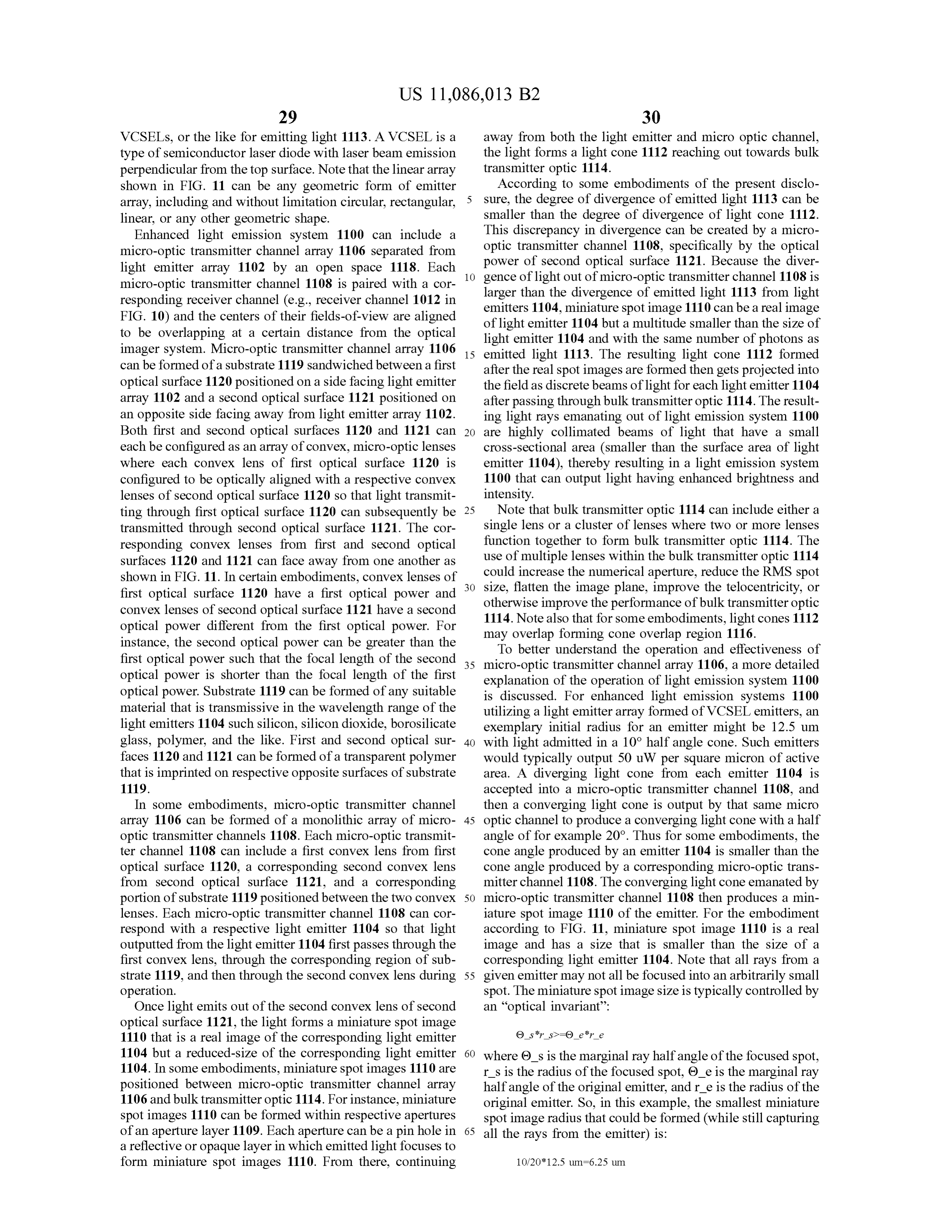
Page 56
Note that this smaller spot will have one fourth the area where each convex lens of optical surface 1220 is configured of the original emitter, and thus has a power density of 200 to be optically aligned with a respective light emitter 1204 W per square micron of spot area . Each micro -optic so that light outputted by the respective light emitter 1204 transmitter channel 1108 typically has one or more optical can transmit through the respective convex lens of optical surfaces, having characteristics that may for example and 5 surface 1220. Convex lenses from optical surface 1220 can without limitation include a focal length of 50 um , and a lens faceaway from their respective light emitters 1204 as shown diameter of 80 um . in FIG . 12 so that their focal points are positioned further For some embodiments, the distance between light emit from light emitter 1204. In certain embodiments, convex ter 1104 and a corresponding micro - optic transmitter chan lenses of optical surface 1220 have an optical power suitable nel 1108space
be forbetween exampleemitter and without array limitation 1102 and 150 um . 10 for converging the emitted light into real miniature spot micro optic transmitter channel array 1106 as shown in FIG . 11 emitters images 1210 that are real images of corresponding light may be , for example and without limitation an air gap such light emitters 1204 but reduced - size images of the corresponding as that produced by methods typically used to manufacture 1204 like the convex lenses of second optical MEMS devices . The distance between emitter array 1102 15 emitted surface 1121 in FIG. 11. Optical surface 1120 enables the light to diverge into light cones 1212 before pro and micro - optic transmitter channel array 1106 for example jecting through bulk imaging optic 1214. Substrate 1219 and
Bulk transmitter optic 1114 is positioned in front of the optical surface 1220 can be formed of similar materials as micro - optic and emitting layers such that the focal plane of substrate 1119 and optical surfaces 1120 and 1121 discussed the bulk imaging optic coincides with miniaturized spot 20 herein with respect to FIG . 11. In some embodiments, light images 1110. Bulk transmitter optic 1114 accepts divergent cones 1212 may overlap forming cone overlap region 1216 . light cone ( s ) 1112 and outputs a collimated beam . Its Embodiments herein can also implement micro -optic numeric aperture can be at least large enough to capture the channel arrays that do not include convex lenses and that do full range of angles in the divergent ray cone ( s ) , so for not generate real images of the light emitters. Rather, some example and without limitation the Numerical Aperture 25 embodiments may implement concave surfaces to generate (NA ) = 0.34 in this example. Also , bulk transmitter optic 1114 virtual images of the light emitters , as discussed further can be image - space telecentric, since light cone ( s ) 1112 herein with respect to FIG . 13 .
exiting the micro -optic layer may all be parallel (rather than FIG . 13 is a simplified cross - sectional view diagram of a having their center axes aimed towards the center of the bulk third exemplary enhanced light emission system 1300 , optic ) . In one embodiment, light can exit bulk transmitter 30 according to some embodiments of the present disclosure . optic 1114 approximately collimated . Note that the quality Similar to first and second exemplary enhanced light emis of beam collimation relates to the size of the “ emitting sion systems 1100 and 1200 , third exemplary enhanced light object ” (miniature spot images 1110 ) at the focal plane. emission system 1300 can include bulk imaging optic 1314 Since this “ emitting object ” size has been reduced by using and light emitter array 1302. However, unlike first and a micro - optic stack , a better collimation angle is obtained 35 second exemplary light emission systems 1100 and 1200 , than if the emitter object was simply imaged directly. third exemplary light emission system 1300 can include a Although FIG . 11 shows an enhanced light emission micro - optic transmitter channel array 1306 that includes an system having a micro -optic channel array formed of a array of concave surfaces instead of an array of convex substrate sandwiched between first and second optical sur- lenses , as shown in FIG . 13 .
faces, and positioned a distance away from a light emitter 40 In such embodiments , micro - optic transmitter channel array by an open space to improve the brightness and array 1306 can be formed of a substrate 1319 and an optical intensity of light outputted by the light emission system , surface 1320. Optical surface 1320 can be a first surface embodiments are not limited to such configurations. Rather, 1330 of substrate 1319 positioned toward bulk imaging optic other embodiments may not necessarily implement an open 1314 and away from light emitters 1304. Second surface space or two optical surfaces, as discussed further herein 45 1331 of substrate 1319 can be located opposite of first with respect to FIG . 12 . surface 1330 and positioned against light emitter array 1302 FIG . 12 is a simplified cross - sectional view diagram of a so that light emitted from emitters 1304 can first pass second exemplary enhanced light emission system 1200 , through substrate 1319 before passing through optical sur according to some embodiments of the present disclosure. face 1320. Optical surface 1320 can each be configured as Similar to first exemplary enhanced light emission system 50 an array of concave surfaces where each concave surface of 1100 , second exemplary enhanced light emission system optical surface 1320 is configured to be optically aligned 1200 can include bulk imaging optic 1214 and light emitter with a respective light emitter 1304 so that light outputted by array 1202. However, unlike first exemplary light emission the respective light emitter 1304 can transmit through the system 1100 , second exemplary light emission system 1200 respective concave surface of optical surface 1320. In cer can include a micro - optic transmitter channel array 1206 55 tain embodiments, the concave surfaces of optical surface that is positioned directly upon an emission surface of light 1320 have an optical power suitable for forming virtual emitter array 1202 instead of being separated by an open miniature spot images 1310 that are virtual images of space / air gap , as shown in FIG . 12 . corresponding light emitters 1304 but reduced -size images In such embodiments , micro -optic transmitter channel of the corresponding light emitters 1304 , and further enable array 1206 can be formed of a substrate 1219 and an optical 60 the emitted light to diverge into light cones 1312 before surface 1220. Optical surface 1220 can be positioned on a projecting through bulk imaging optic 1314. In some first surface 1230 of substrate 1219. Second surface 1231 of embodiments, virtual miniature spot images 1310 are substrate 1219 can be located opposite of first surface 1230 formed within substrate 1319 as shown in FIG . 13. In some and positioned against light emitter array 1202 so that light embodiments, light cones 1312 may overlap forming cone emitted from emitters 1204 can first pass through substrate 65 overlap region 1316. Substrate 1319 can be formed of 1219 before passing through optical surface 1220. Optical similar materials as substrate 1119 discussed herein with surface 1220 can be configured as an array of convex lenses respect to FIG . 11 .
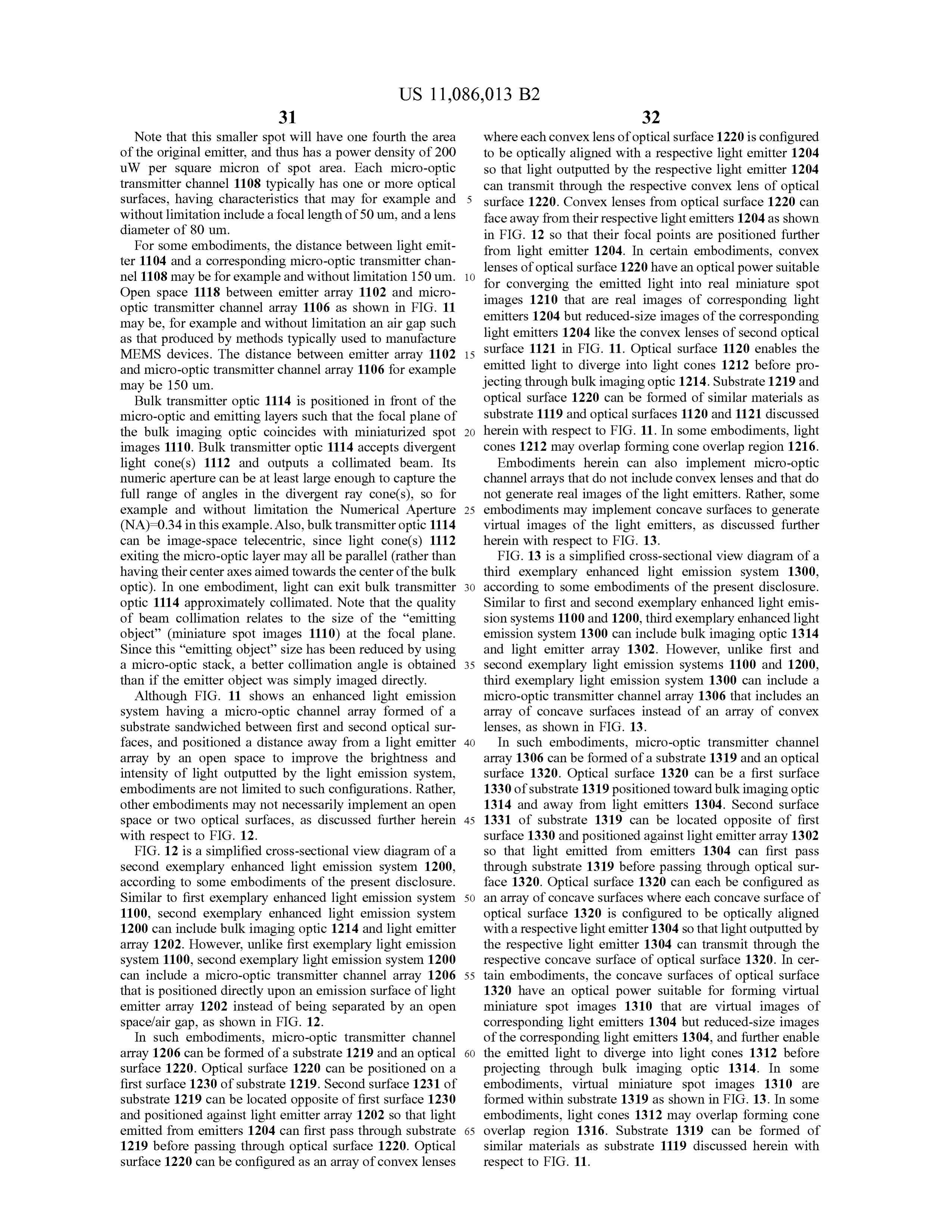
Page 57
Note that the lens configurations for the micro -optic B. Optical Corrections for Astigmatism channels for embodiments described in each of FIGS . 11 , 12 As mentioned herein with respect to FIG . 7 , light detec and 13 differs with respect to how many surfaces have tion systems and light emission systems can be enclosed optical power and the shapes of those surfaces. The first within the same protective structure, e.g. , stationary housing embodiment shown in FIG . 11 benefits from the ability to 5 702 , optically transparent window 704 , and stationary lid use two optical power surfaces on opposite sides of a 706 in in FIG . 7. Light emitted from the light emission system , some embodiments, exits out of transparent window 704 , substrate, which could allow each surface to be shallower , spherical rather than aspherical, or otherwise more easily and light detected by light detection system may first enter into transparent window 704. The curvature of transparent manufactured . This embodiment includes a spacer structure 10 window ( not shown) to maintain an offset between the micro -optic astigmatism 704 can induce some optical aberrations, such as channel array 1106 and the light emitter array 1102. An cylindrical structure . Because the transparent window can have a example of such a spacer structure would be a silicon wafer rected and be well -controlled , it can be cor with one or with channels formed via deep reactive ion etching. The some embodiments, light emission more additional optical structures. In and / or detection systems second embodiment shown in FIG . 12 benefits from having 15 can be configured with corrective optical structures to com only one optical power surface on a substrate that is attached pensate for the astigmatism caused by the transparent win to the light emitter array. This type of configuration simpli- dow , as discussed further herein . fies fabrication while also achieving enhanced brightness FIGS . 15A - 15C are cross - sectional views of simplified and intensity . The third embodiment shown in FIG . 13 diagrams of exemplary active imager systems having dif shares the benefits of the embodiment shown in FIG . 12 but 20 ferent implementations of corrective optical structures for has a single optical surface that is formed of concave astigmatism , according to some embodiments of the present surfaces rather than convex lenses ; concave features can disclosure . Specifically, FIG . 15A is a simplified cross often be easier to fabricate at the micro -scale . sectional view diagram of an active imager system 1500 In some embodiments, bulk imaging optics for light having a corrective optical structure as part of the bulk emission systems can include one or more aperture stops to 25 imaging optic , FIG . 15B is a simplified cross - sectional view reduce stray light emitted by the system . For instance , FIG . diagram of an active imager system 1501 having a corrective 14 is a simplified cross - sectional view diagram of an exem- optical structure as part of the micro - optic receiver channel plary enhanced light emission system 1400 configured with array, and FIG . 15C is a simplified cross - sectional view bulk optics that have aperture stops , according to some diagram of an active imager system 1502 having a corrective embodiments of the present disclosure . FIG . 14 is substan- 30 optical structure as part of the micro -optic transmitter chan tially similar to FIG . 1 with the addition of aperture stop nel array . Active imager systems 1500 , 1501 , and 1502 each variants 1403 , 1405 , and 1406 for bulk transmitter optic include a light detection system 1504 and a light emission 1414. Aperture stop ( s ) shown in FIG . 14 can be used with system 1506. Components of active imager systems 1500 , any of FIGS . 11 through 13. In FIG . 14 , aperture stops 1403 , 1501 , and 1502 are substantially similar to active optical 1405 , and 1407 , can have circular or oval openings for light 35 imager system 1000 in FIG . 10 with the addition of the to pass through , although any opening shape may be utilized corrective optical structures . Thus, the components that are without deviating from the spirit and scope of the present shared with active optical imager system 1000 are not disclosure . discussed for brevity.
In some embodiments, aperture stop 1403 can be located As shown in FIG . 15A , active imager system 1500 can be on a side of bulk transmitter optic 1414 facing away from 40 housed within an enclosure containing a transparent window light emitter array 1402 and micro -optic transmitter channel 1508. Transparent window 1508 is at least transparent to the array 1406. In some additional and alternative embodiments, wavelength of light at which emitters 1510 operate. The aperture stop 1405 can be located on a side of bulk trans- curved shape of transparent window 1508 can induce an mitter optic 1414 facing toward light emitter array 1402 and optical aberration, such as an astigmatism , in light rays 1511 micro - optic transmitter channel array 1406. In yet some 45 emitted from light emission system 1506 when light rays additional and alternative embodiments where bulk receiver 1511 exit the enclosure through transparent window 1508 . optic 114 includes a plurality of lenses working together, Light rays 1512 then enter back into the enclosure through aperture stop 1407 can be formed of one or more aperture transparent window 1508 after reflecting off of an object in stops placed within the plurality of lenses that form bulk the field , which can induce an additional optical aberration transmitter optic 1414 . 50 to the received light rays. To correct for these optical The various configurations and locations of aperture stops aberrations, light detection system 1504 can include correc 1403 , 1405 , and 1407 can dictate the way each aperture stop tive bulk imaging optic 1514 specifically designed to com functions in the light emitting system . For example, if all the pensate for the expected astigmatism induced by transparent light cones 1412 are compressed to be substantially over- window 1508. For example , corrective bulk imaging optic lapping near the location of aperture stop 1407 , then the size 55 1514 can include a corrective lens 1516 in addition to bulk of the aperture stop 1407 would be able control both the receiver optic 1518. Corrective lens 1516 can be any suitable initial diameter of the emitted collimated beams as well as lens capable of negating the astigmatism caused by trans reject the marginal rays emitted by light emitters 1404. parent window 1508 , such as a cylindrical lens . Corrective Rejecting certain ray angles could effectively narrow the lens 1516 can be positioned between transparent window spectrum of light emitted out of the bulk optic , since the 60 1508 and bulk receiver optic 1518 in some embodiments, or wavelength of light emitted by many types of lasers varies between bulk receiver optic 1518 and micro -optical receiver with angle. Alternatively, perhaps this best location for the channel array 1505 in some other embodiments . Similarly , a aperture stop would occur at 1402 or 1403 , depending upon corrective bulk optic could be included in the bulk trans the design of the bulk transmitter optic 1414. Multiple mitter optic of the light emission system 1506 . aperture stops may be used simultaneously -e.g . 1402 , 65 Instead of incorporating the corrective optics into the bulk 1403 , and 1404 all in one bulk transmitter optic 1414_to imaging optics , the corrective optics can be implemented reduce stray light emitted by light emitting system 1400 . into a micro -optical receiver channel array in some embodi
Page 58
ments . For instance, with reference to FIG . 15B , light light to bleed into neighboring channels, thereby resulting in detection system 1504 can include a corrective lens array inaccurate readings of reflected light for each pixel in the 1520 in front of apertures 1522 , e.g. , on the opposite side of field. Ideally, no stray light should be received by any apertures 1522 from where photosensors 1526 are posi- channel, as shown in FIG . 16A .
tioned . That way , light cones 1524 can propagate through 5 FIG . 16A is a simplified cross - sectional view diagram of respective corrective lenses to compensate for astigmatism part of a light detection system 1600 where there is no caused by transparent window 1508 before projecting on cross - talk between channels. During operation , perpendicu photosensors 1526. In some embodiments, corrective lens lar light rays 1602 and chief ray 1604 enter the bulk imaging array 1520 is formed of an array of cylindrical lenses that optic 1606 and produce light cone 1608. Light rays 1602 and can negate the astigmatism caused by transparent window 10 1604 enter an aperture of aperture layer 1610 and enter 1508. Each corrective lens of corrective lens array 1520 can collimating lens 1611. Collimating lens 1611 accepts a be positioned in alignment with a respective aperture 1522 limited range of incident light angles . For example, colli so that corrective lens array 1520 can negate the astigmatism mating lens 1611 can accept light rays at incident angles caused by transparent window 1508 for light received by between +25 to -25 degrees relative to the perpendicular. each photosensor 1526 . 15 FIG . 16A shows light cone 1608 with incident angles Although FIGS . 15A and 15B illustrate ways in which a between +25 to -25 degrees. The chief ray 1604 is the light light detection system portion of a LIDAR system can be ray that passes through the center of the aperture. In this modified to correct for astigmatism caused by transparent example , the chief ray 1604 has an incident angle of 0 window 1508 , embodiments are not limited to such con- degrees on the collimating lens 1611 .
figurations and corrective optics can be implemented in light 20 FIG . 16B is a simplified cross - sectional view diagram of emission systems as well . For example, with reference to part of a light detection system 1601 where there is cross FIG . 15C , active imager system 1502 can include a correc- talk between channels. In this case , during operation , tive lens array 1528 in front of aperture layer 1530 , e.g. , on oblique light rays 1612 and chief ray 1614 enter bulk the opposite side of aperture layer 1530 from where light receiver optic 1616 and later enter collimating lens 1621. In emitters 1510 are positioned . That way , light emitted from 25 this example, collimating lens 1621 belongs to a micro -optic light emitters 1510 can propagate through respective cor- channel that corresponds to a photosensor further from the rective lenses 1528 before emitting to bulk transmitter optics center of the image . In this example , chief ray 1614 has an 1534. In this case , respective corrective lenses 1528 can incident angle of -12 degrees and the cone of focused light induce a corrective degree of astigmatism in the emitted has incident angles between +12 degrees to -35 degrees . light in anticipation of, and to compensate for, the astigma- 30 Collimating lens 1621 rejects some of the light rays because tism caused by transparent window 1508 as light is emitted it only accepts light with incident angles between +25 to -25 out of light emission system 1506. In some embodiments, degrees. Additionally , the rays that are outside of the colli corrective lens array 1528 is formed of an array of biconical mating lens acceptance cone can travel to other optical lenses that can induce an equal but opposite degree of surfaces and become stray light. Thus, a non - telecentric bulk astigmatism caused by transparent window 1508. Thus, the 35 imaging optic will deliver significantly fewer signal photons amount of astigmatism induced by corrective lens layer to the photodetector, while potentially polluting other chan 1528 can be offset by the degree of astigmatism caused by nels with errant light rays 1622. A telecentric bulk imaging transparent window 1508 , thereby effectively achieving optic , on the other hand, will produce light cones with little to no net astigmatism during operation of active imager incident angles approximately between +25 to -25 degrees system 1502. Each corrective lens of corrective lens array 40 and chief rays with incident angles on the collimating lens 1528 can be positioned in alignment with a respective of approximately 0 degrees, regardless of the angle of the aperture 1532 so that corrective lens array 1528 can induce oblique rays 1612 and chief ray 1614. A telecentric bulk a corrective degree of astigmatism to negate the astigmatism imaging optic has similar benefits for the transmitter when caused by transparent window 1508 for light received by the lasers are telecentric (their chief rays are all parallel) as each photosensor 1526. In some embodiments, corrective 45 is the case for VCSELS or a side emitter diode laser bar. lens array 1528 may not be needed . Instead , optical surface In some embodiments, the light detection system of a light 1536 can be an array of biconical lenses instead of an array sensing module uses an input image - space telecentric bulk of cylindrical lenses. The biconical structure of the lenses imaging optic . In some other embodiments, for example can induce an amount of astigmatism to offset the degree of where cost or increased field of view is more important than astigmatism caused by transparent window 1508. In these 50 performance, the light detection system may use a more embodiments, corrective lens array 1528 may not be imple- standard input bulk imaging optic such as a bi - convex lens. mented in light emission system 1506. Furthermore , in some For any given input field into an image - space telecentric embodiments , instead of ( or in conjunction with) a correc- lens , the resulting chief rays are parallel to the optical axis, tive micro - optic lens array, a corrective bulk cylindrical lens and the image - side ray cones all span approximately the can be implemented with bulk receiver optic 1534 ( similar 55 same set of angles . This allows micro -optic channels far to the embodiment shown in FIG . 15A for light detection from the optical axis in the light detection system to achieve system 1504 ) . Thus, light emission system 1506 can include similar performance to the on - axis micro -optic channel. The a corrective bulk imaging optic in front of its bulk receiver light detection system does not need perfect image space optic 1534 to negate the astigmatism caused by transparent telecentricity for this to work, but the closer to perfect window 1508 . 60 telecentricity the better. For a micro - optic receiver optical V. Mitigating Receiver Channel Cross - Talk layer lens that can only accept +/- 25 degree light, the pref As can be appreciated by disclosures herein , channels in erence is that the input bulk imaging optic produce image the micro - optic receiver and are positioned very close to one side rays that are no greater than 25 degrees in angle for another, often times within microns of one another. This every point on the focal plane .
small spacing between each channel can invite the oppor- 65 In certain embodiments , specific light detection systems tunity for problems to arise . For instance, light propagating having wide field of view and narrowband imaging can have through bulk imaging optic can occasionally cause stray an input image - space telecentric bulk imaging optic with a
Page 59
numerical aperture (NA ) equal to 0.34 and focal length of 20 A photosensor layer 1770 including a photosensor 1771 mm . Similarly , some other embodiments could have a 1 nm adjacent to optical filter layer 1760 and configured to wide bandpass filter, thereby enabling it to detect light of a detect photons incident on photosensor 1771. Photo very specific wavelength . The light detection system is sensor 1771 herein refers to a single photodetector capable of supporting FOVs greater than 30 degrees. 5 capable of detecting photons, e.g. , an avalanche pho According to some embodiments of the present disclo todiode, a SPAD ( Single Photon Avalanche Detector), sure , the design of each channel of the micro -optic receiver RCP (Resonant Cavity Photo - diodes ), and the like , or channel array can be specifically configured to have features several photodetectors , such as an array of SPADs, that minimize the intrusion of stray light onto a respective cooperating together to act as a single photosensor, photodetector, thereby reducing or eliminating any detri- 10 often with higher dynamic range , lower dark count rate , mental effects caused by the occurrence of stray light. FIG . or other beneficial properties as compared to a single 17 is a simplified cross -sectional diagram of an exemplary large photon detection area . Each photodetector can be micro - optic receiver channel structure 1700 , also called a an active area that is capable of sensing photons , i.e. , micro - optic receiver channel in discussions herein . Receiver light. Photosensor layer 1770 refers to a layer made of channel 1700 can be representative of micro - optic receiver 15 photodetector ( s) and contains optional structures to channels 232 and 1032 , among others , shown in FIGS . 2 and improve detection efficiency and reduce cross talk with 10 , respectively, and serves to accept an input cone of light neighboring receiver structures. Photosensor layer containing a wide range of wavelengths, filters out all but a 1770 may optionally include diffusers , converging narrow band of those wavelengths centered at the operating lenses , apertures, optically non - transparent tube spacer wavelength , and allows photosensor 1771 to detect only or 20 structures, optically non - transparent conical spacer substantially only photons within the aforementioned nar- structures, etc.
row band of wavelengths. According to some embodiments Stray light may be caused by roughness of optical sur of the present disclosure, micro - optic receiver channel struc- faces, imperfections in transparent media, back reflections, tures, such as receiver channel 1700 , can include the fol- and the like , and may be generated at many features within lowing layers : 25 the receiver channel 1700 or external to receiver channel An input aperture layer 1740 including an optically trans- 1700. The stray light may be directed : through the filter parent aperture 1744 and optically non -transparent stop region 1761 along a path non -parallel to the optical axis of region 1746 configured to define a narrow field of view collimating lens 1751 ; reflecting between aperture 1744 and when placed at the focal plane of an imaging optic such collimating lens 1751 ; and generally taking any other path or as bulk receiver optic 202 or 1008 ( shown in FIGS . 2 30 trajectory possibly containing many reflections and refrac and 10 , respectively; not shown in FIG . 17) . Aperture tions . If multiple receiver channels are arrayed adjacent to layer 1740 is configured to receive the input marginal one another, this stray light in one receiver channel may be ray lines 1733. The term “ optically transparent” herein absorbed by a photosensor in another channel, thereby refers to as allowing most or all light to pass through . contaminating the timing , phase , or other information inher Light herein refers to spectrum of light in the near- 35 ent to photons . Accordingly, receiver channel 1700 may ultraviolet, visible , and near - infrared range (e.g. 300 feature several structures to reduce crosstalk between nm to 5000 nm ). Optically non - transparent herein receiver channels .
refers to as allowing little to no light to pass through, As will be understood further herein , each layer of a but rather absorbing or reflecting the light. Aperture micro - optic channel layer structure can be designed a spe layer 1740 can include optically transparent apertures 40 cific way to mitigate the detrimental effects of stray light. separated from each other by optically non - transparent Various different designs for each layer will now be dis stop regions. The apertures and stop regions can be cussed in further detail below .
built upon a single monolithic piece such as an opti- A. Aperture Layer cally transparent substrate . Aperture layer 1740 can In an embodiment having aperture layer 1740 , as shown optionally include a one - dimensional or two - dimen- 45 in FIG . 17 , optically transparent aperture 1744 and optically sional array of apertures 1744 . non - transparent stop region 1746 can be formed from a An optical lens layer 1750 including a collimating lens single monolithic piece , such as a metal foil with a pinhole 1751 characterized by a focal length , offset from the or from a single layer of a deposited opaque or reflective plane of aperture 1744 and stop region 1746 by the material having apertures etched therethrough .
focal length, aligned axially with aperture 1744 , and 50 FIG . 18A is a simplified cross - sectional view diagram of configured to collimate photons passed by the aperture a different embodiment 1800 where aperture layer 1840 has such that they are traveling approximately parallel to two apertures 1844. Both the optically transparent apertures the axis of collimating lens 1751 which is aligned with 1844 and corresponding optically non -transparent optical the optical axis of receiver channel 1700. Optical lens stop regions 1846 are supported on an optically transparent layer 1750 may optionally include apertures, optically 55 substrate 1845. Bottom aperture 1844 can be smaller and be non - transparent regions and tube structures to reduce positioned at the focal plane of the bulk optic . Aperture layer cross talk. 1840 can be followed by optically transparent spacer struc An optical filter layer 1760 including an optical filter ture 1856 positioned between aperture 1844 and collimating 1761 , typically a Bragg reflector type filter, adjacent to lens 1851 in the receiver channel. Optically transparent collimating lens 1751 and opposite of aperture 1744. 60 spacer structure 1856 forms a tube of substantially similar or Optical filter layer 1760 can be configured to pass larger diameter to collimating lens 1851 .
normally incident photons at a specific operating wave- FIG . 18B is a simplified cross - sectional view diagram of length and passband. Optical filter layer 1760 may a different embodiment 1801 of aperture layer 1840. Opti contain any number of optical filters 1761. Optical filter cally transparent aperture 1844 and optically non -transpar layer 1760 may optionally include apertures, optically 65 ent stop region 1846 are supported on optically transparent non - transparent regions and tube structures to reduce substrate 1845. Optically transparent spacer structure 1856 cross talk. that follows aperture layer 1840 and positioned between
Page 60
aperture 1844 and collimating lens 1851 forms a tube of FIG . 19C is a simplified cross - sectional view diagram of substantially similar or larger diameter to collimating lens an embodiment 1902 of aperture layer 1940 where aperture 1851 . 1944 is conically aligned , and where the conical structure as FIG . 18C is a simplified cross - sectional view diagram of an optically non -transparent layer coated on an optically an embodiment 1802 of aperture layer 1840 consisting of 5 transparent material.
multiple optically non - transparent stop regions 1846 that are FIG . 19D is a simplified cross - sectional view diagram of supported on optically transparent substrate 1845. These an embodiment 1903 of aperture layer 1940 where the layers ( stop regions 1846 ) follow the contour of marginal aperture 1944 is conically aligned, and where the conical light rays ( not shown, but similar to light rays 1733 in FIG . structure is a solid structure formed of an optically non 17 ) to reduce stray light into the receiver channel. Optically 10 transparent material. As shown in FIGS . 19C and 19D the transparent spacer structure 1856 below aperture layer 1840 optically transparent aperture 1944 and optically non -trans forms a tube of substantially similar or larger diameter to parent stop region 1946 are combined into a monolithic collimating lens 1851 . layer with a conical cavity aligned with the optical axis of FIG . 18D is a simplified cross - sectional view diagram of the receiver channel and configured to conform to the shape an embodiment 1803 of aperture layer 1840 having multiple 15 of marginal ray lines ( not shown, but similar to light rays optically non - transparent stop layers 1846 supported on 1733 in FIG. 17) .
multiple optically transparent substrate 1845. Aperture layer C. Optical Filter Layer 1840 follows the contour of marginal light rays ( not shown , FIG . 20A is a simplified cross -sectional view diagram of but similar to light rays 1733 in FIG . 17 ) to reduce stray light an embodiment 2000 of filter layer 2060 for a receiver into the receiver channel. Optically transparent spacer struc- 20 channel, according to some embodiments of the present ture 1856 below aperture layer 1840 forms a tube of sub- disclosure .
stantially similar or larger diameter to collimating lens 1851 . Optical filter layer 2060 can include a single optical filter In some other embodiments of the present disclosure , 2061 supported on an optically transparent substrate 2065 . spacer structure 1856 shown in FIGS . 18A - D , can be Optical filter layer 2060 can be placed on top of optically optically non -transparent. The optically non -transparent 25 transparent substrate 2065 or below optically transparent spacer structure in this instance could be formed by etching substrate 2065. Optical filter 2061 can be a bandpass filter a silicon or glass wafer and may be coated with an optically that blocks incident light outside of a defined set of wave non -transparent material ( e.g. black chrome). Additionally, lengths ( e.g. 945-950 nm ). However, in some other embodi the spacer structure in this instance would prevent any light ments, optical filter 2061 can be an edge pass filter or any in the spacer region from traveling outside the receiver 30 other suitable type of filter that selectively allows light channel. within a wavelength range to pass through itself . B. Spacer Structure Between Aperture Layer and Optical FIG . 20B is a simplified cross - sectional view diagram of Lens Layer an embodiment 2001 of filter layer 2060 for a receiver FIG . 19A is a simplified cross - sectional view diagram of channel, according to some embodiments of the present an embodiment 1900 of the present disclosure with an 35 disclosure. Optical filter layer 2060 can include two optical optically non -transparent spacer structure between the aper- filters 2061 sandwiching and supported by an optically ture layer and the lens layer. FIG . 19A depicts an optically transparent substrate 2065. Optical filter layer 2060 can non - transparent spacer structure 1956 positioned between contain any number of optical filters 2061 on any number of aperture 1944 and collimating lens 1951 in the receiver substrates 2065. One of the optical filters 2061 as shown in channel. Optically non -transparent spacer structure 1956 40 FIG . 20B can be a bandpass filter and can be positioned on forms a tube of substantially similar or larger diameter to either on top of or directly below optically transparent collimating lens 1951 and prevents any light from traveling substrate 2065 that blocks all of the incident light for a outside the receiver channel in the region between aperture defined set of wavelengths ( e.g. 900-945 nm and 950-995 1944 and collimating lens 1951. Optically non - transparent nm ). The other optical filter 2061 placed on the opposite side spacer structure 1956 could be formed by etching a silicon 45 of the optical substrate 2065 can be a wide spectrum or glass wafer and may be coated with an optically non- blocking filter ( except for the region covered by the band transparent material ( e.g. black chrome ). Alternatively, opti- pass filter ), for example covering 200-915 nm and 980-1600 cally non - transparent spacer structure 1956 could be a solid nm . The bandpass filter and blocking filter are designed such non - transparent structure that is fabricated from molded that there is no leakage in the transition region between the polymer or any other suitable method. FIG . 19A shows the 50 two filters . However, the filters could be two edge pass filters aperture layer having optically transparent substrate 1945 on designed to work in conjunction as a bandpass filter or any the top , followed by the optically non - transparent stop other types of filters .
region 1946 and aperture 1944 , and then by optically non- In some other embodiments of the present disclosure , the transparent spacer structure 1956 . bandpass filter and wide spectrum blocking filter are merged FIG . 19B is a simplified cross - sectional view diagram of 55 into a single optical filter 2061 and placed on either the top an embodiment 1901 of the present disclosure with an or bottom of optically clear substrate 2065 .
optically non - transparent structure between the aperture 1. Filter Layer with Apertures layer and the lens layer. FIG . 1901 depicts an optically FIG . 20C is a simplified cross -sectional view diagram of non - transparent spacer structure 1956 positioned between an embodiment 2002 of filter layer 2060 for a receiver aperture 1944 and collimating lens 1951. Optically non- 60 channel, according to some embodiments of the present transparent spacer structure 1956 forms a tube of substan- disclosure. Optical filter layer 2060 can have an additional tially similar or larger diameter to collimating lens 1951 and aperture 2049 on top and an additional aperture 2054 on the prevents any light from traveling outside of the receiver bottom of optical filter layer 2060 along with the corre channel in the region between aperture 1944 and collimating sponding optically non - transparent stop regions 2063 & lens 1951. FIG . 19B shows multiple optically non - transpar- 65 2055. Aperture 2049 defines the maximal cylinder of light ent stop regions 1946 supported on optically transparent desired to be passed into optical filter layer 2060 by optical substrate 1945 . filter 2061 , and stop region 2063 an absorb or reflect any
Page 61
incident stray light outside the diameter of aperture 2049 . etches on each side of filter substrate 2065 and selectively Aperture 2054 defines the maximal cylinder of light desired depositing metal or polymer afterwards.
to be passed out of optical filter layer 2060 and stop region FIG . 20G is a simplified cross - sectional view diagram of 2055 absorbs or reflects any incident stray light outside the an embodiment 2006 of filter layer 2060 for a receiver diameter of aperture 2054. Optical filters 2061 can be 5 channel, according to some embodiments of the present supported on an optically transparent substrate 2065 . disclosure . Optical filter layer 2060 can include two optical In some embodiments of the present disclosure , filter filters 2061 supported on optically transparent substrates layer 2060 can have a single aperture 2049 placed on the top 2065 and surrounded by an optically non- transparent tube structure 2111 , which prevents stray light in one optical filter of the optical filter layer 2060. In some additional and 10 layer 2060 from traveling into an optical filter region of an alternative embodiments of the present disclosure, filter adjacent layer 2060 can have a single aperture 2054 placed on the Howeverreceiver channel in a multi receiver channel system . , the optical filter region may contain any number bottom of optical filter layer 2060 . of optical filters 2061 on any number of substrates 2065 FIG . 20D is a simplified cross - sectional view diagram of within the optical filter layer 2060. FIG . 20G illustrates an an embodiment 2003 of filter layer 2060 for a receiver 15 additional aperture 2049 and corresponding optically non channel, according to some embodiments of the present transparent stop region 2063 positioned on top of optical disclosure . Optical filter layer 2060 can include multiple filter 2061 and supported by optically transparent substrate optically transparent substrates 2065 , and multiple optically 2065. Aperture 2049 can define the maximal cylinder of non - transparent aperture layers between them in an alter light desired to be passed into optical filter layer 2060 and nating order. FIG . 20D shows an additional aperture 2049 20 stop region 2063 can absorb or reflect any incident stray and corresponding optically non - transparent stop region light outside the diameter of aperture 2049 . 2063 positioned on top of optical filter 2061 and supported Embodiment 2006 of optical filter layer 2060 in FIG . 20G by optically transparent substrates 2065 . can have an additional aperture 2054 , and corresponding Aperture 2049 can define the maximal cylinder of light optically non -transparent stop region 2055 can be positioned desired to be passed into optical filter layer 2060 by optical 25 between optical filter layer 2060 and the photosensor layer filter 2061 , and stop region 2063 absorbs or reflects any ( not shown, but similar to photosensor layer 1770 in FIG . incident stray light outside diameter of aperture 2049. FIG . 17) . Aperture 2054 can define the maximal cylinder of light 20D shows an additional aperture 2054 and corresponding desired to be passed out of optical filter layer 2060 toward optically non - transparent stop region 2055 positioned the photosensor, and stop region 2055 can absorb or reflect between optical filter layer 2060 and a photosensor layer 30 any incident stray light outside the diameter of aperture (not shown, but similar to photosensor layer 1770 in FIG . 2054. Tube structure 2111 can be formed of a variety of 17) . materials, including but not limited to silicon , metals, poly Aperture 2054 can define the maximal cylinder of light mers , or glasses .
desired to be passed out of optical filter layer 2060 toward D. Photosensor Layer the photosensor, and stop region 2055 can absorb or reflect 35 As can be appreciated herein , various different photosen any incident stray light outside the diameter of aperture sor layer designs can be implemented in a micro -optic 2054. Collectively, these interleaved layers prevent stray receiver channel.
light in one optical filter layer 2060 from traveling into an 1. Photosensor Layer with Diffuser optical filter region of an adjacent receiver channel in a multi FIG . 21A is a simplified cross - sectional view diagram of receiver channel system . 40 an embodiment 2100 of receiver channel 2132 containing an optional diffuser 2181 located in photosensor layer 2170 2. Filter Layer with Tube Structure
FIG . 20E is a simplified cross - sectional view diagram of between optical filter 2161 and photosensor 2173 , according an embodiment 2004 of filter layer 2060 for a receiver to some embodiments of the present disclosure . Diffuser channel, according to some embodiments of the present 2181 can be configured to spread collimated photons that are disclosure . Optical filter layer 2060 can include optical filter 45 output from collimating lens 2151 and passed by optical 2061 and optically transparent substrate 2065 and be sur- filter region 2160 , across the full width of a corresponding rounded by an optically non -transparent tube structure 2111 , photosensor 2173. Photosensor 2173 may be non - square or which prevents stray light in one optical filter layer 2060 non - circular in geometry (e.g. , short and wide) in order to from traveling into an optical filter region of an adjacent extend the sensing area of photosensor 2173 to be wider or receiver channel in a multi receiver channel system . Tube 50 taller than width or height of the other components in structure 2111 can be formed of a variety of materials, receiver channel 2132 .
including but not limited to silicon, metals , polymers , or Diffuser 2181 is configured to spread light rays across the glasses . area of photosensor 2173 such that photosensor 2173 is able FIG . 20F is a simplified cross - sectional view diagram of to detect the incident photons across its full width and an embodiment 2005 of filter layer 2060 for a receiver 55 height, thereby increasing the dynamic range of receiver channel, according to some embodiments of the present channel 2132 , even where the overall height of receiver disclosure . Optical filter layer 2060 can include optical filter channel 2132 has to be limited for practical considerations . 2061 and optically transparent substrate 2065 and is sur- In particular, in this embodiment, receiver channel 2132 may rounded by an optically non -transparent tube structure 2111 , include widened photosensors exhibiting greater photode which prevents stray light in one optical filter layer 2060 60 tectors 2171 ( i.e. , areas sensitive to incident photons) and a from traveling into an optical filter region of an adjacent diffuser 2181 arranged over photosensor 2173 that spreads receiver channel in a multi receiver channel system . Tube light passed by optical filter 2161 across the full area of structure 2111 can be formed of a variety of materials, photosensor 2173 , thereby yielding increased dynamic including but not limited to silicon, metals , polymers , or range .
glasses . As shown in FIG . 20F, tube structure 2111 may only 65 In some embodiments, photosensor 2173 includes an pass partially through optical filter layer 2060. This type of array of single -photon avalanche diode detectors 2171 (here structure can be formed by performing deep anisotropic inafter “ SPADs” ). The height and width of the receiver
Page 62
channel ( usually defined by the diameter of collimating lens layer 2170 can include a converging lens set 2191 , and a set 2151 ) may accommodate only a relatively small number of of apertures 2157 , wherein each aperture 2157 is aligned ( e.g. , two ) vertically -stacked SPADs. Photosensor 2173 can with a corresponding converging lens 2191. In this variation , therefore define an aspect ratio greater than 1 : 1 , and diffuser each aperture 2157 can absorb or reflect errant light rays 2181 can spread light rays passed by the optical filter region 5 passed by the light filter or reflected by the photosensor to 2160 according to the geometry of photosensor 2173 in further reduce crosstalk between receiver channels, thereby order to accommodate a larger sensing area per photosensor. further increasing the SNR of the system . Set of apertures By incorporating more SPADs per photosensor, the dynamic 2157 and corresponding optically non - transparent stop range of the photosensor can be increased , as it less likely for regions 2159 are built on an optically transparent substrate all SPADs to be unable to detect photons ( i.e. , to be “ dead ) 10 2158 .
simultaneously. FIG . 21D is a simplified cross - sectional view diagram of In some other embodiments, photosensor 2173 includes an embodiment 2103 of photosensor layer 2170 , according an array of photodetectors 2171. The height and width of the to some embodiments of the present disclosure . Photosensor receiver channel ( usually defined by the diameter of colli- layer 2170 can include converging lens set 2191 , and set of mating lens 2151 ) may accommodate only a relatively small 15 apertures 2157 , where each aperture 2157 is aligned with a number of (e.g. , two ) vertically - stacked photodiodes . Pho- corresponding converging lens 2191. Apertures 2157 and tosensor 2173 can therefore define an aspect ratio greater corresponding optically non -transparent stop regions 2159 than 1 : 1 , and diffuser 2181 can spread light rays passed by are built on an optically transparent substrate 2158. In this the optical filter region 2160 according to the geometry of variation , apertures 2157 do not go all the way through to photosensor 2173 in order to accommodate a larger sensing 20 photodetector 2171 .
area per photosensor. By incorporating more photodiodes FIG . 21E is a simplified cross - sectional view diagram of per photosensor, the dynamic range of the photosensor can an embodiment 2104 of photosensor layer 2170 , according be increased , as it is unlikely for all photodiodes to be to some embodiments of the present disclosure . An addi saturated simultaneously. tional set of apertures 2157 and corresponding optically Receiver channel 2132 can additionally or alternatively 25 non -transparent stop regions 2159 defining desired maximal include an aperture layer interposed between optical filter light cones can be positioned between lens set 2191 and region 2160 and diffuser 2181 or between the optical filter photodetector 2171. Set of apertures 2157 and correspond region 2160 and photosensor 2173 , where aperture 2144 is ing non -transparent stop regions 2159 define a light cone for aligned with a corresponding collimating lens 2151. In this every lens in lens set 2191 and function to absorb or reflect variation , aperture 2144 can absorb or reflect errant light 30 any stray light traveling along a path not encompassed by the rays passed by the light filter or reflected by the photosensor desired light cones . The apertures may be fabricated using to further reduce crosstalk between receiver channels , standard semiconductor processes.
thereby further increasing SNR ( Signal to Noise Ratio ) of 4. Photosensor Layer with Converging Lens Set and the system . Spacer Structure Between the Lens Set and the Photosensor 2. Photosensor Layer with Converging Lens Set 35 FIG . 21F is a simplified cross - sectional view diagram of FIG . 21B is a simplified cross - sectional view diagram of an embodiment 2105 of photosensor layer 2170 , according an embodiment 2101 of receiver channel 2132 , according to to some embodiments of the present disclosure . Here, an some embodiments of the present disclosure . A photosensor optically non -transparent spacer structure 2163 is positioned layer 2170 of embodiment 2100 can include a photosensor between lens set 2191 and photosensor 2173 having photo 2173 formed of a set of discrete photodetectors 2171 ( e.g. , 40 detectors 2171 in receiver channel 2132. Optically non SPADs) and a set of inactive regions 2172 (e.g. , integrated transparent spacer structure 2163 forms a tube of substan logic ) encompassing the set of photodetectors, where each tially similar or larger diameter to a collimating lens ( e.g. , photodetector is configured to detect incident photons . Pho- collimating lens 1751 shown in FIG . 17 ) and prevents any tosensor layer 2170 can also include a converging lens set light from traveling outside of receiver channel 2132 in the 2191 interposed between optical filter region 2160 and 45 region between lens set 2191 and photosensor 2173. Opti photosensor 2173 with photodetectors 2171 , and including cally non - transparent spacer structure 2163 could be made one converging lens 2191 per discrete photodetector 2171 from optically non - transparent bulk media (e.g. silicon or within photosensor 2173 , where each lens of the converging polymer ).
lens set 2191 is configured to focus incident photons passed FIG . 21G is a simplified cross - sectional view diagram of by optical filter region 2160 onto a corresponding discrete 50 an embodiment 2106 of photosensor layer 2170 , according photodetector 2171. Each converging lens can exhibit a to some embodiments of the present disclosure . Here, opti common focal length , and converging lens set 2191 can be cally non - transparent spacer structure 2163 is positioned offset above photosensor 2173 by this common focal length between lens set 2191 and photosensor 2173 , and is made ( or by a distance substantially similar to this common focal from an optically non -transparent coating on an optically length ), and each converging lens can converge incident 55 transparent substrate (e.g. black chrome on glass ) . Optically light - collimated in optical lens layer 2150 and passed by non - transparent spacer structure 2163 forms a tube of sub optical filter region 2160 onto a corresponding photode- stantially similar or larger diameter to collimating lens 2151 tector 2171 in photosensor 2173 . and prevents any light from traveling outside of receiver In some embodiments, converging lens set 2191 inter- channel 2132 in the region between lens set 2191 and posed between optical filter region 2160 and photosensor 60 photodetector 2171 .
2173 with photodetectors 2171 employs diffracting elements 5. Photosensor Layer Spacer Structure Between the Filter in addition to or replacement of refractive elements . Layer and the Photosensor Layer 3. Photosensor Layer with Converging Lens Set and FIG . 21H is a simplified cross - sectional view diagram of Additional Apertures an embodiment 2107 of photosensor layer 2170 , according FIG . 21C is a simplified cross - sectional view diagram of 65 to some embodiments of the present disclosure . Optically an embodiment 2102 of photosensor layer 2170 , according non - transparent spacer structure 2163 can be positioned to some embodiments of the present disclosure . Photosensor between an optical filter layer (e.g. , any of the above
Page 63
mentioned optical filter layers) and photosensor layer 2170 . photo sensitive diode to improve the photon detection effi Optically non - transparent spacer structure 2163 forms a tube ciency. Each photosensor 2173 includes one or more reso of substantially similar or larger diameter to a collimating nant photo - cavity diodes. Each photosensor 2173 includes lens ( e.g. , collimating lens 1751 in FIG . 17 ) and prevents one or more photo - diodes 2174 (photodetectors) along with any light from traveling outside of the receiver channel (e.g. , 5 highly - reflective (e.g. , partially -mirrored ) surfaces facing channel 1700 in FIG . 17 ) in the region between the optical the top and bottom of the area (the resonant cavity) . Gen filter layer and photosensor layer 2170. Optically non- erally, an photodetector of a non -resonant cavity diode may transparent spacer structure 2163 can be formed by etching have a relatively low quantum efficiency. To improve the a silicon or glass wafer and may be coated with an optically percentage of photons detected by the photodetector, reso non -transparent material ( e.g. black chrome ). Alternatively, 10 nant photo - cavity diode 2174 is used that includes : a first optically non -transparent spacer structure 2163 can be fab- mirrored surface 2175 below and facing the photodetector; ricated from molded polymer. In this embodiment, lens set and a second partially mirrored surface 2176 above and 2191 is directly bonded to photosensor 2173. Similar to its facing the photodetector, that also allows light to enter the function in previous embodiments , lens set 2191 serves to cavity as shown in FIG . 21K . Thus, when a photon passes focus light onto photodetectors 2171 of photosensor 2173 , 15 through and is not detected by an photodetector of resonant rather than the inactive areas . These lenses could be inte- photo -cavity diode 2174 , first mirrored surface 2175 sur grated directly on top of an ASIC containing photosensor rounding the photodetector of resonant photo -cavity diode 2173 in a wafer fabrication process, easing production. 2174 reflects the photon back toward top reflective surface 6. Photosensor Layer with Conical Spacer Structures 2176 of the cavity and through the photodetector again , FIG . 211 is a simplified cross - sectional view diagram of 20 which may detect the photon upon its second transition an embodiment 2108 of photosensor layer 2170 , according through the photodetector. However, if the photodetector to some embodiments of the present disclosure. In this fails to detect the photon upon this second collision , the embodiment, photosensor layer 2170 includes a set of coni- reflection process is repeated with the second mirrored cal , optically non - transparent spacer structures 2164 that is surface reflecting the photon back toward the photodetector, positioned between a lens set ( not shown but , e.g. , lens set 25 which again may detect the photon upon its third collision 2191 in FIGS . 21F and 21G) and photosensor 2173. Set of with the photodetector. This process may repeat until the conical , optically non -transparent spacer structures 2164 can photon is detected by the photodetector of the photosensor form tapered tubes, each with substantially similar entrance or the photon escapes or is absorbed by the cavity. Resonant diameter to individual lenses in the lens set, and each with photo -cavity diode 2174 can thus achieve a relatively high substantially similar exit diameter to the individual photo- 30 rate of photon detection (i.e. approaching 100 % ) . Note that detectors 2171 of photosensor 2173. Set of conical , optically a particle interpretation of light is used in the preceding non - transparent spacer structures 2164 prevents any light description, but consideration of wave interference effects from traveling outside of the receiver channel in regions are critical for a complete description of resonant cavity between the lens set and photosensor 2173 and also guide photodiodes . Also note that the active region of resonant light toward the photodetectors 2171 of photosensor 2173. 35 photo -cavity diode 2174 may be comprised of a standard The set of conical, optically non - transparent spacer struc- photodiode, an avalanche photodiode, a SPAD , or any other tures 2164 can be formed by etching a silicon or glass wafer photosensor.
and may be coated with an optically non - transparent mate- FIG . 21K further shows that one or more resonant cavity rial (e.g. black chrome ). Alternatively, set of conical, opti- photodiodes (or “ RCPs ” ) 2174 may be combined with cally non - transparent spacer structures 2164 can be fabri- 40 aperture 2144 , collimating lens 2151 , optical filter region cated from molded polymer. 2160 , and any combination of the aforementioned diffusers, FIG . 21J is a simplified cross - sectional view diagram of converging lens sets, or crosstalk mitigation structures to an embodiment 2109 of photosensor layer 2173 , according form a variant of receiver channel 2132.A typical RCP will to some embodiments of the present disclosure. In this have similar wavelength sensitivity as optical filter region embodiment, photosensor layer 2173 includes a set of coni- 45 2160 and can be designed to be sensitive to a similar set of cal , optically non - transparent spacer structures 2164 that is wavelengths of light as optical filter region 2160. However, positioned between a lens set (not shown but , e.g. , lens set due to fabrication or other limitations, the RCP may have 2191 in FIGS . 21F and 21G) and photodetector 2171. The more part -to - part variability of the center wavelength of the inner walls of the set of conical , optically non - transparent RCP's operating spectrum and thus necessitate a broader spacer structures 2164 are coated with a reflective material 50 operating wavelength band in order for every photosensor to ( e.g. chrome) in order to further enhance the structures ' be capable of detecting photons at the system's operating ability to act as a light pipe . Set of conical , optically wavelength. Alternatively, it may simply be impossible to non - transparent spacer structures 2164 form tapered tubes , reliably fabricate an RCP with an operating wavelength band each with substantially similar entrance diameter to indi- as narrow as the filter passband . For instance , optical filter vidual lenses in the lens set , and each with substantially 55 region 2160 may have a passband as narrow as 0.1 nm , while similar exit diameter to the individual photodetectors 2171 the RCP may have an operating band of 10 nm . With the of photosensor 2173. Set of conical , optically non -transpar- optical filter region 2160 on top of the RCP 2174 , the ent spacer structures 2164 prevents any light from traveling combined filter and RCP system has an effective operating outside of the receiver channel in regions between the lens wavelength band substantially similar to optical filter region set and photosensor 2171 and also guide light toward the 60 2160. In addition, the RCP performance is improved when photodetectors 2171 of photosensor 2173 . sensing collimated light, as opposed to focused light, which 7. Photosensor Layer with Resonant Photo - Cavity Diodes is provided as a result of collimating lens 2151 as depicted FIG . 21K is a simplified cross - sectional view diagram of in FIG . 21K . In this way, a system employing aperture 2144 , a receiver channel 2132 including an embodiment 2110 of collimating lens 2151 , optical filter region 2160 , and RCP photosensor layer 2170 , according to some embodiments of 65 2174 may achieve high photon detection efficiency and the present disclosure. In this embodiment, photosensor narrow wavelength selectivity to maximize the SNR within layer 2170 is configured with a resonant cavity around a receiver channel 2132 .
Page 64
E. Hemispherical Receiver Structures 2267 , where the center of hemisphere 2267 is located at or FIG . 22A is a simplified cross - sectional view diagram of near the focal point of incoming light ( ray lines 2233 ) . The an embodiment 2200 of a receiver channel 2232 , according center of hemisphere 2267 also corresponds to , or nearly to some embodiments of the present disclosure . Receiver corresponds to , the center of the aperture 2244. As shown in channel 2232 of embodiment 2200 can include convex 5 FIG . 22D , hemisphere 2267 can be below aperture layer hemispheres supported on an optically non - transparent 2240. In some other embodiments , hemisphere 2267 can be material. In this embodiment, an aperture layer 2240 is above aperture layer 2240 , as shown in FIG . 22E . combined with an optical filter 2261 coated on a convex FIG . 22E is a simplified cross - sectional view diagram of hemisphere 2267 , with the center of hemisphere 2267 an embodiment 2203 of a receiver channel 2232 , according located at or near the focal point of incoming light (marginal 10 to some embodiments of the present disclosure. Unlike ray lines 2233 ) . The center of hemisphere 2267 also corre- embodiment 2202 in FIG . 22D , embodiment 2215 in FIG . sponds to , or nearly corresponds to , the center of aperture 2E can be configured so that hemisphere 2267 is positioned 2244. In some embodiments, hemisphere 2267 can be below above aperture 2244 to achieve similar functionality as aperture 2244 , as shown in FIG . 22A . An advantage of the embodiment 2202 but with a more compact footprint. embodiment is that for a sufficiently well- focused cone of 15 FIGS . 22D and 22E show convex hemisphere 2267 as rays, any ray lines 2233 will pass through optical filter 2261 being coated with optical filter 2261 and imprinted on normal to the filter's surface , thereby eliminating CWL aperture layer 2240 that is supported on a rigid optically ( Center Wave Length ) shift due to variations in incident transparent layer 2245 (e.g. glass , polymer ) with aperture angle of the light ( e.g. light rays 2233 ) on optical filter 2261 , 2244 along with the corresponding optically non - transparent thereby allowing the use of very narrow bandpass (e.g. 20 stop regions 2246. As illustrated in FIGS . 22D and 22E , 850-852 nm ) filters . receiver channel 2232 includes sidewalls 2263 between This is further illustrated in FIG . 22B , which is a simpli- optically transparent layer 2245 and photosensor layer 2270 fied cross - sectional view diagram of an embodiment 2201 of with photodetectors 2271 to reduce crosstalk . Sidewalls receiver channel 2232 , according to some embodiments of 2263 can be made up of optically non - transparent material the present disclosure . Unlike embodiment 2200 in FIG . 25 or made up of optically transparent material. In addition , 22A , embodiment 2201 in FIG . 2B can be configured so that sidewalls 2263 can also be coated with reflective or absorp hemisphere 2267 is positioned above aperture 2244 to tive material. Note that, while not shown in FIGS . 22D and achieve similar functionality but with a less compact foot- 22E , there may be refraction of rays 2233 entering and print. As shown in FIG . 22B , the angle of incidence on exiting the rigid optically transparent layer 2245 . optical filter 2261 is normal for marginal ray lines 2233 (and 30 FIG . 22F is a simplified cross - sectional view diagram of all other ray lines not shown explicitly in FIG . 22B ) that pass an embodiment 2204 of a receiver channel 2232 , according through the center of hemisphere 2267. Note that, while not to some embodiments of the present disclosure. Embodi shown in FIG . 22B or 22C , the rays will refract upon exiting ment 2204 can include a concave hemisphere 2267 made of the hemisphere structure since they are not normal to the optically transparent material (e.g. glass , polymer ) with a planar exit surface . Similarly, in FIG . 22A, there will be 35 coated optical filter 2261. Self -supported aperture layer some amount of refraction when rays enter the flat side of 2240 can overhang concave hemisphere 2267 and can be the hemispherical structure . perforated or etched with an optically non - transparent rigid As illustrated in FIGS . 22A to 22B , receiver channel 2232 material (e.g. metal film ) to form the optically non -trans includes sidewalls 2263 between optically non - transparent parent stop regions 2246. As shown in FIG . 22F, hemisphere stop region 2246 and photosensor layer 2270 with photo- 40 2267 can be positioned below aperture layer 2240. The detectors 2271 to reduce crosstalk . Sidewalls 2263 can be center of aperture 2244 can be located at or near the focal made up of optically non - transparent material or made up of point of the incoming light ( rays 2233 ). Additionally, the optically transparent material. In addition, sidewalls 2263 center of the hemisphere 2267 can be located at or near the can also be coated with reflective or absorptive material. focal point of the incoming light ( rays 2233 ) . As illustrated A close -up view of the convex hemispherical surface is 45 in FIG . 22F, receiver channel 2232 includes sidewalls 2263 shown in FIG . 22C , which is a simplified cross - sectional between optically transparent layer 2245 and photosensor view diagram of convex hemisphere 2267 of FIGS . 22A and layer 2270 with photodetectors 2271 to reduce crosstalk . 22B . Convex hemisphere 2267 can be coated with optical Sidewalls 2263 can be made up of optically non - transparent filter 2261 and positioned on a self- supporting, optically material or made up of optically transparent material. In non - transparent stop region 2246 such as metal , silicon , 50 addition , sidewalls 2263 can also be coated with reflective or polymer etc. In some embodiments where the convex hemi- absorptive material.
spherical surfaces of the micro - optic channels are used for FIG . 22G is a simplified cross - sectional view diagram of hyperspectral imagers , optical filter 2261 can be configured an embodiment 2205 of receiver channel 2232 , according to to be non -uniform . For example, optical filter 2261 can be a some embodiments of the present disclosure . Unlike graduated filter increasing gradually or in a step -wise man- 55 embodiment 2204 in FIG . 22F, embodiment 2205 in FIG . ner in one direction (e.g. , the thickness direction ) that 2G can be configured so that hemisphere 2267 is positioned different micro -optic channels have different optical filter above aperture 2244 to achieve similar functionality as layers that have different thicknesses. This allows different embodiment 2204 , but embodiment 2204 may have a more micro - optic channels to measure a different range of wave compact footprint.
lengths as discussed herein with respect to FIGS . 3A and 3B . 60 FIG . 22H is a simplified cross - sectional view diagram of FIG . 22D is a simplified cross - sectional view diagram of an embodiment 2206 of receiver channel 2232 , according to an embodiment 2202 of a receiver channel 2232 , according some embodiments of the present disclosure . Receiver chan to some embodiments of the present disclosure . Receiver nel 2232 of embodiment 2206 can include a concave hemi channel 2232 of embodiment 2202 can include convex sphere 2267 and aperture layer 2240 supported by a rigid , hemisphere 2267 supported on a rigid optically transparent 65 optically transparent layer 2245. In some embodiments , layer. In this embodiment, aperture layer 2240 is combined concave hemisphere 2267 can be below the aperture layer with optical filter 2261 and coated on convex hemisphere 2240 as shown in FIG . 22H . Concave hemisphere 267 can
Page 65
be made of optically transparent material ( e.g. glass , poly- photodetectors 2371. As shown in FIG . 23E , the BMLL can mer) with a coated optical filter 2261. Aperture layer 2240 be formed of a single micro - lens 2391 for guiding divergent with optically transparent aperture 2244 and corresponding light to photodetector 2371 .
optically non - transparent stop regions 244 is supported by Embodiments 2302 and 2303 in FIGS . 23D and 23E each optically transparent layer 2245 on both top and bottom 5 include a convex hemisphere 2367 supported on a rigid sides of aperture layer 2240. The center of aperture 2244 is optically transparent layer 2345. In these illustrations, an located at or near the focal point of the incoming light ( rays aperture layer 2340 is combined with an optical filter 2361 coated on hemisphere 2367 , where the center of hemisphere 2233 ) . Additionally, the center of concave hemisphere 2267 2367 is located at or near the focal point of the incoming light is located at or near the focal point of incoming light ( rays 2233 ) . 10 (marginal ray lines 2333 ) . The center of hemisphere 2367 can also correspond to , or nearly correspond to , the center of
As illustrated in FIG . 22H , receiver channel 2232 includes aperture sidewalls 2263 between optically transparent layer 2245 and optical filter 2344. Convex hemisphere 2367 can be coated with photosensor layer 2270 with photodetectors 2271 to reduce is supported 2361 and imprinted on aperture layer 2340 that on rigid optically transparent layer 2345 ( e.g.
crosstalk . Sidewalls 2263 can be made up of optically layer formed of glass , polymer) and the corresponding non - transparent material or made up of optically transparent 15 optically non - transparent stop regions 2346. As illustrated in material. In addition, sidewalls 2263 can also be coated with FIGS . 23D and 23E , receiver channel 2332 includes side reflective or absorptive material. walls 2363 between optically transparent layer 2345 and FIG . 221 is a simplified cross - sectional view diagram of photosensor layer 2370 to reduce crosstalk . Sidewalls 2363 an embodiment 2207 of receiver channel 2232 , according to 20 can be made up of optically non - transparent material or some embodiments of the present disclosure . Unlike made up of optically transparent material. In addition , embodiment 2206 in FIG . 22H , embodiment 2207 in FIG . sidewalls 2363 can also be coated with reflective or absorp 21 can be configured so that hemisphere 2267 is positioned tive material.
above aperture 2244 to achieve similar functionality as 25 G. Additional Exemplary Receiver Channels embodiment 2206 . It is to be appreciated that a receiver channel is a structure F. Bottom Micro - Lens Layer at the micro - optic level, e.g. , a micro -optic receiver channel FIG . 23A is a simplified cross - sectional view diagram of discussed above , that can be formed from multiple layers an embodiment 2300 of a receiver channel 2332 , according including one or more of an aperture layer, an optical lens to some embodiments of the present disclosure . Receiver layer below the aperture layer, an optical filter layer below channel 2332 of embodiment 2300 can include a Bottom 30 the aperture and optical lens layer, and a photosensor layer Micro -Lens Layer ( BMLL ) , which consists of one or more below all the other layers. Each such layer can be configured micro - lenses 2391 that are configured to guide divergent in various ways to mitigate cross -talk . i.e. , exposing stray light rays into active portion of the photosensors. The BMLL light to adjacent receiver channels, as discussed herein with performs ray angle correction to guide light from dissimilar respect to FIGS . 17-23E . Various examples of receiver angles into evenly spaced photosensors . Ray angle correc- 35 channels are discussed above with respect to FIGS . 17 , tion can be achieved by controlling the lateral offset between 22A - 221 , and 23A - 23E . Two other examples of receiver lens center and the photosensor center, tilting of the lens , or channels according to the present disclosure are illustrated in adjusting the form of the lens . A better illustration of this FIGS . 24 and 25. Embodiments of the present disclosure are operation can be seen in FIG . 23B . not limited to the particular receiver channels described FIG . 23B is a simplified cross - sectional view diagram of 40 herein . Instead, based on the present disclosure a person of a close -up view of the propagation of light during ray angle skill in the art will appreciate that in other embodiments a correction by a BMLL , according to some embodiments of receiver channel according to the disclosure can include , the present disclosure . As illustrated , the pitch of the micro- among other options , an aperture layer as described above optics is either not constant or is not equal to the pitch of with respect to any of FIG . 18A - 18D or 19A - 19D , a filter lenses 2391 in order to steer the divergent rays (2333 ) to 45 layer as described above with respect to any of FIGS . active portions of photodetectors 2371 in the photosensor 20A - 20G , and / or a photosensor layer as described above layer. With reference back to FIG . 23A , each micro - lens with respect to any of FIGS . 21A - 21K . 2391 can be positioned to correspond with a respective FIG . 24 is a simplified cross - sectional view diagram of an photodetector 2371 . exemplary embodiment of a receiver channel 2400 , accord FIG . 23C is a simplified cross - sectional view diagram of 50 ing to some embodiments of the present disclosure . Receiver an embodiment 2301 of a receiver channel 2332 , according channel 2400 can include an aperture layer 2440 composed to some embodiments of the present disclosure . Receiver of first and second apertures 2444 , each formed in respective channel 2332 of embodiment 2301 can include a single optically non - transparent layers 2446a and 2446b . First micro - lens 2391 , instead of a plurality of micro - lenses as and / or second apertures 2444 can be formed of void space shown in FIG . 23A . Single micro - lens 2391 can be posi- 55 defined by openings within layers 2446a and 2446b in some tioned over and centered to a single photodetector 2371 . embodiments , while first and /or second apertures 2444 can Micro - lens 2391 can be configured to guide light to single be formed by optically transparent materials in some other photodetector 2371 embodiments. First and second optically non - transparent FIGS . 23D and 23E is a simplified cross - sectional view layers 2446a and 2446b can be supported by an optically diagram of embodiments 2302 and 2303 , respectively, of a 60 transparent substrate 2445 sandwiched between first and receiver channel 2332 , according to some embodiments of second optically non -transparent layers 2446a and 2446b . the present disclosure . Receiver channel 2332 of embodi- Receiver channel 2400 can also include an optical lens ment 2302 can include a BMLL positioned on the underside layer 2450 disposed below aperture layer 2440. Optical lens of an optically transparent layer 2345 supporting aperture layer 2450 can include a collimating lens 2451 and an layer 2340 and hemisphere 2367 with optical filter 2361 65 optically non -transparent spacer structure 2456. Collimating coated . As shown in FIG . 23D , the BMLL can be formed of lens 2451 can be separated from aperture layer 2440 by multiple lenses 2393 for guiding divergent light to multiple optically non -transparent spacer structure 2456. In some
Page 66
embodiments, optically non -transparent spacer structure layer 2540 and optical lens layer 2550. Aperture layer 2540 , 2456 forms a tube having a circumference that surrounds optical lens layer 2550 , and optical filter layer 2560 can have collimating lens 2451 and extends toward aperture layer the same construction and function as corresponding com 2440. Optically non -transparent spacer structure 2456 can ponents in FIG . 24 .
be formed of an optically reflective or absorptive material 5 Receiver channel 2500 can also include a photosensor that prevents any light from traveling outside of receiver layer 2570 positioned immediately below optical filter layer channel 2400 in the region between aperture layer 2440 and 2560. In some embodiments, photosensor layer 2570 of collimating lens 2451 . embodiment 2400 can include an optically non -transparent In addition to aperture layer 2440 and optical lens layer spacer structure 2563 , a converging lens set 2591 , and a 2450 , receiver channel 2400 can further include an optical 10 photosensor 2573. Unlike converging lens set 2491 of filter layer 2460 positioned directly below optical lens layer receiver channel 2400 in FIG . 24 , converging lens set 2591 2450. Optical filter layer 2460 can include two optical filters of receiver channel 2500 can be positioned directly on at top 2461 sandwiching an optically transparent substrate 2465 surface of photosensor 2573 instead of directly on an that structurally supports optical filters 2461. Optical filter underside of optical filter layer 2560. Furthermore , optically layer 2460 can contain any number and type of optical filters 15 non - transparent spacer structure 2563 can be formed of an 2461 on any number of substrates 2065. For instance, one of optically non -transparent material ( e.g. , black chrome) optical filters 2461 can be a bandpass filter and be positioned coated on an optically transparent layer, such as a silicon or on either on top of or directly below optically transparent glass substrate, instead of being a solid optically non substrate 2465 that blocks all of the incident light for a transparent structure , e.g. , optically non - transparent spacer defined set of wavelengths ( e.g. 900-945 nm and 950-995 20 structure 2463 of receiver channel 2400 in FIG . 24. Lens set nm ). The other optical filter 2461 placed on the opposite side 2591 serves to focus light onto photodetectors 2571 of of optically transparent substrate 2465 can be a different photosensor 2573 , rather than inactive areas 2572 . filter, such as a wide spectrum blocking filter ( except for the By implementing a receiver channel according to any of region covered by the bandpass filter ), for example covering embodiments 2400 and 2500 , errant light can be prevented 200-915 nm and 980-1600 nm . The bandpass filter and 25 from exposing on adjacent receiver channels, thereby blocking filter are designed such that there is no leakage in improving the accuracy of each photosensor's ability to the transition region between the two filters. However, the capture photons for imaging.
filters could be two edge pass filters designed to work in VI . Micro Optical Receiver Channel Array Variations conjunction as a bandpass filter or any other type of filter. According to some embodiments of the present disclo Immediately below optical filter layer 2460 can be a 30 sure , micro - optical receiver channels can be organized in an photosensor layer 2470. In some embodiments, photosensor array. The array can have various dimensions according to layer 2470 of embodiment 2400 can include an optically design . For instance, an array of micro -optical receiver non - transparent spacer structure 2463 positioned between a channels can be arranged in a MxN array where Mand N are converging lens set 2491 and a photosensor 2473. Photo- equal to or greater than 1. Accordingly, micro -optical sensor 2473 can be formed of a set of discrete photodetectors 35 receiver channels can be one- and two - dimensional arrays, 2471 ( e.g. , SPADs) positioned between a set of inactive as will be discussed furthered herein with respect to FIGS . regions 2172 ( e.g. , integrated logic ) in an alternating 26-30 , which illustrate different embodiments of micro arrangement, where each discrete photodetector is config- optical receiver channel arrays where each dot represents a ured to detect incident photons . Converging lens set 2491 micro - optical receiver channel. As aforementioned herein , can be interposed between optical filter layer 2460 and 40 each receiver channel can include a plurality of layers photosensor 2473 with photodetectors 2471 , and including stacked upon each other. Thus, it can be appreciated that one converging lens 2491 per discrete photodetector 2471 when arranged in an array, each micro - optic receiver chan within photosensor 2173 , where each lens of the converging nel is part of a monolithic layer composed of the individual lens set 2491 is configured to focus incident photons passed elements reproduced many times in the MxN arrangement, by optical filter layer 2460 onto a corresponding discrete 45 e.g. , an MxN aperture layer array , an MxN micro lens layer photodetector 2471. Each converging lens can exhibit a array , and an MxN photosensor layer array . When bonded common focal length , and converging lens set 2491 can be together, these array layers create a monolithic multi -chan offset above the sensing plane of the photosensor by this nel micro optical receiver array .
common focal length ( or by a distance substantially similar FIG . 26 is a simplified illustration of an exemplary to this common focal length ), and each converging lens can 50 micro - optical receiver array 2600 , according to some converge incident light - collimated in optical lens layer embodiments of the present disclosure . Micro -optical 2450 and passed by optical filter layer 2460 onto one receiver array 2600 is configured as a linear (Mx1 ) array , corresponding photodetector 2471 in photosensor 2473 . specifically a 16xl array . This layout can achieve a high Optically non - transparent spacer structure 2463 forms a tube resolution (e.g. 16x1024 ) as the implementation is amenable of substantially similar or larger diameter to a collimating 55 to scanning the array in one dimension.As an example, for lens 2451 and prevents any light from traveling outside of a receiver channel pitch of 500 microns the layout illustrated receiver channel 2400 in the region between lens set 2491 can be implemented in a chip of a size that is approximately and photosensor 2473. Optically non - transparent spacer 500 microns by 8000 microns .
structure 2163 could be made from optically non - transparent FIG . 27 is a simplified illustration of an exemplary bulk media (e.g. silicon or polymer ). 60 micro - optical receiver array 2700 , according to some Another exemplary embodiment of a receiver channel is embodiments of the present disclosure . Micro -optical shown in FIG . 25. FIG . 25 is a simplified cross - sectional receiver array 2700 is configured as a rectangular ( MXN) view diagram of an exemplary receiver channel 2500 , array, specifically a 16x32 array . Thus, for a receiver channel according to some embodiments of the present disclosure. pitch of 500 microns the layout illustrated can be imple Receiver channel 2500 can include an aperture layer 2540 , 65 mented in a chip of size 8,000 microns by 12000 microns . an optical lens layer 2550 disposed below aperture layer FIG . 28 is a simplified illustration of an exemplary 2540 , and an optical filter layer 2560 below both aperture micro - optical receiver array 2800 , according to some
Page 67
embodiments of the present disclosure. Micro -optical sensors , with the aperture for each channel defining a receiver array 2800 is configured as an MxN staggered discrete , non -overlapping field of view for its respec array . In this illustration , receiver channels 2832 are laid out tive channel.
in a 16x4 staggered array. This layout can achieve a high 2. The optical system for performing distance measure resolution (e.g. 64x1024 ) as the implementation is amenable 5 ments set forth in claim 1 wherein , for each receiver channel to sweeping. For a receiver channel pitch of 500 microns the in the plurality of receiver channels, there is a one - to - one layout illustrated in FIG . 28 can be implemented in a chip of correspondence between the plurality of photodetectors and a size that is approximately 2000 microns by 8375 microns . the second plurality of lenses in the photosensor for that FIG . 29 is a simplified illustration of an exemplary channel, and wherein each of the lenses in the second micro - optical receiver array 2900 , according to some 10 plurality of lenses is configured to focus photons on its embodiments of the present disclosure . Micro -optical corresponding lens in the second plurality of lenses. receiver array 2900 is configured as a warped linear (Mx1 ) array . In this embodiment, the spacing between receiver ments set forth insystem 3. The optical for performing distance measure claim 2 wherein each lens in the second channels 2932 is uneven . Receiver channels near the center, shown as 2932-01 , are placed close together (e.g. 400 15 plurality of.lenses is a converging lens having a common focal length microns apart ), while the exterior channels , shown as 2932 02 , are placed farther apart ( e.g. , greater than 400 microns 4. The optical system for performing distance measure apart ), or vice versa . This layout has an advantage of being ments set forth in claim 3 wherein each lens in the second able to allow for correction of the distortion curve of a lens plurality of lenses is spaced apart from its respective pho ( i.e. the angles between the receiver channel fields of view 20 todetector by the common focal length . are evenly spaced in the object space) . The arrangement 5. The optical system for performing distance measure shown in FIG . 29 can be used to achieve a high resolution ments set forth in claim 1 wherein the optical filter layer is ( e.g. 16x1024 ) as the implementation is amenable to sweep- disposed between the first lens layer and the photosensor ing . For an average receiver channel pitch of 500 microns layer and the first lens layer is disposed between the aperture the layout illustrated can be implemented in a chip of a size 25 layer and the filter layer.
that is approximately 500 microns by 8000 microns . 6. The optical system for performing distance measure In some embodiments, the receiver channels can be ments set forth in claim 1 wherein for each receiver channel configured in a MxN warped array (where N 1) . In such in the plurality of receiver channels, the optical filter com embodiments, the receiver channels in the center are placed further from each other in both the x and y direction than the 30 prises a first bandpass filter and a second wide spectrum exterior receiver channels . This corrects for another possible transition filter blocking region that are configured to prevent leakage in a between the two filters .
form of lens distortion .
FIG . 29 is a simplified illustration of an exemplary ments 7. The optical system for performing distance measure micro - optical receiver array 2900 , according to some source setcomprising forth in claim 1 further comprising an illumination a plurality of light emitters aligned to embodiments of the present disclosure . Micro -optical 35 project discrete beams of light into a field ahead of the receiver array 2900 is configured in an arbitrary pattern. This optical system layout arrangement has the advantage of being able to accommodate lens distortion, to make adjustments to com 8. The optical system for performing distance measure pensate for any timing or routing variations, and also to ments set forth in claim 1 wherein the lens for each receiver match an arbitrary pattern from an illumination source . 40 channel is configured to collimate light rays received Although the present disclosure has been described with through its corresponding aperture and to pass the colli respect to specific embodiments, it will be appreciated that mated light rays into its corresponding photosensor. the present disclosure is intended to cover all modifications 9. The optical system for performing distance measure and equivalents within the scope of the following claims . ments set forth in claim 1 wherein the lens for each receiver What is claimed is : 45 channel is a hemispherical substrate and the optical filter for 1. An optical system for performing distance measure- each receiver channel is a filter layer on a curved surface of ments, the optical system comprising: the lens.
a bulk receiver optic ; 10. The optical system for performing distance measure an aperture layer including a plurality of apertures ments set forth in claim 1 wherein a sensing area of each arranged along a focal plane of the bulk receiver optic ; 50 photosensor in the plurality of receiver channels is larger a first lens layer including a first plurality of lenses ; than an area of its corresponding aperture in the plurality of an optical filter layer configured to receive light after it apertures.
passes through the bulk receiver optic and pass a band 11. The optical system for performing distance measure of radiation while blocking radiation outside the band; ments set forth in claim 10 wherein the sensing area of each and 55 photosensor in the plurality of photosensors comprises a a photosensor layer including a plurality of photosensors , plurality of single photon avalanche diodes (SPADs ). wherein each photosensor includes a plurality of pho- 12. The optical system for performing distance measure todetectors configured to detect photons , and a second ments set forth in claim 11 further comprising an illumina plurality of lenses configured to focus incident photons tion source including a plurality of light emitters aligned to received at the photosensor on the plurality of photo- 60 project a plurality of discrete non -overlapping beams of light detectors ; into a field ahead of the optical system , wherein each of the wherein the optical system comprises a plurality of discrete beams of light corresponds to a field - of - view of one receiver channels with each receiver channel in the of the receiver channels .
plurality of receiver channels including an aperture 13. The optical system for performing distance measure from the plurality of apertures, a lens from the plurality 65 ments set forth in claim 12 wherein each light emitter in the of first lenses, an optical filter from the optical filter plurality of light emitters comprises a vertical cavity surface layer, and a photosensor from the plurality of photo- emitting laser (VCSEL ) .
Page 68
14. An optical system for performing distance measure- includes an optical spacer positioned between the aperture ments, the optical system comprising : and the lens from the first plurality of lenses in the receiver a bulk receiver optic ; channel.
an aperture layer including a plurality of apertures; 17. The optical system for performing distance measure a first lens layer including a first plurality of lenses ; 5 ments set forth in claim 16 wherein , for each receiver an optical filter layer configured to receive light after it channel in the plurality of receiver channels, the optical passes through the bulk receiver optic and pass a band spacer comprises a tube of substantially similar diameter to of radiation while blocking radiation outside the band; the lens.
18. The optical system for performing distance measure a photosensor layer including a plurality of photosensors , ments set forth in claim 17 wherein , for each receiver wherein each photosensor includes a plurality of pho- channel in the plurality of receiver channels, the optical todetectors configured to detect photons , and a second spacer includes walls comprising an optically non -transpar plurality of lenses configured to focus incident photons ent material.
received at the photosensor on the plurality of photo- 15 19. An optical system for performing distance measure detectors ; ments, the optical system comprising:
wherein the optical system comprises a plurality of a light emission system comprising: receiver channels with each receiver channel in the a bulk transmitter optic ;
plurality of receiver channels including an aperture an illumination source comprising a plurality of light from the plurality of apertures, a lens from the plurality 20 emitters aligned to project discrete beams of light of first lenses , an optical filter from the optical filter through the bulk transmitter optic into a field ahead layer, and a photosensor from the plurality of photo of the optical system ; and sensors , with the aperture for each channel defining a a light detection system comprising: discrete, non -overlapping field of view for its respec 25 a bulk receiver optic ;
tive channel; and an aperture layer including a plurality of apertures; wherein for each receiver channel in the plurality of a first lens layer including a first plurality of lenses ; receiver channels, the photosensor includes an optically an optical filter layer configured to receive light after it non - transparent spacer positioned between the second passes through the bulk receiver optic and pass a plurality of lenses and the plurality of photodetectors in 30 band of radiation while blocking radiation outside the photosensor. the band ;
15. An optical system for performing distance measure photosensor layer including a plurality of photosen ments, the optical system comprising : sors , wherein each photosensor includes a plurality a bulk receiver optic ; of photodetectors configured to detect photons, and an aperture layer including a plurality of apertures; 35 a second plurality of lenses configured to focus a first lens layer including a first plurality of lenses ; incident photons received at the photosensor on the an optical filter layer configured to receive light after it plurality of photodetectors; passes through the bulk receiver optic and pass a band wherein the optical system comprises a plurality of of radiation while blocking radiation outside the band; receiver channels with each receiver channel in the and 40 plurality of receiver channels including an aperture a photosensor layer including a plurality of photosensors , from the plurality of apertures, a lens from the wherein each photosensor includes a plurality of pho plurality of first lenses , an optical filter from the todetectors configured to detect photons , and a second optical filter layer, and a photosensor from the plu plurality of lenses configured to focus incident photons rality of photosensors, with the aperture for each received at the photosensor on the plurality of photo- 45 channel defining a discrete, non -overlapping field of detectors ; view for its respective channel. wherein the optical system comprises a plurality of 20. The optical system for performing distance measure receiver channels with each receiver channel in the ments set forth in claim 19 wherein , for each receiver plurality of receiver channels including an aperture channel in the plurality of receiver channels, there is a from the plurality of apertures, a lens from the plurality 50 one - to -one correspondence between the plurality of photo of first lenses, an optical filter from the optical filter detectors and the second plurality of lenses in the photo layer, and a photosensor from the plurality of photo- sensor for that channel, and wherein each of the lenses in the sensors , with the aperture for each channel defining a second plurality of lenses is configured to focus photons on discrete , non -overlapping field of view for its respec- its corresponding lens in the second plurality of lenses . tive channel; and 55 21. The optical system for performing distance measure wherein for each receiver channel in the plurality of ments set forth in claim 20 wherein each lens in the second receiver channels, the aperture layer includes an opti- plurality of lenses is a converging lens having a common cally transparent substrate disposed between first and focal length .
second optically non - transparent layers, the first opti- 22. The optical system for performing distance measure cally non - transparent layer having a first aperture with 60 ments set forth in claim 19 wherein a sensing area of each a first diameter, the second optically non - transparent photosensor in the plurality of receiver channels is larger layer having a second aperture aligned with the first than an area of its corresponding aperture in the plurality of aperture and having a second diameter different than apertures.
the first diameter. 23. The optical system for performing distance measure 16. The optical system for performing distance measure- 65 ments set forth in claim 22 wherein the sensing area each ments set forth in claim 15 wherein , for each receiver photosensor in the plurality of photosensors comprises a channel in the plurality of receiver channels, the lens layer plurality of SPADs.
Page 69
24. The optical system for performing distance measure- 28. The optical system for performing distance measure ments set forth in claim 19 wherein the plurality of apertures ments set forth in claim 25 wherein the plurality of apertures in the aperture layer are arranged along a focal plane of the in the aperture layer are arranged along a focal plane of the bulk receiver optic. bulk receiver optic.
25. An optical system for performing distance measure- 5 29. The optical system for performing distance measure ments , the optical system comprising: ments set forth in claim 25 wherein a sensing area of each a stationary housing having an optically transparent win photosensor in the plurality of receiver channels is larger dow ; than an area of its corresponding aperture in the plurality of a light ranging device disposed within the housing and 10 apertures .
aligned with the optically transparent window, the light ments , theoptical
optical system for performing distance measure system comprising:
ranging device comprising: a bulk receiver optic positioned to receive light from a a platform ; field outside of the system ;
an optical transmitter coupled to the platform , the an optical assembly disposed behind the bulk receiver optical transmitter comprising a bulk transmitter 15 optic and including a plurality of receiver channels, the optic and a plurality of transmitter channels, each optical assembly comprising:
transmitter channel including a light emitter config an aperture layer including a plurality of apertures ured to generate and transmit a narrowband light defining a plurality of non -overlapping fields of through the bulk transmitter optic into a field exter view ;
nal to the optical system ; and 20 a top lens layer including a plurality of collimating an optical receiver coupled to the platform , the optical lenses ;
receiver comprising: a bottom lens layer including a plurality of lens arrays , a bulk receiver optic ; each lens array in the plurality of lens arrays includ an aperture layer including a plurality of apertures ; ing a plurality of bottom lenses ; a first lens layer including a first plurality of lenses; 25 an optical filter layer ; and an optical filter layer configured to receive light after a plurality of pixels disposed behind the bottom lens it passes through the bulk receiver optic and pass layer, each pixel in the plurality of pixels including a band of radiation while blocking radiation out a plurality of photodetectors ; side the band ; and wherein each receiver channel in the plurality of a photosensor layer including a plurality of photo 30 receiver channels includes an aperture from the sensors , wherein each photosensor includes a plu plurality of apertures that defines a field of view for rality of photodetectors configured to detect pho the receiver channel, a collimating lens from the tons , and a second plurality of lenses configured to plurality of collimating lenses that collimates light focus incident photons received at the photosensor 35 rays received through the aperture and passes the on the plurality of photodetectors; collimated light rays to the bottom lens layer, a lens wherein the optical system comprises a plurality of array from the plurality of lens arrays in the bottom receiver channels with each receiver channel in lens layer, a pixel from the plurality of pixels , and a filter element from the optical filter layer configured the plurality of receiver channels including an to allow a band of radiation to pass through the aperture from the plurality of apertures, a lens 40 receiver channel while preventing radiation from from the plurality of first lenses, an optical filter outside the band from reaching the pixel in the from the optical filter layer, and a photosensor receiver channel; and from the plurality of photosensors , with the aper- wherein , for each receiver channel in the plurality of ture for each channel defining a discrete , non receiver channels, each bottom lens in the lens array overlapping field of view for its respective chan- 45 in the receiver channel corresponds to and is in an nel; optical path of one of the photodetectors in the a motor disposed within the housing and operatively plurality of photodetectors of the pixel in the receiver coupled to spin the light ranging device including the channel.
platform , optical transmitter, and optical receiver 31. The optical system set forth in claim 30 wherein the within the housing ; and 50 aperture layer is supported by a transparent substrate included in the optical assembly between the aperture layer a system controller disposed within the housing, the and the top lens layer.
system controller configured to control the motor and to 32. The optical system set forth in claim 31 wherein each start and stop light detection operations of the light receiver channel further comprises a first optically non ranging device . 55 transparent tubular spacing structure surrounding an optical 26. The optical system for performing distance measure surface of the collimating lens in the receiver channel. ments set forth in claim 25 wherein , for each receiver 33. The optical system set forth in claim 32 wherein each channel in the plurality of receiver channels, there is a receiver channel further comprises a second optically non one - to - one correspondence between the plurality of photo transparent tubular spacing structure surrounding optical detectors and the second plurality of lenses in the photo- 60 surfaces of the lens array in the receiver channel. sensor for that channel, and wherein each of the lenses in the 34. The optical system set forth in claim 33 wherein the second plurality of lenses is configured to focus photons on first and second optically non - transparent tubular structures its corresponding lens in the second plurality of lenses . comprise silicon .
27. The optical system for performing distance measure- 35. The optical system set forth in claim 31 wherein the ments set forth in claim 26 wherein each lens in the second 65 plurality of pixels are formed on an application specific plurality of lenses is a converging lens having a common integrated circuit (ASIC ) and the bottom lens layer is formed focal length. directly over the monolithic ASIC .
Page 70
36. The optical system set forth in claim 35 wherein , for each receiver channel, the plurality of photodetectors in the pixel for the receiver channel are separated from each other by inactive regions of the pixel and each lens in the bottom lens layer is configured to guide divergent light rays away 5 from the inactive regions into its corresponding photodetec tor.
37. The optical system set forth in claim 35 wherein the optical assembly is a monolithic structure in which the aperture layer, the top lens layer, the optical filter layer and 10 the bottom lens layer are bonded together with the ASIC . 38. The optical system for performing distance measure ments set forth in claim 30 wherein the plurality of apertures in the aperture layer are arranged along a focal plane of the bulk receiver optic . 15
Provenance
- Collection
- Patents citing this work
- Original assignee
- Ouster Inc
- Current assignee
- Sense Photonics Inc
- Pages
- 70
- Method
- pdftotext (the PDF's own text layer) + pdftoppm 300dpi page scans
- Patent office record
- patents.google.com →
- Source
- Google Patents citing-documents table
- Inventors
- Angus Pacala; Mark Frichtl; Ouster Inc
- Published
- 2021-08-10
- Transcribed from
- patentimages.storage.googleapis.com →