patent · US5982552
Planar microlens array having high converging efficiency
9 November 1999
Page 1 — bibliographic record
United States Patent (19) 11 Patent Number: 5,982,552 Nakama et al. (45) Date of Patent: Nov. 9, 1999
54) PLANAR MICROLENS ARRAY HAVING 5,359,440 10/1994 Hamada et al. .......................... 359/41 HIGH CONVERGING EFFICIENCY 5,381,187 1/1995 Takamatsu et al.. 75 Inventors: Kenichi Nakama; Satoshi Taniguchi; FOREIGN PATENT DOCUMENTS Kenjiro Hamanaka, Hiroshi Hamada, all of Osaka, Japan
European Patoff.
73 Assignees: Nippon Sheet Glass Co., Ltd; Sharp
Kabushiki Kaisha, both of Osaka, Primary Examiner-Georgia Epps p Assistant Examiner Ricky Mack
Attorney, Agent, or Firm-Ratner & Prestia
O O A microlens array of high converging efficiency is provided,
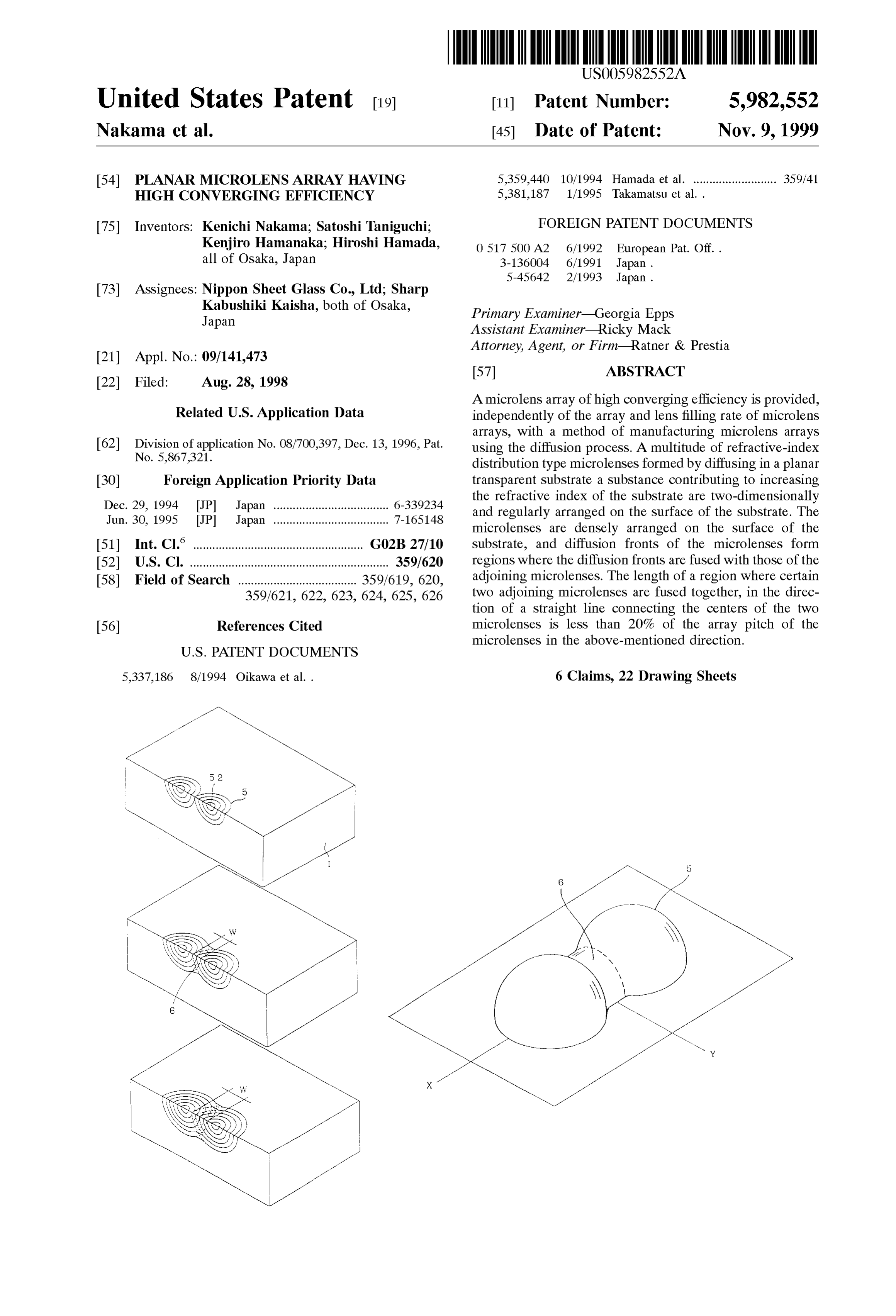
Related U.S. Application Data independently of the array and lens filling rate of microlens - - - arrays, with a method of manufacturing microlens arrayS 62 Division of application No. 08/700,397, Dec. 13, 1996, Pat. using the diffusion process. A multitude of refractive-index No. 5,867,321. distribution type microlenses formed by diffusing in a planar 30 Foreign Application Priority Data transparent Substrate a Substance contributing to increasing Dec. 29, 1994 JP J 6-339234 the refractive index of the substrate are two-dimensionally ec. 29, JP Japan .................................... and regularly arranged on the Surface of the Substrate. The Jun. 30, 1995 JP Japan .................................... 7-165148 microlenses are densely arranged on the Surface of the (51) Int. Cl." ..................................................... GO2B 27/10 Substrate, and diffusion fronts of the microlenses form 52 U.S. Cl. .............................................................. 359/620 regions where the diffusion fronts are fused with those of the 58 Field of Search ..................................... 359/619, 620, adjoining microlenses. The length of a region where certain 359/621, 622, 623, 624, 625, 626 two adjoining microlenses are fused together, in the direc tion of a Straight line connecting the centers of the two 56) References Cited microlenses is less than 20% of the array pitch of the microlenses in the above-mentioned direction.
5,337,186 8/1994 Oikawa et al.. 6 Claims, 22 Drawing Sheets
Page 2
Drawing sheet — no readable text.
Page 3
Drawing sheet — no readable text.
Page 4
Drawing sheet — no readable text.
Page 5
Drawing sheet — no readable text.
Page 6
Drawing sheet — no readable text.
Page 7
Drawing sheet — no readable text.
Page 8
Drawing sheet — no readable text.
Page 9
Drawing sheet — no readable text.
Page 10
Drawing sheet — no readable text.
Page 11
Drawing sheet — no readable text.
Page 12
Drawing sheet — no readable text.
Page 13
Drawing sheet — no readable text.
Page 14
Drawing sheet — no readable text.
Page 15
Drawing sheet — no readable text.
Page 16
Drawing sheet — no readable text.
Page 17
Drawing sheet — no readable text.
Page 18
Drawing sheet — no readable text.
Page 19
Drawing sheet — no readable text.
Page 20
Drawing sheet — no readable text.
Page 21
Drawing sheet — no readable text.
Page 22
Drawing sheet — no readable text.
Page 23
Drawing sheet — no readable text.
Page 24
PLANAR MICROLENS ARRAY HAVING illuminate a transmissive display panel, Such as a liquid HIGH CONVERGING EFFICIENCY crystal display panel having a plurality of pixels, onto pixel apertures. A typical projection-type image display device
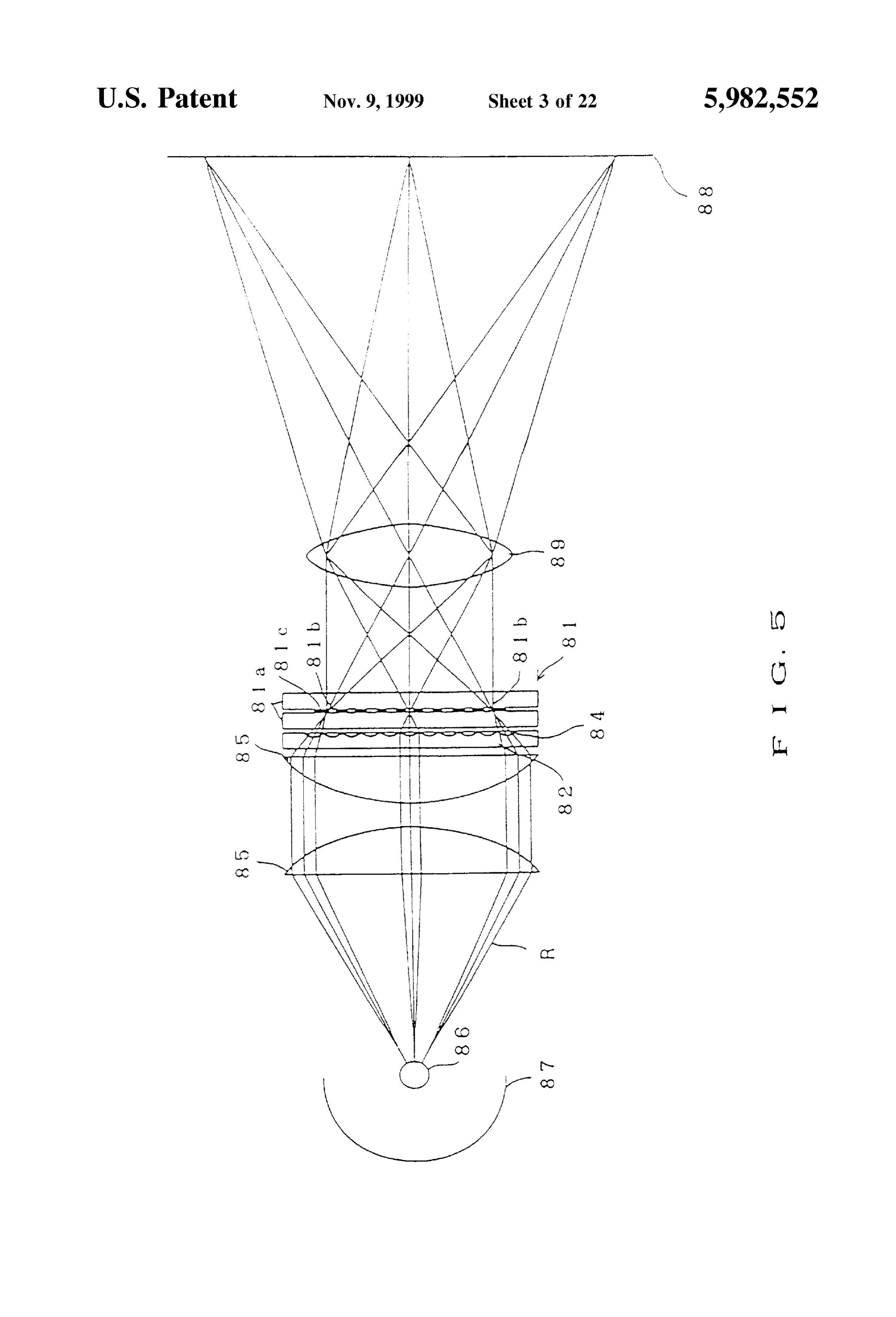
This application is a division of U.S. application Ser. No. having Such a planar microlens array is shown in FIG. 5. 08/700,397 filed on Dec. 13, 1996 now U.S. Pat. No. 5 In FIG. 5, the light emitted by a light source 86 is 5,867,321. converged by a reflecting mirror 87 and a condenser lens 85 so as to direct toward a projection lens 89. The light flux
TECHNICAL FIELD passing through the condenser lens 85 is converged by a The present invention relates generally to a planar micro planar microlens array 82 onto a pixel aperture area (pixel lens array and a method of making the Same, and more two aperture) 81b of a liquid crystal element formed between particularly to a planar microlens array that is useful as a substrates 81a of a liquid crystal panel 81, and projected converging lens to converge light for illuminating a trans onto a screen 88 by the projection lens 89. missive image display panel, Such as a liquid crystal display By using a planar microlens array as described above, the panel having a plurality of pixels, onto pixel apertures to light flux that would otherwise been shielded by the pixel make the liquid crystal display panel brighter, and a method 15 shielding area 81c of the liquid crystal display panel 81 can of making the Same. be converged onto the pixel aperture area 81b. As a result,
BACKGROUND ART
the light flux reaching the screen 88 increases 2 to 2.5 times as much as that without the planar microlens array 82.
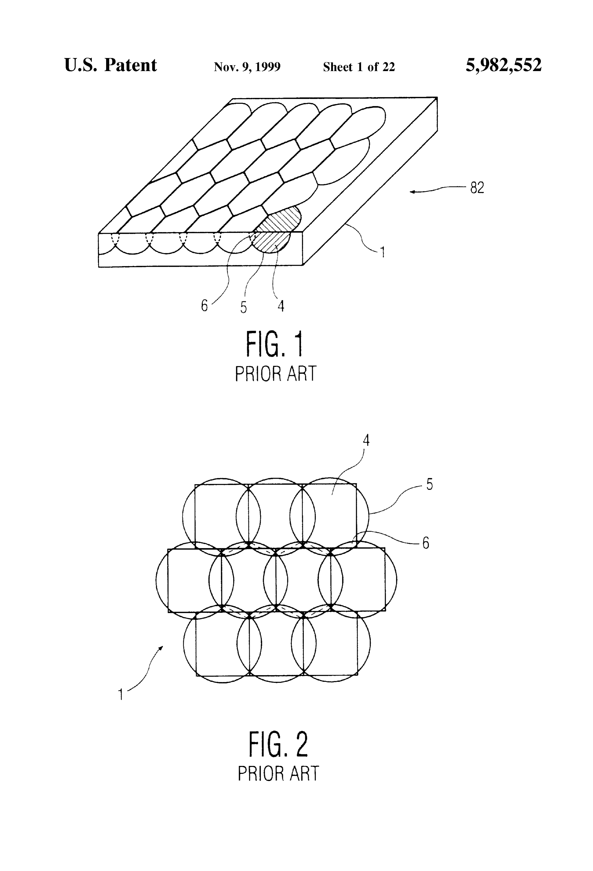
This type of planar microlens array was disclosed by The technologies disclosed in Japanese Patent Publication Hamanaka, et al. in Japanese Patent Publication No. No. 3-136004 and Japanese Patent Publication No. 5-45642 3-136004 (Refer to FIG. 1). The planar microlens array are intended to improve overall converging efficiency in disclosed in the Publication is manufactured using the ion converging light onto the pixel apertures of the liquid crystal diffusion process. In the ion diffusion process, a glass element. To further improve converging efficiency, it is Substrate is used as a transparent Substrate 1 on the Surface generally necessary to further increase the lens filling rate of of which a diffusion-inhibiting mask film comprising Ti, Al, 25 the planar microlens array. With the Six-lobe lens array as Ni or Cr, etc. is formed using the Sputtering and other disclosed in Japanese Patent Publication No. 3-136004, the thin-film forming processes, and then a desired array of lens filling rate is almost 100%, with virtually no room left circular mask apertures is formed on the diffusion-inhibiting for further improvement. In terms of the improvement of mask film. After that, the transparent Substrate is immersed overall converging efficiency, however, there still remains a for a predetermined period of time in a molten-Salt bath problem. That is, regions where the diffusion fronts of the containing ions contributing to increasing the refractive adjoining lenses are fused together contribute little to the index of the Substrate. AS ions in the molten-Salt bath are conversion of light onto the pixel apertures that is illumi diffused through the mask apertures in the transparent nated because of their high astigmatism due to lowered Substrate, a planar microlens array 82 having a plurality of rotational Symmetry of the concentration distribution of microlenses of a refractive-indeX distribution type with 35 diffused ions. In other words, an increase in the area where decreasing refractive indeX from the vicinity of the center of diffusion fronts are fused together could lead to a decrease, each mask aperture toward the circumference thereof is far from an improvement, in overall converging efficiency, formed. In a liquid crystal display panel having a delta even with 100% of the lens filling rate.
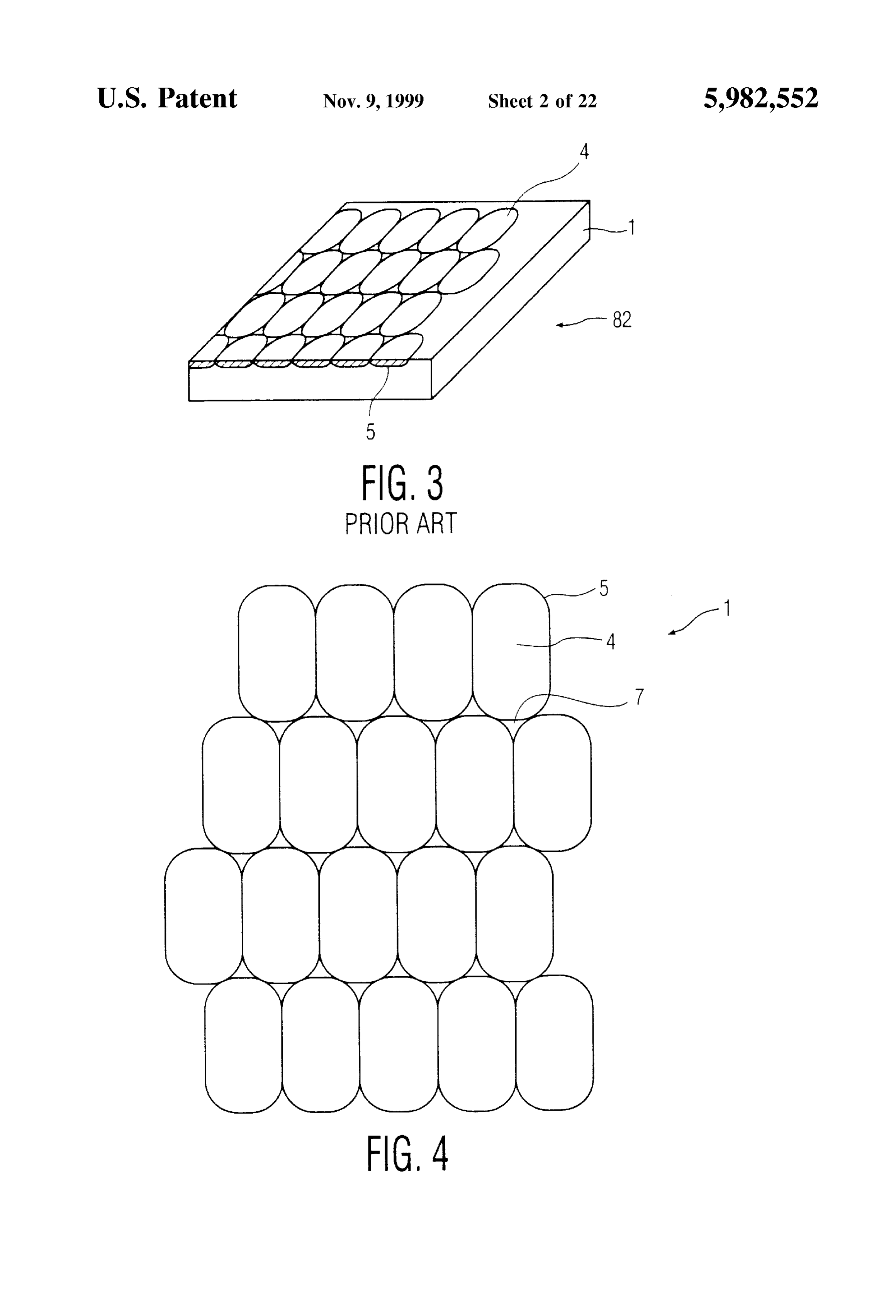
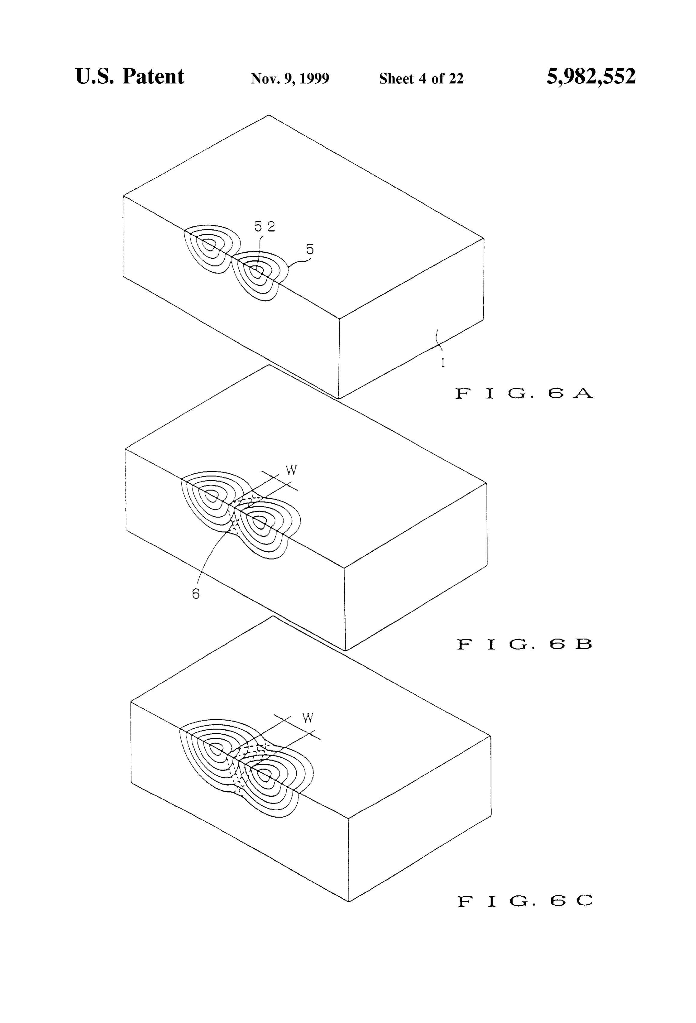
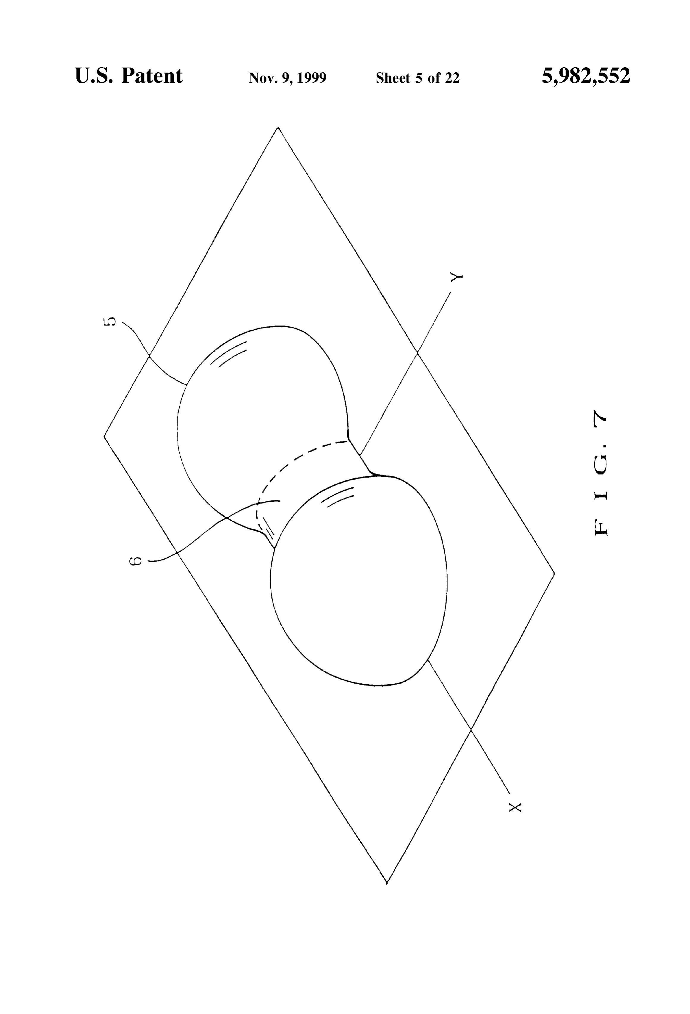
(six-lobe) pixel array, this planar microlens array has micro Now, a model for forming two microlenses on a flat lenses of a hexagonal circumferential shape that are 40 Substrate with an ion diffusion proceSS using circular mask arranged two-dimensionally, regularly and densely on the apertures will be taken up as an example for simplicity. surface of the transparent substrate, as shown in FIG. 1. In FIGS. 6A through 6C are partially cross-sectional perspec this case, the lens array is a six-lobe array. tive ViewS illustrating the State where two microlenses are The circumferential shape of each microlens can be made formed on a transparent Substrate 1. Ions are diffused into a desired hexagonal shape by providing a region 6 45 through a circular mask aperture as a diffusion center 52, and where the diffusion fronts 5 that are leading edges of the diffusion fronts 5 that are leading edges of diffusion areas microlension diffused areas of the adjoining microlenses 4 Spread in concentrical Semispheres. With the progreSS of ion are fused together, as shown in FIG. 2. In this case, lens diffusion, the two diffusion fronts eventually come into filling rate, the ratio of the area occupied by microlenses to contact with each other (FIG. 6A). As ion diffusion further the total area of the transparent Substrate on which lenses are 50 proceeds, the diffusion fronts are fused together, and the ion formed, is almost 100%. concentration gradient in the direction of a line connecting Oikawa et al., on the other hand, disclosed a planar the adjoining diffusion centerS decreases in the fused area. microlens array for use in liquid crystal display panels in Thus, the diffusion Speed in that direction decreases, and as Japanese Patent Publication No. 5-45642 (Refer to FIG. 3). a result, the diffusion fronts in the fused area form a A planar microlens array 82 is formed with the ion diffusion 55 continuum of curved Surface, expanding in the direction process using a diffusion-inhibiting mask film having orthogonally interSecting the aforementioned direction (in formed oblong mask apertures. This planar microlens array the direction of the boundary line with the adjoining lens) 82 has microlenses 4 of an oblong circumferential shape, as (FIGS. 6B and 6C). FIG. 7 is a perspective view illustrating shown in FIG. 4, by terminating ion diffusion in the state a solid body formed by the diffusion fronts viewed from the where diffusion fronts of the adjoining microlenses come in 60 direction opposite to the Surface on which lenses are formed. contact with each other. With this, the lens filling rate is short The area in which these diffusion fronts have been fused of 100% because of the existence of a lens unformed region together is called an overlapped diffusion area 6. The length where no lenses are formed, but a planar microlens array 82 of the overlapped diffusion area 6 in the direction of a line having a relatively high lens filling rate is formed Since the connecting the lens centers is called the width W of the lens array is of a six-lobe type. 65 overlapped diffusion area 6.
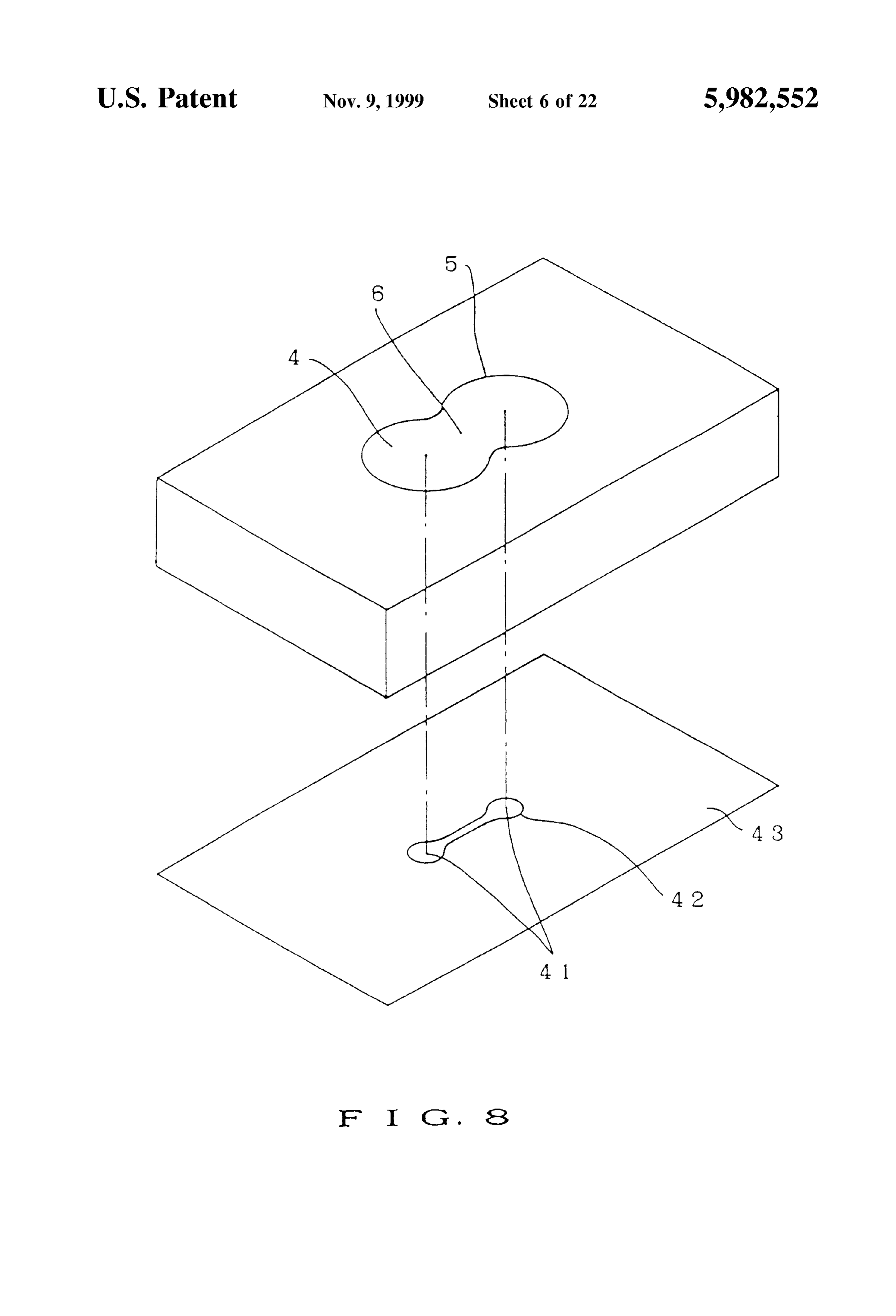
These planar microlens arrays are Suitable for condenser As the overlapped diffusion area 6 receives ions fed by lenses to illuminate display images by converging light to both the diffusion centers 52 as the ion Sources, the concen
Page 25
tration distribution of diffused ions forms a gentle saddle The method of manufacturing planar microlens arrayS shape in the direction of a line connecting the lens centers (in according to the present invention is characterized in that the the X direction shown in FIG. 7). The overlapped diffusion manufacturing method includes a Step for preparing a planar area 6 has a lower refracting power than an equivalent transparent Substrate, a step for assuming that the desired independent microlens, causing a remarkable astigmatism, circumferential shape of microlenses being formed is a because of the Smaller gradient of its ion concentration polygon, and forming on the Surface of the Substrate a distribution in the X direction. Consequently, the light diffusion-inhibiting mask film having within the polygon a incident on this overlapped diffusion area 6 hardly converge multitude of regularly arranged mask apertures of a shape on the neighborhood of the focal point of each lens on which defined by straight lines parallel with the sides of the the light is originally to converge, but on a narrow Strip-like polygon and having predetermined intervals from the Sides area connecting the centers of the adjoining lenses. The of the polygon, and a Step for forming microlenses over the model of this state is shown in FIG.8. In the figure, numeral practically entire Surface of the Substrate by diffusing in the 41 denotes a focal point of the microlens 4, 42 a converging Substrate through the mask apertures a material contributing area of the microlens, and 43 a converging plane, respec to increasing the refractive index of the Substrate. tively. The light incident on the overlapped diffusion area 6 15 The method of manufacturing planar microlens arrayS also converges on a Strip connecting the focal points 41. according to the present invention is characterized in that the DISCLOSURE OF THE INVENTION manufacturing method includes a Step for preparing a planar It is an object of the present invention to provide a planar transparent Substrate, a step for assuming that the desired microlens array having a high converging efficiency regard circumferential shape of microlenses being formed is a first less of how the planar microlens array is arranged. polygon and a Second polygon defined by Straight lines It is another object of the present invention to provide a parallel with the Sides of the first polygon and having planar microlens array having an excellent overall converg predetermined intervals from the Sides thereof, and forming ing efficiency, in which the converging efficiency of lens is on the Surface of the Substrate a diffusion-inhibiting mask not lowered even when the ratio of the area occupied by 25 film having having a multitude of regularly arranged mask apertures a shape defined by curves or broken lines passing the microlenses to the area of the Substrate on which micro lenses are formed, that is, the lens filling rate is increased. inside of the Second polygon, rather than a line connecting It is still another object of the present invention to provide the adjoining apexes of the Second polygon, and a step for a method of manufacturing planar microlens arrays having forming lenses over the practically entire Surface of the Substrate by diffusing in the Substrate through the mask an excellent overall converging efficiency. apertures a material contributing to increasing the refractive The present invention is characterized by a planar micro index of the Substrate.
lens array having arranged two-dimensionally and regularly on the Surface of a planar transparent Substrate a multitude BRIEF DESCRIPTION OF THE DRAWINGS of refractive-index distribution type microlenses formed by diffusing in the Substrate a material contributing to increas 35 FIG. 1 is a perspective view of a prior-art planar microlens ing the refractive index of the substrate, in which the array.
microlenses are densely arranged on the Substrate Surface, FIG. 2 is a plan view of the planar microlens array shown the diffusion front of each microlens is fused with the in FIG. 1.
diffusion front of an adjoining microlens to form a fused FIG. 3 is a perspective view of another prior-art planar area, and the length in the direction of a line connecting the 40 microlens array.
centers of the microlenses of the fused area of certain two adjoining microlenses is less than 20% of the array pitch. FIG. 4 is a plan view of the planar microlens array shown in FIG. 3.
The present invention is characterized by a planar micro FIG. 5 is a cross-sectional view of optical paths in an lens array having arranged two-dimensionally and regularly image display device.
on the Surface of a planar transparent Substrate a multitude 45 of refractive-index distribution type microlenses formed by FIGS. 6A through 6C are partially cross-sectional per diffusing in the Substrate a material contributing to increas Spective views illustrating a model of assistance in explain ing the refractive index of the substrate, in which the ing the State where diffusion fronts are fused together. microlenses are arranged virtually densely on the Surface of FIG. 7 is a perspective view illustrating a solid body the Substrate, and the diffusion front of each microlens 50 formed when the diffusion fronts have been fused together. comes in contact with the diffusion front of an adjoining FIG. 8 is a perspective view of a model of assistance in microlens in a Straight line without fusing with each other. explaining the State of an ideal fusion from a rectangular The method of manufacturing planar microlens arrayS mask aperture.
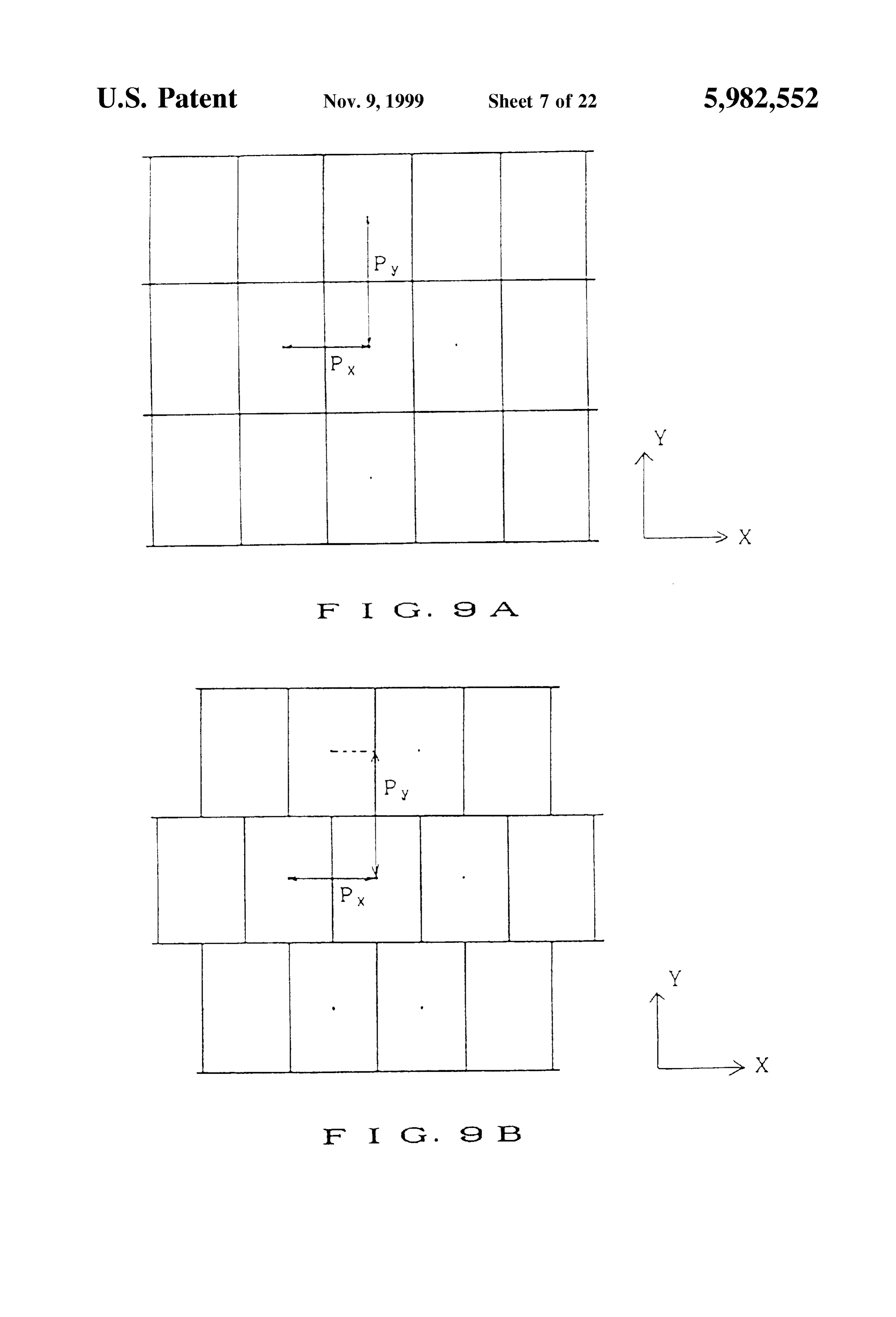
according to the present invention is characterized in that the FIG. 9A is a diagram illustrating a four lobe array of manufacturing method includes a Step for preparing a planar 55 lenses.
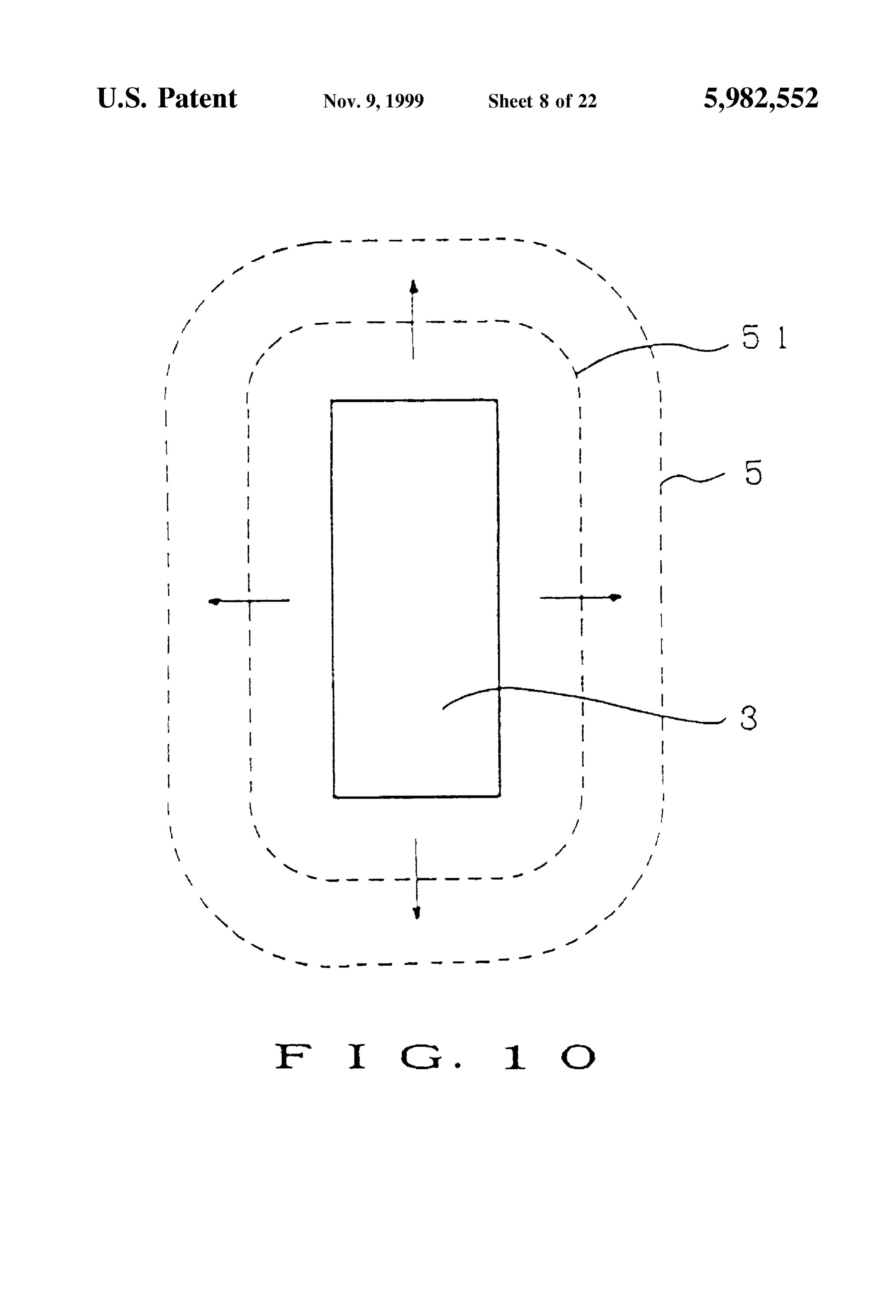
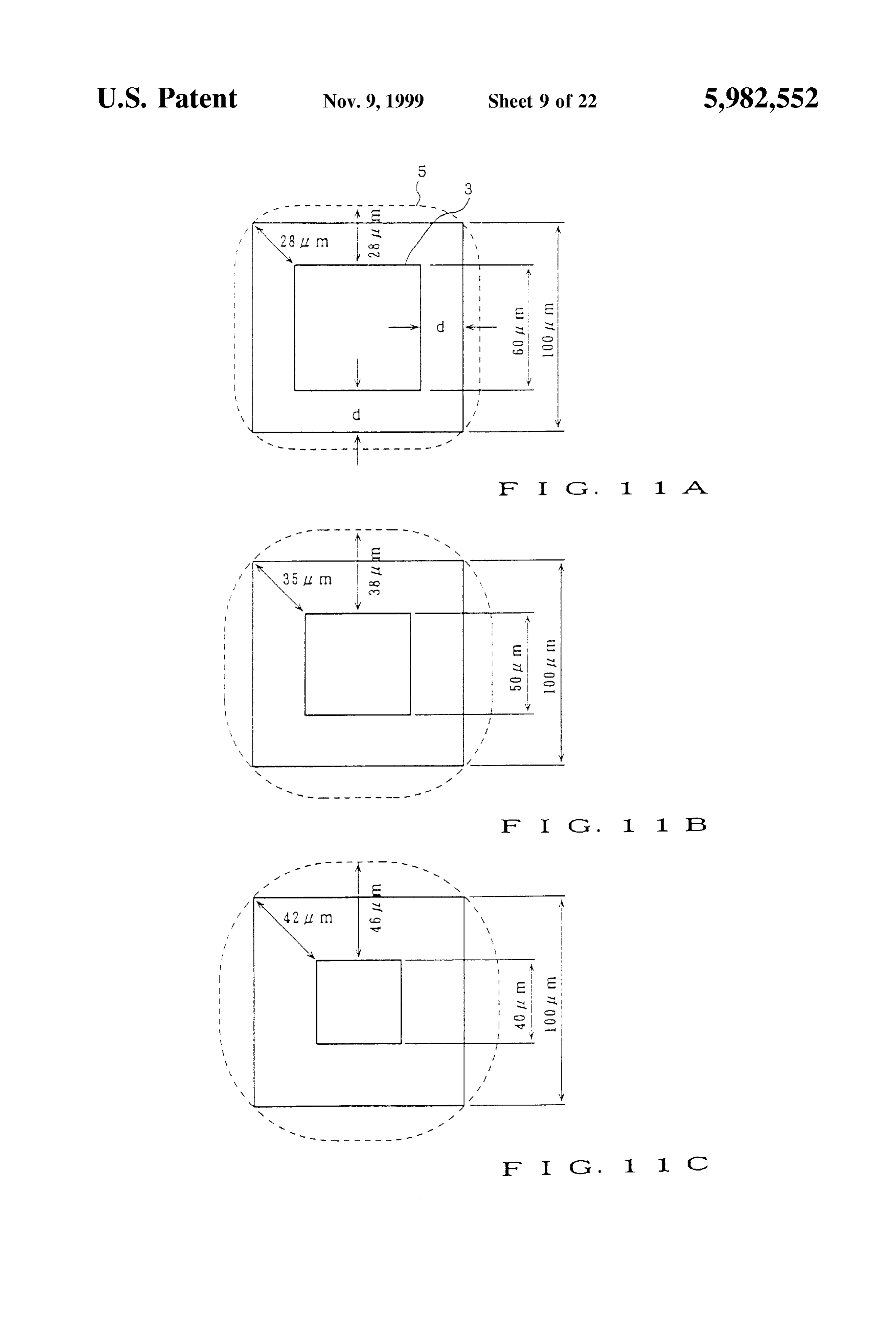
transparent Substrate, a step for forming a diffusion FIG.9B is a diagram illustrating a six-lobe array of lenses. inhibiting mask film having a multitude of two FIG. 10 is a model diagram of assistance in explaining the dimensionally regularly arranged mask apertures on the State of an ideal fusion from a rectangular mask aperture. Surface of the Substrate, and a step for forming microlenses of a polygonal circumferential shape over the practically 60 FIGS. 11A through 11C are diagrams illustrating the state entire surface of the substrate by diffusing in the substrate where a diffusion front having rounded cornerS is formed from the mask apertures a material contributing to increas from a rectangular mask aperture.
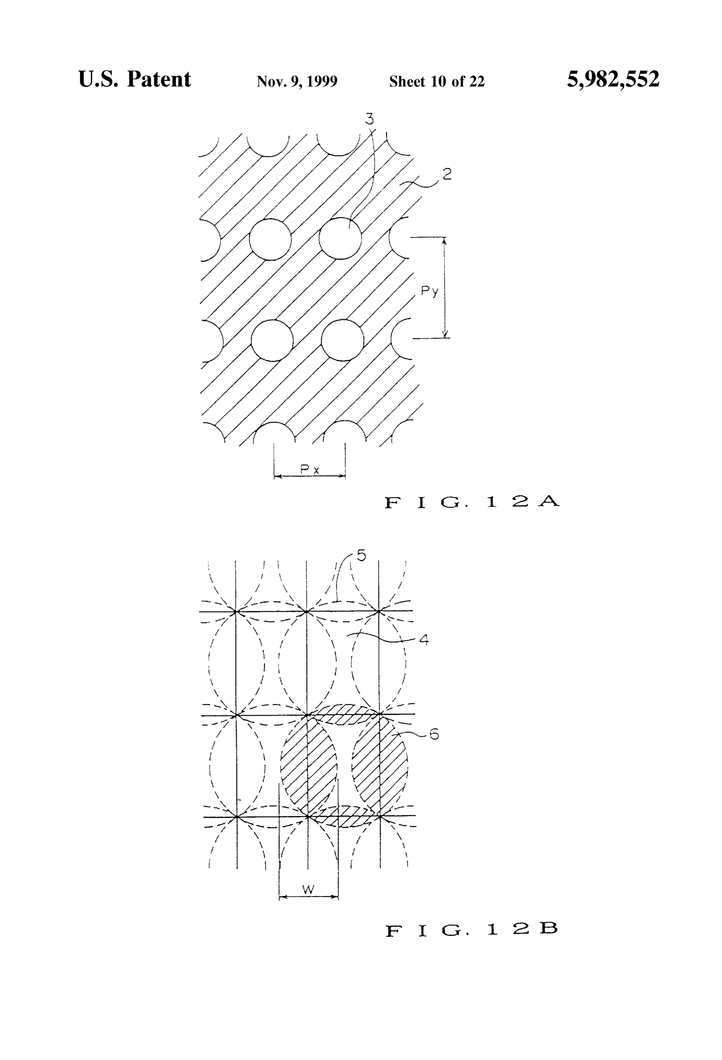
ing the refractive indeX of the Substrate; in the Step of FIG. 12A is a diagram illustrating a diffusion-inhibiting forming the diffusion-inhibiting film, the shape of the mask mask film having circular mask apertures apertures being Set So that the diffusion fronts corresponding 65 FIG. 12B is a diagram illustrating a four lobe planar to the sides of the microlenses being formed are arranged in microlens array prepared using the diffusion-inhibiting mask a Straight line. film shown in FIG. 12A.
Page 26
S 6
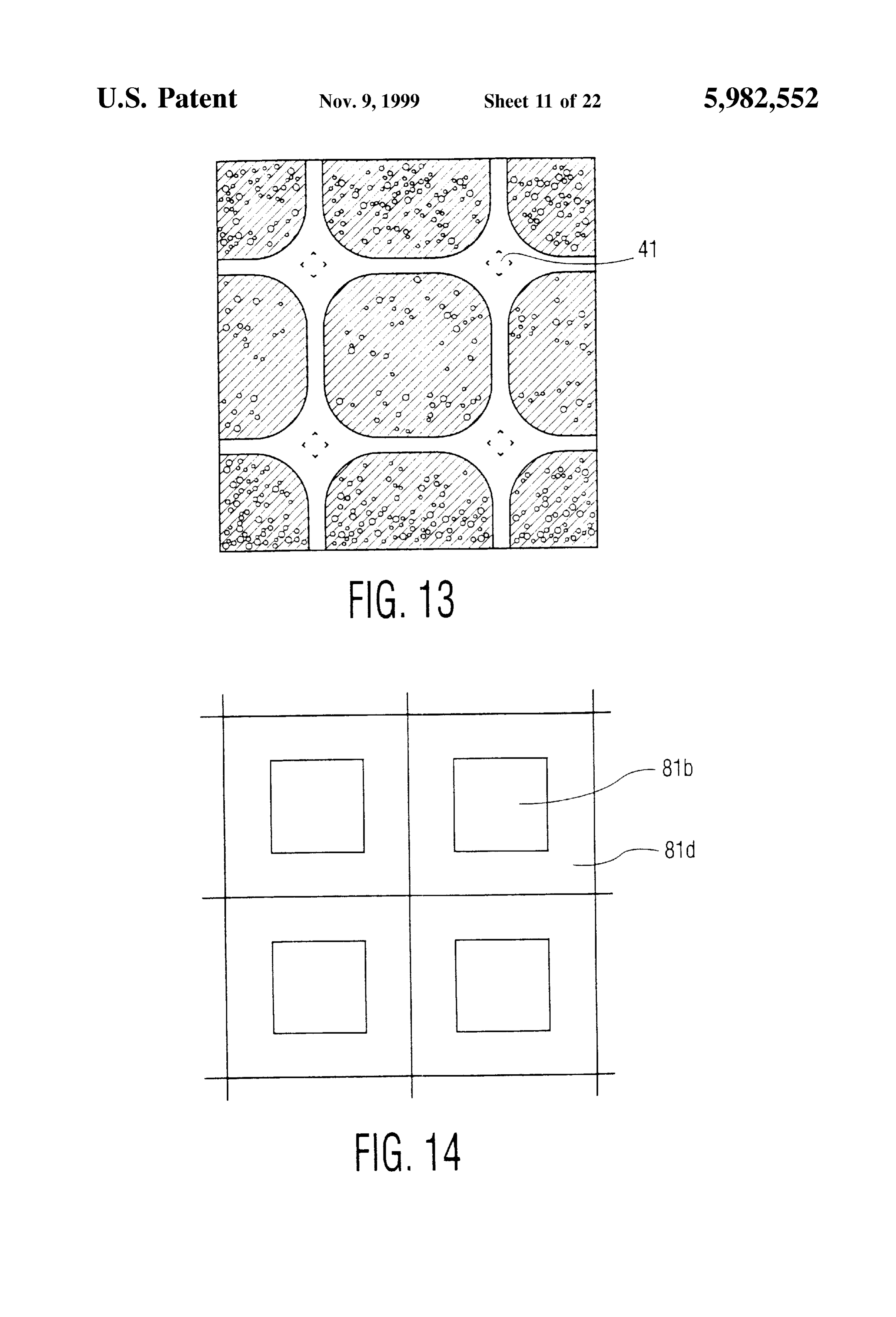
FIG. 13 is a diagram illustrating converged light spots X-Y coordinate system, and FIG. 9B shows a six-lobe array obtained through a planar microlens array comprising Square of lenses that are rectangular in the circumferential shape on lenses prepared using a diffusion-inhibiting mask film hav the orthogonal X-Y coordinate System. In the figure, P. ing circular apertures. denotes an array pitch in the X-axis direction, P, an array FIG. 14 is a diagram illustrating the relationship between pitch in the Y-axis direction, respectively. pixels (microlenses) and pixel apertures. Now, the aspect ratio of a lens having a rectangular FIG. 15A is a diagram illustrating a diffusion-inhibiting circumferential shape will be described. When it is assumed mask film having oblong mask apertures. that the length of short Sides of the lens is a and the length of the longsides is b, then C. (=b/a) is called the aspect ratio.
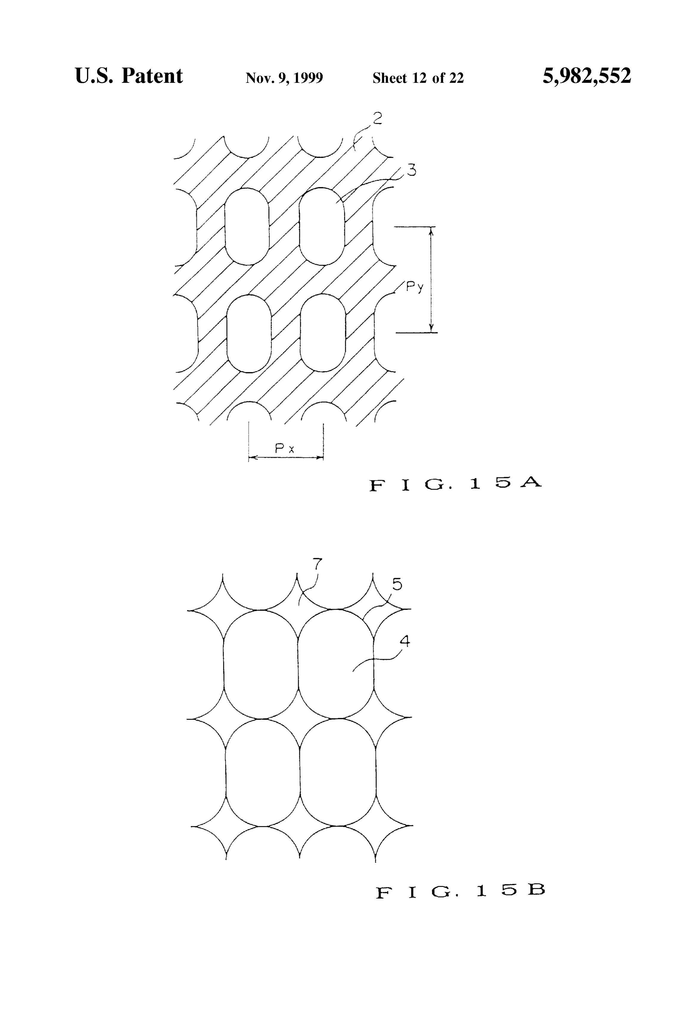
FIG. 15B is a diagram illustrating a four lobe planar When this aspect ratio C. is large, a planar microlens array microlens array prepared using the diffusion-inhibiting mask having a relatively large effective area and a good converg film shown in FIG. 15A. ing efficiency can be manufactured by using masks having FIG. 16A is a diagram illustrating a diffusion-inhibiting oblong apertures, as disclosed in Japanese Patent Publica mask film for preparing a planar microlens array embodying tion No. 5-45642.
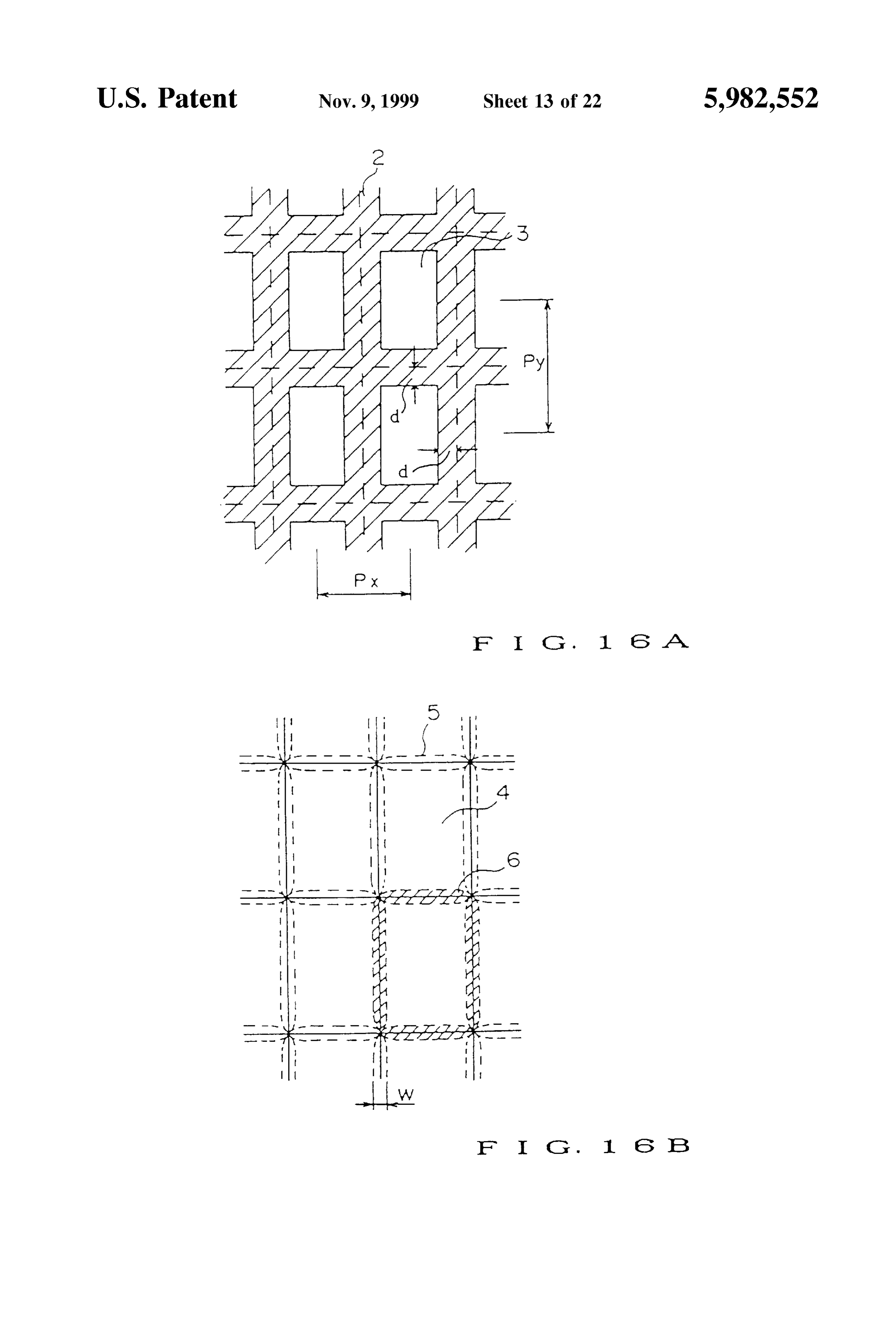
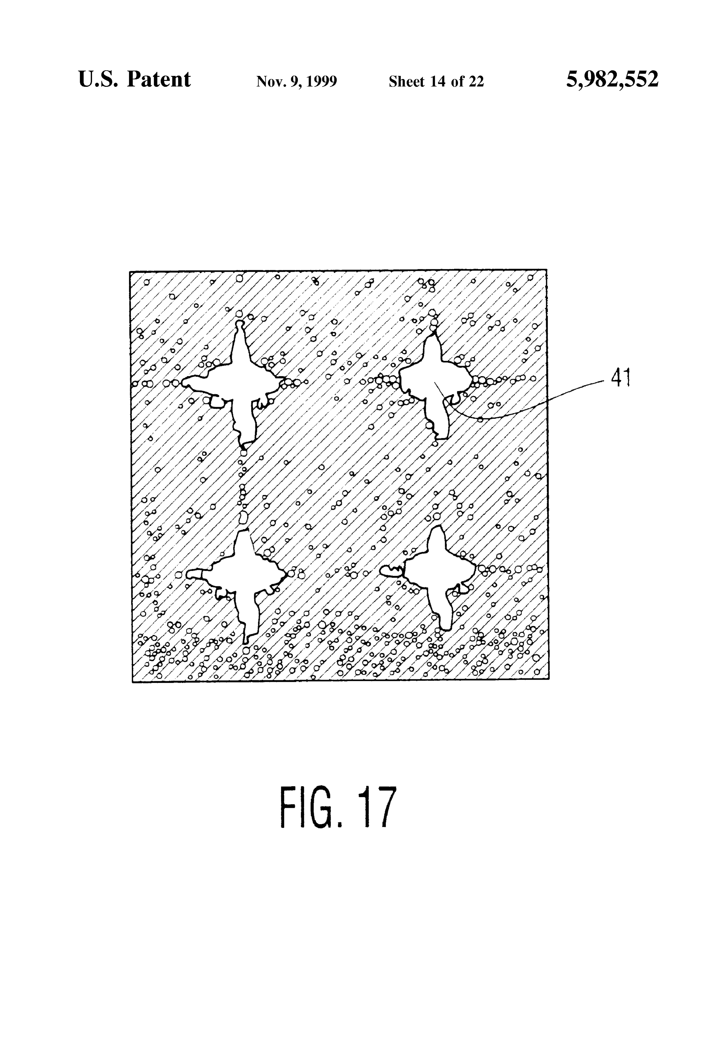
the present invention. 15 Typical planar microlens arrays Suitable for liquid-crystal FIG. 16B is a diagram illustrating a planar microlens array display panels largely have lenses of aspect ratioS of leSS prepared using the diffusion-inhibiting mask film shown in than 2. The relationship between the aspect ratio and the FIG. 16A. filling rate of lenses manufactured using masks having FIG. 17 is a diagram illustrating converged light spots oblong apertures, as disclosed Japanese Patent Publication obtained through the planar microlens array shown in FIG. shown in Tablein 1.the four-lobe array of rectangular lenses is
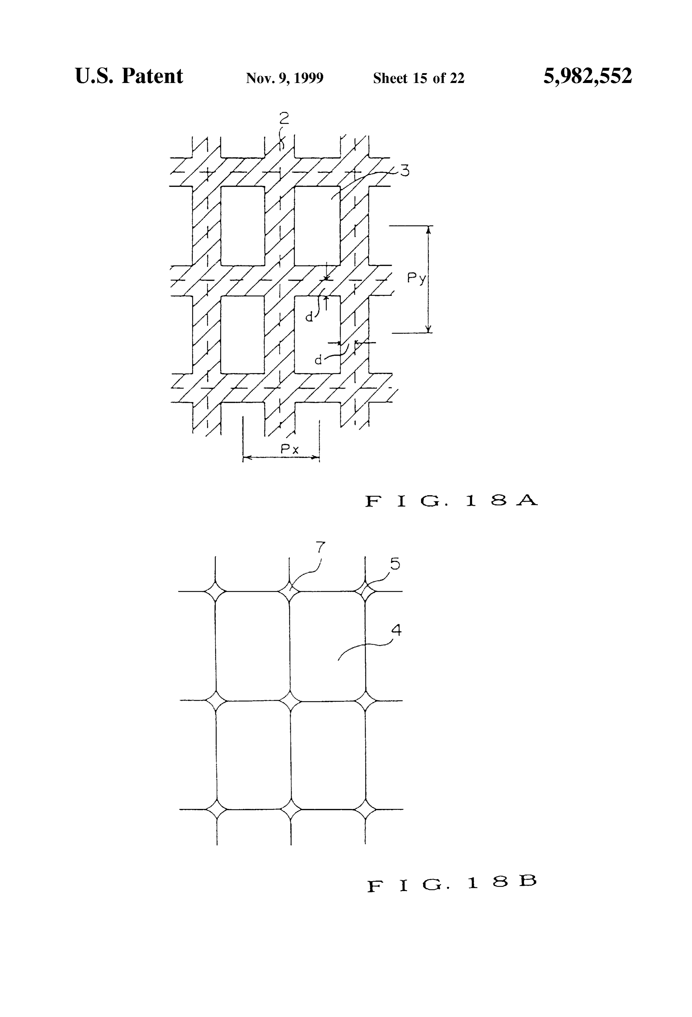
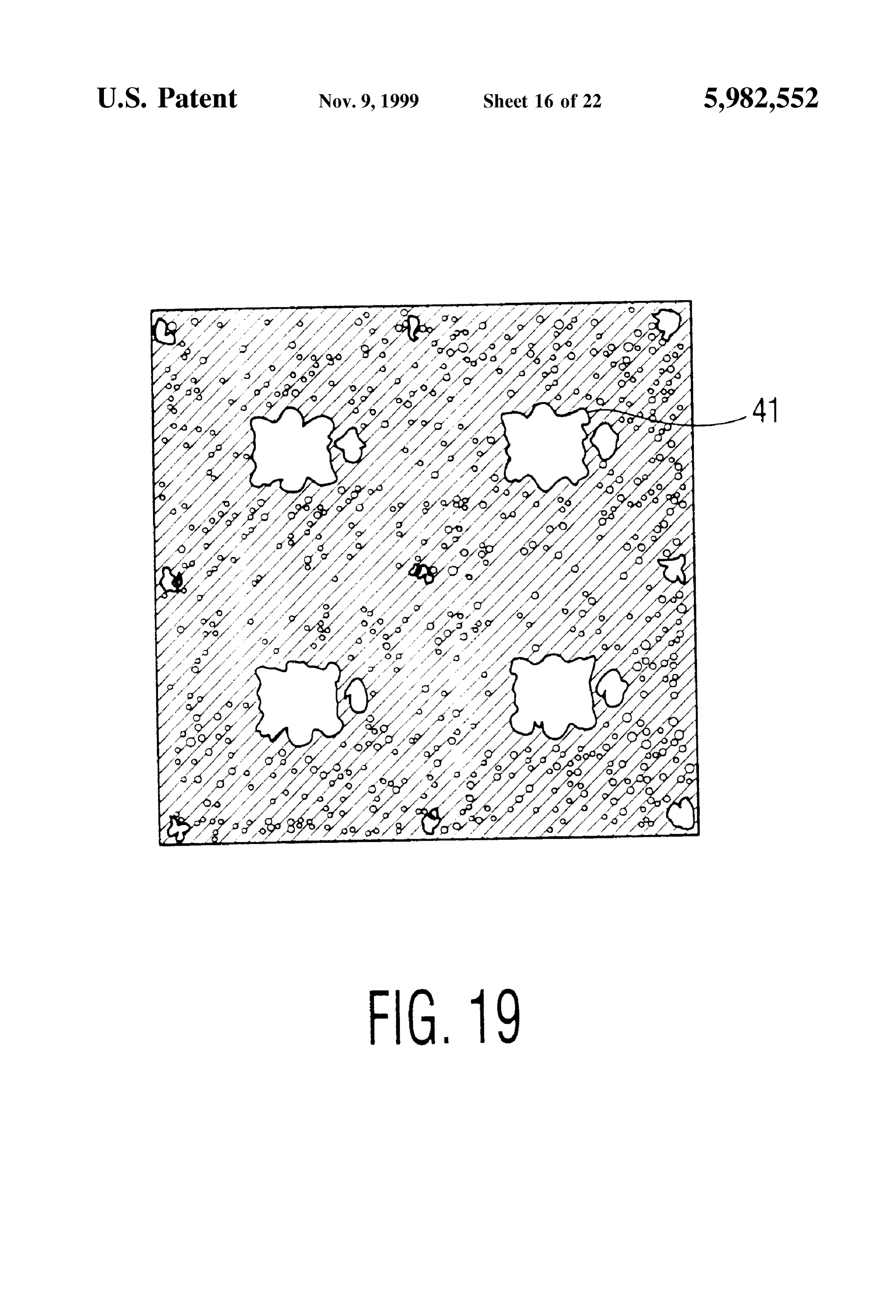
FIG. 18A is a diagram illustrating a diffusion-inhibiting TABLE 1. mask film for preparing a planar microlens array that is still another embodiment of the present invention. The relationship between the aspect ratio and filling rate of FIG. 18B is a diagram illustrating a planar microlens array 25 lens (in the four-lobe array of rectangular lenses prepared using the diffusion-inhibiting mask film shown in Aspect Lens filling Aspect Lens filling FIG. 18A. ratio C. rate ratio C. rate FIG. 19 is a diagram illustrating converged light spots 1.O 0.785 1.6 O.866 obtained through the planar microlens array shown in FIG. 1.1 O.805 1.7 O.874 18B. 1.2 O.821 1.8 O.881
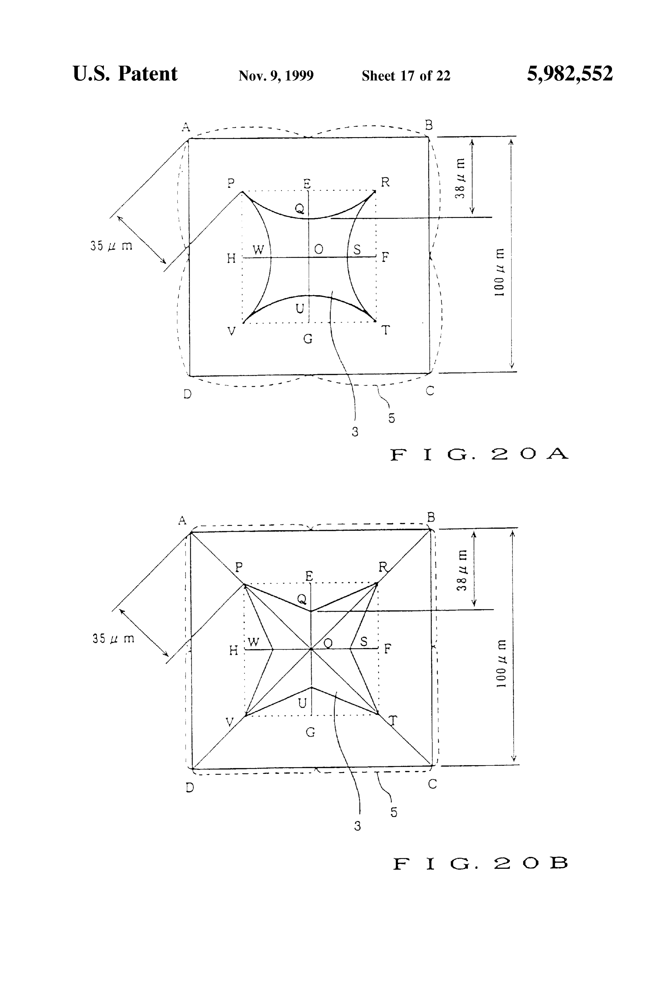
FIGS. 20A and 20B are diagrams illustrating still another 1.4 O.847 2.0 O.893 embodiment of the planar microlens array according to the 1.5 0.857 present invention.
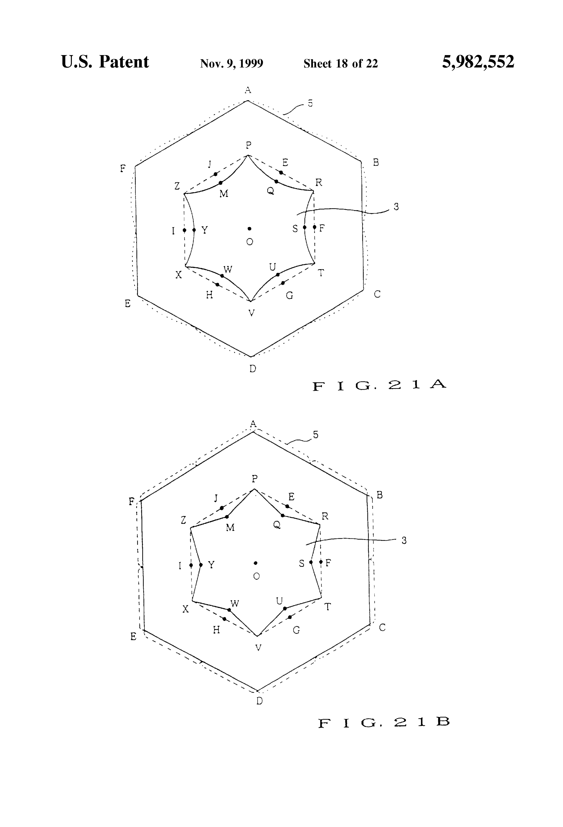
FIGS. 21A and 21B are diagrams illustrating still another 35 The table indicates that as the lens aspect ratio increases embodiment of the planar microlens array according to the from 1.0 to 2.0, the lens filling rate increases. present invention. Next, the shape of mask apertures will be discussed. FIGS. 22A and 22B are diagrams illustrating still another The microlens array disclosed in Japanese Patent Publi embodiment of the planar microlens array according to the cation No. 3-136004 is of a six-lobe array where the present invention. 40
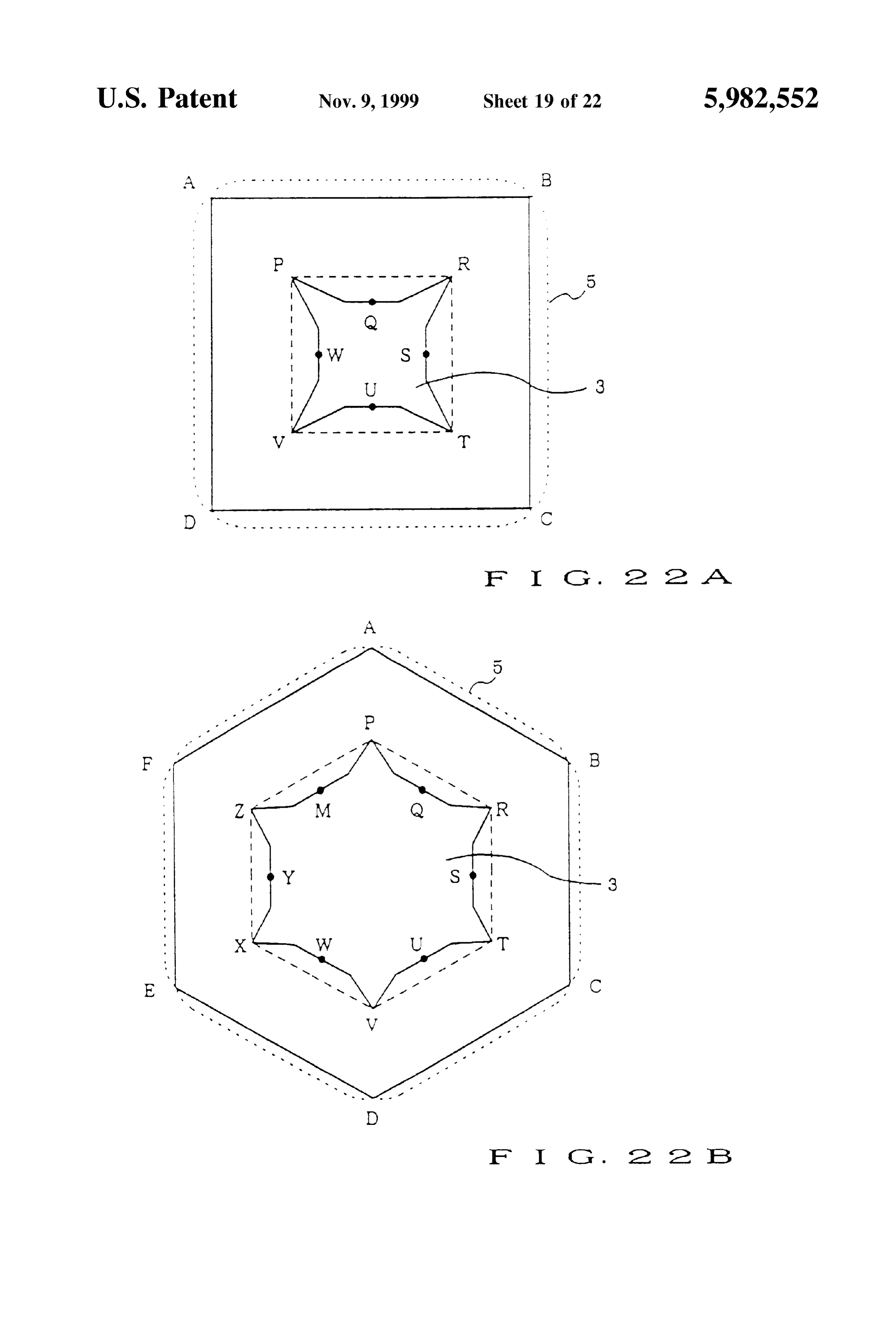
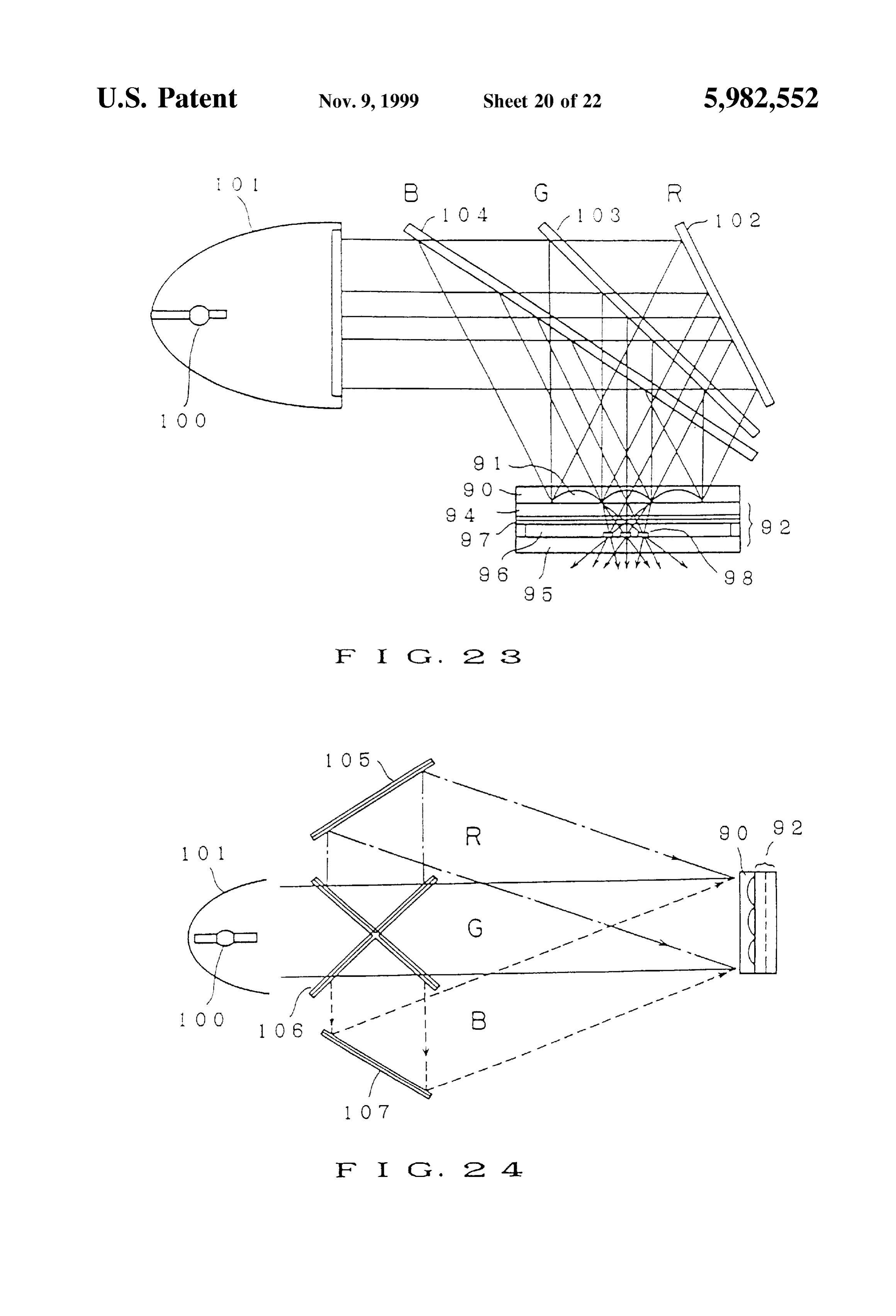
FIG. 23 is a block diagram illustrating an example where shape of mask aperturesofis microlenses circumferential shape circular.
is hexagonal. The a planar microlens array according to the present invention In the meantime, the shape of mask apertures when is applied to an image display device. manufacturing with the diffusion process lenticular lenses of FIG. 24 is a diagram illustrating another layout of a 45 a virtually Semi-circular cross-sectional shape is linear (refer dichroic mirror.
to FIG.3 in Japanese Patent Publication No. 61-201639, for
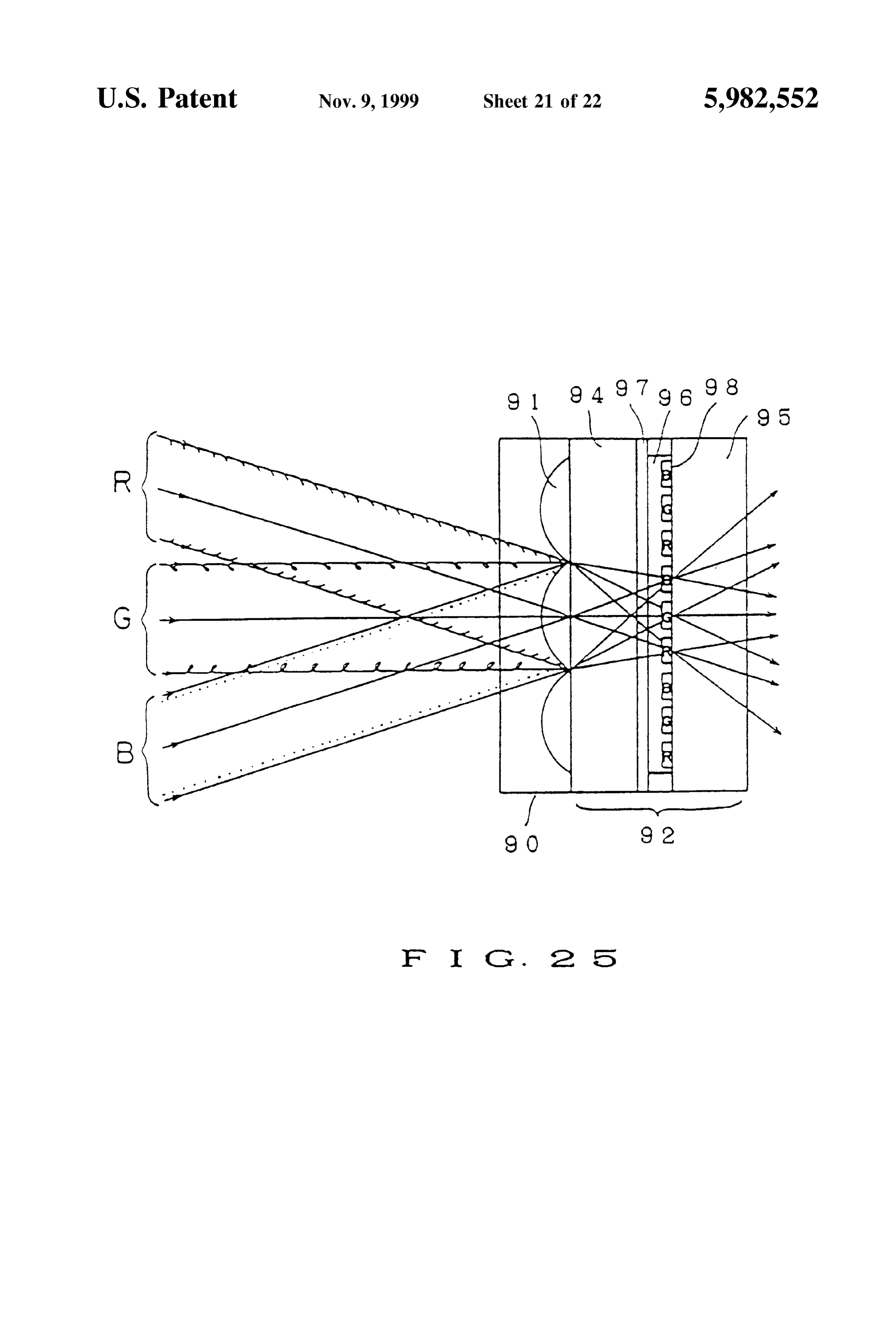
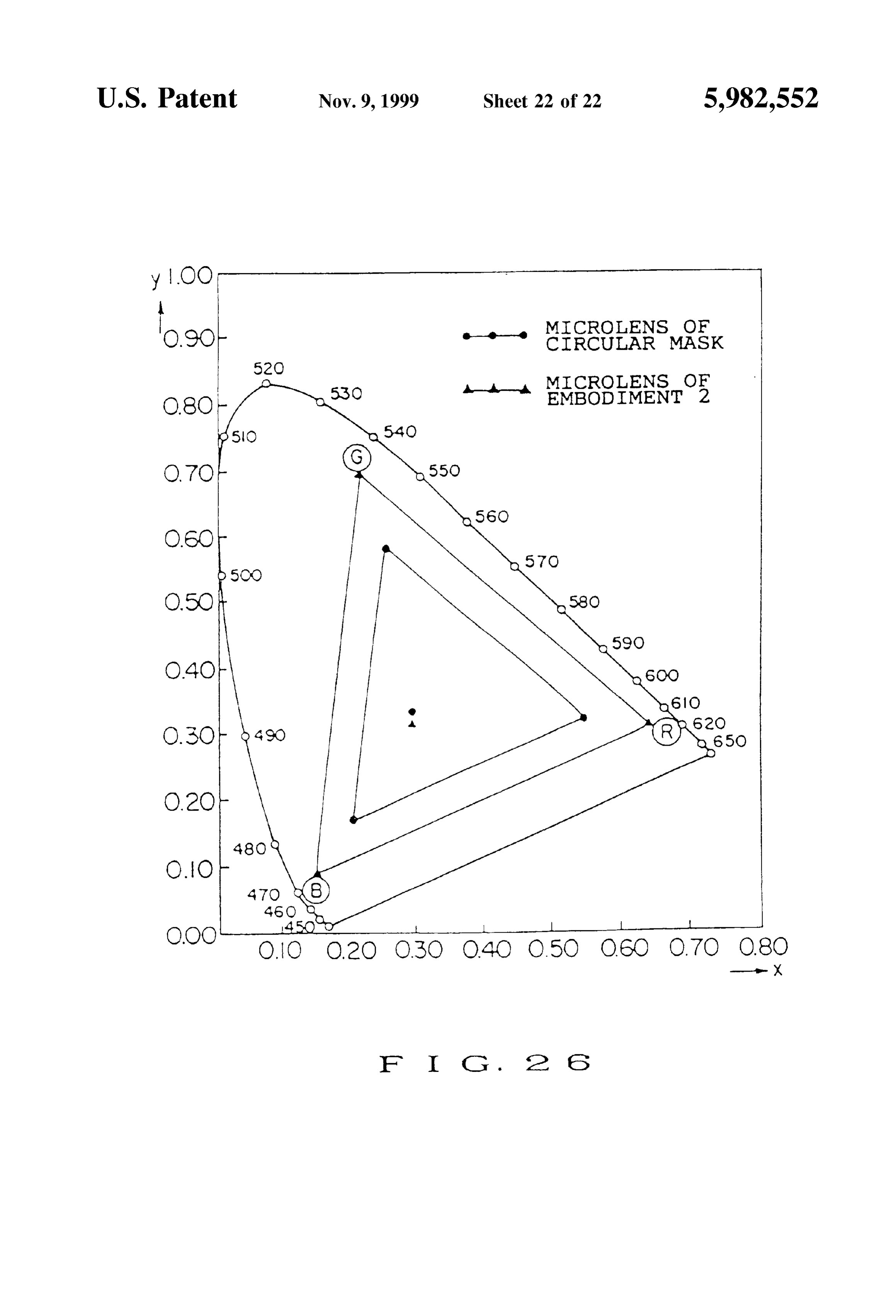
FIG. 25 is a diagram illustrating the state where con example.) A detailed study of the state of diffusion at this verged light spots of the fluxes of R, G and B colors are time reveals that a diffusion front diffused through a given incident on the respective pixel apertures corresponding to mask aperture proceeds linearly in parallel with the linear the colors. 50 mask aperture. AS the diffusion process further proceeds, FIG. 26 is a chromaticity diagram of assistance in explain that diffusion front comes in contact with another diffusion ing the effects of an image display device using a microlens front through an adjacent mask aperture. Thus, lenticular array according to the present invention. lenses can be formed without gaps over the entire Surface of the Substrate.
BEST MODE FOR CARRYING OUT THE
INVENTION 55 The inventors of this application further advanced this idea and invented the present invention by Switching from
In a planar microlens array according to this invention, a the prior-art mask apertures of a circular or oblong shape to multitude of lenses are densely, two-dimensionally and mask apertures of a rectangular shape in order to form lenses regularly arranged. Typical two-dimensional regular lens two-dimensionally without gaps over the entire Surface of arrays include the four-lobe array and the six-lobe array. The 60 the Substrate. FIG. 10 shows an ideal diffusion model from four-lobe array is Such that when one lens is noted from a mask aperture of a rectangular shape. Rounded corners of among lenses in the array, there are four lenses adjacent to the diffusion front 5 in this figure are attributable to the fact that lens. The Six-lobe array is Such that when one lens is that ions are spot-diffused Starting from the four corners of noted from among lenses in the array, there are Six lenses the mask aperture 3. In the figure, numeral 51 denotes an adjacent to that lens. 65 iso-refractive-indeX curve.
FIG. 9A shows a four-lobe array of lenses that are If the dimensions of mask apertures of a rectangular rectangular in the circumferential shape on the orthogonal (Square or rectangular) shape are relatively Small, contribu
Page 27
tion of the rounded corner of a diffusion corner increases, in which a thin film of a diffusion material is formed at with the result that the entire diffusion-front shape becomes positions corresponding to mask apertures, or the monomer dull. diffusion copolymerization process (Japanese Patent Publi This will be described taking as an example a microlens cation No. 2-50102, for example) in which after a plastic of a 100 limx 100 um in circumferential shape. FIG. 11A 5 Substrate is obtained by Semi-polymerizing a first monomer shows a diffusion front 5 (mask aperture 3: a 60 umx60 um on a transparent Substrate, and then a Second monomer is Square, distance d between the neighborhood of lens and diffused over the plastic Substrate to complete polymeriza mask aperture: 20 um, and diffusion length: 28 um). The tion may also be employed. In Short, any methods of front 5 of the diffusion region extending from the mask diffusing over a transparent Substrate a material contributing aperture 3 becomes a rectangular-shaped region, with to increasing the refractive index of the Substrate to form a rounded corners, that is obtained by adding an area equal to planar microlens array having a refractive-indeX gradient the diffusion length to the periphery of the mask aperture. based on the concentration gradient of the material may be With the dimensions of microlenses being the same, used.
Furthermore, the mask aperture according to the present however, if the distance d is increased to obtain a relatively 15 invention
Small rectangular mask aperture, the contribution of the Spot may be of a polygonal shape having Straight diffusion effect at corners increases, and as a result, the chamfered portions about a few um long or minute circular shape of the diffusion front becomes dull, approaching a effects arc portions on the apexes thereof, with no differences in its circle. FIGS. 11B and 11C show the approximate shapes of between them.
diffusion fronts when mask apertures are a 50 timx50 um (Preliminary tests)
Square and a 40 limx40 um Square, respectively, and the Prior to the description of embodiments of the present diffusion length is set So that the diffusion regions becomes invention, the problem of the converging efficiency of lens Sufficiently dense with Virtually no gaps. AS is apparent from will be discussed based on the results of preliminary tests the figures, when the shape of a mask aperture is Small, the conducted to compare the present invention with the prior overlapped diffusion regions become larger, making it dif art. Now, a planar microlens array as shown in Japanese ficult to obtain a good converging effect. This holds true not 25 Patent Publication No. 3-136004, to which a four-lobe array only for rectangular shapes but also for other polygonal of lenses having a rectangular circumferential shape is shapes. applied, will be taken as an example. FIG. 12A is a plan view In this way, with the relatively smaller shape of mask of a diffusion-inhibiting mask film, FIG. 12B is a plan view apertures, compared with the circumferential shape of of a planar microlens array prepared using this diffusion inhibiting mask film.
microlenses, if the overlapped diffusion regions become As shown in FIG. 12A, ions were diffused through larger due to the dulled corners of the diffusion fronts, that circular mask apertures 3 arranged at pitches P and P in X is, the contribution of the Spot diffusion effect, it is necessary and Y directions, and overlapped diffusion regions 6 were to modify the shape of mask apertures. provided between adjoining microlenses 4, as shown in FIG. In Such a case, by modifying the shape of mask apertures 35 12B, so that the lens filling rate would become 100% and the into a shape of a polygon having inwardly concave Sides by circumferential shape of microlenses 4 would the amount of rounding of the diffusion fronts (hereinafter rectangular shape. In this case, it was indicated bethatofthea referred to as a star shape), the area of the overlapped width W of the overlapped diffusion region becomes very diffusion regions can be reduced, thereby a larger converg larger on the long Sides of the rectangular microlens, com ing effect can be obtained. 40 pared with the Six-lobe array of microlenses of a hexagonal Next, mask aperture Setting conditions will be Studied. circumferential shape because the diffusion fronts 5 become To set the lens filling rate at almost 100% as one of mask circles circumscribed with the rectangular microlenses 4. aperture setting conditions, the ratio of the width W of the In the meantime, the effects of the presence of overlapped overlapped diffusion regions between two adjoining micro diffusion regions on the converging performance of micro lenses to the array pitch in the direction of a line connecting 45 lenses were Studied through experiments. Planar microlens the centers of the two adjoining microlenses should prefer arrays of Several types were manufactured with the ion ably be less than 20%. In order to have the width W of the diffusion process using Soda-lime glass as transparent overlapped diffusion regions of almost Zero, it is desirable to Substrates, on which Tl ions as ions contributing to increas set the lens filling rate at more than 91%. ing the refractive index of the substrate were diffused By changing diffusion conditions from those where there 50 through circular 60 lim-dia mask apertures arranged at are no overlapped diffusion regions (where there are lens pitches of P=100 um in the X direction and P=100 um in unformed regions, with the diffusion fronts coming in con the Y direction by controlling ion diffusion conditions so that tact with each other) to those where there are overlapped diffusion fronts would become 100-141 (= V2x100) um diffusion regions and the lens filling rate is 100% (where circles.
there are no lens unformed regions), a planar microlens array 55 AS a result, it was revealed that the degree of fusion of having both overlapped diffusion regions and microlens diffusion fronts 5 between adjoining microlenses 4 increases unformed regions can be formed. In this case, too, mask where the width W of overlapped diffusion regions can be aperture forming and diffusion conditions should preferably estimated to exceed 20% of the corresponding array pitch in be such that the ratio of the width W of the overlapped the X or Y direction. It was also revealed that this Substan diffusion regions between two adjoining microlenses to the 60 tially reduces the converging efficiency of microlenses. array pitch in the direction of a line connecting the centers FIG. 13 shows a photograph of converged spots observed of the two adjoining microlenses is less than 20%, and the with an optical microScope by throwing almost parallel light lens filling rate is more than 91%. on a planar microlens array in the State where the diameter The diffusion process in the present invention is not of diffusion fronts was 141 um. In the figure, numeral 41 is limited to the ion diffusion process. The anneal proceSS 65 a focal point of the microlens. In this instance, the width W (Japanese Patent Publication No. 60-256101, for example) of the overlapped diffusion regions 6 was estimated at 41 for forming the refractive-index profile by thermal diffusion lum, or 29% of the array pitches in the X and Y directions.
Page 28
The light incident on the overlapped diffusion regions 6 was the circumference of the microlens 4, and the dimensions of not converged not only on the vicinity of the focal points of the mask aperture 3 could be set at the X-direction the microlens 4 but also on the crosslines connecting the dimensions=P-2d, and the Y-direction dimensions=P-2d. focal points of the adjoining lenses. Next, the glass Substrate 1 was immersed in a molten-Salt The aforementioned planar microlens array was used as bath containing T1 ions contributing to an increase in the the planar microlens array 82 of the image display device refractive index of the substrate while controlling diffusion shown in FIG. 5, and a liquid-crystal display panel of 100 time so that diffusion proceeded until the diffusion fronts 5 limx100 um Square-shaped pixels 81d and 55 umx55 um reached apexes of a rectangular microlens 4 to form a planar Square-shaped pixel-aperture regions 81b was used as the microlens array 4 having a rectangular lens shape and the liquid-crystal display panel 81 in the figure (refer to FIG. lensWith filling rate of almost 100%, as shown in FIG. 16B. the lens of a Square shape, a planar microlens array 14). In this case, it was revealed that the amount of light of a four-lobe array was manufactured by Setting parameters converging within the aperture regions 81b accounts for for a mask aperture at P=P=100 um, d=20 um and the 52% of the incident light, and the amount of light reaching length of diffusion=28 um, and controlling ion diffusion the screen 88 is reduced to less than 0.8 times as much as that time. FIG. 17 is a photograph of converged light spots in the Six-lobe array of hexagonal lenses. 15 observed with an optical microscope by throwing light on Next, the problem of the lens filling rate will be discussed. this lens array. In this example, the width W of the over In Japanese Patent Publication No. 5-45642, the area ratio lapped diffusion regions 6 was estimated at 16 um despite of microlens unformed regions is Small, that is, the lens the lens filling rate of almost 100%. In this example, most of filling rate is Sufficiently high for practical use, in the case of the incident light converged on the vicinity of the focal the six-lobe microlens array. With the square microlens points 41 of the microlenses 4, though the shape of the array, however, it was indicated that when oblong micro converged light Spot had Some crosslines, because the width lenses are arranged densely, the ratio of microlens unformed W was less than 20% of the X- and Y-direction array pitches. regions is increased, that is, the lens filling rate is reduced. (Preferred Embodiment 2)
An example where the planar microlens array as disclosed FIGS. 18A and 18B are diagrams of assistance in explain in Japanese Patent Publication No. 5-45642 is applied to a 25 ing a Second embodiment of a planar microlens array four-lobe array is shown in FIGS. 15A and 15B. FIG. 15A according to the present invention. In this embodiment, is a plan view of a diffusion-inhibiting mask film, and FIG. rectangular mask apertures 3 and the ion diffusion process 15B is a plan view of a planar micro-lens array manufac similar to those used in Embodiment 1 were used, but tured using this diffusion-inhibiting mask film. diffusion time was controlled so that diffusion proceeded An oblong microlens 4 inscribed in a rectangle can be until diffusion fronts 5 came in contact with the adjoining formed by diffusing ions through the oblong mask aperture diffusion fronts of the adjoining lenses to manufacture a 3 and terminating ion diffusion in the state where diffusion planar microlens array 4 having rectangular microlenses fronts 5 come in contact with each other between the whose corners were rounded, as shown in FIG. 18B. adjoining microlenses 4. It was revealed, however, that the With the lenses of a Square shape, a planar microlens array lens filling rate is Substantially reduced because the micro 35 was manufactured by Setting the parameters of the mask lens unformed regions 7 become very large, and as a result, apertures at P=P=100 tim, d=20 um and the length of the converging efficiency of microlenses is also decreased by diffusion=20 tim, and controlling ion diffusion time. FIG. 19 the amount of decrease in the lens filling rate. shows a photograph of converged light spots observed with With a four-lobe array of the X-direction pitch of P=100 an optical microScope by throwing almost parallel light on um and the Y-direction pitch of P=150 um, for example, the 40 this lens array. In this example, most of the incident light lens filling rate is reduced to less than 80%. It was also converged on the vicinity of the focal points 41 of the revealed that when the above-mentioned microlenses are microlenses 4 though there were Some leaks of the incident used in the image display device shown in FIG. 5, and a light passing through the microlens unformed regions 7 liquid-crystal display panel having approx. 100 limx100 um because the lens filling rate was improved up to 97% despite Square-shaped pixels and 55 limx55 um Square-shaped pixel 45 the width W of the overlapped diffusion regions 6 was aperture regions is used, the amount of light reaching the estimated at 0 lim.
Screen is reduced by the amount of decrease in the lens (Preferred Embodiment 3) filling rate. In the above embodiments, planar microlens arrays of a (Preferred Embodiment 1) four-lobe array were described. Although the present inven In the following, an embodiment of the present invention 50 tion is particularly effective for four-lobe planar microlens will be described, referring to the accompanying drawings. arrayS, but is not limited to that type of array. Needless to FIGS. 16A and 16B are diagrams of assistance in explain Say, the present invention is also effective for six-lobe planar ing a first embodiment of a planar microlens array according microlens arrayS.
to the present invention. In this embodiment, a four-lobe The method of designing the Shape of mask apertures in array around a rectangular-shaped microlens 4 and the 55 the six-lobe array will be described in the following. With ion-diffusion proceSS were used. the Six-lobe array, a typical circumferential shape of micro First, a diffusion-inhibiting mask film 2 made of a Ti film lenses to be formed is a hexagon.
was formed with the Sputter proceSS on a transparent Sub Now, with the distance between the center and apexes of Strate 1 made of Soda-lime glass. Mask apertures 3 were a microlens being L, a hexagon enclosed by the following formed on the diffusion-inhibiting mask film 2 as shown in 60 Six points can be assumed: When it is assumed that on an FIG. 16A using known photolithographic and etching tech orthogonal X-Y coordinate System, the X-direction array niques. pitch is P and the Y-direction array pitch is P, and the The dimensions of the microlens 4 were Such that the origin of the coordinate System is caused to agree with the X-direction dimensions=X-direction pitch P and the center of a given microlens, and the coordinates of each apex Y-direction dimensions=Y-direction dimensions P. 65 are expressed by (x, y), then
Consequently, the shape of the mask aperture 3 could be a (x, y)=(P/2, L/2), (P/2, -L/2), (0, -L), (-P/2, -L/2), rectangle bordered with a predetermined distance d inside of (-P/2, L/2), and (0, L)
Page 29
Point Q; A point obtained by shifting point E, the bisect
Or, with the center of a microlens being the origin and the ing point of line segment PR, by Leo in the direction of point distance between the origin and the apexes thereof being m, O where O<Los 0.67Leo, or Le=0.52Leo, for example. a regular hexagon enclosed by the following six points can Point S; A point obtained by shifting point F, the bisecting be assumed: point of line Segment RT, by Ls in the direction of point O (X, y)=(P-m, P/2), (m, 0), (P-m, -P/2), (m-P, -P/2), where O<Lss 0.67L, or Lis=0.52L, for example. (-m, O), (m-P, P/2) Point U; A point obtained by shifting point G, the bisect where m=(2P+P/8)/P. ing point of line segment TV, by L, in the direction of Other circumferential shapes of microlenses that can point O where Lot-Lito.
Point W.; A point obtained by shifting point H, the accomplish a six-lobe array include a Square, rectangle, bisecting point of line Segment VP, by L. in the direction rhombus, parallelogram. of point O where L=Ls.
AS described above, once a desired circumferential shape of microlenses is Selected, a shape enclosed by lines parallel a lens havingisgood
When LA Smaller than 0.25LA, it is difficult to form lens action. When LA is larger than with and Separated by a predetermined distance d from the 0.67LA, the mask aperture becomes Smaller, the adverse outline of the circumferential shape of the microlens can be 15 effects of point diffusion could result. When Leo and Les are obtained inside the circumferential shape as the shape of larger than 0.67L and 0.67L, respectively, the adverse mask apertures. effects of point diffusion could also result. (Preferred Embodiment 4) When the circumferential shape of a microlens is a 100 This embodiment is intended to modify the shape of pumx100 um Square, and d=25 um, then L=35 um, and the rectangular apertures when the overlapped diffusion regions distance between points Q, S, U and W and the circumfer become large due to the rounding of the diffusion regions, ential edges of the microlens is 38 um. It is indicated that the that is, due to the contribution of the spot diffusion effects shape of mask aperture is Set So that the ratio between when the shape of mask apertures is relatively Smaller than diffusion length in the apex direction and that in the Side the shape of the microlens, as described in reference to direction is 0.9:1.
FIGS. 11A through 11C. 25 When ion diffusion is performed through this mask In this case, more pronounced light converging effects can aperture, and ion diffusion is discontinued at a point of time be obtained by reducing the area of overlapped diffusion when the diffusion front has reached apexes A, B, C and D, regions by changing the rectangular shape of mask apertures the diffusion front 5 assumes a shape shown by dotted lines to a shape obtained by making the Sides of the rectangle in the figure, with reduced rounded areas on the diffusion region.
inwardly concave by the amount of rounding of the diffusion Even with this shape of mask apertures, the corners of the regions. diffusion fronts are rounded at the apexes of the mask More quantitatively Speaking, the advance distance apertures. To cope with these unwantedly rounded diffusion (diffusion length) of diffusion fronts in FIGS. 11B and 11C fronts, the apex parts of mask apertures may be chamfered in the direction of apexes (in the diagonal direction of the or rounded in advance.
square) is different from that in the direction of sides (in the 35 Since mask apertures are manufactured with Side direction of the Square). It was experimentally demon photolithography, it is difficult to manufacture mask aper Strated that the ratio between diffusion Speed in the apex tures of an extremely complex curved shape. Taking into direction and that in the Side direction are approximately account manufacturing accuracy and cost, therefore, points 0.9:1. Thus, the shape of mask apertures is set so that the P, R, T and V in FIG. 20A may be connected by straight ratio between diffusion length in the apex direction and that 40 lines, instead of curves, as shown in FIG. 20B. in the side direction is maintained at 0.9:1. (Preferred Embodiment 5)
The mask aperture shown in FIG. 20A is an example This embodiment is intended to modify the shape of mask where the dependence of diffusion length on the shape of a apertures.
mask aperture is taken into consideration. The circumferen FIG. 21A shows a modified mask aperture shape. When tial shape of the microlens shown in the figure is a Square 45 the circumferential shape of a hexagonal microlens is having apexes A, B, C and D. When it is assumed that a expressed by Six apexes A, B, C, D, E and F, and a central Second Square (apexes P, R, T and V) enclosed by Straight point Q, the mask aperture for the microlens has a shape (Star lines that are parallel with, and Separated by a distance d=25 shape) expressed by a curve connecting the following points tim from each Side of the original Square is provided within P, Q, R, S, T, U, V, W, X, Y, Z, M and P in that order. the original Square, the mask aperture has such a shape (star 50 Point P; A point on a Segment AO at which distance LA shape) formed by connecting curves passing points Q, S, U from point A is Such that 0.25LASLs 0.67LA. and W lying inside the Straight lines connecting the apexes Point R; A point on a Segment BO at which distance L. of the Second Square. The recommendable shape of these from point B is Such that 0.25Los Les O.67Leo. curves is a parabolic, elliptic, hyperbolic or any other Point T. A point on a segment CO at which distance L. quadratic curve passing those points, or curves Similar to it. 55 from point C is Such that 0.25LSLs 0.67L. The relative positions of points A, B, C and D, and points Point V: A point on a segment DO at which distance L. P, Q, R, S, T, U, V and W are determined in the following from point D is Such that Lot-LA.
C Point X; A point on a Segment EO at which distance L. Point P; A point on line segment AO at which distance from point E is Such that L=L.
LA from point A is Such that 0.25Laos LAsO.67Lao, or 60 Point Z. A point on a Segment FO at which distance LZ LA=0.5LA, for example. from point F is Such that LZ=L. Point R; A point on line segment BO at which distance Point Q; A point obtained by shifting point E, the bisect Ler from point B is Such that Le=LAP. ing point of segment PR, in the direction of point O by Leo Point T. A point on line segment CO at which distance where O<Los 0.5Leo.
L. from point C is Such that L=LA. 65 Point S; A point obtained by shifting point F, the bisecting Point V: A point on line segment DO at which distance point of Segment RT, in the direction of point O by Lis Lov from point D is Such that Lot-LA. where O<Less 0.5L.
Page 30
Point U; A point obtained by shifting point G, the bisect The results of evaluation of the amount of light reaching ing point of Segment TV, in the direction of point O by L. the Screen 88 in this device revealed that 67% of the amount where O<Ls 0.5L. of incident light was converged within the pixel aperture Point W.; A point obtained by shifting point H, the region 81b in the image display device 8 using the planar bisecting point of segment VX, in the direction of point O by microlens array 82 of Embodiment 1. The amount of light Larw where Lirw=Leo. falling on the Screen 88 in this case was approximately 1.3 Point Y; A point obtained by shifting point I, the bisecting times brighter, compared with the device using a four-lobe point of Segment XZ, in the direction of point Oby L where planar microlens array manufactured with conventional cir Ly-Lrs. cular mask apertures.
Point M: A point obtained by shifting point J, the bisecting In the image display device 8 using the planar microlens point of Segment ZP, in the direction of point O by L. array 82 of Embodiment 2, too, 73% of incident light was Where L=Lot. converged within the pixel aperture region 81b. The amount When LAP, L, and L. are Smaller than 0.25Lao, of light falling on the Screen 88 was approximately 1.4 times 0.25L, and 0.25L, respectively, it is difficult to form a brighter, compared with the device using a four-lobe planar lens having good lens action. When LA, Le and L. are 15 microlens array manufactured with conventional circular larger than 0.67L, 0.67L and 0.67L, the mask aper mask apertures.
ture becomes Smaller, the adverse effects of point diffusion Although the planar microlens arrays of Embodiments 1 could result. When Leo, Les and Lot, are larger than and 2 were used in this embodiment, the same effects can be 0.5L, 0.5L and 0.5L respectively, the adverse effects achieved with the planar microlens array of Embodiment 4. of point diffusion could also result. Although Koehler illumination was employed in the By using mask apertures of Such a shape, the rounding of above image display devices using the planar microlens the diffusion fronts 5 can be substantially reduced, as shown arrays, the present invention can be applied to other illumi in the figure. nation methods, including the telecentric illumination. Since mask apertures are manufactured with In the image display device using the planar microlens photolithography, it is difficult to manufacture mask aper 25 array according to the present invention, three liquid-crystal tures of an extremely complex curved shape. Taking into display panels can be used to display images of three account manufacturing accuracy and cost, therefore, points primary colors and obtain color images by optically Synthe P, R, T, V, X and Z in FIG. 21A may be connected by straight sizing those 3-primary-color images. The display panel may lines, instead of curves, as shown in FIG. 21B. not be limited to the liquid-crystal display panel, but may be Further modified embodiment of FIGS. 20B and 21B will any transmission type display panel. be described in the following. In the modified embodiments, Although description was omitted in the image display the adjoining apexes of a Second polygon are connected with device shown in FIG. 5, when a liquid-crystal display panel three broken lines, rather than two broken line in the of the twist nematic mode is used, it is necessary to provide above-mentioned embodiment. a polarizer on the light-source Side and an analyzer on the FIG. 22A Shows a mask aperture of a Square shape, and 35 Screen side of the liquid-crystal display panel. FIG. 22B Shows a mask aperture of a hexagonal shape. (Preferred Embodiment 7)
Points Q, S, U and W in FIG.22A correspond to points Q, FIG. 23 is a block diagram illustrating an embodiment S, U and W in FIG.20B, while points M, Q, S, U, W, Y and where the planar microlens array of Embodiments 1 and 2 M in FIG. 22B correspond to points M, Q, S, U, W, Y and were applied to the image display device. M in FIG 21B. 40 In this embodiment, microlenses 91 constituting the pla (Preferred Embodiment 6) nar microlens array 90 are disposed in Such a manner that A planar microlens array according to the present inven one microlens covers three pixels corresponding to red, tion applied to an image display device will be described. green and blue (hereinafter referred to as R, G and B) of the The basic construction of an image display device 8 is liquid-crystal display panel 92. In the liquid-crystal display similar to that shown in FIG. 5. In this embodiment, micro 45 panel 92, numerals 94 and 95 denote glass substrates, 96 a lenses 84 constituting a planar microlens array 82 are liquid-crystal layer, 97 a scanning electrode and 98 a signal arranged at positions corresponding to pixels on a liquid electrode.
crystal display panel 81. The circumferential shape of the The light emitted from a light source 100 is converted into microlenses 84 may be assumed to be equal to the shape of almost parallel light with a parabolic mirror 101, and cast pixels on the liquid-crystal display panel 81. The shape of 50 upon three types of dichroic mirrors (R) 102, (G) 103 and mask apertures may also be assumed to be a shape enclosed (B) 104 as color separating means. The dichroic mirrors by lines that are parallel with the outer periphery of the pixel Selectively reflect wavelengths of R, G and B, respectively, shape and have a predetermined distance d from the outer of light while allowing others to pass through, and are periphery, and disposed within the pixel shape of the liquid disposed on the optical axis in that order. In this crystal display panel 81. 55 embodiment, each of the dichroic mirrors is inclined from its In terms of Specific numeral values, pixels of an approxi original position that is parallel with each other by a few mately 100 limx100 um Square shape with pixel aperture degrees around the rotational axis that is vertical to the paper regions of a 55 limx55 um Square shape were used. The Surface So that the incident angle of light from the light array type was a four-lobe array (refer to FIG. 14.) Source 100 upon the dichroic mirrors 103 is kept at about Two types of image display devices were manufactured 60 45. The angle formed by each dichroic mirror can be using as the planar microlens array 82 planar microlens calculated from the pixel array pitch P of the liquid-crystal arrays according to the above Embodiments 1 and 2 with display panel 92, which will be described later, and the focal mask apertures of a 100 umx100 um Square, d=20 um. The length fof the microlens 91 of the planar microlens array 90. image display device 8 was assembled by aligning the focal By arranging the dichroic mirrors 102, 103 and 104 in this points of the lenses 84 of the planar microlens array 82 with 65 manner, the white light from the light source 100 is sepa the centers of the pixel aperture regions 81b of the liquid rated into three colors of R, G and B, and cast upon the crystal display panel 81. microlenses 91 disposed behind the dichroic mirrors 102,
Page 31
103 and 104 at angles different from each other. It should be The method of manufacturing planar microlens arrayS noted that the incident angle of the white light upon the according to the present invention makes it possible to dichroic mirrors R, G and B need not necessarily be 45. accomplish a planar microlens array with the lens filling rate Color Separating means may be of any type So long as it of almost 100% and smaller overlapped diffusion regions, has the Same action as the above-mentioned dichroic mirror. that is, with high lens effective area ratio. Dichroic mirrors 105, 106 and 107, for example, may be Furthermore, with an image display device combining a arranged as shown in FIG. 24. planar microlens array according to the present invention When the difference 0 in the incident angle of three-color with a plurality of pixels, the amount of light reaching the light fluxes falling on the microlens 91 is selected so that tan Screen can be increased because high converging efficiency 0=P/f, the converged light spots of three-color fluxes can be can be realized regardless of pixel arrays of the display cast upon the pixel apertures corresponding to R, G and B, panel. Thus, an extremely bright image display device can respectively, as shown in FIG. 25. be accomplished.
We claim:
In this embodiment, an active-matrix type liquid-crystal 1. A planar microlens array comprising a multitude of display panel of a 120 limx120 um pixel pitch was used as refractive-index distribution type microlenses formed by the liquid-crystal display panel 92. The microlens 91 was set 15 diffusing, in a planar transparent Substrate, a Substance to be almost equal to the thickness t=1.1 mm of the glass contributing to increasing the refractive index of Said Sub substrates 94 and 95 of the liquid-crystal display panel. In Strate the multitude of microlenses being two-dimensionally this case, the focal length of the microlens as measured in the regularly arranged on the Surface of Said Substrate, charac atmosphere was t/n=1.1/1.53=0.72 mm where n is the refrac terized in that tive index of the glass substrates 94 and 95 of the liquid Said microlenses are arranged on the Surface of Said crystal display panel 92. Substrate in Such a manner that diffusion fronts of Said The dichroic mirrors were set so that the difference 0 in microlenses form regions where Said diffusion fronts the incident angles of the light of three colors incident upon are fused with diffusion fronts of adjoining the microlenses is such that 0=tan'120/720=9.5°. microlenses, and
The results of evaluation of the amount of light reaching 25 the maximum length of Said fused regions between any the Screen with the above construction indicate that the amount of light incident on the Screen of the image display two adjacent microlenses in a direction defined by a device using the planar microlens array manufactured in the Straight line connecting Said two microlenses at their centers and defining an array pitch for the two same manner as Embodiment 2 (whose array pitch was microlenses, is less than 20% of the array pitch of said different from that of Embodiment 2) was approximately 1.4 microlenses.
times brighter than that using a conventional planar micro 2. A planar microlens array as Set forth in claim 1, wherein lens array with circular mask apertures, and the improved the circumferential shape of Said microlenses is a polygon, aberration of the microlenses led to less color mixing (where the array of said microlenses being a four-lobe or six-lobe light of each color is incident upon the pixel adjoining to the array.
pixel upon which it would originally fall) that has frequently 35 3. A planar microlens array as Set forth in claim 2, wherein occurred due to the aberration of the microlenses. Thus, thethe circumferential shape of Said microlenses is a rectangle purity of color has been improved as shown in FIG. 26. FIG. or hexagon.
26 is the chromaticity diagram introduced by CIE 4. A planar microlens array comprising a multitude of (Commission Internationale de 1'Eclairage) in which R, G refractive-index distribution type microlenses formed by and B represent standard chromaticity of NTSC (National 40 diffusing, in a planar transparent Substrate, a Substance Television System Committee). FIG. 26 also shows the contributing to increasing the refractive index of Said Sub chromaticity for an image display device using a conven Strate the multitude of microlenses being two-dimensionally tional microlens array of circular mask apertures for com regularly arranged on the Surface of Said Substrate, charac parison. terized in that
When a planar microlens array manufactured in the same 45 Said microlenses are arranged on the Surface of Said manner as with Embodiment 1 (whose array pitch is differ Substrate in Such a manner that diffusion fronts of Said ent from that of Embodiment 1) was used, the amount of microlenses come in contact in a linear form with, but light incident upon the Screen was approximately 1.3 times being not fused with, diffusion fronts of adjoining brighter than that with a conventional microlens array, and microlenses, So as to Set the lens filling rate of Said color purity was also Substantially improved. 50 microlenses at more than 91 percent.
In this embodiment, the planar microlens arrays of 5. A planar microlens array as Set forth in claim 4, wherein Embodiments 1 and 2 were used, but the same effects can of the circumferential shape of Said microlenses is a polygon, course be obtained by using the planar microlens array of the array of Said microlenses being a four-lobe or Six-lobe Embodiment 4.
array.
Industrial Applicability 6. A planar microlens array as Set forth in claim 5, wherein the circumferential shape of Said microlenses is a rectangle
AS described above, the present invention makes it poS or hexagon.
Sible to realize a planar microlens array with high converg ing efficiency regardless of the array types thereof.
Provenance
- Collection
- Cited prior art
- Original PDF
- patentimages.storage.googleapis.com →
- Filed
- 1998-08-28
- Pages
- 31
- Method
- pdftotext (the PDF's own text layer) + pdftoppm 300dpi page scans
- Source
- Google Patents bibliographic record
- Granted
- 1999-11-09
- Inventors
- Kenichi Nakama; Satoshi Taniguchi; Kenjiro Hamanaka; Hiroshi Hamada; Nippon Sheet Glass Co Ltd; Sharp Corp
- Transcribed from
- patentimages.storage.googleapis.com →