patent · US10063849
Optical system for collecting distance information within a field
28 August 2018
Page 1 — bibliographic record
|HAO WANATA UT TIL AT TATA TAIMULT US010063849B2
(12) United States Patent (10) Patent No.: US 10 ,063,849 B2 Pacala et al. (45) Date of Patent: Aug. 28 , 2018 (54 ) OPTICAL SYSTEM FOR COLLECTING (58 ) CPC
Field ..of....Classification Search
DISTANCE INFORMATION WITHIN A 13/0203 ; H04N 13 /0495 ; H04N 13 /0488 ;
FIELD
(Continued ) (71) Applicant: Ouster, Inc., San Francisco , CA (US) (56 ) References Cited ( 72 ) Inventors: Angus Pacala , San Francisco , CA (US ); U . S . PATENT DOCUMENTS Mark Frichtl , San Francisco , CA (US )
(73 ) Assignee: Ouster, Inc ., San Francisco , CA (US) 4 ,634 ,272 A 1/ 1987 Endo (Continued ) ( * ) Notice : Subject to any disclaimer, the term of this patent is extended or adjusted under 35 FOREIGN PATENT DOCUMENTS
U . S . C . 154 (b ) by 0 days. EP 2124069 A1 11 /2009
(21) Appl. No.: 15/861,330 (Continued ) (22 ) Filed : Jan . 3 , 2018 OTHER PUBLICATIONS (65 ) Prior Publication Data PCTUS2017039306 “ International Search Report and Written US 2018/0167602 A1 Jun . 14 , 2018 Opinion ” dated Nov. 7 , 2017 21 pages . (Continued )
Primary Examiner — John Lee
Related U .S . Application Data (74 ) Attorney , Agent, or Firm — Kilpatrick Townsend & (63) Continuation - in -part of application No. 15 /276 ,532 , Stockton LLP filed on Sep . 26 , 2016 , now Pat. No. 9, 992 ,477 . (57 ) ABSTRACT (Continued ) An optical system for collecting distance information within a field is provided . The optical system may include lenses for (51) Int. Ci. collecting photons from a field and may include lenses for GO2B 27 / 22 ( 2018 .01) distributing photons to a field . The optical system may G02B 3/00 ( 2006 .01) include lenses that collimate photons passed by an aperture, (Continued ) optical filters that reject normally incident light outside of (52 ) U .S . CI. the operating wavelength , and pixels that detect incident CPC ......... H04N 13 /218 (2018.05 ); GO2B 3 /0056 photons. The optical system may further include illumina (2013.01 ); G02B 5 /005 ( 2013 .01) ; tion sources that output photons at an operating wavelength . ( Continued ) 20 Claims, 11 Drawing Sheets
FIELD
ZZZZZZZZZZZZZZZ
Page 2
US 10 ,Page
Related U .S . Application Data 9 , 111, 444 B2
8/ 2015 Kaganovich
(60 ) Provisional application No. 62 /232 ,222, filed on Sep . 9 ,164,511 B1 10 /2015 Ferguson et al.
24 , 2015 . 9 ,229, 109 B2 1/2016 Stettner et al.
(51) Int. Cl. 9 ,299, 731 B1 3 / 2016 Lenius et al. GO2B 5 /00 ( 2006 .01) 9 ,368,936 B1 6 / 2016 Lenius et al. GO2B 5 /20 ( 2006 .01) 9 ,369, 689 B1 6 /2016 Tran et al. H04N 13 /218 ( 2018.01) 9,285 , 477 B1 7 /2016 Smith et al.
H04N 13/02 ( 2006 .01 ) 9 , 425, 654 B2 8 / 2016 Lenius et al. H04N 13 /04 (2006 .01) 9 , 435, 891 B2 9 /2016 Oggier GO2B 27 /42 ( 2006 . 01) 9 , 470, 520 B2 10 /2016 Schwarz et al. H04N 13 /395 ( 2018 .01) 9 ,489 , 601 B2 11 / 2016 Fairfield et al.
(52 ) U .S . CI. 9 ,529,079 B1 12/2016 Droz et al . CPC ........ GO2B 5 /208 ( 2013.01); G02B 27/2214 2003/0006676 A1 1 /2003 Smith et al. ( 2013 .01 ); G02B 27 /42 (2013 .01 ); H04N 2003 /0047752 Al 3 / 2003 Campbell
(58 ) Field of Classification Search 2006 /0244851 AL 11/ 2006 Cartlidge CPC .. GO2B 3 /0056 ; GO2B 3 /0037 ; GO2B 3 /0006 ; 2007 / 0007563 Al 1/2007 Mouli GO2B 5 / 005 ; GO2B 5 /208; GO2B 5 /20 ; 2007 /0060806 Al 3 /2007 Hunter et al. GO2B 27 /2214 ; GO2B 27 /22 ; G02B 2007/0228262 A 10 /2007 Cantin et al.
6 /002; G01J 1 /08 ; G01J 1/02; G01J 2009/ 0016642 Al 1/2009 Hart et al.
1/0266 ; G01J 1 /029 2009 / 0040629 Al 2 /2009 Bechtel
See application file for complete search history. 2009/0179142 A1 7 / 2009 Duparre et al.
(56 ) References Cited 2010 /0008588 A1 1/2010 Feldkhun et al.
U .S . PATENT DOCUMENTS 2010 /0123893 A1 5 / 2010 Yanq 6 / 1987 Cruz 2010 /0204964 A1 8 /2010 Pack et al.
4 ,676 ,599 A 2011 /0025843 Al 2/ 2011 Oggier et al. 4 ,702,600 A 10 / 1987 Handrich et al. 2011/0032398 A1 2 / 2011 Lenchenkov 4 ,744 ,667 A 5 / 1988 Fay et al. 2011 /0037849 Al 2 / 2011 Niclass et al. 4 , 851,664 A 7 / 1989 Rieger 2011/0116262 A1 5 / 2011 Marson 5 , 267,016 A 11/ 1993 Meinzer et al. 2011 /0216304 Al 9 / 2011 Hall 5 ,288, 992 A 2 / 1994 Fohl 2012 / 0044476 A1 2 /2012 Earnhart et al. 6 ,014 ,232 A 1 / 2000 Clarke 2012 /0140109 Al 6 / 2012 Shpunt et al. 6 , 133 ,989 A 10 /2000 Stettner et al . 2012 /0154914 A1 6 / 2012 Moriguchi et al. 6, 255,133 B1 7/ 2001 Ormond et al. 2012/0182464 A1 7 / 2012 Shpunt et al. 6,374 ,024 B1 4 / 2002 Iijima 2012 /0287417 Al 11/2012 Mimeault 6,414, 746 B1 7 /2002 Stettner et al. 2012 /0320164 Al 12 / 2012 6, 690, 019 B2 2 /2004 Stettner et al. 2013 / 0044310 Al 2 / 2013 Mimeault 6 , 721, 262 B1 4 / 2004 Jordache et al. 2013/0141549 A1 6 / 2013 Beers et al. 7 ,091,462 B2 8/ 2006 Wilson et al . 2013/0206967 Al 8 /2013 Shpunt et al. D531,525 S 11/2006 Dold et al . 2013 /0294089 Al 11/ 2013 Freedman et al. 7 ,170,542 B2 1/ 2007 Hanina et al . 2013 /0300840 AL 11/2013 Borowski 7 ,295,298 B2 11 / 2007 Willhoeft et al. 2014 /0118335 Al 5 /2014 Gurman 7 ,345,271 B2 3 / 2008 Boehlau et al. 2014 /0118493 Al 5 /2014 Sali et al. 7 ,421,159 B2 9 / 2008 Yang et al . 2014 /0153001 Al 6 /2014 Chayat et al. 7 ,433,042 B1 10 /2008 Cavanaugh et al. 2014 /0158900 A1 6 /2014 Yoon et al. 7 ,808, 706 B2 10 / 2010 Fadel et al. 2014 /0168631 Al 6 / 2014 Haslim et al .
8 ,013,983 B2 9 / 2011 Lin et al. 2014 /0211194 A1 7 / 2014 Pacala et al. 8 , 130,367 B2 3 / 2012 Stettner et al. 2014/0269796 A1 9 / 2014 Geske D659 ,030 S 5 / 2012 Anselment et al. 2014 /0285628 Al 9 /2014 Shpunt et al. 8,319, 949 B2 11/ 2012 Cantin et al. 2014 /0291491 A1 10 /2014 Shpunt et al. 8 , 089, 618 B2 12 / 2012 Yang 2014 /0313519 A1 10 /2014 Shpunt et al. 8 , 330, 840 B2 12 / 2012 Lenchenkov 2014 / 0375977 All 12 /2014 Ludwig et al. 8, 374,405 B2 2 / 2013 Lee et al. 2014 / 0376092 A112/ 2014 Mor 8 ,384,997 B2 2 /2013 Shpunt et al . 2015 /0002636 Al 1 / 2015 Brown 8,494 ,252 B2 7 / 2013 Freedman et al. 2015 /0131080 A1 5 /2015 Retterath et al. 8,675 ,181 B2 3 / 2014 Hall 2015 /0184999 Al 7 /2015 Stettner 8,717,488 B2 5 / 2014 Shpunt et al . 2015 /0192677 A1 7 / 2015 Yu et al. 8,742, 325 B1 6 / 2014 Droz et al. 2015 /0292948 A 10 /2015 Goldring et al. 8,743,176 B2 6 /2014 Stettner et al . 2015 /0293224 Al 10/2015 Eldada 8 , 761, 495 B2 6 / 2014 Freedman et al. 2015 / 0316473 Al 11 /2015 Kester et al.
8 , 829, 406 B2 9 / 2014 Akerman et al. 2015 / 0355470 Al 12 /2015 Herschbach 8,836,922 B1 9 / 2014 Pennecot et al. 2015 / 0358601 Al 12/ 2015 Oggier 8 ,848, 039 B2 9 / 2014 Spektor et al. 2015 /0378241 Al 12 /2015 Eldada 9 , 041 , 915 B2 5 / 2015 Earnhart et al . 2015 /0379371 Al 12/2015 Yoon et al. 9 , 063 ,549 B1 6 /2015 Pennecot et al. 2016 /0003946 AL 1 /2016 Gilliland et al. 9, 071 ,763 B1 6 / 2015 Templeton et al. 2016 /0047895 A1 2 /2016 Dussan 9 , 086,273 B1 . 7 / 2015 Gruver et al. 2016 /0047896 A12 /2016 Dussan

Page 3
US 10 ,Page
( 56 ) References Cited Velodyne Lidar, Inc ., HDL -64E S2 and S2 . 1 ; User 's Manual and Programming Guide 2007 ; Firmware version 4 ; 2007, revision Nov .
U . S . PATENT DOCUMENTS 2012 .
Velodyne Lidar, Inc., HDL - 64E , S3; User' s Manual and Program 2016 /0047897 AL 2 / 2016 Dussan ming Guide revision J; 2007 ., Dec . 2017 . 2016 /0047898 Al 2 / 2016 Dussan Velodyne Lidar, Inc ., HDL -64E ; webpage : http ://www . 2016 / 0047899 Al 2 / 2016 Dussan velodynelidar.com /hdl- 64e.html; retrieved Dec . 6 , 2017 . 2016 /0047900 Al 2 / 2016 Dussan Velodyne Lidar, Inc., VLP- 16 data sheet, Puck , Real Time 3D Lidar 2016 /0047901 Al 2 / 2016 Pacala et al. Sensor, 2014 .
2016 / 0047903 Al 2 / 2016 Dussan Velodyne Lidar, Inc ., Velodyne Lidar Puck ; User 's Manual and 2016 /0049765 Al 2 / 2016 Eldada Programming Guide ; 2014 .
2016 /0150963 Al 6 / 2016 Roukes et al. Velodyne Lidar, Inc ., VLP- 16 ; retrieved via website : http ://www . 2016 /0161600 A1 6 / 2016 Eldada et al. velodynelidar.com / vip - 16 .html; Dec . 6 , 2017 . 2016 /0218727 Al 7 / 2016 Maki Velodyne Lidar, Inc .; Puck Hi-Res Data Sheet; Sep . 2016 . 2016 /0265902 A1 9 / 2016 Nawasra et al. Velodyne Lidar, Inc., Puck Hi-Res User Manual; Sep . 2016 . 2016 /0291134 Al 10 / 2016 Droz et al. Velodyne Lidar, Inc .; Puck Hi-Res retrieved via website : http :// 2016 / 0306032 A1 10 / 2016 Schwarz et al. www .velodynelidar.com / vlp - 16 -hi-res.html; Dec . 13 , 2017 . 2016 /0327779 AL 11/ 2016 Hillman Velodyne Lidar, Inc., Puck Lite Data Sheet; Feb . 2016 . 2016 / 0328619 AL 11/ 2016 Yi et al . Velodyne Lidar, Inc .; Puck Lite User Manual; Feb . 2016 . 2017 /0146640 AL 5 /2017 Hall et al . Velodyne Lidar, Inc.; Puck Lite, Our Lightest Sensor Ever, Apr. 2017 /0219426 A1 8 /2017 Pacala et al. 2016 ; retrieved via website: http ://www .velodynelidar.com /vlp - 16 2017 / 0219695 A18 / 2017 Hall et al . lite -html; Dec. 13 , 2017 .
2017 / 0269197 A1 9 / 2017 Hall et al. Velodyne Lidar, Inc.; Ultra Puck VLP- 32C ; Nov. 2017; retrieved via
2017 / 0269209 A1 9 / 2017 Hall et al . website : http ://www .velodynelidar .com /vip - 32c .html; Dec . 13 , 2017 /0269215 AL 9 / 2017 Hall et al. 2017 .
2017 /0289524 A1 10 /2017 Pacala et al. PCTUS2017048379 “ International Search Report and Written 2017 /0299700 A1 * 10 / 2017 Pacala G01S 7 /4817 Opinion” dated Nov . 2 , 2017 , 15 pages. 2017 / 0350983 Al 12 / 2017 Hall et al. Non - Final Office Action dated Jul. 28 , 2017 in U . S . Appl. No . 2018 /0059222 A1 * 3 / 2018 Pacala ................... GO1S 7 /4816 15 /419, 053, filed Jan . 30 , 2017 , 26 pages. Bronzi, Danilo , “ 100 000 Frames/s 64x32 Single Photon Detector
FOREIGN PATENT DOCUMENTS Array for 2 - D Imaging and 3 - D Ranging" , IEEE Journal of Selected Topic in Quantum Electronics , vol. 20 , No . 6 , Nov ./Dec . 2014 ; 10
JP H3 -6407 1 / 1991 pages
JP 07 -049417 2 / 1995 Quanergy Systems EX , 1005 , Review of Scientific Instruments ; vol. WO 2015052616 A1 4 /2015 72 , No. 4 , Apr. 2001, 13 pages.
WO 2016116733 A1 7 / 2016 Itzler, Mark A ., “Geiger-mode avalance photodiode focal plane WO 2016125165 A1 8 /2016 arrays for three -dimensional imaging LADAR ” ; Princeton wo 2017132704 8 /2017 LLghtwave, Inc ., Proc of SPIE vol. 7808 780890C -, 14 pages. Cova , Sergio D .; Single -Photon Counting Detectors , IEEE Photon
OTHER PUBLICATIONS ics Journal; vol. 3 , No. 2 , Apr. 2011, 5 pages .
Guerrieri, Fabrizio , Two - Dimensional Spad Imaging Camera for
PCTUS2017039306 “ Invitation to Pay Add 'l Fees and Partial Photon Counting , vol. 2 , No . 5 , Oct. 2010 , 17 pages . Search Report” dated Aug. 31, 2017 2 pages. Charbon , Edoardo , et al. “ SPAD -Based Sensors ” ; TOF Range Velodyne Lidar, Inc ., HDL - 32E Data Sheet 2010 , 2017 . Imaging Cameras, Remondino , F. ; Stoppa , D . (Eds .), 2013 , V , 240 Velodyne Lidar, Inc ., HDL -32E , User ' s Manual 2010 .; Aug. 2016 . p . 138 Illus., 85 illus. in color., Hardcover ISBN : 978 -3 -642- 27522 Velodyne Lidar, Inc ., HDL - 32E , HDL - 32E , webpage : http ://www . 7.
velodynelidar.com /hdl - 32e.html; retrieved Dec . 6 , 2017 .
Velodyne Lidar, Inc., HDL -64E Data Sheet, 2017 . * cited by examiner

Page 4
Drawing sheet — no readable text.
Page 5
Drawing sheet — no readable text.
Page 6
Drawing sheet — no readable text.
Page 7
Drawing sheet — no readable text.
Page 8
Drawing sheet — no readable text.
Page 9
Drawing sheet — no readable text.
Page 10
Drawing sheet — no readable text.
Page 11
U . S . Patent Aug. 28, 2018 Sheet 8 of 11 US 10 ,063,849 B2
FIG
nocomme
deg
OBJ
IMA
deg
OBJ
TOI mm
IMA
deg
deg
deg
OBJ
SpotDiagram 3
CRehfirencfe
IMA
IMA
Page 12
atent Aug. 28 , 2018 Sheet 9 of 11 US 10 ,063,849 B2
umeme
******** 252 FIG . 13 WER River
Awissoemninaro
254 antes
FIG . 12 (Prior Art) with ydian
WWWWWWWWW
ga mm* * wwwwwwwwwwwwwwwwwwwwwwwwwwwwwwwwwwwwaterle
ArnaowsTRVAroniwczego
* ime
256 otyhyty
260 You
FIG . 13 (Prior Art)
Page 13
U . S . Patent Aug. 28, 2018 Sheet 10 of 11 US 10 ,063 ,849 B2
330 ?istit
leti
ZAZ
taitointitut vitit
****$ * *****14
Misto
ini trr.11$*+/+**
WANAHARIN
** *****
HDCP htu **** *
see ,'. ****763711011*****
TEST Postur ! como hinesini ***
itt
wiosim nis
tihriitrihrcmetto omiendo tarvit u Mit
ristrut uihi W2.14W7
e *
*** H
floririt ipe
butt
vis otsima om e
anten
. titiei
Hints
* Oh *
stai
Wawmi
1 f1H umor
FIG . 14 (Prior Art)
Page 14
U . S . Patent Aug. 28, 2018 Sheet 11 of 11 US 10 , 063, 849 B2
300 - *
. RU 1616 theistRAHM
uth
How
Bist tinin
iuft
tutte * . anti nimi
rea
nimamAntihi XX Hotels 6*** ** **
* ***etittiinti € 08 Seniototaxts
JUTF Sri
332 trezor***it 087
XBwverys
Texteriorlisering * nieWweitere ity N?4/09? AP O wer2werPI
.rthyn
Hertiltiene
-V2T4 .-*2A1IW42 .Parim ri ri titoiminta
ArtNOP
. t PVINAOY
Ono
deci *
siis * HTE / ZZE
thietingewritets M o n r i
s e a t r i s n W ai ti ni tin e S AHHHH
ississaHEY ti KLUSIEWIELEASE ?
ticisi sitivt
SONS sowi
Atlantissastati v tistih
Veru as iline PHER O Set oriNorwinmg SimwordtuTie
mwww.iti titularul
the
TUYATAAN
FIG . 15 (Prior Art)
Page 15
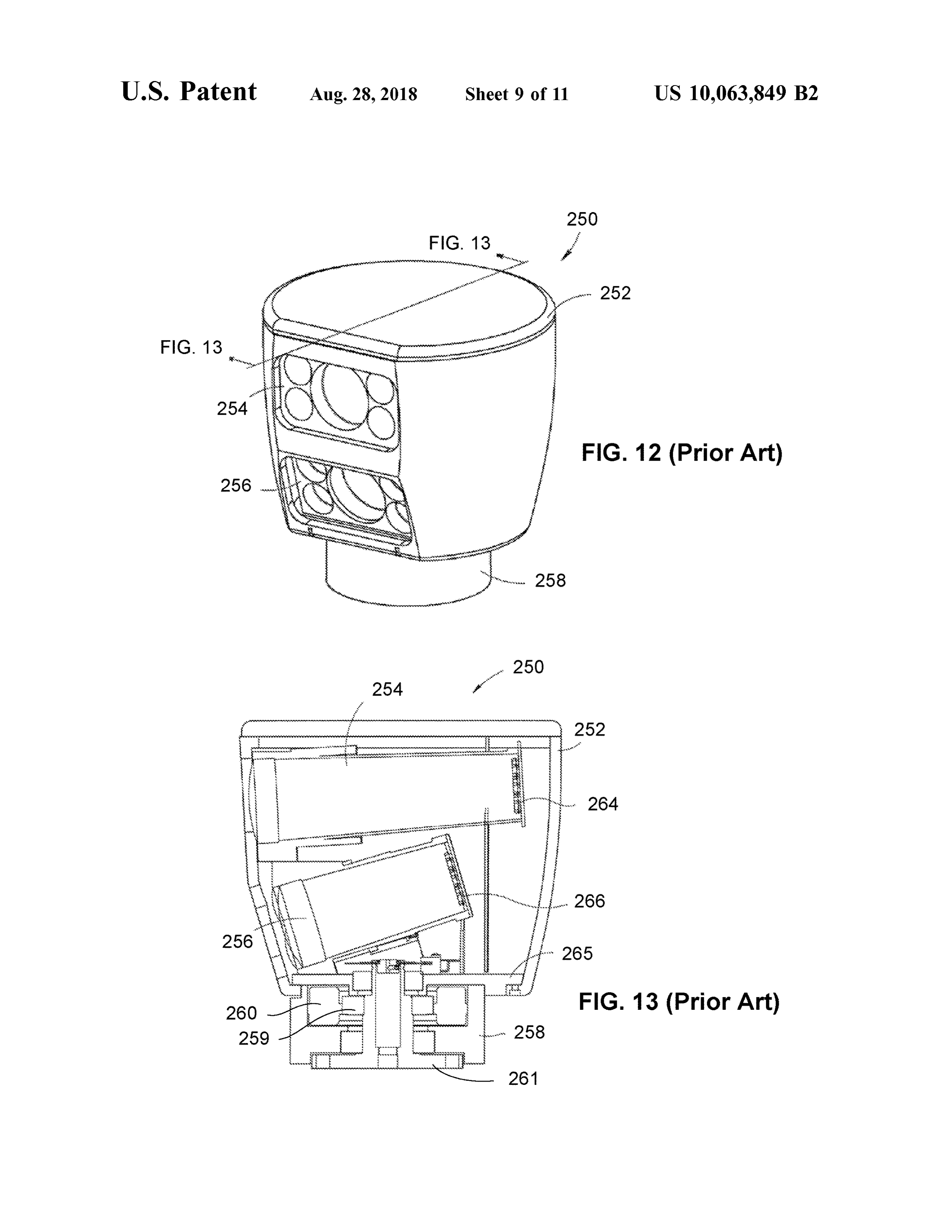
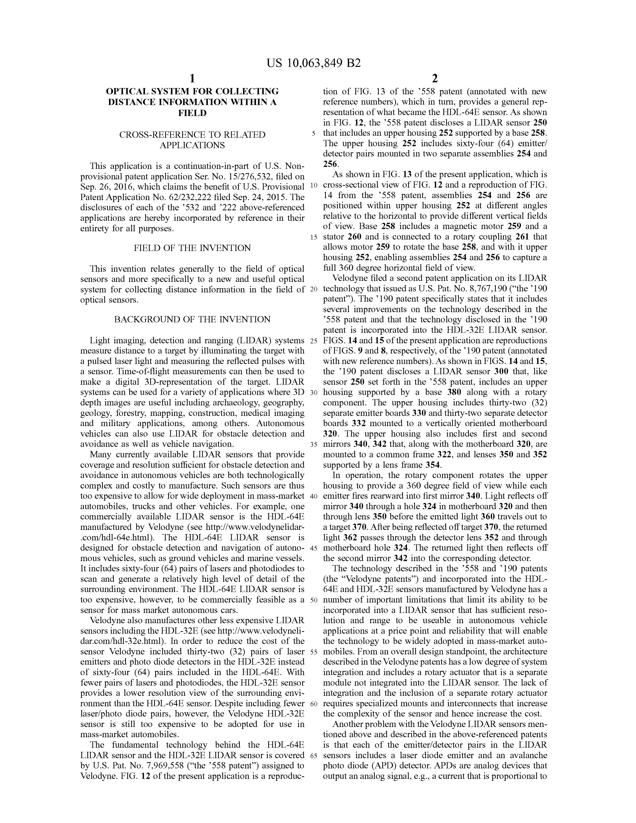
OPTICAL SYSTEM FOR COLLECTING tion of FIG . 13 of the ' 558 patent (annotated with new DISTANCE INFORMATION WITHIN A reference numbers ), which in turn , provides a general rep FIELD resentation of what became the HDL -64E sensor. As shown in FIG . 12 , the '558 patent discloses a LIDAR sensor 250
CROSS -REFERENCE TO RELATED 5 that includes an upper housing 252 supported by a base 258 . APPLICATIONS The upper housing 252 includes sixty - four (64 ) emitter/ detector pairs mounted in two separate assemblies 254 and
This application is a continuation - in - part of U . S . Non - 256 .
provisional patent application Ser. No . 15 /276 ,532 , filed on As shown in FIG . 13 of the present application , which is Sep . 26 , 2016 , which claims the benefit of U . S . Provisional 10 cross -sectional view of FIG . 12 and a reproduction of FIG . Patent Application No. 62/232 ,222 filed Sep . 24 , 2015 . The 14 from the ' 558 patent, assemblies 254 and 256 are disclosures of each of the ' 532 and ’222 above -referenced positioned within upper housing 252 at different angles applications are hereby incorporated by reference in their relative to the horizontal to provide different vertical fields entirety for all purposes. of view . Base 258 includes a magnetic motor 259 and a 15 stator 260 and is connected to a rotary coupling 261 that
FIELD OF THE INVENTION allows motor 259 to rotate the base 258 , and with it upper housing 252 , enabling assemblies 254 and 256 to capture a
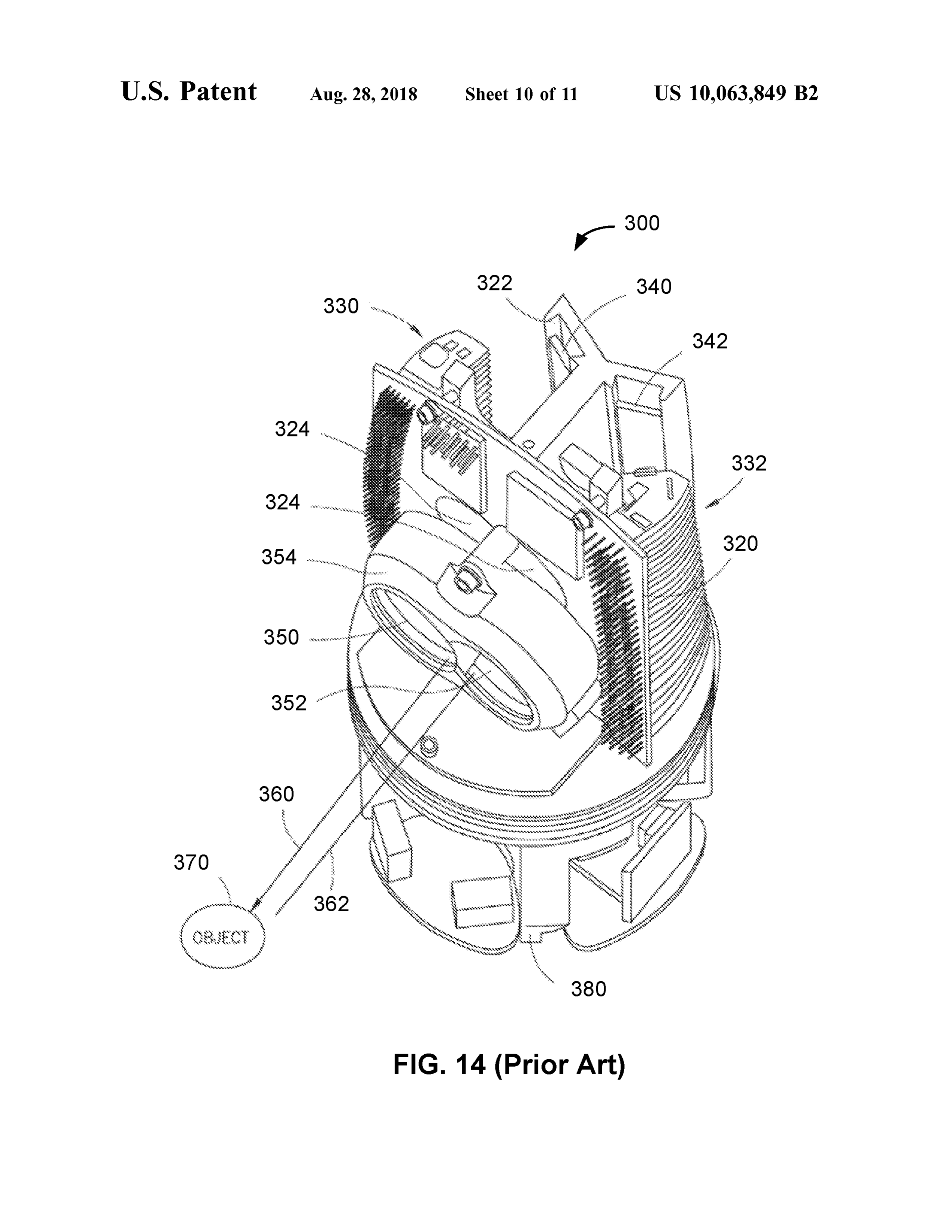
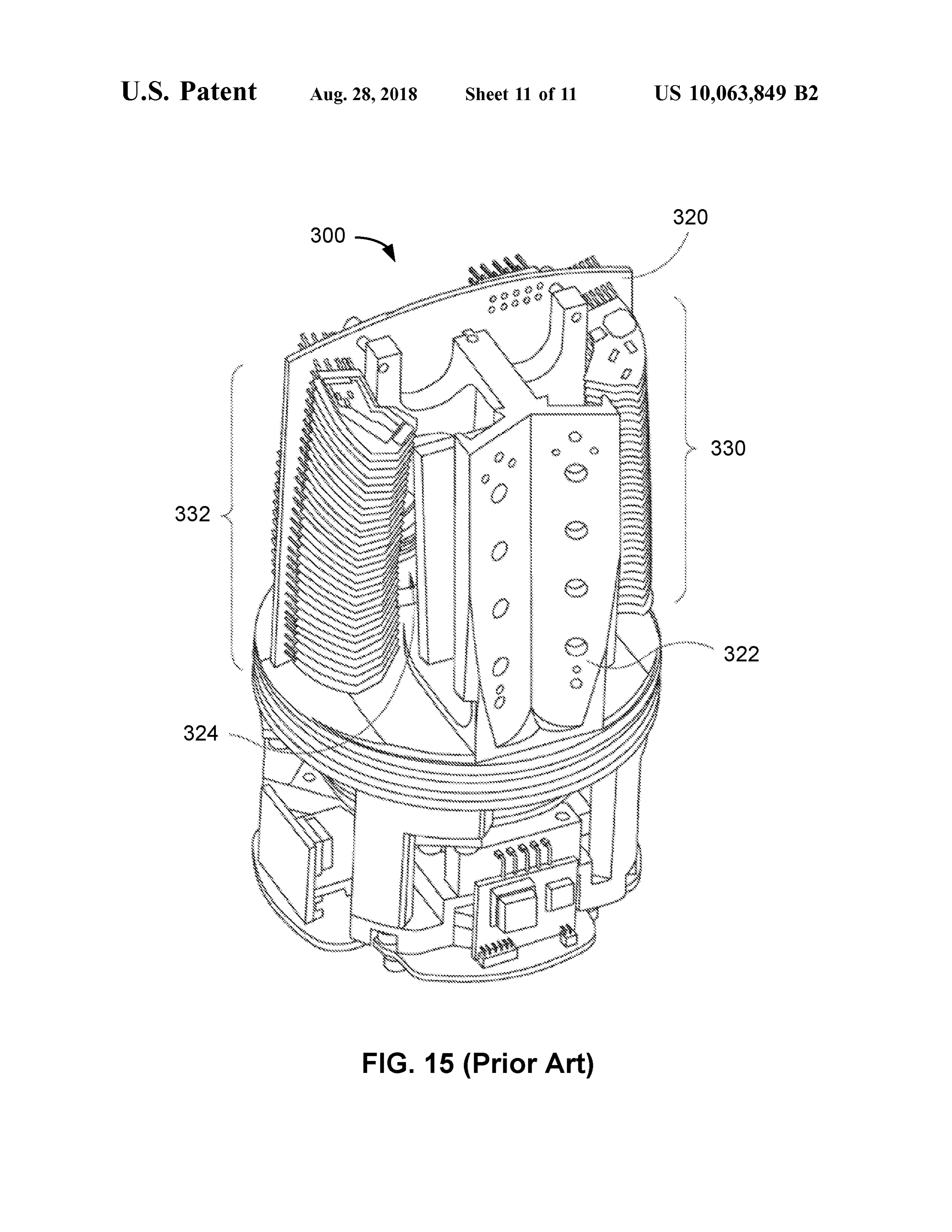
This invention relates generally to the field of optical full 360 degree horizontal field of view . sensors and more specifically to a new and useful optical Velodyne filed a second patent application on its LIDAR system for collecting distance information in the field of 20 technology that issued as U . S . Pat. No. 8 , 767, 190 (“ the ' 190 optical sensors . patent” ). The ’ 190 patent specifically states that it includes several improvements on the technology described in the
BACKGROUND OF THE INVENTION 558 patent and that the technology disclosed in the '190 patent is incorporated into the HDL -32E LIDAR sensor.
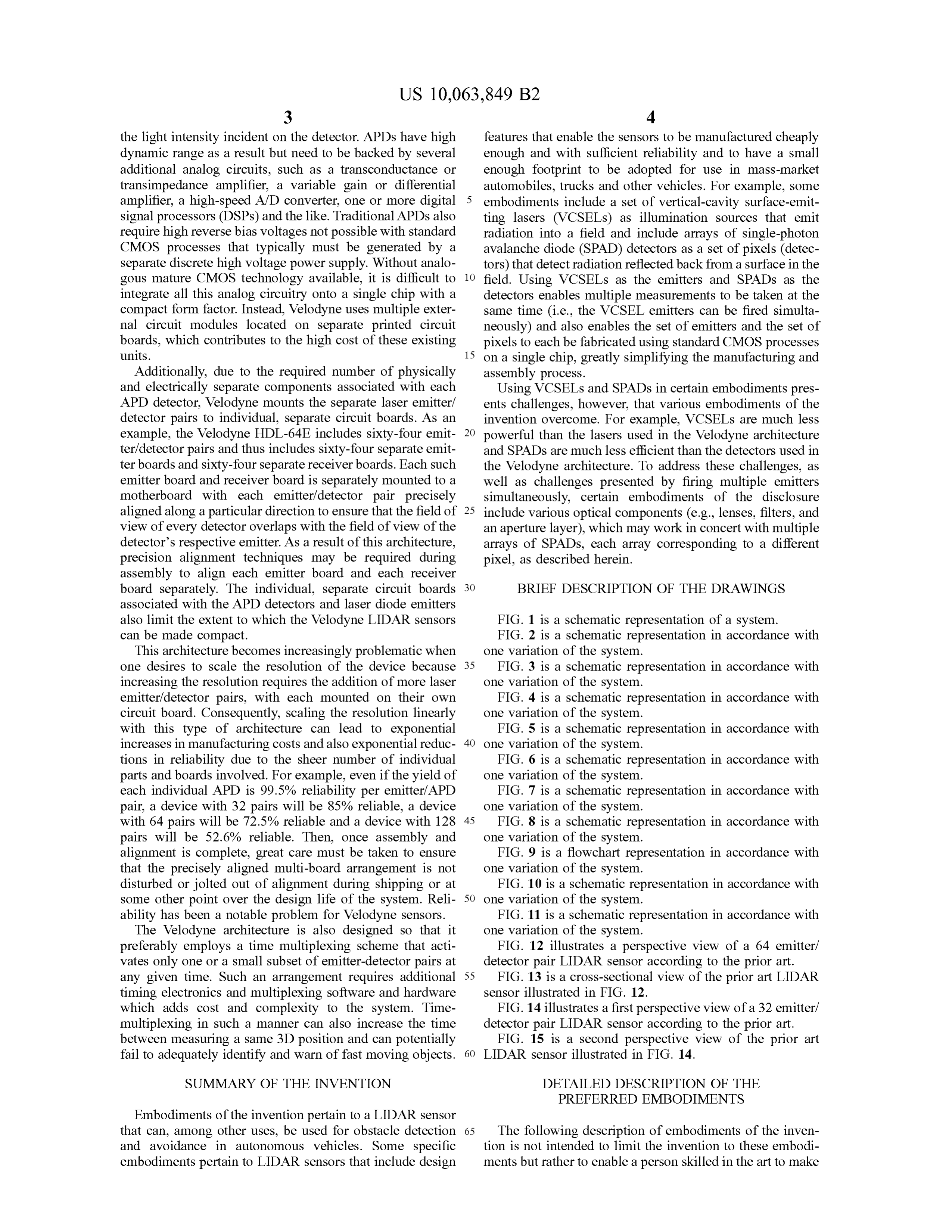
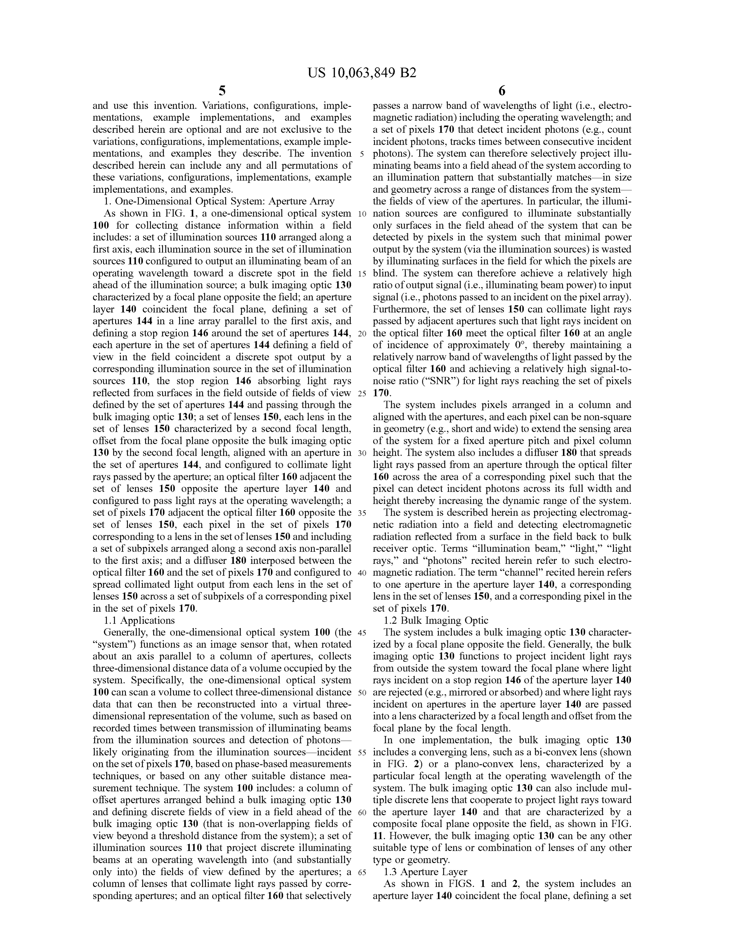
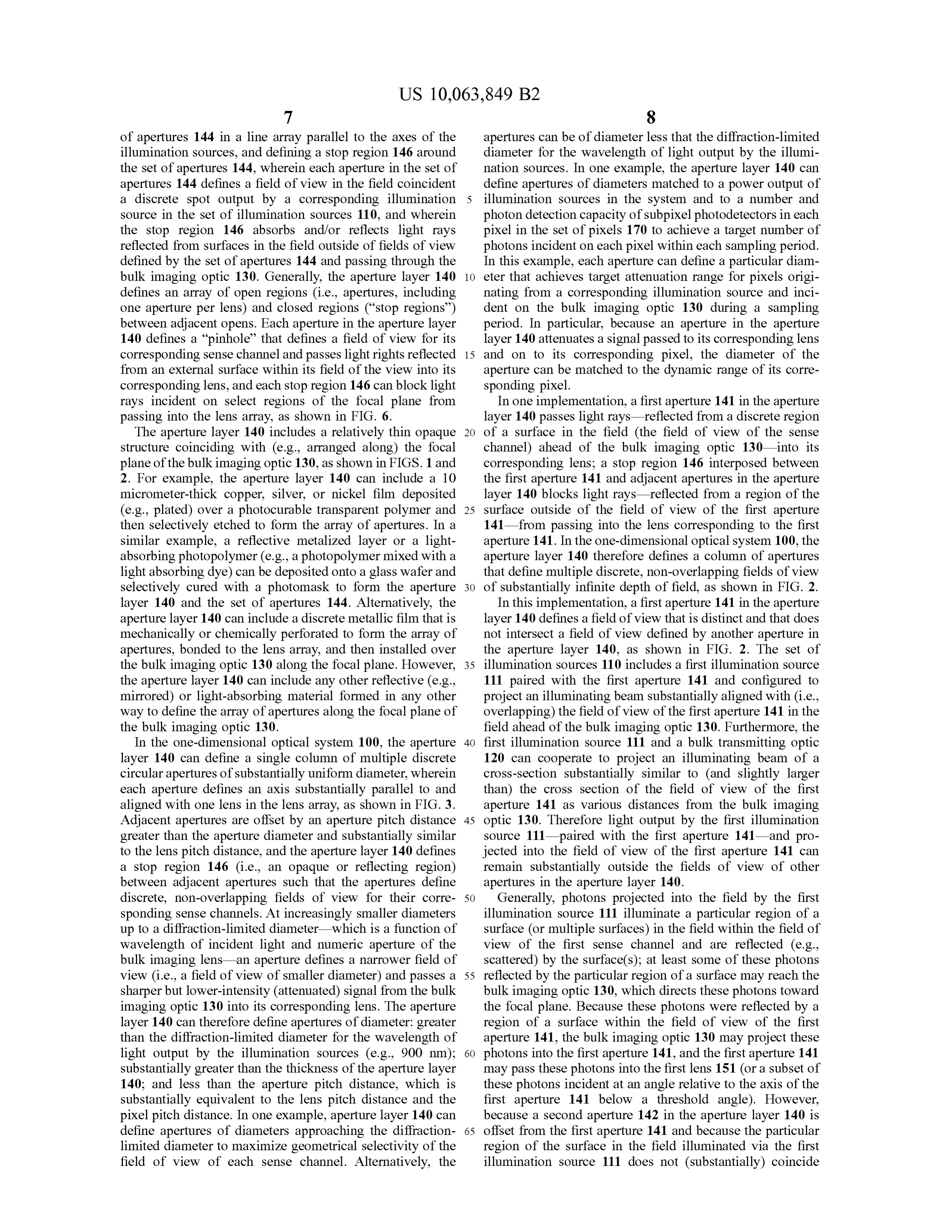
Light imaging, detection and ranging (LIDAR ) systems 25 FIGS. 14 and 15 of the present application are reproductions measure distance to a target by illuminating the target with of FIGS. 9 and 8 , respectively, of the ’ 190 patent ( annotated a pulsed laser light and measuring the reflected pulses with with new reference numbers ). As shown in FIGS. 14 and 15 , a sensor. Time-of-flight measurements can then be used to the ' 190 patent discloses a LIDAR sensor 300 that, like make a digital 3D - representation of the target. LIDAR sensor 250 set forth in the '558 patent, includes an upper systems can be used for a variety of applications where 3D 30 housing supported by a base 380 along with a rotary depth images are useful including archaeology, geography, component. The upper housing includes thirty - two (32 ) geology , forestry , mapping, construction , medical imaging separate emitter boards 330 and thirty - two separate detector and military applications, among others. Autonomous boards 332 mounted to a vertically oriented motherboard vehicles can also use LIDAR for obstacle detection and 320 . The upper housing also includes first and second avoidance as well as vehicle navigation . 35 mirrors 340 , 342 that, along with the motherboard 320 , are Many currently available LIDAR sensors that provide mounted to a common frame 322 , and lenses 350 and 352 coverage and resolution sufficient for obstacle detection and supported by a lens frame 354 . avoidance in autonomous vehicles are both technologically In operation , the rotary component rotates the upper complex and costly to manufacture. Such sensors are thus housing to provide a 360 degree field of view while each too expensive to allow for wide deployment in mass -market 40 emitter fires rearward into first mirror 340 . Light reflects off automobiles , trucks and other vehicles . For example , one mirror 340 through a hole 324 in motherboard 320 and then commercially available LIDAR sensor is the HDL -64E through lens 350 before the emitted light 360 travels out to manufactured by Velodyne (see http ://www .velodynelidar- a target 370 . After being reflected off target 370 , the returned . com /hdl -64e.html) . The HDL -64E LIDAR sensor is light 362 passes through the detector lens 352 and through designed for obstacle detection and navigation of autono - 45 motherboard hole 324 . The returned light then reflects off mous vehicles, such as ground vehicles and marine vessels . the second mirror 342 into the corresponding detector. It includes sixty - four (64) pairs of lasers and photodiodes to The technology described in the '558 and ' 190 patents scan and generate a relatively high level of detail of the (the “ Velodyne patents ” ) and incorporated into the HDL surrounding environment. The HDL -64E LIDAR sensor is 64E and HDL -32E sensors manufactured by Velodyne has a too expensive , however, to be commercially feasible as a 50 number of important limitations that limit its ability to be sensor for mass market autonomous cars . incorporated into a LIDAR sensor that has sufficient reso Velodyne also manufactures other less expensive LIDAR lution and range to be useable in autonomous vehicle sensors including the HDL - 32E ( see http ://www .velodyneli - applications at a price point and reliability that will enable dar.com /hdl- 32e .html). In order to reduce the cost of the the technology to be widely adopted in mass -market auto sensor Velodyne included thirty - two (32 ) pairs of laser 55 mobiles . From an overall design standpoint, the architecture emitters and photo diode detectors in the HDL - 32E instead described in the Velodyne patents has a low degree of system of sixty - four (64) pairs included in the HDL -64E . With integration and includes a rotary actuator that is a separate fewer pairs of lasers and photodiodes, the HDL -32E sensor module not integrated into the LIDAR sensor. The lack of provides a lower resolution view of the surrounding envi- integration and the inclusion of a separate rotary actuator ronment than the HDL -64E sensor. Despite including fewer 60 requires specialized mounts and interconnects that increase laser /photo diode pairs , however, the Velodyne HDL -32E the complexity of the sensor and hence increase the cost. sensor is still too expensive to be adopted for use in Another problem with the Velodyne LIDAR sensors men mass -market automobiles. tion tioned above and described in the above -referenced patents
The fundamental technology behind the HDL -64E is that each of the emitter/detector pairs in the LIDAR LIDAR sensor and the HDL -32E LIDAR sensor is covered 65 sensors includes a laser diode emitter and an avalanche by U . S . Pat. No . 7 , 969,558 (“ the ’ 558 patent” ) assigned to photo diode (APD ) detector. APDs are analog devices that Velodyne. FIG . 12 of the present application is a reproduc output an analog signal , e .g., a current that is proportional to
Page 16
the light intensity incident on the detector. APDs have high features that enable the sensors to be manufactured cheaply dynamic range as a result but need to be backed by several enough and with sufficient reliability and to have a small additional analog circuits, such as a transconductance or enough footprint to be adopted for use in mass -market transimpedance amplifier, a variable gain or differential automobiles, trucks and other vehicles. For example , some amplifier, a high - speed A / D converter, one or more digital 5 embodiments include a set of vertical- cavity surface - emit signal processors (DSPs) and the like. Traditional APDs also ting lasers (VCSELs ) as illumination sources that emit require high reverse bias voltages not possible with standard radiation into a field and include arrays of single -photon CMOS processes that typically must be generated by a avalanche diode (SPAD ) detectors as a set of pixels ( detec separate discrete high voltage power supply. Without analo - tors ) that detect radiation reflected back from a surface in the gous mature CMOS technology available, it is difficult to 10 field . Using VCSELs as the emitters and SPADs as the integrate all this analog circuitry onto a single chip with a detectors enables multiple measurements to be taken at the compact form factor. Instead , Velodyne uses multiple exter - same time (i.e ., the VCSEL emitters can be fired simulta nal circuit modules located on separate printed circuit neously ) and also enables the set of emitters and the set of boards, which contributes to the high cost of these existing pixels to each be fabricated using standard CMOS processes units . 15 on a single chip , greatly simplifying the manufacturing and Additionally, due to the required number of physically assembly process.
and electrically separate components associated with each Using VCSELs and SPADs in certain embodiments pres APD detector, Velodyne mounts the separate laser emitter / ents challenges, however, that various embodiments of the detector pairs to individual, separate circuit boards . As an invention overcome. For example, VCSELs are much less example , the Velodyne HDL -64E includes sixty - four emit- 20 powerful than the lasers used in the Velodyne architecture ter/detector pairs and thus includes sixty - four separate emit and SPADs are much less efficient than the detectors used in ter boards and sixty - four separate receiver boards. Each such the Velodyne architecture. To address these challenges, as emitter board and receiver board is separately mounted to a well as challenges presented by firing multiple emitters motherboard with each emitter/ detector pair precisely simultaneously, certain embodiments of the disclosure aligned along a particular direction to ensure that the field of 25 include various optical components (e .g ., lenses, filters, and view of every detector overlaps with the field of view of the an aperture layer ), which may work in concert with multiple detector's respective emitter. As a result of this architecture , arrays of SPADs, each array corresponding to a different precision alignment techniques may be required during pixel, as described herein .
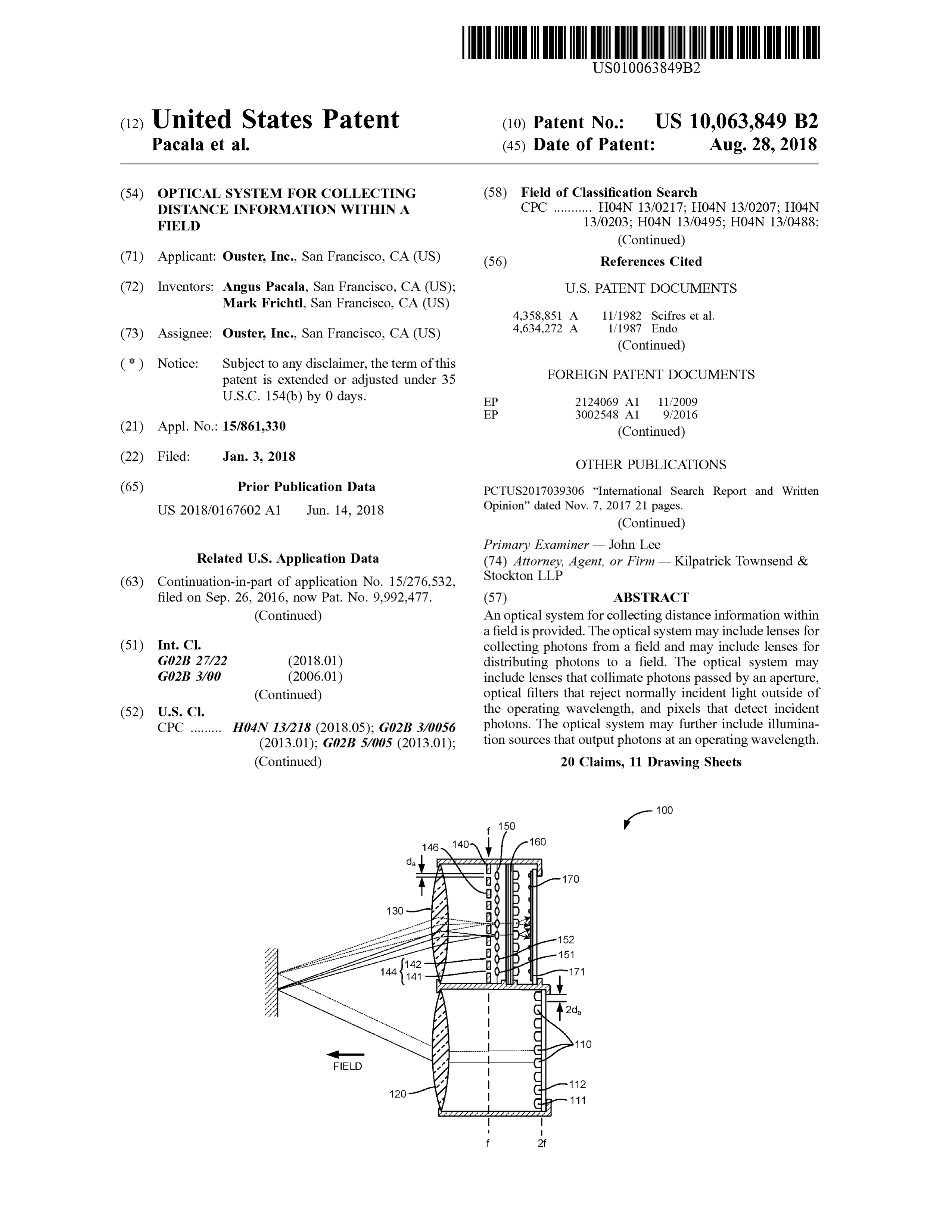
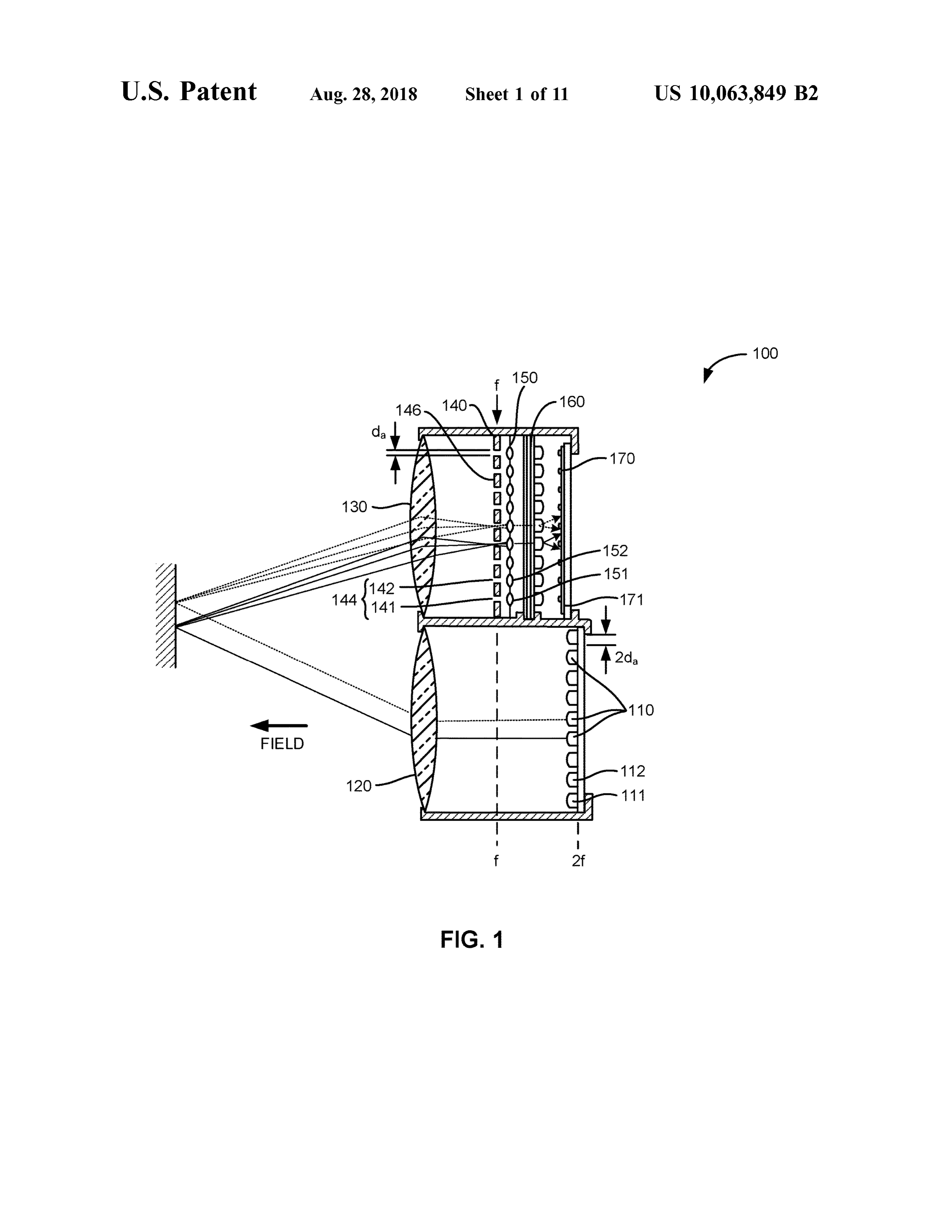
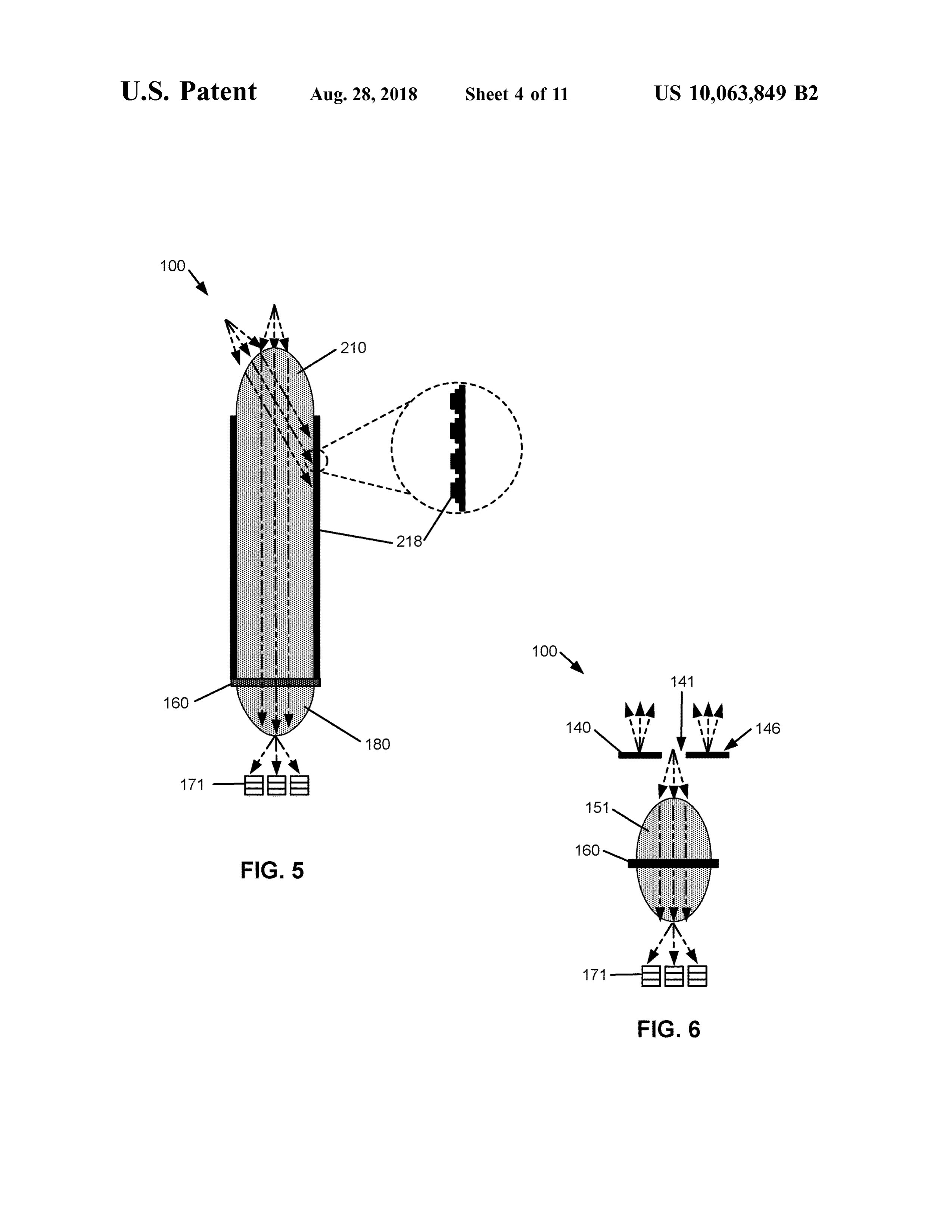
assembly to align each emitter board and each receiver board separately . The individual, separate circuit boards 30 BRIEF DESCRIPTION OF THE DRAWINGS associated with the APD detectors and laser diode emitters also limit the extent to which the Velodyne LIDAR sensors FIG . 1 is a schematic representation of a system . can be made compact . FIG . 2 is a schematic representation in accordance with This architecture becomes increasingly problematic when one variation of the system .
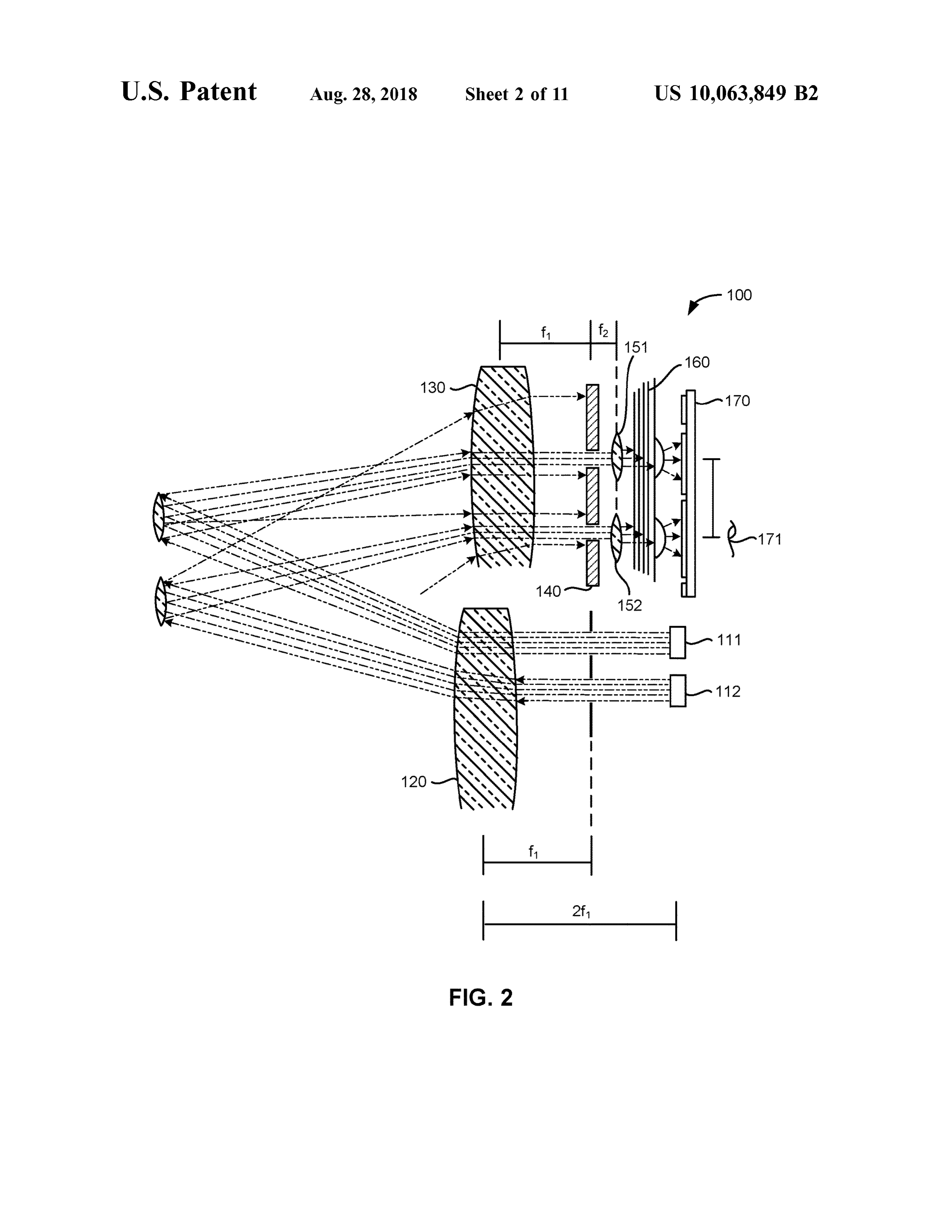
one desires to scale the resolution of the device because 35 FIG . 3 is a schematic representation in accordance with increasing the resolution requires the addition ofmore laser o ne variation of the system .
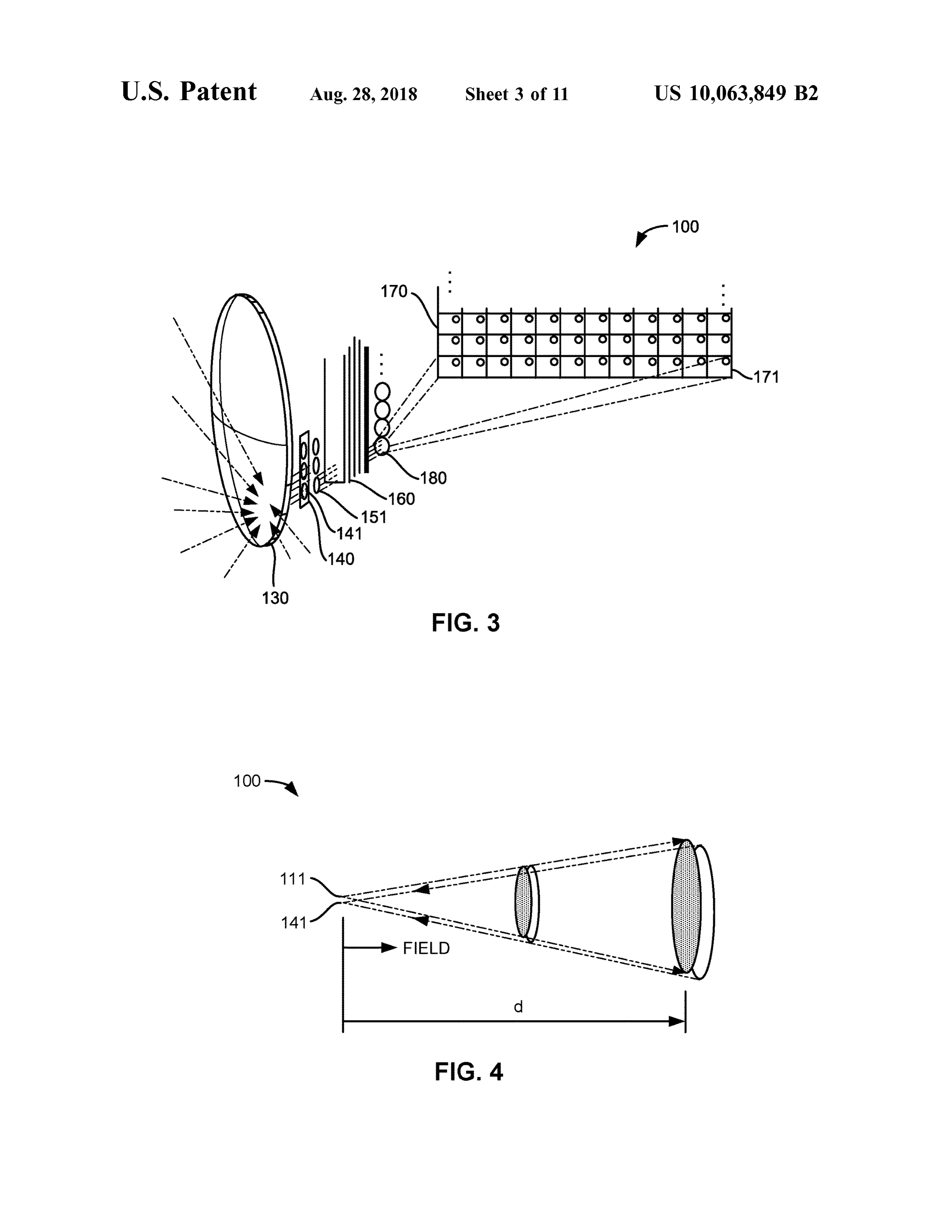
emitter/detector pairs, with each mounted on their own FIG . 4 is a schematic representation in accordance with circuit board . Consequently , scaling the resolution linearly one variation of the system .
with this type of architecture can lead to exponential FIG . 5 is a schematic representation in accordance with increases in manufacturing costs and also exponential reduc - 40 one variation of the system .
tions in reliability due to the sheer number of individual FIG . 6 is a schematic representation in accordance with parts and boards involved . For example, even if the yield of one variation of the system .
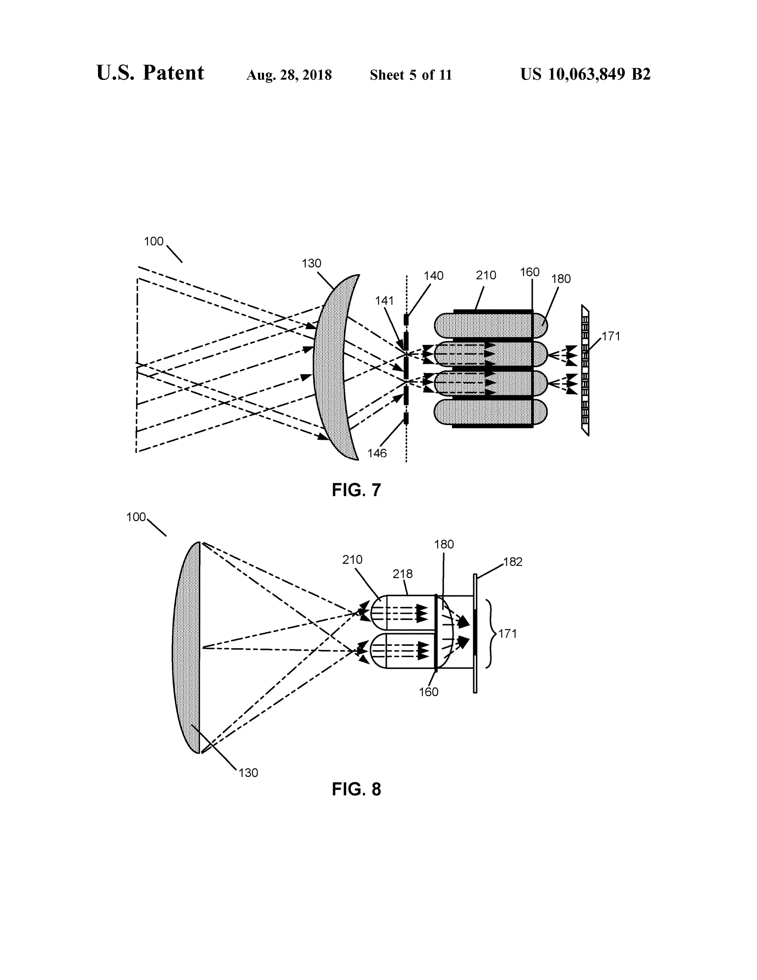
each individual APD is 99 . 5 % reliability per emitter/ APD FIG . 7 is a schematic representation in accordance with pair , a device with 32 pairs will be 85 % reliable , a device one variation of the system .
with 64 pairs will be 72.5 % reliable and a device with 128 45 FIG . 8 is a schematic representation in accordance with pairs will be 52 .6 % reliable. Then , once assembly and one variation of the system .
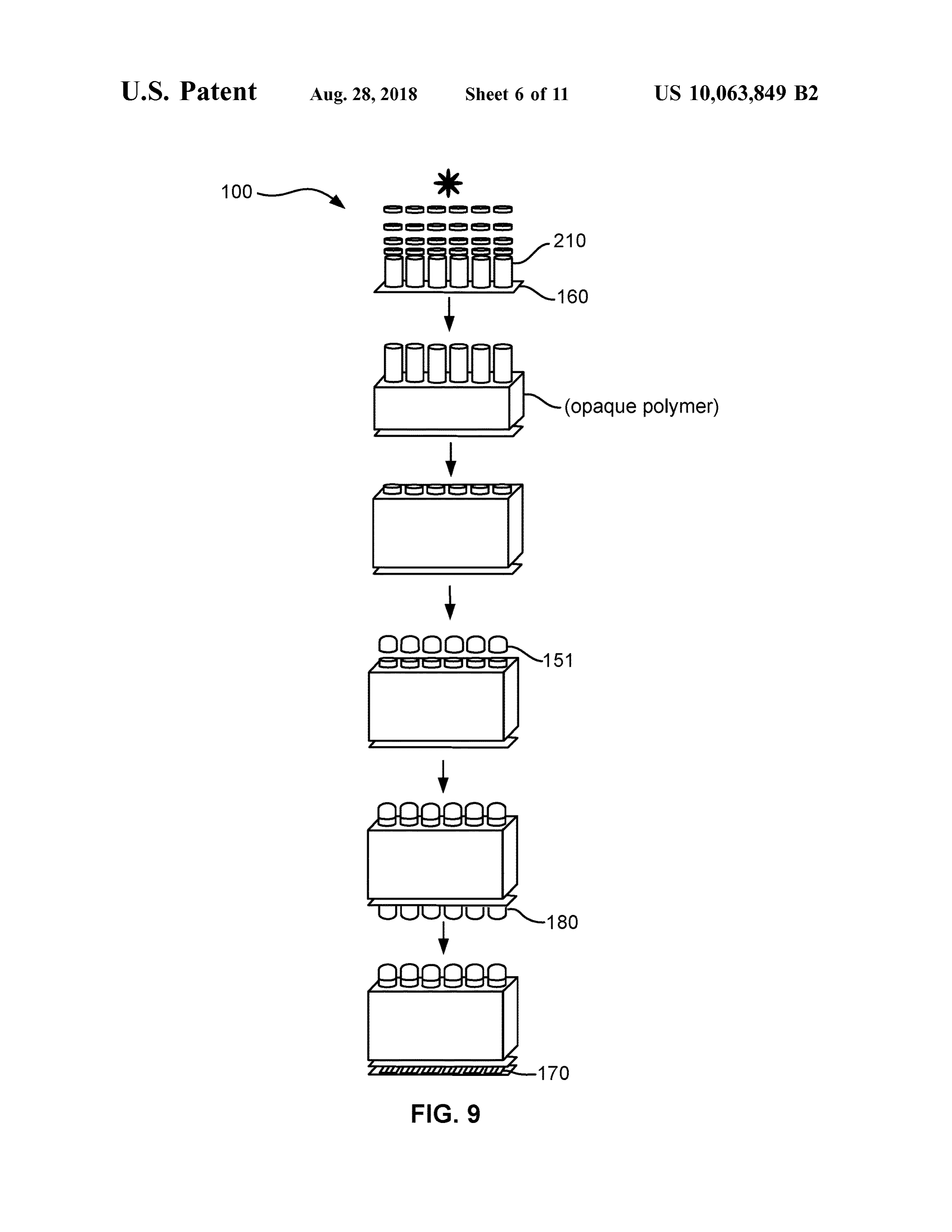
alignment is complete , great care must be taken to ensure FIG . 9 is a flowchart representation in accordance with that the precisely aligned multi-board arrangement is not one variation of the system .
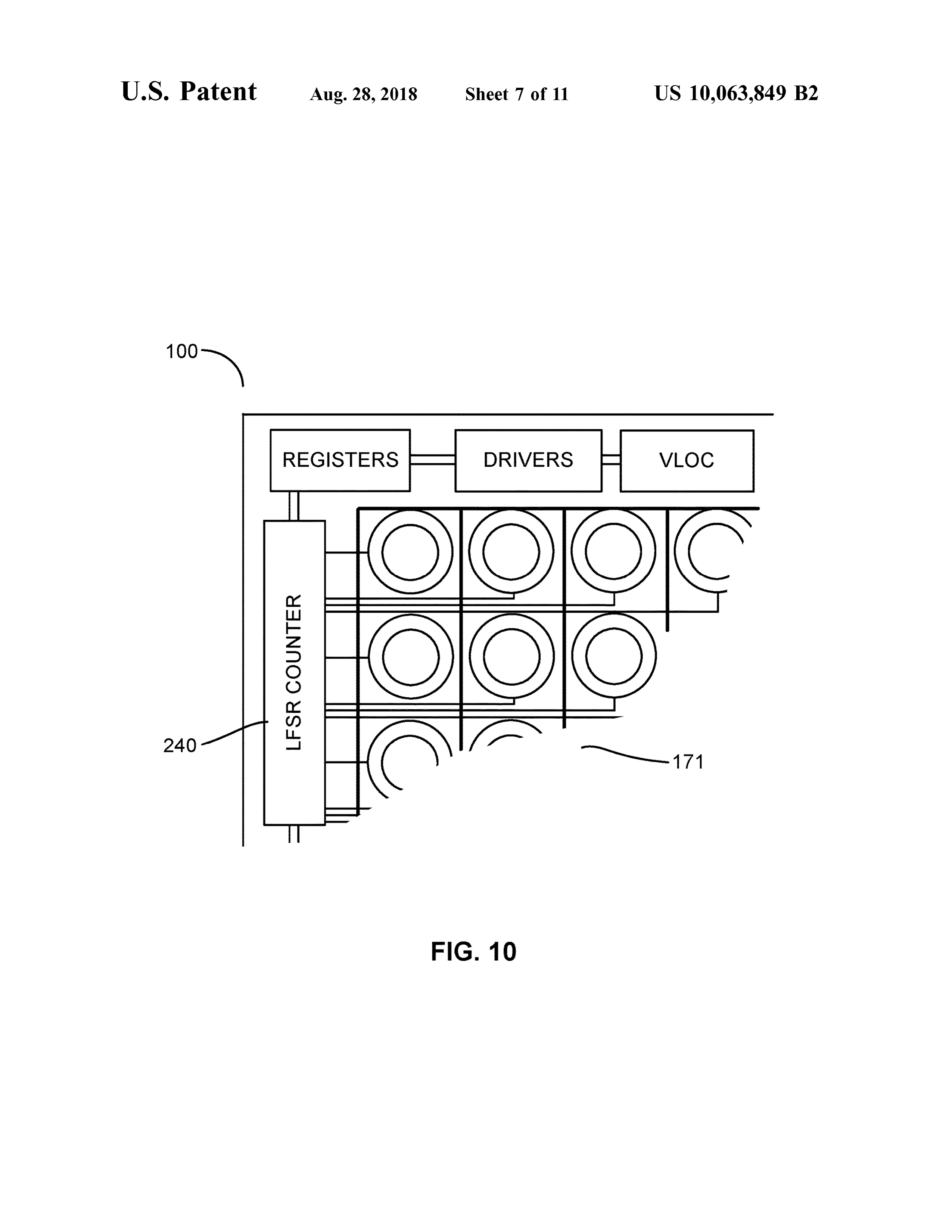
disturbed or jolted out of alignment during shipping or at FIG . 10 is a schematic representation in accordance with some other point over the design life of the system . Reli - 50 one variation of the system .
ability has been a notable problem for Velodyne sensors . FIG . 11 is a schematic representation in accordance with The Velodyne architecture is also designed so that it one variation of the system .
preferably employs a time multiplexing scheme that acti- FIG . 12 illustrates a perspective view of a 64 emitter / vates only one or a small subset of emitter -detector pairs at detector pair LIDAR sensor according to the prior art. any given time. Such an arrangement requires additional 55 FIG . 13 is a cross - sectional view of the prior art LIDAR timing electronics and multiplexing software and hardware sensor illustrated in FIG . 12 .
which adds cost and complexity to the system . Time- FIG . 14 illustrates a first perspective view of a 32 emitter/ multiplexing in such a manner can also increase the time detector pair LIDAR sensor according to the prior art. between measuring a same 3D position and can potentially FIG . 15 is a second perspective view of the prior art fail to adequately identify and warn of fast moving objects. 60 LIDAR sensor illustrated in FIG . 14 . SUMMARY OF THE INVENTION DETAILED DESCRIPTION OF THE
PREFERRED EMBODIMENTS
Embodiments of the invention pertain to a LIDAR sensor that can , among other uses , be used for obstacle detection 65 The following description of embodiments of the inven and avoidance in autonomous vehicles. Some specific tion is not intended to limit the invention to these embodi embodiments pertain to LIDAR sensors that include design ments but rather to enable a person skilled in the art to make
Page 17
and use this invention . Variations, configurations, imple passes a narrow band of wavelengths of light (i.e., electro mentations, example implementations, and examples magnetic radiation , including the operating wavelength ; and described herein are optional and are not exclusive to the a set of pixels 170 that detect incident photons ( e . g ., count variations , configurations, implementations, example imple - incident photons, tracks times between consecutive incident mentations, and examples they describe . The invention 5 photons ). The system can therefore selectively project illu described herein can include any and all permutations of minating beams into a field ahead of the system according to these variations, configurations, implementations, example an illumination pattern that substantially matches — in size implementations, and examples . and geometry across a range of distances from the system 1. One-Dimensional Optical System : Aperture Array the fields of view of the apertures. In particular, the illumi As shown in FIG . 1 , a one- dimensional optical system 10 nation sources are configured to illuminate substantially 100 for collecting distance information within a field only surfaces in the field ahead of the system that can be includes : a set of illumination sources 110 arranged along a detected by pixels in the system such that minimal power first axis , each illumination source in the set of illumination output by the system ( via the illumination sources ) is wasted sources 110 configured to output an illuminating beam of an by illuminating surfaces in the field for which the pixels are operating wavelength toward a discrete spot in the field 15 blind . The system can therefore achieve a relatively high ahead of the illumination source ; a bulk imaging optic 130 ratio of output signal (i. e., illuminating beam power ) to input characterized by a focal plane opposite the field ; an aperture signal ( i.e ., photons passed to an incident on the pixel array ) . layer 140 coincident the focal plane , defining a set of Furthermore , the set of lenses 150 can collimate light rays apertures 144 in a line array parallel to the first axis, and passed by adjacent apertures such that light rays incident on defining a stop region 146 around the set of apertures 144 , 20 the optical filter 160 meet the optical filter 160 at an angle each aperture in the set of apertures 144 defining a field of of incidence of approximately 0°, thereby maintaining a view in the field coincident a discrete spot output by a relatively narrow band ofwavelengths of light passed by the corresponding illumination source in the set of illumination optical filter 160 and achieving a relatively high signal- to sources 110 , the stop region 146 absorbing light rays noise ratio (“ SNR ” ) for light rays reaching the set of pixels reflected from surfaces in the field outside of fields of view 25 170 .
defined by the set of apertures 144 and passing through the The system includes pixels arranged in a column and bulk imaging optic 130 ; a set of lenses 150 , each lens in the aligned with the apertures , and each pixel can be non - square set of lenses 150 characterized by a second focal length , in geometry (e . g ., short and wide) to extend the sensing area offset from the focal plane opposite the bulk imaging optic of the system for a fixed aperture pitch and pixel column 130 by the second focal length , aligned with an aperture in 30 height. The system also includes a diffuser 180 that spreads the set of apertures 144 , and configured to collimate light light rays passed from an aperture through the optical filter rays passed by the aperture ; an optical filter 160 adjacent the 160 across the area of a corresponding pixel such that the set of lenses 150 opposite the aperture layer 140 and pixel can detect incident photons across its full width and configured to pass light rays at the operating wavelength ; a height thereby increasing the dynamic range of the system . set of pixels 170 adjacent the optical filter 160 opposite the 35 The system is described herein as projecting electromag set of lenses 150, each pixel in the set of pixels 170 netic radiation into a field and detecting electromagnetic corresponding to a lens in the set oflenses 150 and including radiation reflected from a surface in the field back to bulk a set of subpixels arranged along a second axis non -parallel receiver optic . Terms “ illumination beam ," " light," " light to the first axis ; and a diffuser 180 interposed between the rays," and " photons ” recited herein refer to such electro optical filter 160 and the set of pixels 170 and configured to 40 magnetic radiation . The term " channel” recited herein refers spread collimated light output from each lens in the set of to one aperture in the aperture layer 140, a corresponding lenses 150 across a set of subpixels of a corresponding pixel l ens in the set of lenses 150 , and a corresponding pixel in the in the set of pixels 170 . set of pixels 170.
1 . 1 Applications 1. 2 Bulk Imaging Optic
Generally , the one- dimensional optical system 100 ( the 45 The system includes a bulk imaging optic 130 character " system ” ) functions as an image sensor that, when rotated ized by a focal plane opposite the field . Generally, the bulk about an axis parallel to a column of apertures , collects imaging optic 130 functions to project incident light rays three -dimensional distance data of a volume occupied by the from outside the system toward the focal plane where light system . Specifically , the one -dimensional optical system rays incident on a stop region 146 of the aperture layer 140 100 can scan a volume to collect three -dimensional distance 50 are rejected ( e . g ., mirrored or absorbed ) and where light rays data that can then be reconstructed into a virtual three - incident on apertures in the aperture layer 140 are passed dimensional representation of the volume, such as based on into a lens characterized by a focal length and offset from the recorded times between transmission of illuminating beams focal plane by the focal length .
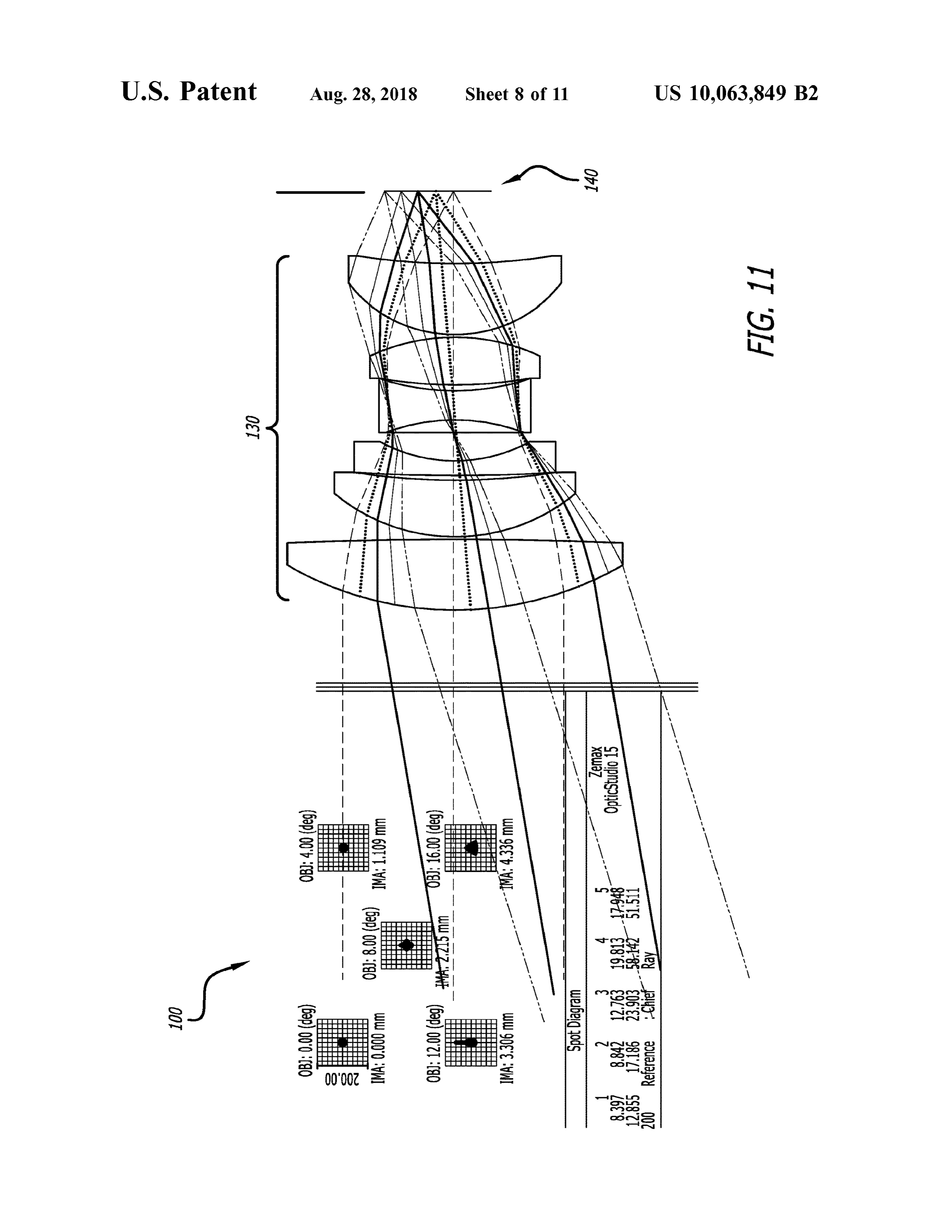
from the illumination sources and detection of photons In one implementation , the bulk imaging optic 130 likely originating from the illumination sources incident 55 includes a converging lens, such as a bi-convex lens ( shown on the set of pixels 170 , based on phase -based measurements in FIG . 2 ) or a plano - convex lens, characterized by a techniques, or based on any other suitable distance mea particular focal length at the operating wavelength of the surement technique. The system 100 includes : a column of system . The bulk imaging optic 130 can also include mul offset apertures arranged behind a bulk imaging optic 130 tiple discrete lens that cooperate to project light rays toward and defining discrete fields of view in a field ahead of the 60 the aperture layer 140 and that are characterized by a bulk imaging optic 130 (that is non -overlapping fields of composite focal plane opposite the field , as shown in FIG . view beyond a threshold distance from the system ); a set of 11 . However , the bulk imaging optic 130 can be any other illumination sources 110 that project discrete illuminating suitable type of lens or combination of lenses of any other beams at an operating wavelength into ( and substantially type or geometry .
only into ) the fields of view defined by the apertures ; a 65 1.3 Aperture Layer column of lenses that collimate light rays passed by corre As shown in FIGS . 1 and 2 , the system includes an sponding apertures; and an optical filter 160 that selectively aperture layer 140 coincident the focal plane, defining a set
Page 18
of apertures 144 in a line array parallel to the axes of the apertures can be of diameter less that the diffraction -limited illumination sources, and defining a stop region 146 around diameter for the wavelength of light output by the illumi the set of apertures 144 , wherein each aperture in the set of nation sources . In one example , the aperture layer 140 can apertures 144 defines a field of view in the field coincident define apertures of diameters matched to a power output of a discrete spot output by a corresponding illumination 5 illumination sources in the system and to a number and source in the set of illumination sources 110 , and wherein photon detection capacity of subpixel photodetectors in each the stop region 146 absorbs and/ or reflects light rays pixel in the set of pixels 170 to achieve a target number of reflected from surfaces in the field outside of fields of view photons incident on each pixel within each sampling period . defined by the set of apertures 144 and passing through the In this example, each aperture can define a particular diam bulk imaging optic 130 . Generally , the aperture layer 140 10 eter that achieves target attenuation range for pixels origi defines an array of open regions (i.e ., apertures, including nating from a corresponding illumination source and inci one aperture per lens) and closed regions (“ stop regions” ) dent on the bulk imaging optic 130 during a sampling between adjacent opens. Each aperture in the aperture layer period . In particular , because an aperture in the aperture 140 defines a " pinhole ” that defines a field of view for its layer 140 attenuates a signal passed to its corresponding lens corresponding sense channel and passes light rights reflected 15 and on to its corresponding pixel, the diameter of the from an external surface within its field of the view into its aperture can be matched to the dynamic range of its corre corresponding lens, and each stop region 146 can block light sponding pixel.
rays incident on select regions of the focal plane from In one implementation , a first aperture 141 in the aperture passing into the lens array , as shown in FIG . 6 . layer 140 passes light rays — reflected from a discrete region The aperture layer 140 includes a relatively thin opaque 20 of a surface in the field (the field of view of the sense structure coinciding with ( e. g ., arranged along ) the focal channel) ahead of the bulk imaging optic 130 — into its plane of the bulk imaging optic 130 , as shown in FIGS. 1 and corresponding lens; a stop region 146 interposed between 2 . For example, the aperture layer 140 can include a 10 the first aperture 141 and adjacent apertures in the aperture micrometer -thick copper , silver, or nickel film deposited layer 140 blocks light rays - reflected from a region of the ( e . g ., plated ) over a photocurable transparent polymer and 25 surface outside of the field of view of the first aperture then selectively etched to form the array of apertures. In a 141 — from passing into the lens corresponding to the first similar example , a reflective metalized layer or a light- aperture 141. In the one- dimensional optical system 100 , the absorbing photopolymer ( e . g ., a photopolymer mixed with a aperture layer 140 therefore defines a column of apertures light absorbing dye ) can be deposited onto a glass wafer and that define multiple discrete , non -overlapping fields of view selectively cured with a photomask to form the aperture 30 of substantially infinite depth of field , as shown in FIG . 2 . layer 140 and the set of apertures 144 . Alternatively , the In this implementation , a first aperture 141 in the aperture aperture layer 140 can include a discrete metallic film that is layer 140 defines a field of view that is distinct and that does mechanically or chemically perforated to form the array of not intersect a field of view defined by another aperture in apertures , bonded to the lens array, and then installed over the aperture layer 140 , as shown in FIG . 2 . The set of the bulk imaging optic 130 along the focal plane . However, 35 illumination sources 110 includes a first illumination source the aperture layer 140 can include any other reflective ( e . g ., 111 paired with the first aperture 141 and configured to mirrored ) or light-absorbing material formed in any other project an illuminating beam substantially aligned with (i.e., way to define the array of apertures along the focal plane of overlapping ) the field of view of the first aperture 141 in the the bulk imaging optic 130 . field ahead of the bulk imaging optic 130 . Furthermore , the In the one - dimensional optical system 100 , the aperture 40 first illumination source 111 and a bulk transmitting optic layer 140 can define a single column of multiple discrete 120 can cooperate to project an illuminating beam of a circular apertures of substantially uniform diameter, wherein cross -section substantially similar to (and slightly larger each aperture defines an axis substantially parallel to and than ) the cross section of the field of view of the first aligned with one lens in the lens array , as shown in FIG . 3. aperture 141 as various distances from the bulk imaging Adjacent apertures are offset by an aperture pitch distance 45 optic 130 . Therefore light output by the first illumination greater than the aperture diameter and substantially similar source 111 — paired with the first aperture 141 — and pro to the lens pitch distance, and the aperture layer 140 defines jected into the field of view of the first aperture 141 can a stop region 146 (i.e ., an opaque or reflecting region ) remain substantially outside the fields of view of other between adjacent apertures such that the apertures define apertures in the aperture layer 140 . discrete, non -overlapping fields of view for their corre - 50 Generally, photons projected into the field by the first sponding sense channels . At increasingly smaller diameters illumination source 111 illuminate a particular region of a up to a diffraction - limited diameter — which is a function of surface (or multiple surfaces ) in the field within the field of wavelength of incident light and numeric aperture of the view of the first sense channel and are reflected (e . g ., bulk imaging lens— an aperture defines a narrower field of scattered ) by the surface (s ); at least some of these photons view (i.e ., a field of view of smaller diameter ) and passes a 55 reflected by the particular region of a surface may reach the sharper but lower -intensity (attenuated ) signal from the bulk bulk imaging optic 130 , which directs these photons toward imaging optic 130 into its corresponding lens. The aperture the focal plane. Because these photons were reflected by a layer 140 can therefore define apertures of diameter : greater region of a surface within the field of view of the first than the diffraction -limited diameter for the wavelength of aperture 141, the bulk imaging optic 130 may project these light output by the illumination sources (e . g ., 900 nm ); 60 photons into the first aperture 141, and the first aperture 141 substantially greater than the thickness of the aperture layer may pass these photons into the first lens 151 (or a subset of 140; and less than the aperture pitch distance , which is these photons incident at an angle relative to the axis of the substantially equivalent to the lens pitch distance and the first aperture 141 below a threshold angle ). However, pixel pitch distance . In one example, aperture layer 140 can because a second aperture 142 in the aperture layer 140 is define apertures of diameters approaching the diffraction - 65 offset from the first aperture 141 and because the particular limited diameter to maximize geometrical selectivity of the region of the surface in the field illuminated via the first field of view of each sense channel. Alternatively , the illumination source 111 does not (substantially ) coincide
Page 19
with the field of view of the second aperture 142 , photons 1.4 Lens Array reflected by the particular region of the surface and reaching The system includes a set of lenses 150 , wherein each lens the bulk imaging optic 130 are projected into the second in the set of lenses 150 is characterized by a second focal aperture 142 and passed to a second lens 152 behind the length , is offset from the focal plane opposite the bulk second aperture 142, and vice versa , as shown in FIG . 2 . 5 imaging optic 130 by the second focal length , is aligned with Furthermore, a stop region 146 between the first and second a corresponding aperture in the set of apertures 144 , and is apertures 142 can block photons directed toward the focal configured to collimate light rays passed by the correspond plane between the first and second apertures 142 reflected by ing aperture . Generally , a lens in the set of lenses 150 the bulk imaging optic 130 , thereby reducing crosstalk functions to collimate lights rays passed by its correspond between the first and second sense channels . ing aperture and to pass these collimated light rays into the For a first aperture 141 in the aperture layer 140 paired optical filter 160.
with a first illumination source 111 in the set of illumination In the one -dimensional optical system 100, the lenses are sources 110 , the first aperture 141 in the aperture layer 140 arranged in a single column, and adjacent lenses are offset defines a first field of view and passes into the first lens 1 by a uniform lens pitch distance ( i.e ., a center -to -center 151 - incident light rays originating at or reflected from a distance between adjacent pixels ), as shown in FIG . 3 . The surface in the field coinciding with the first field of view . set of lenses 150 is interposed between the aperture layer and Because the first illumination source 111 projects an illumi the optical filter 160 . In particular, each lens can include a nating beam that is substantially coincident (and substan converging lens characterized by a second focal length and tially the same size as or minimally larger than ) the field of 20 can be offset from the focal plane of the bulk imaging optic 130 — opposite the bulk imaging optic 130 — by the second view defined by the first aperture 141 (as shown in FIG . 4 ), focal length to preserve the aperture of the bulk imaging a signal passed into the first lens 151 by the first aperture 141 optic 130 in the aperture layer 140 can exhibit a relatively high ratio optic 130 and to collimate light incident on the bulk imaging and passed by a corresponding aperture. Each lens of light rays originating from the first illumination source in the set of lens can be characterized by a relatively short 111 to light rays originating from other illumination sources 25 focal length (i.e ., less than a focal length of the bulk imaging in the system . Generally , because various illumination optic 130 ) and a relatively large marginal ray angle ( e . g ., a sources in the system may output illuminating beams at relatively high numeric aperture lens) such that the lens can different frequencies, duty cycles, and /or power levels , etc . capture highly -angled light rays projected toward the lens by at a particular time during operation , light rays passed from the extent of the bulk imaging optic 130 . That is, each lens the bulk imaging optic 130 into a first pixel 171 in the set of > in the set of lens can be characterized by a ray cone pixels 170 but originating from an illumination source other substantially matched to a ray cone of the bulk imaging optic than the first illumination source 111 paired with the first 130 .
pixel 171 constitute noise at the first pixel 171. Though the Lenses in the set of lenses 150 can be substantially relatively small diameters of apertures in the aperture layer as similar. A lens in the set of lenses 150 is configured to 140 may attenuate a total light signal passed from the bulk collimate light rays focused into its corresponding aperture imaging optic 130 into the set of lenses 150 , each aperture by thebulk imaging optic 130 . For example , a lens in the set in the aperture layer 140 may pass a relatively high propor- of lenses 150 can include a bi- convex or plano -convex lens tion of photons originating from its corresponding illumi characterized by a focal length selected based on the size nation source than from other illumination sources in the the 404 ating (e.g ., diameter ) of its corresponding aperture and the oper wavelength of the system . In this example , the focal system ; that is , due to the geometry of a particular aperture length and its corresponding illumination source, a particular aper according (f) of a lens in the set of lenses 150 can be calculated ture may pass a signal exhibiting a relatively high SNR to its to the formula :
corresponding lens and thus into its corresponding pixel.
Furthermore , at smaller aperture diameters in the aperture 45 d2 layer 140 — and therefore smaller fields of view of corre f= a sponding channels — the system can pass less noise from solar radiation or other ambient light sources to the set of pixels 170 . where d is the diameter of the corresponding aperture in the In one variation , the system includes a second aperture 50 aperture layer and à is the operating wavelength of light layer interposed between the lens array and the optical filter output by the illumination source ( e. g ., 900 nm ). The geom 160 , wherein the second aperture layer defines a second set etry of a lens in the set of lenses 150 can therefore be of apertures 144 , each aligned with a corresponding lens in matched to the geometry of a corresponding aperture in the the set of lenses 150 , as described above. In this variation , aperture layer such that the lens passes a substantially sharp an aperture in the second aperture layer 140 can absorb or 55 image of light rays — at or near the operating wavelength — reflect errant light rays passed by a corresponding lens , as into the optical filter 160 and thus on to the pixel array . described above , to further reduce crosstalk between chan - However, the set of lenses 150 can include lenses of any nels , thereby improving SNR within the system . Similarly, other geometry and arranged in any other way adjacent the the system can additionally or alternatively include a third aperture layer.
aperture layer interposed between the optical filter 160 and 60 1.5 Optical Filter the diffuser(s ) 180, wherein the third aperture layer defines As shown in FIG . 3 , the system includes an optical filter a third set of apertures 144 , each aligned with a correspond- 160 adjacent the set of lenses 150 opposite the aperture layer ing lens in the set of lenses 150, as described above . In this and configured to pass light rays at the operating wave variation , an aperture in the third aperture layer can absorb length . Generally, the optical filter 160 receives electromag or reflect errant light rays passed by the light filter, as 65 netic radiation across a spectrum from the set of lenses 150 , described above , to again reduce crosstalk between chan - passes a relatively narrow band of electromagnetic radia nels , thereby improving SNR within the system . tion — including radiation at the operating wavelength to
Page 20
the pixel array, and blocks electromagnetic radiation outside The system also includes a diffuser 180 interposed of the band . In particular, electromagnetic radiation other between the optical filter 160 and the set of pixels 170 and than electromagnetic radiation output by the illumination configured to spread collimated light output from each lens source _ such as ambient light - incident on a pixel in the set in the set of lenses 150 across a set of subpixels of a single of pixels 170 constitutes noise in the system . The optical 5 corresponding pixel in the set of pixels 170 . Generally , for filter 160 therefore functions to reject electromagnetic radia - each lens in the set of lenses 150 , the diffuser 180 functions tion outside of the operating wavelength or, more pragmati - to spread light rays — previously collimated by the lens and cally, outside of a narrow wavelength band , thereby reduc passed by the optical filter 160 - across the width and height ing noise in the system and increasing SNR . of a sensing area within a corresponding pixel. The diffuser In one implementation , the optical filter 160 includes an 10 180 can define a single optic element spanning the set of optical bandpass filter that passes a narrow band of electro - lenses 150 , or the diffuser 180 can include multiple discrete magnetic radiation substantially centered at the operating optical elements , such as including one optical diffuser wavelength of the system . In one example , the illumination element aligned with each channel in the system . sources output light (predominantly ) at an operating wave - In one implementation , a first pixel 171 in the set of pixels length of 900 nm , and the optical filter 160 is configured to 15 170 includes an array of single - photon avalanche diode pass light between 899. 95 nm and 900 .05 nm and to block detectors (hereinafter “ SPADs” ), and the diffuser 180 light outside of this band . spreads lights rays previously passed by a corresponding The optical filter 160 may selectively pass and reject first aperture 141, collimated by a corresponding first lens wavelengths of light as a function of angle of incidence on 151 , and passed by the optical filter 160 across the area of the optical filter 160. Generally, optical bandpass filters may 20 the first pixel 171 , as shown in FIGS. 3 , 5 , and 6 . Generally , pass wavelengths of light inversely proportional to their adjacent apertures can be aligned and offset vertically by an angle of incidence on the light optical bandpass filter. For aperture pitch distance , adjacent lenses can be aligned and example , for an optical filter 160 including a 0 .5 nm -wide offset vertically by a lens pitch distance substantially iden optical bandpass filter, the optical filter 160 may pass over tical to the aperture pitch distance, and adjacent pixels can 95 % of electromagnetic radiation over a sharp band from 25 be aligned and offset vertically by a pixel pitch distance 899.75 nm to 900 .25 nm and reject approximately 100 % of substantially identical to the lens and aperture pitch dis electromagnetic radiation below 899 .70 nm and above tances. However, the pixel pitch distance may accommodate 900 .30 nm for light rays incident on the optical filter 160 at only a relatively small number of (e .g ., two) vertically an angle of incidence of approximately 0°. However, in this stacked SPADs. Each pixel in the set of pixels 170 can example , the optical filter 160 may pass over 95 % of 30 therefore define an aspect ratio greater than 1 : 1 , and the electromagnetic radiation over a narrow band from 899. 5 diffuser 180 can spread light rays passed by the optical filter nm to 900.00 nm and reject approximately 100 % of elec - 160 according to the geometry of a corresponding pixel in tromagnetic radiation over a much wider band below 899.50 order to accommodate a larger sensing area per pixel . nm and above 900 .30 nm for light rays incident on the In one example , each pixel in the set of pixels 170 is optical filter 160 at an angle of incidence of approximately 35 arranged on an image sensor, and a first pixel 171 in the set 15° . Therefore, the incidence plane of the optical filter 160 of pixels 170 includes a single row of 16 SPADs spaced can be substantially normal to the axes of the lenses, and the along a lateral axis perpendicular to a vertical axis bisecting set of lenses 150 can collimate light rays received through a the column of apertures and lenses . In this example , the corresponding aperture and output these light rays substan height of a single SPAD in the first pixel 171 can be less than tially normal to the incidence plane of the optical filter 160 40 the height (e .g., diameter) of the first lens 151, but the total (i.e ., at an angle of incidence of approximately 0° on the length of the 16 SPADs can be greater than the width ( e. g ., optical filter ). Specifically, the set of lenses 150 can output diameter ) of the first lens 151 ; the diffuser 180 can therefore light rays toward the optical filter 160 at angles of incidence converge light rays output from the first lens 151 to a height approximating ( º such that substantially all electromagnetic corresponding to the height of a SPAD at the plane of the radiation passed by the optical filter 160 is at or very near the 45 first pixel 171 and can diverge light rays output from the first operating wavelength of the system . lens 151 to a width corresponding to the width of the 16 In the one -dimensional optical system 100 , the system can SPADs at the plane of the first pixel 171 . In this example , the include a single optical filter 160 that spans the column of remaining pixels in the set of pixels 170 can include similar lens in the set of lenses 150 . Alternatively, the system can rows of SPADs, and the diffuser 180 can similarly converge include multiple optical filters 160 , each adjacent a single 50 and diverge light rays passed by corresponding apertures lens or a subset of lenses in the set of lenses 150. However, onto corresponding pixels.
the optical filter 160 can define any other geometry and can In the foregoing example, the aperture layer can include function in any other way to pass only a limited band of a column of 16 like apertures, the set of lenses 150 can wavelengths of light. include a column of 16 like lenses arranged behind the 1 .6 Pixel Array and Diffuser 55 aperture layer, and the set of pixels 170 can include a set of The system includes a set of pixels 170 adjacent the 16 like pixels — each including a similar array of SPADs optical filter 160 opposite the set of lenses 150 , each pixel arranged behind the set of lenses 150 . For a 6 .4 mm -wide, in the set of pixels 170 corresponding to a lens in the set of 6 . 4 mm - tall image sensor, each pixel can include a single lenses 150 and including a set of subpixels arranged along row of 16 SPADs, wherein each SPAD is electrically a second axis non -parallel to the first axis . Generally, the set 60 coupled to a remote analog front- end processing electronics/ of pixels 170 are offset from the optical filter 160 opposite digital processing electronics circuit 240. Each SPAD can be the set of lenses 150 , and each pixel in the set of pixels 170 arranged in a 400 um -wide , 400 um -tall SPAD area and can functions to output a single signal or stream of signals define an active sensing area approaching 400 um in diam corresponding to the count of photons incident on the pixel eter. Adjacent SPADs can be offset by a SPAD pitch distance within one or more sampling periods, wherein each sam - 65 of 400 um . In this example, the aperture pitch distance along pling period may be picoseconds , nanoseconds, microsec - the vertical column of apertures , the lens pitch distance onds , or milliseconds in duration . along the vertical column of lenses, and the pixel pitch
Page 21
distance along the vertical column of pixels can each be 1.7 Illumination Sources approximately 400 um accordingly . For the first sense chan The system includes a set of illumination sources 110 nel in the system (i.e ., the first aperture 141, the first lens arranged along a first axis, each illumination source in the 151, and the first pixel 171, etc .), a first diffuser 180 can set of illumination sources 110 configured to output an diverge a cylindrical column of light rays passed from the 5 illuminating beam of an operating wavelength toward a first lens 151 through the optical filter 160 — such as a discrete spot in a field ahead of the illumination source . column of light approximately 100 um in diameter for an Generally , each illumination source functions to output an aperture layer aspect ratio of 1 :4 — to a height of approxi illuminating beam coincident a field of view defined by a mately 400 um aligned vertically with the row of SPADs in corresponding aperture in the set of apertures 144 , as shown the first pixel 171 . The first diffuser can similarly diverge the 10 in FIGS. 1 and 2 .
cylindrical column of light rays passed from the first lens In one implementation , the set of illumination sources 110 151 through the optical filter 160 to a width of approxi- includes a bulk transmitter optic and one discrete emitter per mately 6 . 4 um centered horizontally across the row of sense channel . For example , the set of illumination sources SPADs in the first pixel 171 . Other diffusers 180 in the 110 can include a monolithic VCSEL arrays including a set system can similarly diverge (or converge) collimated light 15 of discrete emitters . In this implementation , the bulk trans passed by corresponding lenses across corresponding pixels mitter optic can be substantially identical to the bulk imag in the set of pixels 170 . Therefore , in this example, by i ng optic 130 in material, geometry ( e.g ., focal length ), connecting each SPAD (or each pixel) to a remote analog thermal isolation , etc ., and the bulk transmitter optic is front- end processing electronics/ digital processing electron - adjacent and offset laterally and/or vertically from the bulk ics circuit 240 and by incorporating diffusers 180 that spread 20 imaging optic 130 . In a first example , set of illumination light passed by the optical filter 160 across the breadths and sources 110 includes a laser array including discrete emitters heights of corresponding pixels, the system can achieve a arranged in a column with adjacent emitters offset by an relatively high sensing area fill factor across the imaging emitter pitch distance substantially identical to the aperture sensor. pitch distance. In this first example , each emitter outputs an Therefore , in the one- dimensional optical system 100 , 25 illuminating beam of diameter substantially identical to or pixels in the set of pixels 170 can include an array of slightly greater than the diameter of a corresponding aper multiple SPADS arranged in aspect ratio exceeding 1: 1 , and ture in the apertures layer, and the column of emitters is the diffuser 180 can spread light rays across corresponding arranged along the focal plane of the bulk transmitter optic non -square pixels that enables a relatively large numbers of such that each illuminating beam projected from the bulk SPADs to be tiled across a single pixel to achieve a greater 30 transmitter optic into the field intersects and is of substan dynamic range across the image sensor than an image sensor tially the same size and geometry as the field of view of the with a single SPAD per pixel, as shown in FIG . 3 . In corresponding sense channel, as shown in FIG . 4 . Therefore , particular, by incorporating multiple SPADs per pixel (i.e ., substantially all power output by each emitter in the set of per sense channel), a first sense channel in the system can illumination sources 110 can be projected into the field of detectmultiple incident photons originating from a surface 35 view of its corresponding sense channel with relatively in the field bound by a field of view defined by the first minimal power wasted illuminating surfaces in the field aperture 141 — within the span of the dead time character - outside of the fields of view of the sense channels . istic of the SPADs. The first sense channel can therefore In a second example , the discrete emitters are similarly detect a " brighter” surface in its field of view . Additionally arranged in a column with adjacent emitters offset by an or alternatively , the first pixel 171 in the first sense channel 40 emitter pitch distance twice the aperture pitch distance , as can be sampled faster than the dead time characteristic of shown in FIG . 2 . In this second example , each emitter is SPADs in the first pixel 171 because , though a first subset of characterized by an illuminating active area (or aperture ) of SPADs in the first pixel 171 may be down (or “ dead ” ) during diameter approximately ( or slightly greater than ) twice the a first sampling period due to collection of incident photons diameter of a corresponding aperture in the apertures layer, during the first sampling period , other SPADs in the first 45 and the column of emitters is offset behind the bulk trans pixel 171 remain on (or “ alive ” ) and can therefore collect mitter optic by twice the focal length of the bulk transmitter incident photons during a subsequent sampling period . Fur - optic such that each illuminating beam projected from the thermore , by incorporating pixels characterized by relatively bulk transmitter optic into the field intersects and is of high aspect ratios of photodetectors , the image sensor can substantially the same size and geometry as the field of view include pixels offset by a relatively small pixel pitch , but the 50 of the corresponding sense channel, as described above . system 100 can still achieve a relatively high dynamic range Furthermore , for the same illumination beam power density, pixel. an illuminating beam output by an emitter in this second However, pixels in the set of pixels 170 can include any example may contain four times the power of an illuminat other number of SPADs arranged in any other arrays, such ing beam output by an emitter in the first example described as in a 64 -by - 1 grid array (as described above ), in a 32 -by - 2 55 above. The system can therefore include a set of emitter grid array , or in a 16 -by - 4 grid array, and the diffuser 180 can arranged according to an emitter pitch distance , configured converge and /or diverge collimated light rays onto corre - to output illuminating beams of diameter, and offset behind sponding pixels accordingly in any other suitable way . the bulk transmitter optic by an offset distance as a function Furthermore, rather than ( or in addition to ) SPADs, each of a scale factor (e . g ., 2 .0 or 3 .0 ) and 1) the aperture pitch pixel in the set of pixels 170 can include one or more linear 60 distance in the aperture layer, 2 ) the diameter of apertures in avalanche photodiodes, Geiger mode avalanche photo the aperture layer, and 3) the focal length of bulk transmitter diodes, photomultipliers, resonant cavity photodiodes, optic , respectively . The system can therefore include an QUANTUM DOT detectors, or other types of photodetec illuminating subsystem that is proportionally larger than a tors arranged as described above, and the diffuser (s ) 180 can corresponding receiver subsystem to achieve greater total similarly converge and diverge signals passed by the optical 65 output illumination power within the same beam angles and filter (s ) 160 across corresponding pixels, as described fields of view of corresponding channels in the receiver herein . subsystem .
Page 22
The system can also include multiple discrete sets of source in the set of illumination sources 110 configured to illumination sources, each set of illumination sources 110 output an illuminating beam of an operating wavelength paired with a discrete bulk transmitter optic adjacent the toward a discrete spot in a field ahead of the illumination bulk imaging optic 130 . For example , the system can include source ; a bulk imaging optic 130 characterized by a focal a first bulk transmitter optic , a second bulk transmitter optic , 5 plane opposite the field ; a set of lens tubes 210 arranged in and a third bulk transmitter optic patterned radially about the a line array parallel to the first axis, each lens tube in the set bulk imaging optic 130 at a uniform radial distance from the of lens tubes 210 including: a lens characterized by a focal center of the bulk imaging optic 130 and spaced apart by an length , offset from the focal plane by the focal length , and angular distance of 120° . In this example, the system can configured to collimate light rays reflected into the bulk include a laser array with one emitteras described 10 imaging optic 130 from a discrete spot in the field illumi above behind each of the first second , and third bulk nated by a corresponding illumination source in the set of transmitter optics . Each discrete laser array and its corre - optics into the bulk imaging optic 130 ; and a cylindrical wall sponding bulk transmitter optic can thus project a set of 218 extending from the lens opposite the focal plane , illuminating beams into the fields of view of defined by defining a long axis substantially perpendicular to the first corresponding in the apertures in the aperture layer. There - 15 axis, and configured to absorb incident light rays reflected fore , in this example , the three discrete laser arrays and the into the bulk imaging optic 130 from a region in the field three corresponding bulk transmitter optics can cooperate to outside the discrete spot illuminated by the corresponding project three times the power onto the fields of view of the illumination source . In this variation, the system also sense channels in the system , as compared to a single laser includes: an optical filter 160 adjacent the set of lens tubes array and one bulk transmitter optic . Additionally or alter - 20 210 opposite the focal plane and configured to pass light rays natively, the system can include multiple discrete layer at the operating wavelength ; a set of pixels 170 adjacent the arrays and bulk transmitter optics to both : 1 ) achieve a target optical filter 160 opposite the set of lenses 150, each pixel illumination power output into the field of view of each in the set of pixels 170 corresponding to a lens in the set of sensing channel in the receiver subsystem with multiple lenses 150 and including a set of subpixels aligned along a lower-power emitters per sensing channel; and 2 ) distribute 25 third axis perpendicular to the first axis; and a diffuser 180 optical energy over a larger area in the near - field to achieve interposed between the optical filter 160 and the set of pixels an optical energy density less than a threshold allowable 170 and configured to spread collimated light output from optical energy density for the human eye . each lens in the set of lenses 150 across a set of subpixels of However, the system can include any other number and a corresponding pixel in the set of pixels 170 . configuration of illumination source sets and bulk transmit- 30 Generally, in this variation , the system includes a lens ter optics configured to illuminate fields of view defined by tube in replacement of (or in addition to each aperture and the sense channels. The set of illumination sources 110 can lens pair described above . In this variation , each lens tube also include any other suitable type of optical transmitter , can be characterized by a second ( short ) focal length and can such as a 1x16 optical splitter powered by a single laser be offset from the focal plane of the bulk imaging optic 130 diode, a side- emitting laser diode array, an LED array, or a 35 by the second focal length to preserve the aperture of the quantum dot LED array , etc. bulk imaging optic 130 and to collimate incident light 1.8 Fabrication received from the bulk imaging optic 130 , as described In one implementation , the bulk receiver lens, the aperture above and as shown in FIGS. 5 and 7 . layer, the set of lenses 150 , the optical filter 160 , and the Each lens tube also defines an opaque cylindrical wall 218 diffuser 180 are fabricated and then aligned with and 40 defining an axis normal to the incidence plane of the mounted onto an image sensor . For example , the optical adjacent optical filter 160 and configured to absorb incident filter 160 can be fabricated by coating a fused silica sub - light rays, as shown in FIG . 5 . Generally, at greater axial strate. Photoactive optical polymer can then be deposited lengths , the cylindrical wall 218 of a lens tube may absorb over the optical filter 160, and a lens mold can be placed light rays passing through the lens tube at shallower angles over the photoactive optical polymer and a UV light source 45 to the axis of the lens tube , thereby reducing the field of view activated to cure the photoactive optical polymer in the form of the lens tube (which may be similar to decreasing the of lenses patterned across the optical filter 160 . Standoffs diameter of an aperture in the aperture layer up to the can be similarly molded or formed across the optical filter diffraction -limited diameter, as described above ) and yield 160 via photolithography techniques, and an aperture layer ing an output signal of collimated light rays nearer to defined by a selectively - cured , metallized glass wafer can 50 perpendicular to the incidence plane of the optical filter 160 . then be bonded or otherwise mounted to the standoffs to Each lens tube can therefore define an elongated cylindrical form the aperture layer. The assembly can then be inverted , wall 218 of length sufficient to achieve a target field of view and a set of discrete diffusers and standoffs can be similarly and to pass collimated light rays at maximum angles to the fabricated across the opposite side of the optical filter 160 . axis of the lens tube less than a threshold angle . In this A discrete image sensor can then be aligned with and bonded 55 variation , a lens tube can thus function as an aperture -sense to the standoffs, and a bulk imaging optic 130 can be pair described above to define a narrow field of view and to similarly mounted over the aperture layer. output substantially collimated light to the adjacent optical Alternatively , photolithography and wafer level bonding filter 160 .
techniques can be implemented to fabricate the bulk imaging The cylindrical wall 218 of a lens tube can define a coarse optics , the aperture layer, the set of lenses 150 , the optical 60 or patterned opaque interface about a transparent ( or trans filter 160, and the diffuser 180 directly on to the un -diced lucent) lens material, as shown in FIG . 5 , to increase semiconductor wafer containing the detector chips in order absorption and decrease reflection of light rays incident on to simplify manufacturing, reduce cost, and reduce optical the cylindrical wall 218 . Each lens tube (and each lens stack height for decreased pixel crosstalk . described above ) can also be coated with an anti-reflective 2 . One -Dimensional Optical System : Lens Tube 65 coating .
One variation of the system includes: a set of illumination As shown in FIG . 9 , in this variation , the set of lens tubes sources 110 arranged along a first axis, each illumination 210 can be fabricated by implementing photolithography
Page 23
techniques to pattern a photoactive optical polymer (e.g ., similar grid array with one lens aligned with one aperture in SU8) onto the optical filter 160 (e.g., on a silicon wafer the aperture layer, and the set of pixels 170 can include one defining the optical filter ). A light-absorbing polymer can pixel per aperture and lens pair , as described above . For then be poured between the lens tubes and cured . A set of example , the aperture layer can define a 24 -by -24 grid array lenses 150 can then be fabricated ( e . g ., molded ) separately 5 of 200 -um - diameter apertures offset vertically and laterally and then bonded over the lens tubes. Alternatively , lenses by an aperture pitch distance of 300 um , and the set of lenses can be fabricated directly onto the lens tubes by photoli- 150 can similarly define a 24 -by - 24 grid array of lenses thography techniques . Yet alternatively , a mold for lenses offset vertically and laterally by a lens pitch distance of 300 can be cast directly onto the lens tubes by injecting polymer um . In this example , the set of pixels 170 can include a into a mold arranged over the lens tubes. A singular diffuser 10 24 -by -24 grid array of 300 -um -square pixels, wherein each 180 or multiple discrete diffusers 180 can be similarly pixel includes a 3x3 square array of nine 100 -um - square fabricated and /or assembled on the optical filter 160 oppo SPADs.
site the lens tubes. Standoffs extending from the optical filter Alternatively , in this variation , the set of pixels 170 can 160 can be similarly fabricated or installed around the include one pixel per group ofmultiple aperture and lens diffuser( s ) 180 , and the image sensor can be aligned with 15 pairs . In the foregoing example , the set of pixels 170 can and bonded to the standoffs opposite the optical filter 160 . alternatively include a 12 -by - 12 grid array of600 -um -square Other optical elements within the system ( e .g ., the bulk pixels , wherein each pixel includes a 6x6 square array of 36 imaging lens, the bulk transmitting lens, etc .) can be fabri 100 - um -square SPADs and wherein each pixel is aligned cated according to similar techniques and with similar with a group of four adjacent lenses in a square grid . In this materials. 20 example, for each group of four adjacent lenses , the diffuser 3 . Two -Dimensional Optical System 180 : can bias collimated light rays output from a lens in the Another variation of the system includes: a set of illumi- (1, 1) position in the square grid upward and to the right to nation sources 110 arranged in a first rectilinear grid array , spread light rays passing through the (1 , 1) lens across the each illumination source in the set of illumination sources full breadth and width of the corresponding pixel; can bias 110 configured to output an illuminating beam of an oper - 25 collimated light rays output from a lens in the ( 2 , 1 ) position ating wavelength toward a discrete spot in a field ahead of in the square grid upward and to the left to spread light rays the illumination source ; a bulk imaging optic 130 charac - passing through the ( 2 , 1 ) lens across the full breadth and terized by a focal plane opposite the field ; an aperture layer width of the corresponding pixel; can bias collimated light coincident the focal plane, defining a set of apertures 144 in rays output from a lens in the ( 1, 2 ) position in the square grid a second rectilinear grid array proportional to the first 30 downward and to the right to spread light rays passing rectilinear grid array , and defining a stop region 146 around through the ( 1,2 ) lens across the full breadth and width of the the set of apertures 144 , each aperture in the set of apertures corresponding pixel; and can bias collimated light rays 144 defining a field of view in the field coincident a discrete output from a lens in the ( 2 , 2 ) position in the square grid spot outputby a corresponding illumination source in the set downward and to the left to spread lightrays passing through of illumination sources 110, the stop region 146 absorbing 35 the (2 , 2 ) lens across the full breadth and width of the light rays reflected from surfaces in the field outside of fields corresponding pixel, as shown in FIG . 8 . of view defined by the set of apertures 144 and passing in the foregoing example, for each group of four illumi through the bulk imaging optic 130 ; a set of lenses 150 , each nation sources in a square grid and corresponding to one lens in the set of lenses 150 characterized by a second focal group of four lenses in a square grid , the system can actuate length , offset from the focal plane opposite the bulk imaging 40 one illumination source in the group of four illumination optic 130 by the second focal length , aligned with an sources at any given instance in time. In particular , for each aperture in the set of apertures 144 , and configured to group of four illumination sources in a square grid corre collimate light rays passed by the aperture ; an optical filter sponding to one pixel in the set of pixels 170 , the system can 160 adjacent the set of lenses 150 opposite the aperture layer actuate a first illumination source 111 in a (1 , 1) position and configured to pass light rays at the operating wave - 45 during a first sampling period to illuminate a field of view length ; a set of pixels 170 adjacent the optical filter 160 defined by a first aperture 141 corresponding to a lens in the opposite the set of lenses 150, each pixel in the set of pixels (1, 1) position in the corresponding group of four lenses, and 170 aligned with a subset of lenses in the set of lenses 150 ; the system can sample all 36 SPADs in the corresponding and a diffuser 180 interposed between the optical filter 160 pixel during the first sampling period . The system can then and the set of pixels 170 and configured to spread collimated 50 shut down the first illumination source 111 and actuate a light output from each lens in the set of lenses 150 across a second illumination source 112 in a ( 1 ,2 ) position during a corresponding pixel in the set of pixels 170 . subsequent second sampling period to illuminate a field of Generally , in this variation , the system includes a two - view defined by a second aperture 142 corresponding to a dimensional grid array of channels (i.e., aperture, lens, and lens in the ( 1, 2 ) position in the corresponding group of four pixel sets or lens tube and pixel sets ) and is configured to 55 lenses , and the system can sample all 36 SPADs in the image a volume occupied by the system in two dimensions. corresponding pixel during the second sampling period . The system can collect one - dimensional distance data Subsequently , the system can then shut down the first and such as counts of incident photons within a sampling period second illumination sources 112 and actuate a third illumi and/ or times between consecutive photons incident on pixels nation source in a (2 , 1) position during a subsequent third of known position corresponding to known fields of view in 60 sampling period to illuminate a field of view defined by a the field across a two - dimensional field . The one -dimen - third aperture corresponding to a lens in the ( 2 , 1 ) position in sional distance data can then be merged with known posi- the corresponding group of four lenses, and the system can tions of the fields of view for each channel in the system to sample all 36 SPADs in the corresponding pixel during the reconstruct a virtual three -dimensional representation of the third sampling period . Finally , the system can shut down the field ahead of the system . 65 first, second , and third illumination sources and actuate a In this variation, the aperture layer can define a grid array fourth illumination source in a (2 , 2 ) position during a fourth of apertures , the set of lenses 150 can be arranged in a sampling period to illuminate a field of view defined by a
Page 24
fourth aperture corresponding to a lens in the (2,2 ) position What is claimed is:
in the corresponding group of four lenses, and the system 1. An optical system for performing distance measure can sample all 36 SPADs in the corresponding pixel during ments, the optical system comprising: the fourth sampling period . The system can repeat this an optical imaging transmit module comprising : process throughout its operation . 5 a plurality of vertical- cavity surface - emitting lasers Therefore , in the foregoing example , the system can ( VCSELS ) arranged in a first array, each VCSEL of include a set of pixels 170 arranged across an image sensor the plurality of VCSELs configured to project a 7 .2 mm in width and 7 .2 mm in length and can implement discrete spot in a field ahead of the VCSEL and a scanning schema such that each channel in the system can external to the optical imaging transmitmodule ; and access (can project light rays onto ) a number of SPADS bulk transmitter optics spaced apart from the plurality otherwise necessitating a substantially larger image sensor of VCSELs and characterized by a focal plane oppo (e. g., a 14 .4 mm by 14 . 4 mm image sensor). In particular, the site the field ; and system can implement a serial scanning schemaper group of an optical imaging receive module comprising : illumination sources to achieve an exponential increase in 15 bulk receiver optics configured to receive light rays the dynamic range of each channel in the system . In par emitted by the plurality of VCSELs and reflected from surfaces and project the received light rays ticular , in this variation , the system can implement the within the optical imaging receive module ; foregoing imaging techniques to increase imaging resolution an aperture layer spaced apart from the bulk optics and of the system . coincident the focal plane, the aperture layer com In the foregoing implementation , the system can also 20 prising a plurality of apertures corresponding in include a shutter 182 between each channel and the image number to the plurality of lasers and arranged in a sensor, and the system can selectively open and close each second array proportional to the first array ; shutter 182 when the illumination source for the correspond a plurality of detectors corresponding in number to the ing channel is actuated and deactivated , respectively . For plurality of apertures , each of the plurality of detec example , the system can include one independently -oper- 25 tors aligned with a corresponding one of the plurality able electrochromic shutter 182 interposed between each of apertures and including a plurality of single lens, and the system can open the electrochromic shutter 182 photon avalanche diodes (SPADs); over the (1 , 1) lens in the square - gridded group of four lenses a plurality of collimating lenses corresponding in num ber to the plurality of apertures, each lens in the and close electrochromic shutters 182 over the ( 1,2 ), (2 , 1), plurality of collimating lenses disposed between one and (2,2 ) lens when the (1, 1) illumination source is acti- 30 of the plurality of apertures and one of the plurality vated , thereby rejecting noise passing through the ( 1,2 ), of detectors ; and ( 2 , 1 ), and ( 2 , 2 ) lens from reaching the corresponding pixel an optical filter disposed between the plurality of on the image sensor. The system can therefore selectively collimating lenses and the plurality of detectors , the open and close shutters 182 between each channel and the as optical filter configured to receive light from the image sensor to increase SNR per channel during operation . plurality of collimating lenses and pass light at the Alternatively , the system can include one independently operating wavelength to the plurality of detectors . operable electrochromic shutter 182 arranged over select 2 . The optical system of claim 1 wherein the optical regions of each pixel, as shown in FIG . 8 , wherein each imaging transmit module and the optical imaging receive electrochromic shutter 182 is aligned with a single channel 40 module are disposed adjacent to each other. (i.e ., with a single lens in the set of lenses) . The system can 3 . The optical system of claim 2 wherein system is alternatively include MEMS mechanical shutters or any configured to be rotated about an axis parallel to a column other suitable type of shutter interposed between the set of of apertures in the plurality of apertures. lenses 150 and the image sensor. 4 . The optical system of claim 3 wherein the bulk trans In this variation , the system can define two -dimension 45 mitter optics and bulk receiver optics are substantially grid arrays of apertures , lenses, diffusers , and / or pixels identical to each other in material, geometry and thermal characterized by a first pitch distance along a first ( e . g ., X ) isolation and are disposed adjacent to , and offset laterally axis and a second pitch distance different from the first from , each other.
pitch distance along a second ( e. g ., Y ) axis . For example , 5 . The optical system of claim 1 wherein the optical the image sensor can include pixels offset by a 25 um 50 imaging receive module includes a plurality of channels , horizontal pitch and a 300 um vertical pitch , wherein each corresponding in number to the plurality of detectors and pixel includes a single row of twelve subpixels. arranged in an array, wherein each channel in the plurality of However, in this variation , the two - dimensional optical channels includes one aperture from the plurality of aper system can include an array of any other number and pattern tures , one collimating lens from the plurality of collimating of channels ( e . g ., apertures , lenses ( or lens tubes ), and 55 lenses and one detector from the plurality of detectors . diffusers) and pixels and can execute any other suitable 6 . The optical system of claim 1 wherein the plurality of scanning schema to achieve higher spatial resolutions per SPADs included in each of the plurality of detectors is channel than the raw pixel resolution of the image sensor. arranged in an array.
The system can additionally or alternatively include a con - 7 . The optical system of claim 6 wherein the plurality of verging optic , a diverging optic , and / or any other suitable 60 SPADs included in each of the plurality of detectors is type of optical element to spread light rights passed from a arranged in two - dimensional array. channel across the breadth of a corresponding pixel. 8 . The optical system of claim 7 wherein each of the As a person skilled in the art will recognize from the plurality of VCSELs and the plurality of SPADs are previous detailed description and from the figures and arranged in two -dimensional arrays.
claims, modifications and changes can be made to the 65 9 . The optical system of claim 1 wherein the bulk optics embodiments of the invention without departing from the are configured to project the received light rays within the scope of this invention as defined in the following claims. optical imaging receive module towards a focal plane and
Page 25
wherein each lens in the plurality of collimating lenses is 13 . The optical system of claim 12 wherein the optical characterized by a focal length and spaced apart from the imaging receive module includes a plurality of channels, focal plane by the focal length . corresponding in number to the plurality of detectors and 10 . The optical system of claim 9 wherein the aperture arranged in an array , wherein each channel in the plurality of laver is coincident to the focal plane and comprises a stop 5 channels includes one aperture from the plurality of aper region around the plurality of apertures . tures , one collimating lens from the plurality of lenses and 11 . The optical system of claim 10 wherein the stop region one detector from the plurality of detectors . 14 . The optical system of claim 13 wherein each of the is configured to absorb light rays reflected from surfaces. detectors in the plurality of detectors comprises a plurality of 12 . An optical system for performing distance measure 100single -photon avalanche diodes (SPADs ). ments , the optical system comprising: 15 . The optical system of claim 14 wherein each of the an optical imaging transmit module comprising: lasers in the plurality of lasers comprises a vertical- cavity bulk transmitter optics; and surface -emitting laser ( VCSEL ).
a plurality of lasers arranged in a first array spaced apart 16 . The optical system of claim 14 wherein the optical from the bulk transmitter optics , each of the plurality 15 image receive module further comprises a diffuser inter of lasers configured to project a discrete illuminating posed between the optical filter and the plurality of detec beam at an operating wavelength through the bulk tors, the diffuser configured to spread collimated light output transmitter optics; and from each lens in the plurality of lenses across a width and an optical imaging receive module comprising: height of a sensing area of SPADs in the same channel as the bulk receiver optics configured to receive light rays 2020 lens17. . The optical system of claim 12 wherein system is emitted by the plurality of lasers and reflected from configured to be rotated about an axis parallel to a column surfaces and project the received light rays within the of apertures in the plurality of apertures . optical imaging receive module ;
an aperture layer spaced apart from the bulk optics and are18configured . The optical system of claim 12 wherein the bulk optics comprising a plurality of apertures corresponding in 25 optical imagingtoreceive project the received light rays within the number to the plurality of lasers and arranged in a 25 wherein module towards a focal plane and each lens in the plurality of lenses is characterized second array proportional to the first array ; by a focal length and spaced apart from the focal plane by a plurality of detectors corresponding in number to the plurality of apertures, each of the plurality of detec the19focal length .
tors aligned with a corresponding one of the plurality 3030 layer .isThecoincident optical system of claim 18 wherein the aperture to the focal plane and comprises a stop of apertures;
a plurality of lenses corresponding in number to the region around the plurality of apertures and wherein the stop region is configured to absorb light rays reflected from plurality of apertures , each lens in the plurality of lenses disposed between one of the plurality of surfaces .
apertures and one of the plurality of detectors; and 35 the pluralityoptical 20 . The system of claim 12 wherein each lens in an optical filter disposed between the plurality of lenses 35 passed of lenses is configured to collimate light rays by its corresponding aperture in the plurality of and the plurality of detectors, the optical filter con apertures and to pass the collimated light rays into the figured to receive light from the plurality of lenses optical filter.
and pass light at the operating wavelength to the plurality of detectors. * * *
Provenance
- Collection
- Cited prior art
- Original PDF
- patentimages.storage.googleapis.com →
- Filed
- 2018-01-03
- Pages
- 25
- Method
- pdftotext (the PDF's own text layer) + pdftoppm 300dpi page scans
- Source
- Google Patents bibliographic record
- Granted
- 2018-08-28
- Inventors
- Angus Pacala; Mark Frichtl; Ouster Inc
- Transcribed from
- patentimages.storage.googleapis.com →