patent · US5267016
Laser diode distance measurement
30 November 1993
Page 1 — bibliographic record
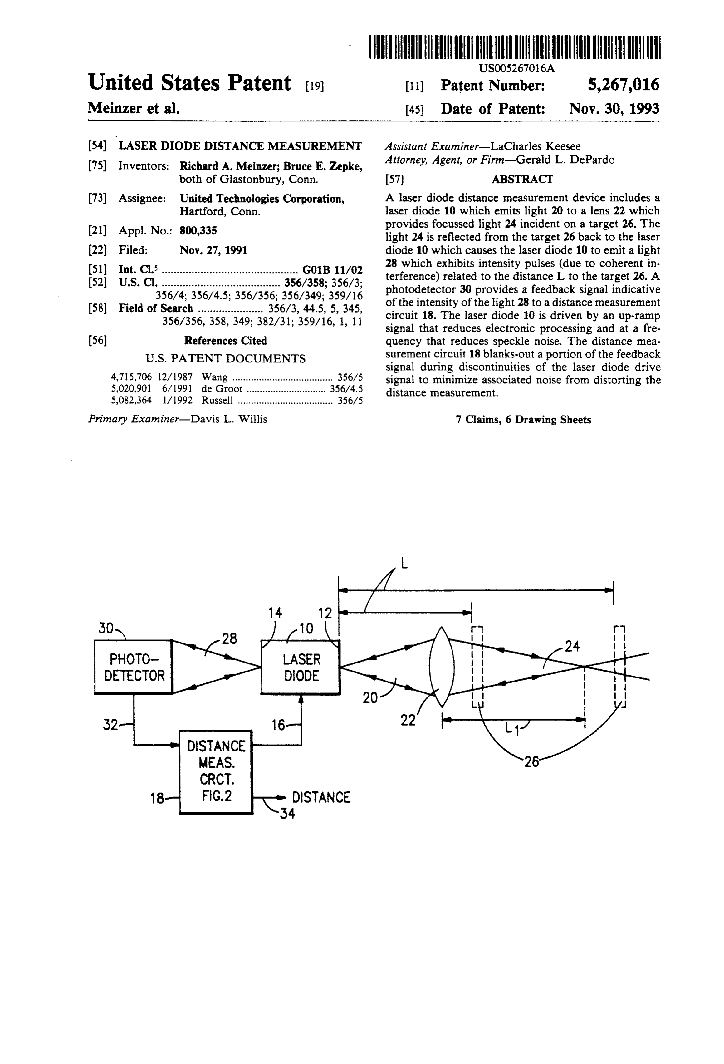
United States Patent (19) 11 Patent Number: 5,267,016 Meinzer et al. (45) Date of Patent: Nov. 30, 1993 54 LASER DIODE DISTANCE MEASUREMENT Assistant Examiner-LaCharles Keesee 75) Inventors: Richard A. Meinzer; Bruce E. Zepke, Attorney, Agent, or Firm-Gerald L. DePardo both of Glastonbury, Conn. (57) ABSTRACT 73) Assignee: United Technologies Corporation, A laser diode distance measurement device includes a Hartford, Conn. laser diode 10 which emits light 20 to a lens 22 which (21) Appl. No.: 800,335 provides focussed light 24 incident on a target 26. The light 24 is reflected from the target 26 back to the laser 22 Filed: Nov. 27, 1991 diode 10 which causes the laser diode 10 to emit a light 511 Int. Cl............................................... GOB 11/02 28 which exhibits intensity pulses (due to coherent in 52 U.S.C. ........................................ 356/358; 356/3; terference) related to the distance L to the target 26. A 356/4; 356/4.5; 356/356; 356/349; 359/16 photodetector 30 provides a feedback signal indicative 58 Field of Search ...................... 356/3, 44.5, 5,345, of the intensity of the light 28 to a distance measurement 356/356, 358, 349; 382/31; 359/16, 1, 11 circuit 18. The laser diode 10 is driven by an up-ramp signal that reduces electronic processing and at a fre (56) References Cited quency that reduces speckle noise. The distance mea
signal during discontinuities of the laser diode drive 4,715,706 12/1987 Wang ...................................... 356/5 signal to minimize associated noise from distorting the 5,020,901 6/1991 de Groot ... ... 356/4.5 distance measurement.
5,082,364 l/1992 Russell .................................... 356/5
Primary Examiner-Davis L. Willis 7 Claims, 6 Drawing Sheets
PHOTO
DETECTOR
DISTANCE
MEAS.
CRCT.
Page 2
Drawing sheet — no readable text.
Page 3
Drawing sheet — no readable text.
Page 4
Drawing sheet — no readable text.
Page 5
Drawing sheet — no readable text.
Page 6
Drawing sheet — no readable text.
Page 7
Drawing sheet — no readable text.
Page 8
Ld (also called effective diode cavity length) which is
LASER DODE DISTANCE MEASUREMENT the product of the index of refraction of the laser mate rial and the physical length of the laser cavity.
CROSS-REFERENCES TO RELATED It is also known that as the optical operating fre APPLICATIONS quency of the laser changes, the intensity of output light Copending U.S. patent application Ser. No. 800,336 emitted from the facet not facing the target will exhibit filed contemporaneously herewith contains subject mat ripples or undulation pulses (also called "mode-hops"). ter related to that disclosed herein. These intensity pulses are due to coherent interference within the laser diode between the light reflected from
TECHNICAL FIELD O the target (that reenters from the facet facing the target) This invention relates to distance measurement and and the light inside the laser diode (provided the dis more particularly to laser diode coherent interference tance from the laser to the target stays fixed). Pulses based distance measurement. occur, as is known, at laser operating frequency inter
BACKGROUND ART
vals equal to the frequency difference between consecu 15 tive external cavity modes:
It is known that semiconductor lasers, such as laser diodes, may be used for measuring distances as de c/2L Eq. 1 scribed by: G. Beheim et al, "Range Finding Using
Frequency-Modulated Laser Diode', Applied Optics, where c is the speed of light and L is the distance from Volume 25, No. 9 (1986). 20 the front facet to the target. It is also known that these A laser diode typically has an optical cavity compris pulses can be readily detected by differentiating the ing two opposing polished ends (called facets) each light intensity signal emitted from the rear facet. having a known index of refraction and having a light If the target is an integral number of laser diode cav amplifying medium therebetween. Light is generated ity optical path lengths Ld from the laser diode, maxi inside the diode cavity by passing electric current 25 mum constructive coherent interference occurs, and the through the p-n junction of the diode (typically using peak amplitude of the output intensity pulses are a maxi ends of the diode other than the facets). The light inside mum. Similarly, if the distance from the target to the the diode cavity is reflected from a first (e.g., front) laser diode is a non-integer multiple of Ld, the peak facet to a second (e.g., rear) facet in a repetitive manner, amplitude of the pulses are reduced due to destructive thereby providing stimulated emission and the well 30 interference of the reflected light, but are still measur known laser action. Typically, the front and rear facets able. Thus, the peak amplitude of the intensity pulses are partially transparent (i.e., not 100% reflective). varies with the distance but are still measurable inde Thus, some light exits the laser from both the front and pendent of whether or not the target is an integer multi rear facets. The amount of light exiting an uncoated ple of Ld from the laser, as described in Lang et al. facet is determined by its index of refraction. 35 In known laser diode distance measurement experi The behavior of a laser diode, as is known, can be ments, such as that described in Lang et al and Beheim significantly affected by external optical feedback, i.e., et al, a known photo detector and accompanying elec feedback of a portion of the laser output light back into tronics have been used to measure the light emitted the laser cavity from an external reflecting surface, as from the rear facet of the laser and to produce a voltage described in the article: R. Lang et al, "External Optical signal indicative thereof. The voltage signal from the Feedback Effects on Semiconductor Injection Laser detector is analyzed to determine distance information. Properties", IEEE Journal of Quantum Electronics, Vol The distance L from the front facet to the target is ume QE-16, No. 3 (March 1980). A laser diode together given by the known equation:
with an external reflective surface, e.g., a reflective target, can be viewed as a compound or coupled laser 45 L=Nc/2AF Eq. 2 cavity consisting of the diode cavity and an external cavity formed by the reflective target and the laser where N is the number of intensity pulses (or external diode facet facing the target (e.g., the front facet). The cavity "mode-hops') that occur over the laser fre distance from the laser to the external surface must be quency change AF; c is the speed of light; and AF is the no longer than one-half the coherence length (the dis 50 change in laser frequency that occurs due to the change tance over which the photons remain in-phase) of the in laser diode drive current. L is very much (many output light because the light must remain coherent orders of magnitude) larger than the optical path length over the entire distance traveled (i.e., out to the target of the laser diode cavity. Thus, the distance L to the and back to the laser). Coupled-cavity effects in con target may be determined by merely counting the num ventional lasers are well known, as described in U.S. 55 ber N of "mode-hops' that result from the laser fre Pat. No. 4,550,410 entitled "Coupled Cavity Laser" to quency change AF. The theoretical resolution in dis Chenausky et al. tance measurement, as is known, is the distance corre It is also known that if the current through a laser sponding to one "mode-hop" or:
diode is changed from one level to another, the optical frequency that the laser diode operates at (or "lases' at; AL= c/2AF Eq. 3 also called the "free running' frequency) will change in response thereto. More specifically, when the current is Thus, if AF =50 GHz, then AL=3 mm, which is good increased, the wavelength of the laser diode gets longer resolution, as discussed in Beheim et al. and, thus, the frequency that it operates at decreases. However, numerous problems occur in attempting to This occurs, as is known, because the temperature of the 65 implement laser diode coherent interference-based dis laser diode material changes with current, which causes tance measurement in a real-world environment. First, a change in the index of refraction of the material, one of the largest problems with coherent light detec which causes a change in the cavity optical path length tion is speckle noise. Speckle noise, as is known, is an
Page 9
optical noise generated as a consequence of the scatter ond output light having an intensity related to the dis ing of coherent light when it hits a surface that is not tance from the laser to the target; the second output perfectly flat (on a wavelength scale). Also, all targets light is converted to a signal solely proportional to the exhibit a finite amount of surface vibration, which in distance to the target; the laser operating frequency is creases speckle noise. Furthermore, if the target is rotat modulated at a rate which minimizes optical speckle ing, such as a helicopter rotor blade (like that described noise.
in copending U.S. patent application Ser. No. According further to the invention, the laser drive 07/665,061, filed Mar. 6, 1991), some wobble will exist signal has a shape chosen so as to minimize electronics. which also increases speckle noise. This noise interferes According still further to the invention, a portion of the with coherent detection and can cause the optical inten 10 optical feedback signal is not used (blanked-out) to sity to drop-off periodically as a function of distance to prevent disruption of the distance measurement due to the target, thereby preventing intensity measurement at abrupt changes in the current waveform (i.e., when certain distances (i.e., measurement drop-out) and mak intensity discontinuities occur) and/or due to electronic ing distance measurement unreliable. noise (caused by signal differentiation or other signal Second, Beheim et al discusses using an up-down 15 processing).
ramp (positive sloped ramp followed by a negative The present invention employs techniques which sloped ramp) current waveform to drive the laser diode; improve accuracy and realizability of laser distance however, an up-down ramp produces a DC shift in the measuring sensors by reducing speckle, minimizing differentiated waveform which varies as a function of electronics, and minimizing the effects of current drive the number of pulses seen over a given ramp time, 20 discontinuities which can cause inaccuracies in distance thereby causing nonuniform pulse amplitudes, which measurement. The invention may be used for any dis can lead to inaccurate distance measurement. Further tance measurement application, e.g., a back-up obstruc more, an up-down ramp can generate intensity pulses in tion detector for an automobile, to position an elevator two opposite polarities, requiring electronics that de car in a hoistway to close-in to a floor position, or to tects both polarities. Also, the up-down ramp waveform 25 determine vehicle ride-height. A further advantage of introduces inaccuracy due to the abrupt change in the the invention is that it uses coherent light; thus, it re waveform slope (from positive to negative). quires minimal optical backscatter (nanowatts) and it is Also, it is known that if the target is in motion (i.e., undisturbed by incoherent light such as sunlight, street has a finite velocity), additional pulses (with similar lights, or car headlights.
amplitude characteristics as those discussed hereinbe 30 The foregoing and other objects, features, and advan fore) will appear on the laser output signal due to a tages of the present invention will become more appar known Doppler effect (called the Doppler frequency ent in the light of the following detailed description of Fd). This occurs whether or not the laser diode drive exemplary embodiments thereof, as illustrated in the current (i.e., the laser optical frequency) is changing accompanying drawings.
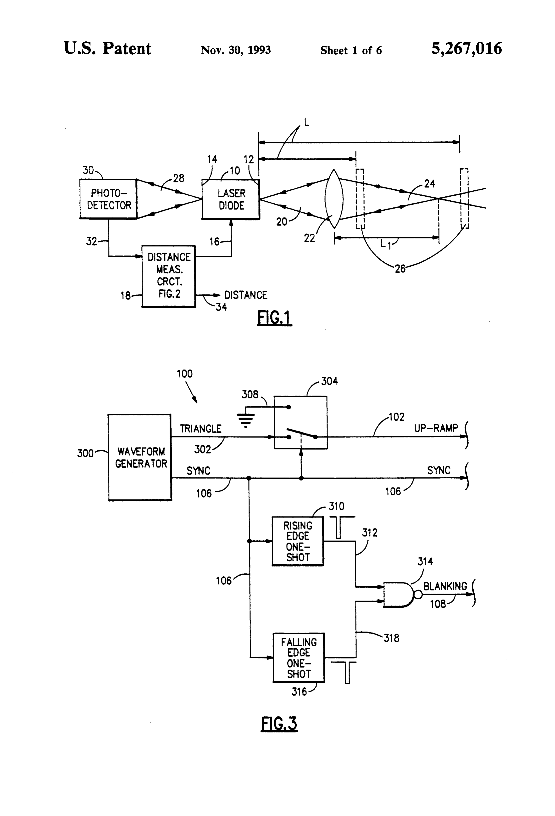
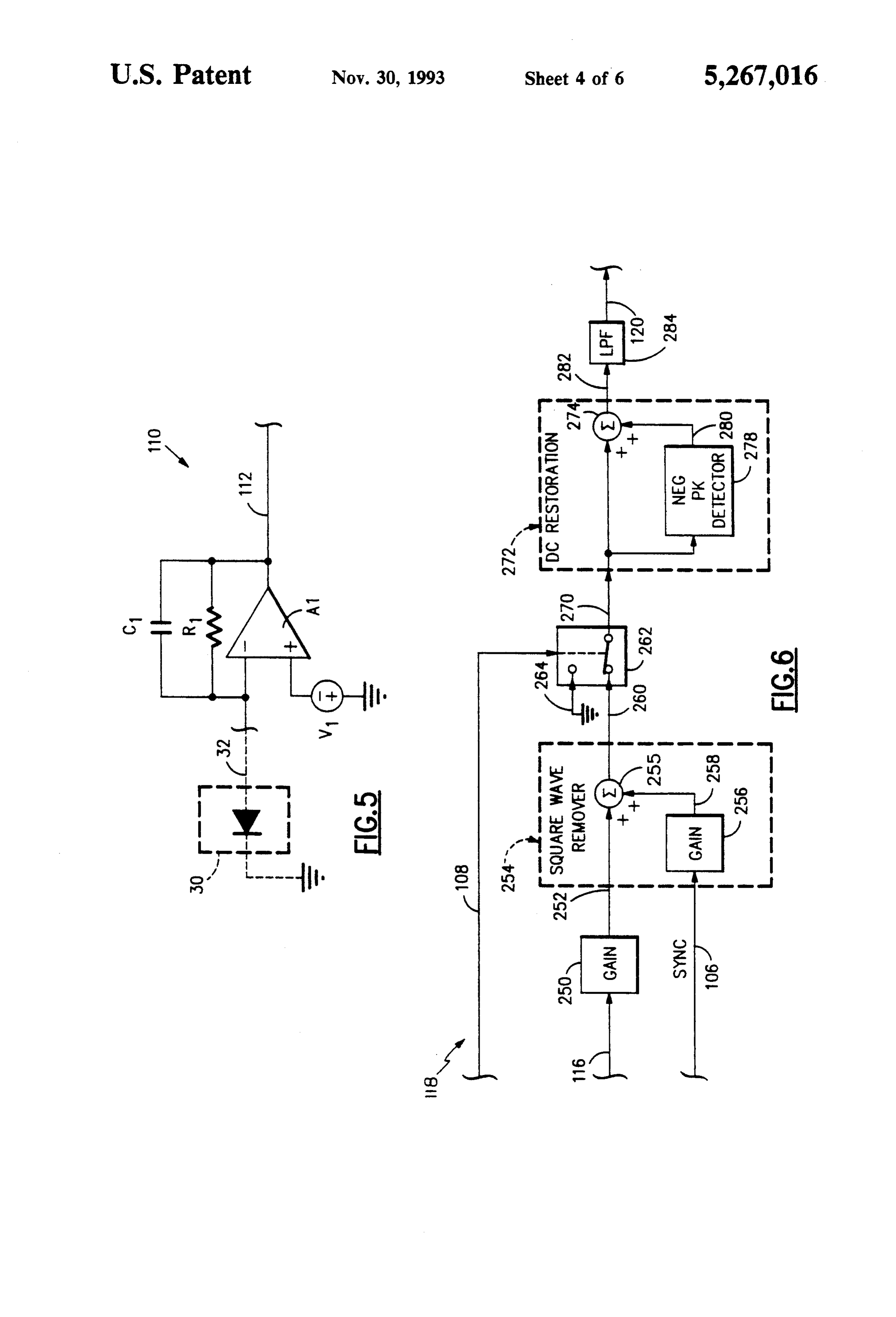
with time. Consequently, the total number of pulses per 35 BRIEF DESCRIPTION OF THE DRAWINGS sweep of the drive current (herein called a ramp cycle) emitted from the laser is related to the distance (Fx) and FIG. 1 is a schematic block diagram of a distance the velocity (Fd) of the target. More specifically, for an measuring device in accordance with the present inven up-down current ramp drive signal, when the drive tion.
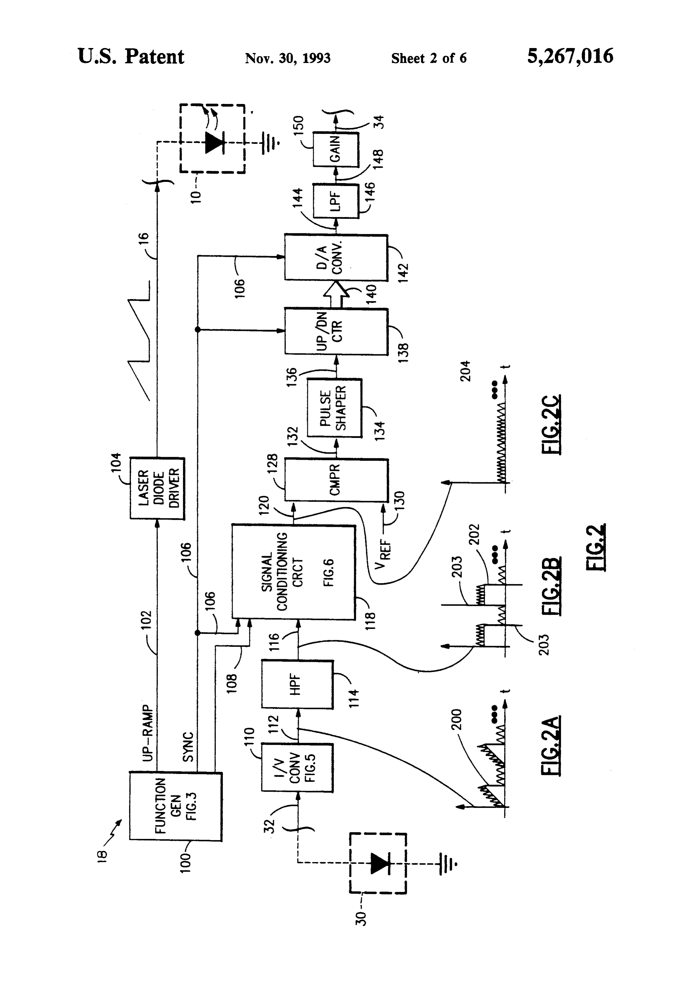
current is increasing and the target is moving toward FIG. 2 is a schematic block diagram of a distance the laser, the number of pulses seen on the feedback is: measuring circuit within the distance measuring device Fx--Fd. Conversely, when the drive current is decreas of FIG. 1 including illustrations: (a) a plot of pulses ing and the target is moving toward the laser, the num superimposed on a drive waveform, (b) a plot of an ber of pulses seen is: Fx-Fd. If Fd is greater than Fx exemplary signal from a high pass filter, and (c) a plot of (i.e., the target is moving faster than a certain speed) the 45 an exemplary signal from a signal conditioning circuit. result of the relation: Fx-Fd, is negative and the direc FIG. 3 is a schematic block diagram of a function tion of the pulses on the decreasing slope will change generator circuit within the distance measuring circuit polarity, thereby requiring the electronics to compen of FIG. 2.
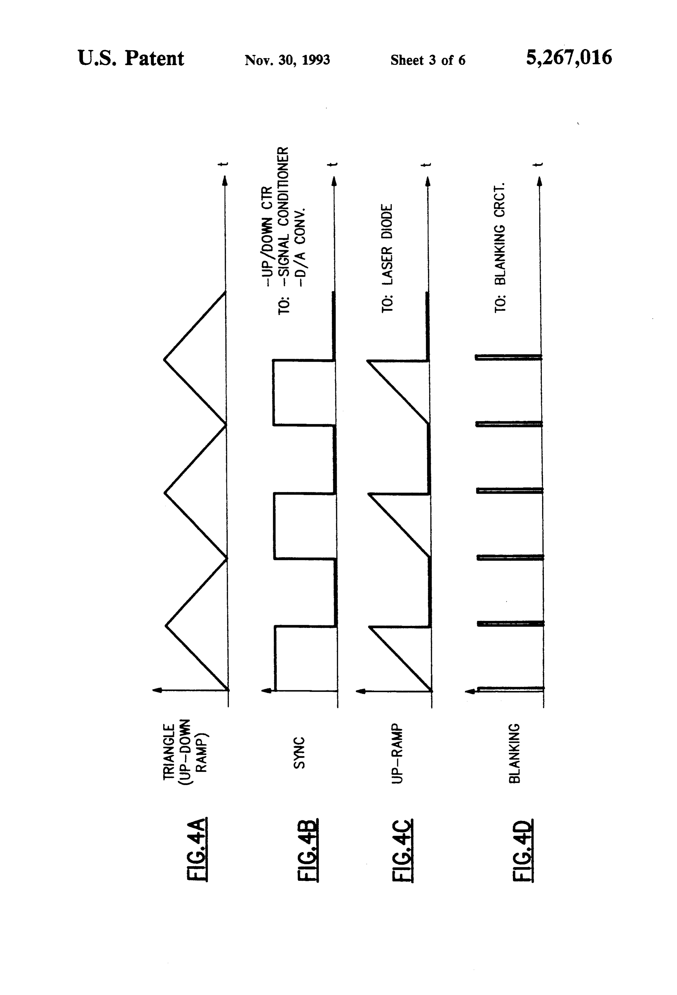
sate for this occurrence. This requires the electronics to FIG. 4(a-d) are plots of signals generated by the be much more complex and costly, or that velocity 50 function generator circuit of FIG. 3.
constraints be placed on the target. If the target is mov FIG. 5 is a schematic block diagram of a current-to ing away from the laser, the above relationships are the voltage (I/V) converter within the distance measuring same except the sign of Fd is reversed for both cases. circuit of FIG. 2.
DISCLOSURE OF THE INVENTION FIG. 6 is a schematic block diagram of a signal condi 55 tioning circuit within the distance measuring circuit of
Objects of the invention include provision of laser FIG. 2.
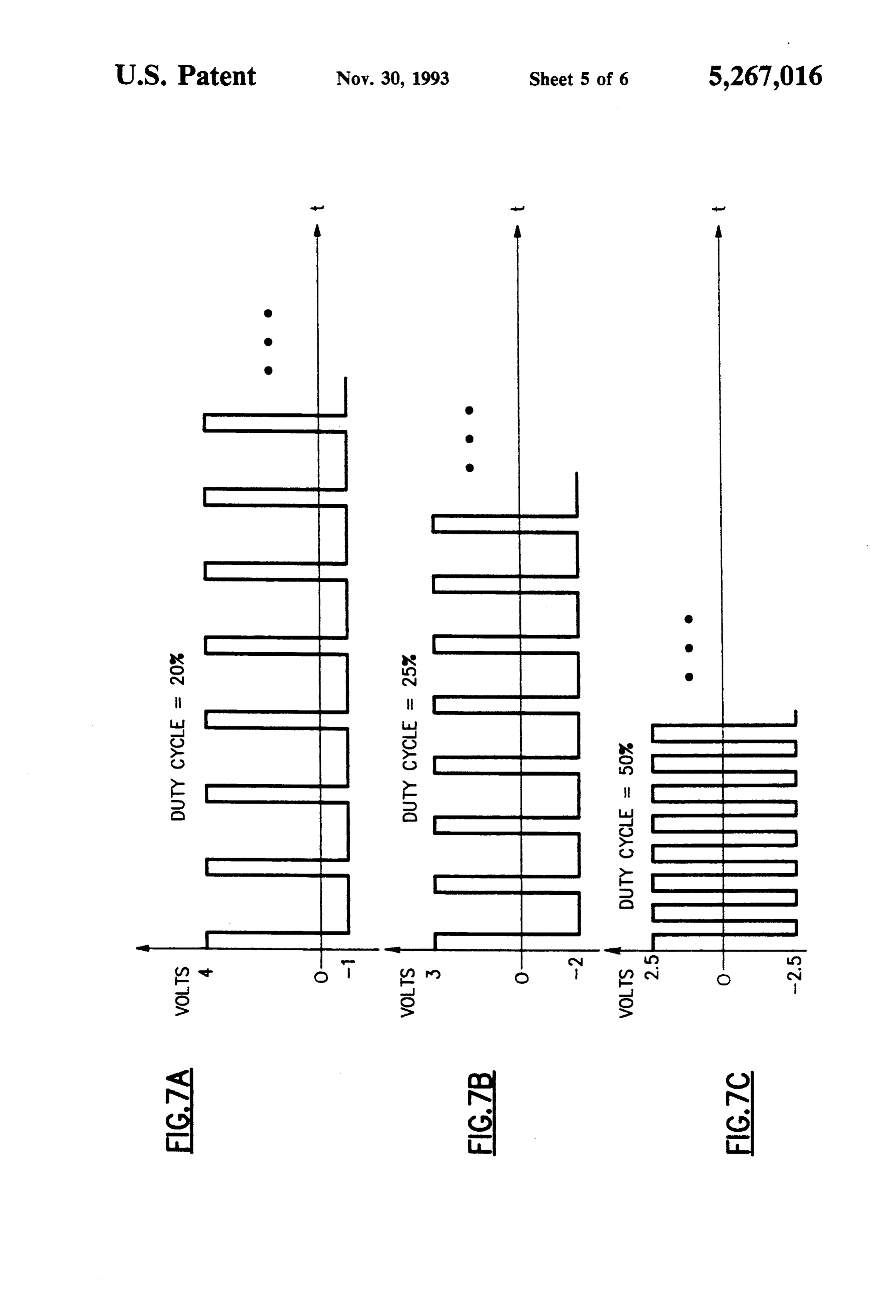
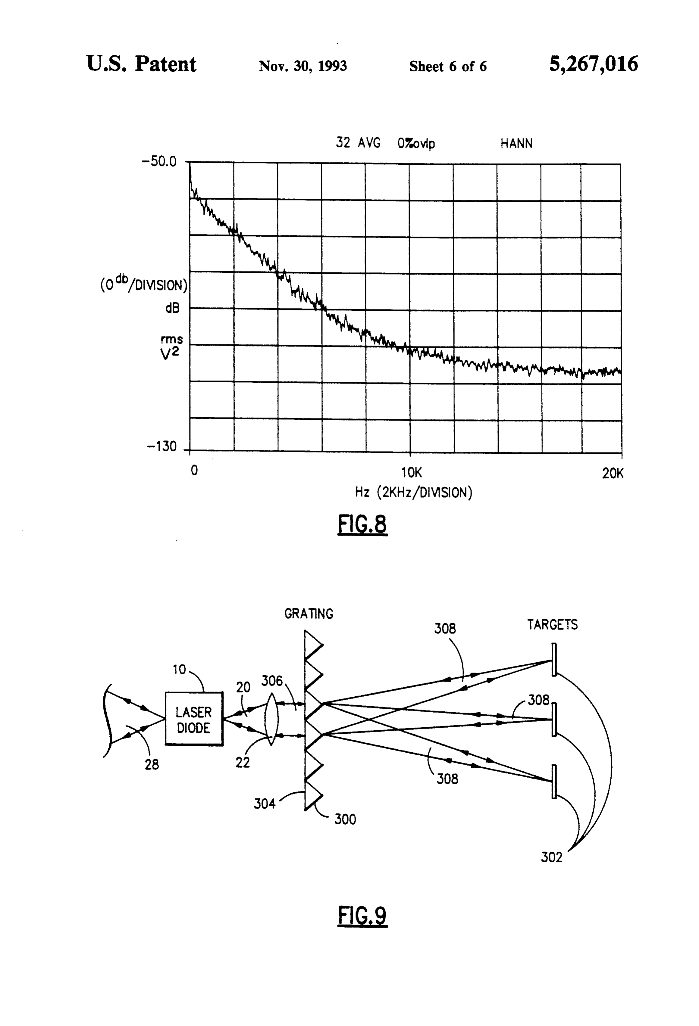
based distance measurement, which reduces speckle FIG. 7 (a-c) are plots of exemplary signals from a noise, which uses minimal electronics, which minimizes high pass filter of FIG. 2 having various duty cycles. inaccuracies caused by discontinuities of the laser drive FIG. 8 is a plot of the speckle noise against frequency, signal, and which does not put velocity constraints on showing that speckle noise decreases with increasing the target. frequency.
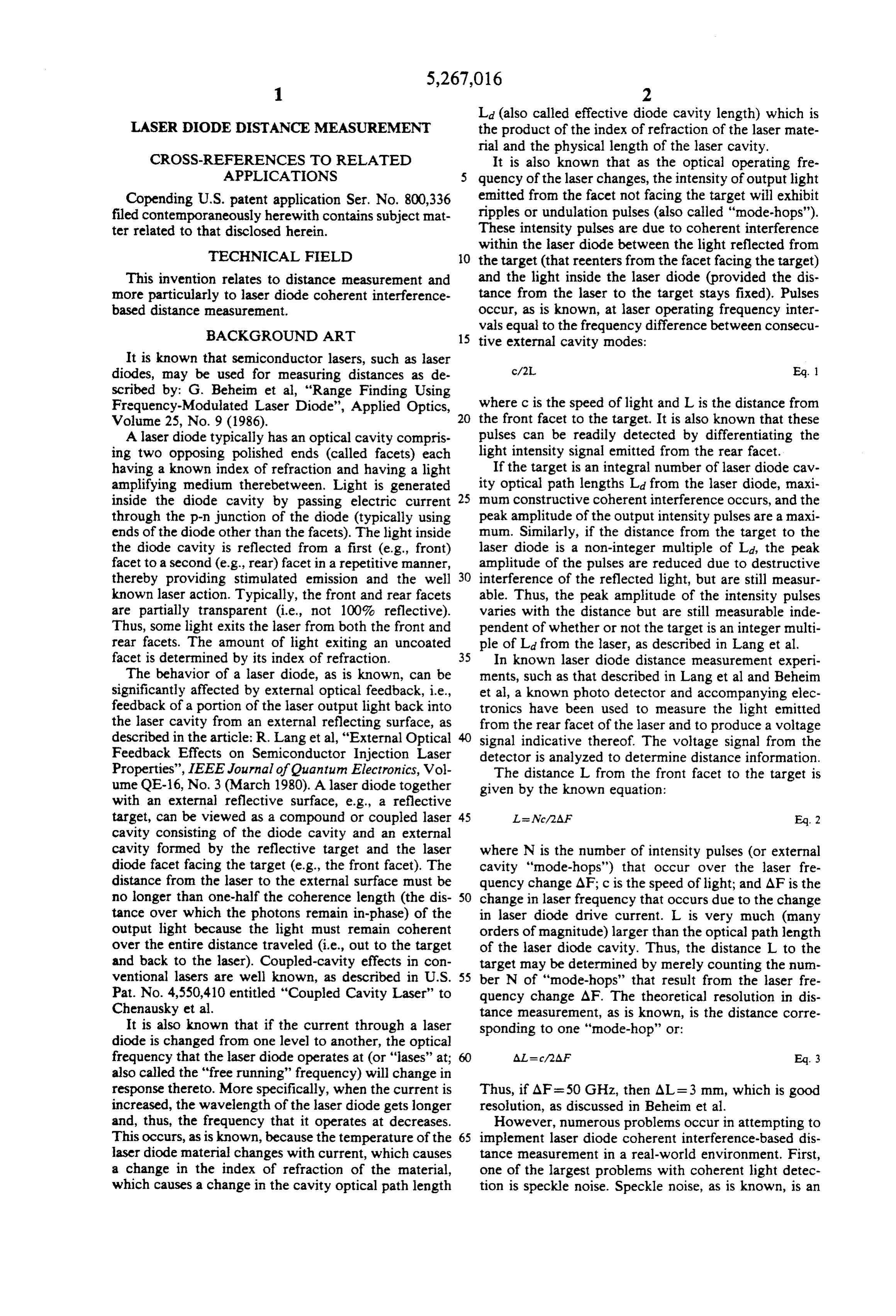
According to the present invention, a laser, such as a FIG. 9 is a diagram showing a configuration of the laser diode, having a variable operating frequency con present invention using a plurality of targets. trolled by a laser drive signal, emits a first output light BEST MODE FOR CARRYING OUT THE which is incident upon a target; the first output light is 65 INVENTION scattered by the target and fed back into the laser; co herent interference occurs between the scattered light Referring to FIG. 1, a laser diode distance measuring and the light within the laser, thereby producing a sec device includes a known laser diode 10, e.g., a Mit
Page 10
subishi ML3101 laser diode with built-in photodiode, ramps from 0 to 20 millivolts, on the line 102 to a cur having a front facet 12 (or polished end) which is ap rent ramp signal that ramps from 29 to 31 milliamps proximately 10% reflective and a rear facet 14 which is (FIG. 4, Illust. c) on the line 16 which drives the laser approximately 40% reflective. More light exits from the diode 10. Other laser diode drivers and other voltage side with the lower reflectivity, as is known. The laser and current ramp ranges may be used if desired. The diode 10 is made of a semiconductor material, e.g., invention drives the laser diode 10 in the active region aluminum gallium arsenide (AlGaAs), and basically of the diode with a current drive (up-ramp) waveform comprises a PN junction, i.e., P-doped AlGaAs mono signal on the line 16 comprising a positive slope ramp lithically adjacent to N-doped AlGaAs having various followed by a zero slope down-step (FIG. 4, Illust. c), concentrations of the constituent materials. Polishing 10 with a dc offset of approximately 30 milliamps. Other the ends of the semiconductor promotes a phenomenon signal offsets and ranges may be used if desired. The known as Fresnel reflection which determines reflectiv sweep frequency of the current drive waveform on the ity based on the refractive index of the material. Other line 16 is 1KHz; however, other frequencies may be characteristics of the laser diode are as follows: wave used if desired, as discussed hereinafter. The function length=830 nanometers; coherence length=approxi 15 generator 100 also provides a sync signal on a line 106 mately 4 meters; and output powers approximately 3 and a blanking signal on a line 108 (both discussed here milliwatts. Other semiconductor lasers may be used if inafter).
desired provided half the coherence length is less than Referring now to FIG. 3, the function generator 100 the desired distance to the target (as discussed hereinbe includes a triangular (up-down ramp) waveform gener fore) and the power level is adequate relative to the 20 ator 300, e.g., an Intersil 8038. The triangular waveform distance to the target. The laser diode 1 is driven by an generator provides a triangular waveform signal (FIG. electric current signal on a line 16 from a distance mea 4, Illust, a) on a line 302 to one input of a switch 304, surement circuit 18 (discussed hereinafter). e.g., Analog Devices, Analog Switch, Part No. The front facet 12 of the laser diode 10 emits diver AD7512. The other input of the switch 304 is connected gent light 20 to a known lens 22, e.g., a graded index rod 25 to a line 308 which is connected to ground (Ov). The microlens (GRIN lens), Nippon Sheet Glass Company triangular waveform generator 300 also provides a (NSG), Part No.W30-01 10-078, having a diameter of 3 square wave signal (or sync signal; FIG. 4, Illust b) on mm, a length of 3.3 mm, and an anti-reflective coating. the line 106 which is fed to, among other things, the Typically, the lens 22 is disposed on the front facet 12 of switch 304. The sync signal is high (e.g., --5v) during the laser diode 10 with no space therebetween; how 30 the positive slope of the triangular waveform, and is ever, there may be space between them if desired. The low (e.g., Ov) during the negative slope of the triangular lens 22 converts the divergent light 20 into a focused waveform (FIG. 4, Illust, a). When the sync signal on beam 24. The beam 24 is focused on a fixed distance L1, the line 106 is high, the switch 304 connects the triangu e.g., two feet, from the lens 22. A target 26 has a vari lar waveform signal on the line 302 to the line 102. able unknown distance L, ranging from 6" to 3'6", from 35 When the sync signal on the line 106 is low, the switch the front facet 12, which is calculated by the invention. 304 connects the Ov signal to the line 102. The resultant Other ranges for the distance L to the target 26 may be voltage signal (FIG. 4, Illust. c) on the line 102 provides used if desired provided the laser intensity is high the desired laser diode current drive waveform, with a enough to provide adequate optical feedback. Alterna dc offset, on the line 16 (FIGS. 1, 2). tively, a collimated beam may be used instead of the The sync signal on the line 106 is also connected to focussed beam 24, provided the diameter is small the rising-edge input of a first one-shot device 310, e.g., enough, e.g., 1/16", and/or the intensity is high enough National Semiconductor, Part No. CD4528B, which to provide adequate optical feedback. Coherent light provides a low pulse of a predetermined time duration, from the lens 22 is reflected from the target 26 back e.g., 10 microseconds, on a line 312 when the sync sig through the lens 22 into the laser diode 10 through the 45 nal changes from a low to a high state. The line 312 is front facet 12, where constructive interference occurs connected to one input of a NAND gate 314. Similarly, within the laser diode 10, as discussed hereinbefore. The the line 106 is connected to the falling-edge input of a target 26 may be made of any material, e.g., plastic, second one-shot device 316 having a low pulse output wood, or metal, provided it scatters coherent light of signal on a line 318 when the sync signal changes from the wavelength produced by the laser diode 10. 50 a high to a low voltage. The line 318 is connected to the The rear facet 14 of the laser diode 10 emits divergent other input of the NAND gate 314. The NAND gate light 28 which is incident upon a photodetector 30 (or 314 provides an output signal on the line 108, that is photodiode). The output light 28 from the rear facet 14 high when either input signal to the NAND gate 314 is exhibits intensity pulses related to the distance L to the low. Thus, the signal on the line 108 exhibits a high target 26, as discussed hereinbefore. The laser diode 10 55 pulse when either one-shot, 310 or 316, produces a low and the photodiode 30 are typically one complete as pulse; otherwise, the signal is high. The resulting wave sembly; however, separate parts may be used if desired. form (FIG. 4, Illust. d) is a narrow high pulse at the The photodetector 30 provides an electric current sig beginning and end of each period of the up-ramp wave nal on a line 32, indicative of the intensity of the light 28 form (FIG. 4, Illust. c) and is called a blanking signal incident thereon, to the distance measurement circuit (discussed hereinafter).
18. The distance measurement circuit 18 converts the Referring to FIG. 2, the current from the photodiode current signal on the line 32 to a voltage signal on a line 30 on the line 32 is provided to a known current-to-volt 34 indicative of the distance L to the target 26. age (I/V) converter 110 which converts the input cur Referring to FIG. 2, the distance measurement circuit rent to an output voltage on the line 112, having charac 18 includes a function generator 100 which provides a 65 teristics similar to the input current, i.e., ramps and voltage signal on a line 102 to a laser diode driver 104, pulses related to intensity changes, but with units of e.g., a Melles Griot, Part No. 06DLD201. The laser voltage. As shown in FIG. 5, the I/V converter 110 diode driver 104 converts the voltage ramp signal that comprises a high-bandwidth low-noise operational am
Page 11
plifier Al (opamp), e.g., OP470, the photodiode 30, a the resulting signal is provided on a line 260 having the resistor R1 (e.g., 2 k ohms), a capacitor C1 (e.g., 50 square wave component removed. picofarads), and a bias voltage V1 (e.g., -3 volts). The We have found that when the diode current drive output voltage on the line 112 is related to the current signal on the line 16 abruptly changes slope (i.e., exhib through the photodiode 30, the value of the resistor R1, its a discontinuity), high frequency harmonics are gen and the value of the bias voltage V1. The feedback erated on the optical feedback signal causing additional capacitor C1, together with the parallel resistor R1, pulses to occur for a short time, e.g., 10 microseconds, serves to reduce high frequency noise by attenuating near the discontinuity, thereby distorting the distance frequencies greater than 1.6 MHz. The bias voltage V1 measurement. We have also found that the signal on the shifts the dc level of the output voltage to the desired O line 116 exhibits spikes 203 (FIG. 2, Illust. b) on the level. The change in output ramp voltage is about 150 rising and falling edges of the signal due to the differen millivolts, corresponding to a change in the laser diode tiator effects of the HPF 114 and causes an overall shift 10 drive current ramp (and hence output intensity) of 29 in the signal level which causes inaccuracies in the mea to 31 mA. Similarly, voltage pulses ranging from 1 to 2 surement of the pulses. Furthermore, we have found millivolts peak correspond to current pulses indicative 15 that zeroing or blanking-out the signal during this time of the optical coherent interference discussed hereinbe eliminates this measurement distortion without sacrific fore. Other electronic configurations for the I/V con ing any appreciable accuracy. The signal on the line 260 verter 110 may be used if desired. The signal on the line from the square wave remover circuit 254 is fed to one 112 is similar to a waveform 200 (FIG. 2, Illust, a). The input of a switch 262, e.g., Analog Devices, Analog voltage signal on the line 112 is provided to a high pass 20 Switch, Part No. AD7512. The other input of the filter 114 which acts as a differentiator to separate and switch 262 is connected to a line 264 which is connected amplify the high frequency pulses (FIG. 2, Illust, a) to ground (Ov). The blanking signal (FIG. 4, Illust. d) on from the low frequency up-ramp (FIG. 4, Illust, c). the line 108 from the function generator 100 is also fed More specifically, the high pass filter 114 is a single pole to the switch 262 and controls the selection of the out filter with a positive slope of 20db/decade having a DC 25 put signal provided on a line 270. When the blanking gain of zero and a break frequency of 120 KHz beyond signal is high, the switch 262 connects the signal from which the magnitude of the filter gain is flat at again of the square wave remover circuit 254 on the line 260 to 10. The output of the high pass filter 114 provides a the line 270, Similarly, when the blanking signal is low, differentiated signal similar to that shown by the wave the switch 262 connects the 0 V signal on the line 260 to form 202 (FIG. 2, Illust. b). The filter 114 is made from 30 the line 270. As discussed hereinbefore, the blanking opamps, e.g., OP470, resistors, and capacitors in a signal (FIG. 4, Illust. d) exhibits a short duration pulse known negative feedback configuration, e.g., a 500 during discontinuities of the current drive up-ramp picofarad capacitor in series with a 2.7 kohm resistor signal (FIG. 4, Illust, c), i.e., at the beginning and the connected to the negative input; a 27 kohm negative end of the ramp portion. Thus, the output signal on the feedback resistor; and a direct connection from the 35 line 270 looks just like the input signal on the line 260 positive input of the opamp to ground. Other opamps except that the signal is set to Ov for a short period, e.g., and component configurations may be used if desired. 10 microseconds, at the beginning and end of the cur The differentiated signal from the high pass filter 114 rent ramp (due to the blanking signal pulses). Thus, is provided on a line 116 to a signal conditioning circuit these pulses, in effect, blank-out the signal on the line 118. The signal conditioning circuit 118 amplifies the 260. It may not be required to provide a pulse at the signal on the line 116, e.g., by 50, removes the square beginning of the ramp if this portion of the ramp signal wave component from the waveform, zeros (or blanks increases at a very gentle rate so as not to introduce any out) a portion of the signal, shifts the dc level of the high frequency components in the optical feedback signal to provide a consistent value (Ov) for the low signal scattered back from the target 26 and not to cause portion of the signal, and provides some limited high 45 the high pass filter to generate a spike. frequency filtering. The resulting signal (FIG. 2, Illust. The signal conditioning circuit 118 also includes a c), provided on a line 120, has a series of pulses extend DC restoration circuit, to which the signal on the line ing from a common minimum voltage (reference plane) 270 is fed, which shifts the input signal such that the low of approximately zero volts. Other common minimum magnitude portion of the signal is always the same value voltages may be used if desired. 50 e.g., Ov. The signal on the line 270 is fed to a first input More specifically, referring to FIG. 6, the signal of a summer 274 and also to a negative peak detector conditioning circuit 118 includes again stage 250, com 278. The negative peak detector 278 provides a positive prising known electronics such as opamps and resistors, signal on the line 280 indicative of the average lowest which amplifies the differentiated signal on the line 116 value (e.g., within the past 2 milliseconds) of the input by 50. Other gain stages may be used if desired. The 55 signal. The signal on the line 280 is fed to a second input amplified differentiated signal is provided on a line 252 of the summer 274, thereby shifting up the signal on the to a square wave remover circuit 254 which removes line 270 by the amount it was below zero volts. The the square wave component of the differentiated ampli resultant signal is provided on a line 282. fied signal on the line 252 (compare Illusts. b and c, Referring to FIG. 7, to illustrate the need for the dc FIG. 2). The signal on the line 252 is fed to a first input restoration circuit 272, when the duty cycle (i.e., the of a summer 255. The sync signal (FIG. 4, Illust. b) on percentage of time the pulse is high compared to the the line 106 is fed to a gain stage 256 which shifts the total period) of the waveform changes, the dc level of magnitude of the sync signal to the same magnitude and the signal changes. However, because the high pass opposite sign of the square wave component of the filter 114 has a 0 dc value output signal, the average amplified differentiated signal on the line 252. The out 65 value of the output signal will always be zero, indepen put signal from the gain stage 256 is provided on a line dent of the duty cycle. This means that a pulse having 258 to a second input of the summer 255. The summer the same amplitude will appear to have a different am 255 adds the signals on the two input lines 252,258 and plitude when compared to the same reference, e.g., Ov
Page 12
as shown in FIG. 7, thereby causing incorrect counting will count down one count for each pulse which ap of pulses. The signal on the line 282 will be similar to the pears along that portion of the waveform. Thus, the waveforms shown in FIG. 7 except that the lowest resultant number of counts in the counter after one portion of the wave form will be shifted up to Ov. Other sweep period of the up-ramp waveform is the difference polarities of the signals may be used if desired. between the number of pulses on the positive slope The signal from the dc restoration circuit 272 on the portion of the input signal (FIG. 2, Illust. a; indicative of line 282 is fed to a known low pass filter 284 comprising the distance to and velocity of the target 26) on the line opamps, resistors, and capacitors, configured in a 112 and the number of pulses on the flat portion of the known negative feedback arrangement. The break fre same signal (indicative of the velocity of the target 26). quency of the filter 284 is 1 MHz. The filter removes 10 Thus, the counter provides a digital binary signal N unwanted high frequency noise from the signal before proportional to the distance L to the target 26 as dis being fed to the rest of the circuit on the line 120. An cussed hereinbefore (i.e., L = Nc/2AF). Other size other or no low pass filter may be used if desired, de counters may be used if desired; however, the maximum pending on the amount and frequency of the noise pres number of pulses occurring and the time period for each ent. Other circuit configurations for the signal condi 15 sweep of the waveform must be considered in choosing tioning circuit 118 or any part thereof may be used if the size of the counter.
desired. The value of the digital binary signal in the counter is The signal on the line 120 from the signal condition provided on a plurality of lines 140, one for each bit, ing circuit 118 is fed to a first input of a comparator e.g., 12 lines, to a D/A converter circuit 142 comprising circuit 128. A reference voltage signal Vref is provided 20 an input buffer, e.g., 74LS174, and a D/A converter, on a line 130 to a second input of the comparator circuit e.g., Analog Devices, Part No. DAC80P. The D/A 128. The magnitude of the reference signal is set to a converter circuit 142 converts a binary digital signal on predetermined level, e.g., using a voltage divider, above the lines 140 from the up-down counter 138 to an analog the noise floor of the differentiated, pulsed, blanked-out, signal indicative thereof on a line 144. The D/A con signal on the line 126, and below the lowest peak of the 25 verter circuit 142 performs a conversion each time it pulses expected on the input signal. The comparator receives a rising edge of the sync signal (FIG. 4, Illust. provides an output signal on a line 132 having either a b) on the line 106 from the ramp generator 100. When low, e.g. Ov, or a high, e.g., 5v, state. When the magni the rising edge of the sync signal occurs, the digital tude of the input signal on the line 126 is greater than binary signal on the lines 140 are latched by the buffer the magnitude of the reference voltage on the line 130, 30 in the D/A converter circuit 142, thereby preventing the output signal of the comparator circuit 128 on the subsequent changes in the up-down counter 138 from line 132 is high. Conversely, when the magnitude of the affecting the D/A conversion until the next rising edge input signal is less than the magnitude of the reference of the sync signal.
signal, the output signal of the comparator circuit 128 The analog output signal from the D/A converter on the line 132 is low. The comparator circuit 128 com 35 circuit 142 is provided on a line 144 to a known low pass prises a known comparator, e.g., LM211H, with posi filter 146. The low pass filter 146 comprises an opamp, tive feedback added to provide hysteresis, e.g., +/-5 resistors, and capacitors in a known negative feedback millivolts, to the threshold set by the reference signal, arrangement. The break frequency of low pass filter is 3 thereby avoiding spurious noise from causing the out Hz; however, other frequencies may be used if desired. put signal to change state. The comparator circuit 128 The low pass filter 146 provides a signal on a line 148 also provides pulses having a more uniform output am indicative of the average value of the analog signal on plitude, e.g., 5 volts, and less noise than the input signal the line 144, thereby providing an averaged analog on the line 126. Other configurations for the comparator voltage signal proportional to the distance L to the circuit 128 may be used if desired. target 26.
The signal from the comparator circuit 128 on the 45 The signal on the line 148 is fed to a gain stage 150, line 132 is fed to a known pulse shaper 134 comprising, which multiplies the magnitude of the signal on the line e.g., a Schmitt trigger buffer or a one-shot. The pulse 148 by a predetermined value, e.g., c/2AF, to provide a shaper 134 provides a signal on a line 136 that is cleaner, signal on a line 152 indicative of the distance L to the i.e., the pulses are more square and the edges more target in the desired units, e.g., feet. vertical, than the signal from the comparator 128 on the 50 Referring now to FIG. 8, it is known that with a line 132. constant (dc) current drive signal driving the laser The output signal from the pulse shaper 134 on the diode 10 (i.e., with the laser running at a constant opti line 136 is fed to a known 12 bit up-down digital counter cal frequency), the magnitude of the speckle noise com 138, e.g., three 4-bit 74LS169B counters in series. The ponent (in db/hz) on the optical feedback decreases as up-down counter 140 counts the number of pulses either 55 the frequency increases, i.e., the noise component of the in an up direction (each pulse received increments the feedback signal on the line 32 (FIG. 1) exhibits a fre counter by one count) or a down direction (each pulse quency spectrum which has high amplitude energy at received decrements the counter by one count) as deter low frequencies and low amplitude energy at high fre mined by the sync signal on the line 106 from the ramp quencies. We have found that by increasing the sweep generator 100, i.e., a high signal on the line 106 causes frequency of the current ramp waveform, the speckle the counter 138 to count up and a low signal causes it to noise reduces in amplitude (similar to the frequency count down. During the positive slope of the up-ramp spectrum). Reduced speckle noise reduces the overall waveform (FIG. 4, illust c), the sync signal on the line noise floor of the feedback signal and allows the com 106 is high, and the up-down counter will count up one parator circuit 128 (FIG. 2) to detect the correct nun count for each pulse which appears on the signal on the 65 ber of pulses due to target distance and/or velocity on line 136 from the pulse shaper 134. Similarly, during the the ramp or the flat portion of the feedback waveform. zero slope portion of the up-ramp waveform, the sync Current applications, e.g., using an up-down ramp drive signal on the line 106 is low, and the up-down counter signal, use sweep frequencies of less than 100 Hz. The
Page 13
ramp sweep frequency used herein is 1 kHz which may prior to other signal conditioning such as differentia be increased to 20 khz and higher if desired, to provide tion. Furthermore, instead of counting pulses, the feed more speckle reduction. The higher the ramp fre back signal may be analyzed using a known frequency quency, the lower the speckle noise, and, thus, the more spectrum analyzer and then converting the resultant accurate the distance measurement. The speed of the frequency to the number of pulses on the feedback sig electronics is the only limiting parameter in increasing nal, knowing the time over which the signal was ana the sweep frequency. The speckle noise shown in FIG. lyzed. However, it should be understood that the pulses 8 was obtained using a continuous time spectrum analy may not have equal time spacing between them, thereby Zer averaging 32 samples through a Hanning window. producing a broad frequency spectrum from which the Referring now to FIG. 9, it should be obvious to pulse frequency must be extracted.
those skilled in the art that the invention may be used to 10 Other patents relating to optical coherent distance detect the distance to one of a plurality of targets 300 by measurement include U.S. Pat. No. 4,733,609, Goodwin laterally dispersing the light using a grating 302 having et al.
a nonreflective surface 304. In that case, the lens 22 is Although the invention has been described and illus placed a distance from the laser diode so as to provide 15 trated with respect to exemplary embodiments thereof, a collimated beam 306 to the grating 300 which con it should be understood by those skilled in the art that verts the light into a plurality of laterally dispersed the foregoing focussed beams 308. The target having the closest dis additions mayand various other changes, omissions and tance to the lens 22 will produce the largest intensity spirit and the scopemade
of the without departing from the invention.
magnitude pulses on the optical feedback signal. There We cairn:
fore, a comparator with a variable threshold or a plural 1. A laser-based distance measuring device for mea ity of comparators with different thresholds may be suring the distance to a target, comprising: used to calculate the distance to the closest target (ideal a laser, having a variable optical operating frequency, for use as a collision detector). Alternatively, the grat and having a first facet and a second facet for emit ing 300 may be incorporated into the lens 22 as one ting a first output light from said first facet toward assembly. Instead of a grating 300, one or more prisms, 25 the target and for emitting a second output light or beam splitters, or rotating components may be used from said second facet;
to disperse the light. Also, optical switches, such as the first output light being incident on the target and electronically controlled polarizers, may be placed in having a wavelength which allows it to be scat the path of the individual beams to switch the beams in tered by the target back into said laser; and out.
As discussed hereinbefore, the direction the target is 30 laser drive means, for providing a variable laser drive moving determines the polarity of the pulses of the signal to said laser for varying the optical operating differentiated signal (i.e., whether the pulses extend in frequency of said laser, said laser drive signal hav the positive or negative direction). More specifically, ing a predetermined periodic sweep frequency set when the target is moving toward the laser, the pulses to minimize speckle noise; due to velocity appear in the positive direction, and 35 thethesecond output light having an intensity related to distance from said front facet to the target due when moving away from the laser, the pulses due to to coherent interference within said laser between velocity appear in the negative direction. Therefore, the scattered light from the target and light within even though the invention has been described as being said laser;
used with the target traveling in a single direction, i.e., optical detection means, responsive to the second toward the laser, it should be understood by those output light, for providing a feedback signal indica skilled in the art that the electronics may be easily modi tive of the intensity of the second light; and fied to be used for detecting targets traveling in either direction, i.e., detect both positive and negative going distance measurement means, responsive to said feed pulses. back signal from said optical detection means, for It should be understood by those skilled in the art that 45 providing a signal solely proportional to the dis there are many other known acceptable circuit configu tance from said first facet to the target. rations available to implement the signal processing 2. Apparatus of claim 1 wherein said laser drive signal functions performed by the distance measurement cir comprises a sequence of single ramp portions inter cuit 18, i.e., isolating the pulses and characterizing the spersed with stepped-down flat slope portions. number of pulses per ramp cycle. Also, even though the 50 3. Apparatus of claim 1 wherein said distance mea invention has been illustrated as being implemented surement means further comprises means for blanking using hardware electronic devices, it should be under out a portion of said feedback signal coincident with stood by those skilled in the art that the invention will discontinuities of said laser drive signal. work equally well if the hardware circuits 100, 114, 118, 4. Apparatus of claim 1 wherein said distance mea 122, 128, 134, 138 are implemented by a computer in 55 surement means further comprises means for blanking software, and an A/D converter is added to convert the out a portion of said feedback signal coincident with signal on the line 112 to digital bits. discontinuities caused by processing said feedback sig Although the invention has been described as using a nal.
semiconductor diode, the invention will work equally 5. Apparatus of claim 1 wherein said distance mea well with any laser having an optical operating fre surement means further comprises means for counting quency that may be varied (or chirped) over an accept pulses of said feedback signal.
able range and other characteristics compatible for 6. Apparatus of claim 1 wherein said distance mea distance measurement (discussed hereinbefore). surement means further comprises focusing means, Instead of using an up-ramp waveform, the invention placed in the path of the first output light, capable of of using high sweep frequencies to reduce speckle and focusing the first output light at a predetermined dis /or of blanking-out the signal may be implemented with 65 tance from said focusing means.
any laser drive waveform. Also, instead of removing 7. Apparatus of claim 1 wherein said laser comprises the square wave portion of the differentiated signal, the a laser diode.
pulses may be isolated from the drive waveform shape
Provenance
- Collection
- Cited prior art
- Original PDF
- patentimages.storage.googleapis.com →
- Filed
- 1991-11-27
- Pages
- 13
- Method
- pdftotext (the PDF's own text layer) + pdftoppm 300dpi page scans
- Source
- Google Patents bibliographic record
- Granted
- 1993-11-30
- Inventors
- Richard A. Meinzer; Bruce E. Zepke; United Technologies Corp
- Transcribed from
- patentimages.storage.googleapis.com →