Figure (3-12)
Acceleration Control
Also written Diode Holder
How it is written
- (3-12) 8×
Drawings 5
-
Figure (3-12) · Acceleration Control Circuit (30)
-
Figure (3-12) · Acceleration Control Circuit (30)
-
Figure (3-12) · Acceleration Control Circuit (30)
-
Captioned as this figure · WFC 422DA - Illustrations
-
Captioned as this figure · Voltage Intensifier Coil Assembly
On this figure 2
Where it is named · 8
Acceleration Control Circuit (30) 8×
-
Figure (3-12)
-
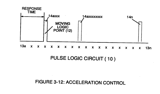
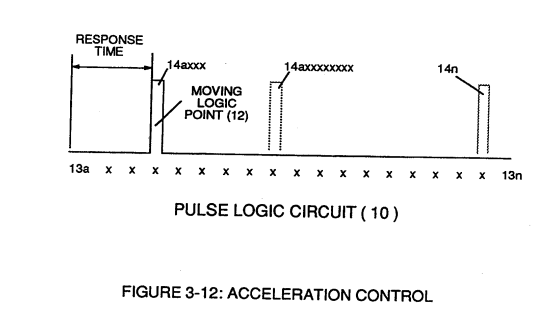
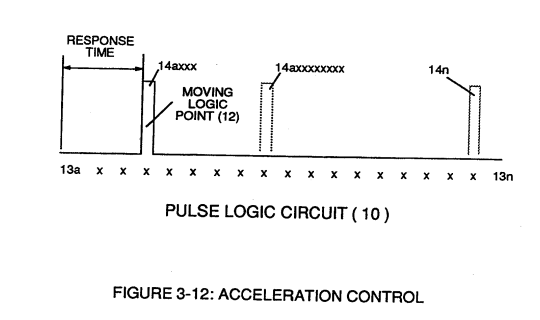
… 7) by linearly moving (forward and/or reverse direction) "low" logic state signal (12) in a array of "high" logic state output signals (13a xxx 13n), as further illustrated in Figure (3-8) and Figure (3-12).
-
Figure (3-12)
-
As signal output (15) of figure (4) (14a xxx ... 12 ... xx14n) is being received by acceleration control circuit (30) of Figure (3-5) as to Figure (3-12), circuit (30) converts incoming time-response signal (14a xxx ... 12 ... xx14n) into a variable time-base unipolar pulse (16), as shown in Figure (3-8).
-
Circuit (30) continues to increase pulse width (17axxxx) of Figure (3-8) as the monitored (detected by < scanning) toggling-time (14a xxxx ... 12) increases when logic-point (12) moves farther away from start-position (9a) to stop-position (9n), as further shown in Figure (3-13) as to Figure (3-12).
-
Figure (3-12)