patent · US6084173
Method and apparatus for the generation of charged carriers in semiconductor devices
4 July 2000
Page 1 — bibliographic record
United States Patent (19) 11 Patent Number: 6,084,173 DiMatte0 (45) Date of Patent: Jul. 4, 2000 54 METHOD AND APPARATUS FOR THE 56) References Cited GENERATION OF CHARGED CARRIERS IN U.S. PATENT DOCUMENTS SEMCONDUCTOR DEVICES a 5,651,838 7/1997 Fraas et al. ............................. 136/253 76 Inventor: Robert Stephen DiMatteo, 85 Walnut Primary Examiner Kathryn Gorgos Ct., Stoughton, Mass. 02072 ASSistant Examiner Thomas H. Parsons
Attorney, Agent, or Firm-Rines and Rines 21 Appl. No.: 08/902,817 57 ABSTRACT 22 Filed: Jul. 30, 1997 A technique for enhancing the generation of carriers (ex. (51) Int. Cl. ............................................... H01L 35/00 electrons and/or holes) in Semiconductor devices Such as photovoltaic cells and the like, receiving radiation from a heated Surface, through the use of micron juxtaposition of 52 U.S. Cl. ........................... 136/201; 136/223; 136/253 the Surface of the device and the heated Surface and with the gap thereinbetween preferably evacuated.
58 Field of Search ..................................... 136/223, 200, 136/201, 203, 205, 253 15 Claims, 1 Drawing Sheet
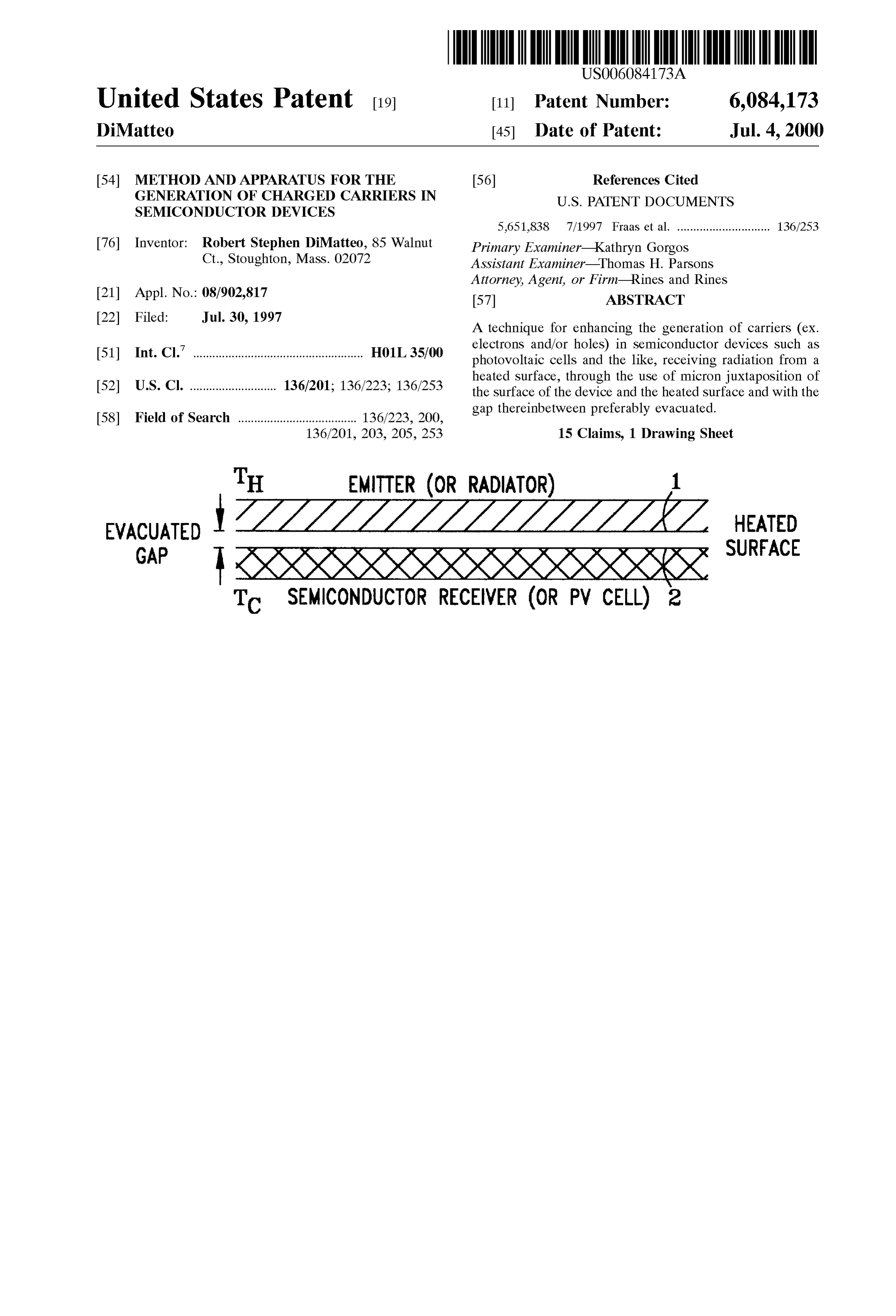
TH EMITTER (O R RADATOR) 1 cut ZZZZZZZZZZZZZZZZYZ HEATED
GAP
XXXXXXXXXXXXXXX
To SEMICONDUCTOR RECEIVER (ORPV CELL) 2
Page 2
Drawing sheet — no readable text.
Page 3
METHOD AND APPARATUS FOR THE than at larger distances, and that the magnitude of this effect GENERATION OF CHARGED CARRIERS IN increases Sharply with decreasing distance. Examples of SEMCONDUCTOR DEVICES Such experiments are Cravalho, E. G. et. al., November 1967, “Effect of Small Spacings on Radiative Transfer
BACKGROUND OF THE INVENTION Between Dielectrics”, Journal of Heat Transfer, 1. Field of the Invention pp.351–358; Hargreaves, C. M., 1973, “Radiative Transfer Between Closely Spaced Bodies”, Philips Res. Reports
The present invention relates to the general area of Supplement generating carrierS Such as electrons and holes within Semi August 1978,No.5, pp. 1-80; and Kutateladze, S. S., et. al., “Effect of Magnitude of Gap Between Metal conductors by the action of incident radiation, being more Plates on their Thermal particularly concerned with radiation emanating from heated Temperatures”, Soy: Phys. Dokl.Interaction
at Cryogenic
Surfaces, and, in an important application, to the enhance of magnitude increase with very Small or “microScale” ment of Such generation within photovoltaic devices and the spacings were theoretically predicted by Polder, D. et. al., like, due to the close proximity of the heated Surface. November 1971, “Theory of Radiative Heat Transfer 2. Description of the Prior Art 15 between Closely Spaced Bodies”, Physical Review B, Vol. 4, In a common photovoltaic cell, a Semiconductor p-n No. 10, pp.3303-3314 and Levin, M. L. et al., 1980, junction is formed close to the Surface of the Semiconductor “Contribution to the Theory of Heat Exchange Due to a material that forms the cell. When photons emitted by a light Fluctuating Electromagnetic Field”, Soy: Phys. JETP Vol. 6, Source Such as the Sun impinge on the cell Surface, electron pp. 1054–1063.
hole pairs are created. These electron-hole pairs are sepa Underlying the present invention, is my novel conceptual rated by the Space-charge potential that is a consequence of insight and discovery that these previously unrelated tech the p-n junction. The net result is a DC current. Thermo nologies of thermophotovoltaic energy conversion and of photovoltaics operate in a similar manner except that, Small spacing radiative heat transfer Systems could Syner instead of a light Source, a Surface at a higher temperature gistically be combined in Such a manner as to enhance the than the Semiconductor material acts as the Source of pho 25 generation of Semiconductor carriers (electrons and holes) in tons. In this case, thermal radiation is the mechanism of Semiconductor devices Such as photovoltaic cells and the energy transfer and the temperature of the emitting Surface like, receiving radiation, Such as photons, from a heated which dictates the Spectral composition of the radiation must Surface, through the use of very Small gap juxtaposition of be matched to the material and electronic properties of the the Surfaces of the device and the heated Surface. Semiconductor Such as its bandgap in order to optimize conversion efficiency. SUMMARY OF THE INVENTION Prior thermophotovoltaic devices and systems have been A primary object of the invention accordingly, is to designed Such that the distance between the emitting Surface provide a new and improved method of enhancing the and the cell Surface is large relative to the characteristic wavelength of the thermal radiation. Hence, the thermal 35 generation of carriers (ex. electrons and/or holes) in Semi conductor devices and near their Surfaces, receiving radia radiation transfer is characterized by the Stefan-Boltzman tion from a heated Surface, through the use of very Small gap Law and its spectral composition by Planck's law. ("microScale') juxtaposition of the Surface of the Semicon MicroScale Radiative Heat Transfer ductor Surface or device and the heated Surface. Turning now from the field of Semiconductor devices, A further object is to provide an improved thermophoto including photovoltaic cells and the like, to the general field 40 Voltaic System.
of radiative heat transfer, in the classical theory of radiative heat transfer, the radiated power per area and per interval of Other and further objects will be explained hereinafter wavelength of a flat surface in thermal equilibrium with its and will be more particularly delineated in the appended Surrounding is given by Planck's Law. Integration of claims.
Planck's Law over all wavelengths yields the Stefan 45 In Summary, from one of its broader aspects, the invention Boltzman Law for black surfaces. Similarly, this law gov embraces a method of enhancing the generation of carriers erns the exchange of energy between two black Surfaces. in a Semiconductor near its Surface receiving radiation from Planck's law predicts that a large portion of the radiative a heated Surface, that comprises, placing the Surfaces in energy at a given temperature of the radiating body will be juxtaposition, and adjusting the Space therebetween to around the wavelength of greatest spectral intensity "lamb 50 micron Scale Separation.
damax'. “Lambdamax' is predicted by the Wien Displace Preferred and best mode designs and implementations ment Law. At shorter wavelengths the power falloff is very will later be detailed.
rapid whereas at wavelengths greater than lambdamax the falloff is much more gradual. At lower temperatures, lamb BRIEF DESCRIPTION OF THE DRAWING damax occurs at longer wavelengths. 55
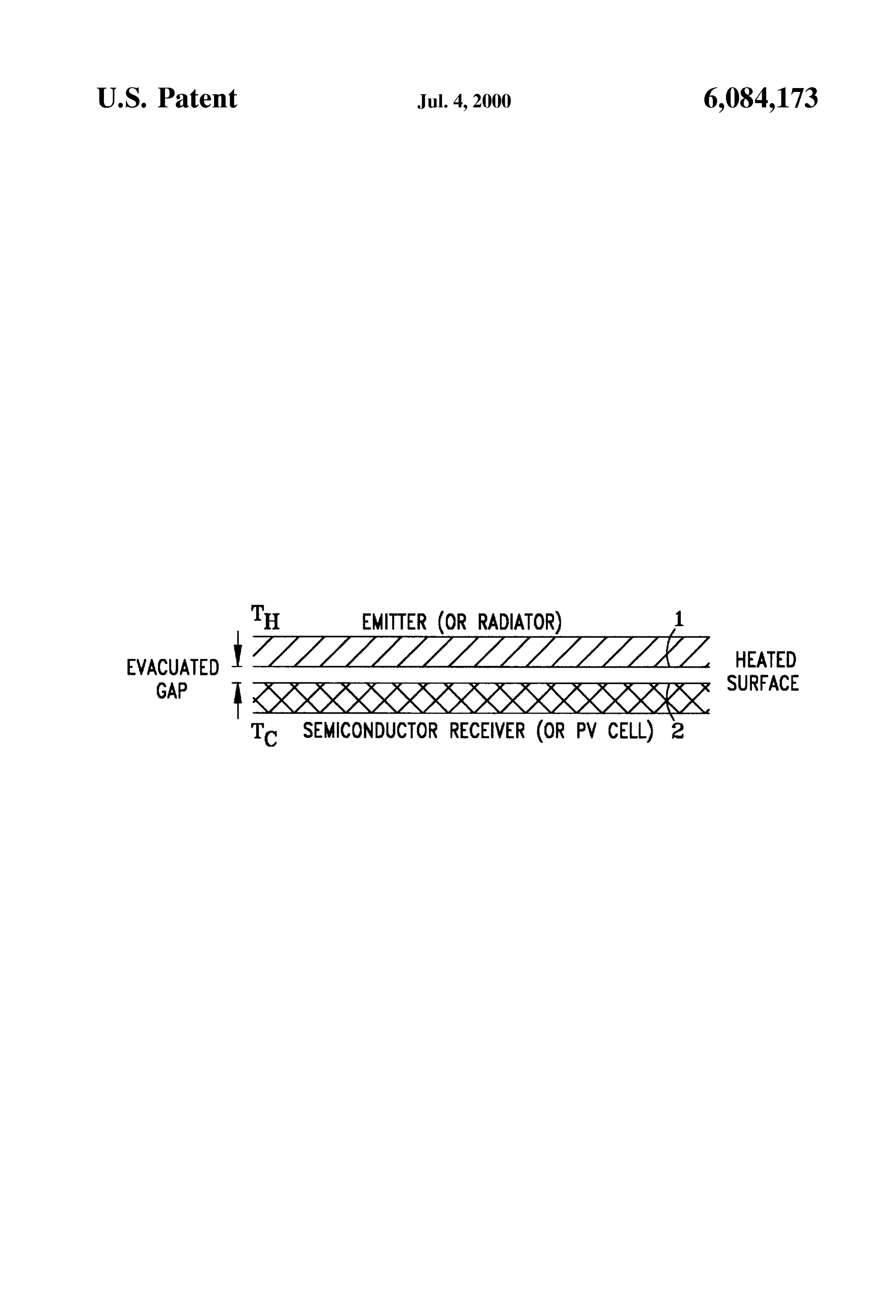
In the above classical theory, it is assumed that the The schematic FIGURE illustrates the novel principles of distances between radiating Surfaces all large compared to the invention as applied to an exemplary application of a thermophotovoltaic device.
the wavelengths of the energy involved. Planck himself imposed this condition on his derivation. Over the last DETAILED DESCRIPTION OF THE Several decades, a Small Segment of radiative heat transfer 60 INVENTION theory and experimentation has developed wherein the
Spaces between radiating Solids are on the order of and The invention will now be described in connection with Smaller than the characteristic wavelengths of the radiation the accompanying drawing.
eXchanged. There is experimental evidence to show that the Referring to the drawing, a heated Surface emitter of energy exchange between two Surfaces (dielectric to dielec 65 radiation, including photons, is Schematically shown at 1 in tric or metal to metal) separated by a distance of the same the form of a Substantially planar hot Surface at temperature order as the wavelength or less can be Several times larger T, juxtaposed in accordance with the present invention, in
Page 4
very close proximity to a Substantially parallel Surface 2 of generation of electrical currents in response to the radiation a Semiconductor receiver of the radiation, Such as a photo coupled through the gap.
voltaic cell of relatively cool temperature of T. Cell current 2. A method as claimed in claim 1 wherein the gap spacing collection contacts and grid (not shown) would be provided is adjusted to the order of from about 0.01 to 100 microns. in the bottom or back Surface or recessed from the front 3. A method as claimed in claim 1 wherein a Semicon active Surface of the cell. ductor Surface is provided with photovoltaic properties, and The enhanced Synergistic effect of the invention in terms maintained relatively cool with respect to the heated Surface. of Significant increases in carrier generation in response to 4. A method as claimed in claim 3 wherein each of the the incident radiation from heated surface 1 is achieved by photovoltaic and heated Surfaces are formed as Substantially effecting the above mentioned critical close proximity of the planar Surfaces, placed in juxtaposition Substantially in Surfaces 1 and 2 with a micro gap, having the well-known parallel.
inherent properties of being both thermally insulative and 5. A method as claimed in claim 4 wherein, prior to the capable of transmitting or coupling radiation with little loSS, juxtaposition placing, a step is performed of patterning one (Evacuated Gap) on the order of 0.01 microns up to the order 15 or both of the juxtaposed Surfaces. of about 1 micron and in Some cases of longer wavelengths 6. A method as claimed in claim 4 wherein, prior to the (as in cryogenic applications and the like) even up to the juxtaposition placing, a Step is performed of varying the order of 100 microns, 0.01-20 microns being a preferred properties of one or more of the Surfaces in dimensions range for most applications. orthogonal to and parallel to Said Spacing. The fine adjustment of the crucial micron range Separation 7. The method as claimed in claim 1 wherein, prior to said gap between the Surfaces 1 and 2 may be controlled by Such emitting of radiation and Said adjusting, a step is performed devices as piezoelectric controlled leveling Stages or the like of providing Said Semiconductor Surface with photovoltaic properties.
such as the Model 8095 of New Focus Corporation.
In View of the very Small gap, moreover, Vibration isola of 8.theTheelectrical method claimed in claim 1 wherein the magnitude tion may be required as by conventional isolation tables and 25 adjustment of the currents gap.
generated is controlled by the the like.
While the invention has been described in connection 9. The method of claim 8 wherein the energy enhance with the example of a photovoltaic Semiconductor device, it createsachieved ment energy by the Submicron/micron gap adjustment
Stimulation that is converted into the is evident that the carrier enhancement effect from close juxtaposition of a Semiconductor Surface and a heated Sur enhanced generation of the electrical currents. face is generically applicable and useful. 10. The method of claim 9 wherein the relatively cool Surface is a photovoltaic Surface and the enhanced genera
Instead of flat Surfaces, patterns may be etched or other tion of the electrical currents manifests itself in the power wise formed into three-dimensional forms (channels, output of the photovoltaic Surface.
islands, etc.) to tailor the electromagnetic spectrum of the 11. A method of enhancing the generation of carriers in a radiant energy being transferred to the juxtaposed Semicon 35 Semiconductor Surface receiving radiation from a heated ductor Surface. There may then be a natural progression Surface, that comprises emitting radiation from a heated from one dimension, MTPV, ie. controlling the distance Surface of temperature T, coupling the radiation through an between two Surfaces, to three dimensions wherein in addi evacuated gap for reception by a relatively cool Semicon tion to the MicroScale Spacing, the properties of the Surfaces ductor Surface maintained attemperature T, where TZT, as a function of the two lateral dimensions are also con 40 and adjusting the Spacing of the gap to the order of trolled. In Summary, if X and y are in the plane of the Emitter SubmicronS/microns to achieve an enhanced increase in the and Receiver chip Surfaces and Z is perpendicular to them, Semiconductor generation of charged carriers in response to then the degrees of freedom are: Z between the chips, Z the radiation coupled through the gap, wherein one or both within one or both chips, X and y within one or both chips, of the heated and Semiconductor Surfaces is formed for and X and y of one chip relative to the other. 45 tailoring the Spectrum of the emitted radiation coupled Semiconductors include Si and binary, ternary, and qua through the gap.
ternary compound Semiconductors including InAS, InGaAS, 12. The method as claimed in claim 11, wherein the and InCaAsSb and others. forming is provided along one or more of the X, Y and Z The heated Surface, moreover, may not only involve axes of either or both Surfaces.
lattice and carriers at the Same temperature, but also condi 50 13. The method as claimed in claim 11 wherein, prior to tions where the carriers are at a hotter temperature than the Said adjusting, providing either or both of the Surfaces with lattice (“hot electrons') as through absorption of electro one of patterns, channels, islands and three-dimensional magnetic energy. forms.
Further modifications will also occur to those skilled in 14. A method of enhancing the generation of carriers in a this art, and as Such are considered to fall within the Spirit 55 Semiconductor Surface receiving radiation from a heated and Scope of the this invention as defined in the appended Surface, that comprises, emitting radiation from a heated claims. Surface of temperature T, coupling the radiation through an What is claimed is: evacuated gap for reception by a relatively cool Semicon 1. A method of enhancing the generation of electrical ductor Surface maintained attemperature T, where TZT, currents in a conductive or Semi-conductive Surface receiv 60 and adjusting the Spacing of the gap to the order of ing radiation from a heated Surface, that comprises, emitting SubmicronS/microns to achieve an enhanced increase in the radiation from a heated Surface of temperature T, coupling Semiconductor generation of charged carriers in response to the radiation through an evacuated gap for reception by a the radiation coupled through the gap, wherein the relatively cool conductive or Semi-conductive Surface main Submicron/micron Spacing is adjusted by controlling the tained at temperature T, where TZT, and adjusting the 65 leveling of the Surfaces.
spacing of the gap to the order of SubmicronS/microns to 15. A method of enhancing the generation of carriers in a achieve an enhanced increase in the relatively cool Surface Semiconductor Surface receiving radiation from a heated
Page 5
S 6
Surface, that comprises, emitting radiation from a heated Semiconductor generation of charged carriers in response to Surface of temperature T, coupling the radiation through an the radiation coupled through the gap, wherein the gap is evacuated gap for reception by a relatively cool Semicon- isolated from vibration.
ductor Surface maintained at temperature T, where TZT, and adjusting the Spacing of the gap to the order of 5
Submicrons/microns to achieve an enhanced increase in the k . . . .

Provenance
- Collection
- Cited prior art
- Original PDF
- patentimages.storage.googleapis.com →
- Filed
- 1997-07-30
- Pages
- 5
- Method
- pdftotext (the PDF's own text layer) + pdftoppm 300dpi page scans
- Source
- Google Patents bibliographic record
- Granted
- 2000-07-04
- Inventors
- Robert Stephen DiMatteo
- Transcribed from
- patentimages.storage.googleapis.com →