patent · US20050189011A1
Gas specie electron-jump chemical energy converter
1 September 2005
Page 1 — bibliographic record
(19) United States (12) Patent Application Publication (10) Pub. No.: US 2005/0189011 A1
Zupper0 et al. (43) Pub. Date: Sep. 1, 2005 (54) GAS SPECIE ELECTRON-JUMP CHEMICAL (60) Provisional application No. 60/290,058, filed on May ENERGY CONVERTER 10, 2001.
(76) Inventors: Anthony C. Zuppero, Pollock Pines, Publication Classification CA (US); Jawahar M. Gidwani, San
Francisco, CA (US) (51) Int. Cl. ................................................ H01L 31/00 (52) U.S. Cl. ............................................ 136/243; 136/252
Correspondence Address:
BAKER & MCKENZE LLP
805 THIRDAVENUE - 29TH FLOOR (57) ABSTRACT
(21) Appl. No.: 10/625,801 An apparatus and method for extracting energy is provided. In one aspect the method includes using chemical reactions (22) Filed: Jul. 23, 2003 to generate vibrationally excited molecules, Such as high quantum-number-vibrationally-excited gas molecules in a
Related U.S. Application Data region. The vibration energy in the vibrationally excited molecules is converted into hot electrons when the excited (60) Continuation of application No. 10/142,684, filed on molecules contact a conductor. A geometry is provided So May 10, 2002, now Pat. No. 6,649,823, and which is that the excited molecules may travel, diffuse or wander into a continuation-in-part of application No. 10/038,257, a conductor before loosing a useful fraction of the vibra filed on Oct. 24, 2001, now Pat. No. 6,700,056, which tional energy. Optionally, the generating and the converting is a continuation of application No. 09/589,669, filed process may be thermally Separated, at least in part. The on Jun. 7, 2000, now Pat. No. 6,327,859, which is a Short lived hot electrons are converted into longer lived division of application No. 09/304,979, filed on May entities Such as carriers and potentials in a Semiconductor, 4, 1999, now Pat. No. 6,114,620. where the energy is converted into a useful form.
MvMyvrwawasawwuavasyuvau-Wussyswaywk wasyawasak wn www.wawayww.wawha WyMsawrassr. Navy MWAWAws
Page 2
Drawing sheet — no readable text.
Page 3
Drawing sheet — no readable text.
Page 4
Drawing sheet — no readable text.
Page 5
Drawing sheet — no readable text.
Page 6
Drawing sheet — no readable text.
Page 7
Drawing sheet — no readable text.
Page 8
Drawing sheet — no readable text.
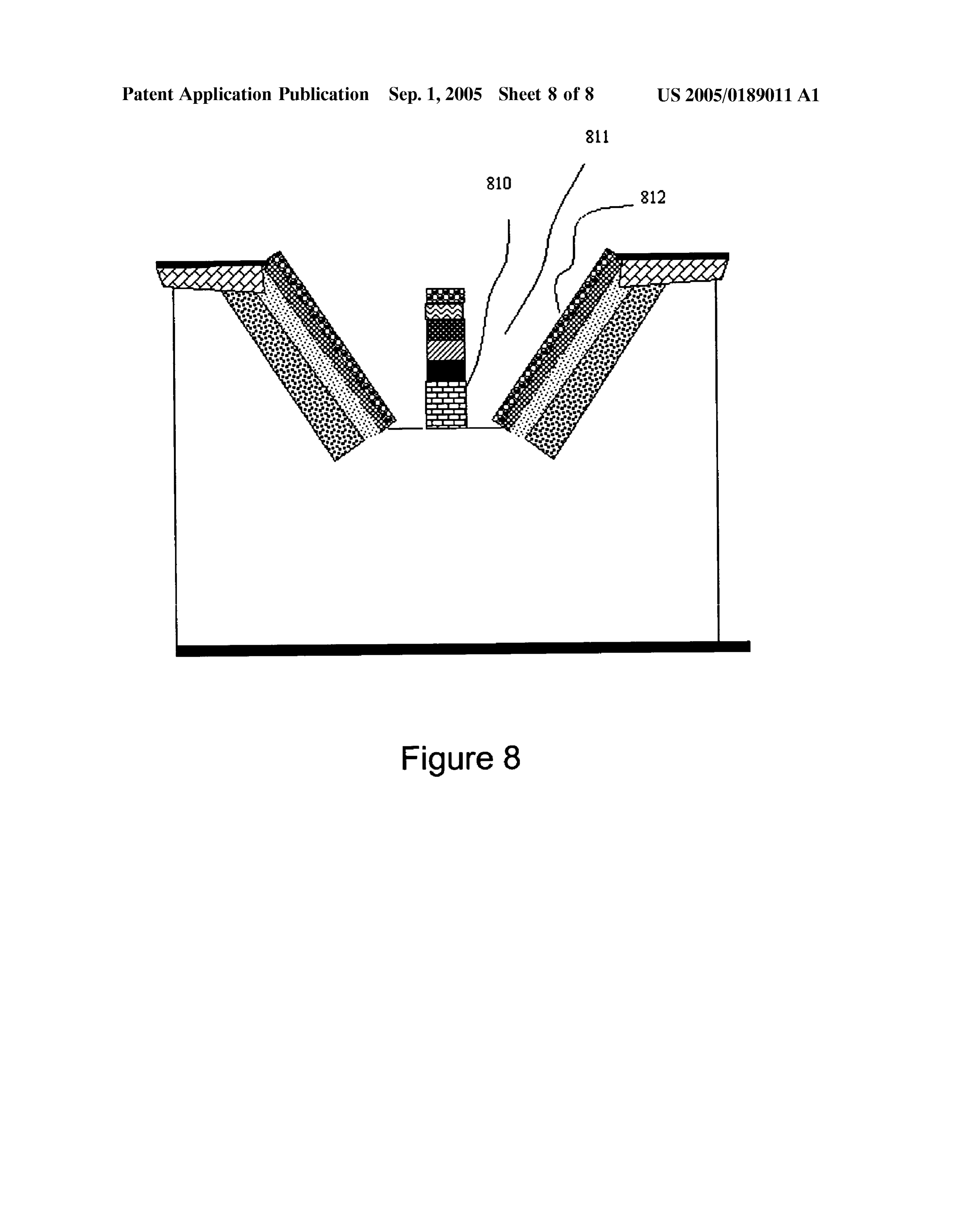
Page 9
Drawing sheet — no readable text.
Page 10
US 2005/0189011 A1 Sep. 1, 2005
GAS SPECIE ELECTRON-JUMP CHEMICAL catalysts, injection of autocatalysts, or other means. A Sub ENERGY CONVERTER Stantial fraction of the excitation energy may be transferred to an energetic electron in a metal when the excited Specie
CROSS REFERENCE TO RELATED comes in contact with the metal. See Huang, Yuhui, Charles APPLICATIONS T. Rettner, Daniel J. Auerbach, Alec M. Wodtke, Science, 0001) This application claims the benefit of U.S. Provi Vol. 290, 6 October 2000, pp 111-113, “Vibrational Promo tion of Electron Transfer.’ sional Patent Application No. 60/290,058, filed on May 10, 2001, which application is incorporated herein by reference 0008 According to results of experiments, vibrationally in its entirely. This application is a continuation-in-part of excited anions may absorb an electron and re-emit an
2001. U.S. patent application Ser. No. 10/038,257 is a tation energy. By analogy, cations may emit an electron and continuation of U.S. patent application Ser. No. 09/589,669, reabsorb it, emitting a hole into the lattice, with the hole filed on Jun. 7, 2000, now U.S. Pat. No. 6,327,859. U.S. carrying the energy. The electron or hole is the hot carrier. patent application Ser. No. 09/589,669 is a divisional of U.S. 0009 Recent experimental observations and theoretical patent application Ser. No. 09/304,979, filed on May 4, developments in Surface Science confirmed that even rela 1999, now U.S. Pat. No. 6,114,620. tively weakly electronegative gas molecules Vibrating with TECHNICAL FIELD OF THE INVENTION an energy almost Sufficient to break their chemical bonds (vibration quantum number in excess of order 15) can 0002 The invention relates generally to a method and deposit a majority of the vibration energy into an electron of device to convert chemical reaction energy directly into the metal Surface during a single, brief contact (of order 0.1 electric power, and more specifically to a method and device picoSeconds) with that Surface. Research and observations to generate vibrationally highly excited reaction products asSociated with understanding this observation Support the and to convert the product energy directly into useful forms, theory of prompt, multi-quantum energy transfer to a single Such as electricity, hot electrons in a metal Surface, long electron from a vibrationally excited chemical Specie. lived carriers in a Semiconductor, radiation or coherent 0010 Typically, more than half of the vibrational mode radiation.
energy will be transferred directly into an electron of the
BACKGROUND OF THE INVENTION metal Surface with an energy greater than approximately 5 vibrational quanta. The result is that an electron in a metal 0003. The fuel cell is a clean and efficient electrochemi Surface may carry away a Substantial, useful fraction of the cal energy conversion method that typically converts chemi Vibrationally excited molecule energy as a hot electron, also cal reaction energy of reactant gases directly and efficiently referred to as a hot carrier.
into electricity. The power per mass or per Volume exhibited 0011. In the metal, the hot electron may travel into a by a fuel cell System, however, is typically at least an order Semiconductor. The hot electron becomes converted into an of magnitude lower than that of mechanical engines. Further, excitation or potential difference in the Semiconductor where the Volume needed for a fuel cell using liquid, Storable fuels it may be converted into other useful forms Such as an to generate the power of a given battery is typically signifi electrical potential driving a current in an external circuit, an cantly larger than that of the battery. This means that the inverted population of Semiconductor excitations, or hot present form of fuel cells cannot replace the battery regard carriers transported to other locations for use. less of the fuel cell efficiency, because there is no room for fuel. 0012. The hot electron may be converted into a potential 0004. In addition, the type of fuel cell with the highest in a semiconductor. For example, U.S. Pat. No. 6,222,116 known power per mass, the Solid oxide fuel cell, operates at collectS Such hot electrons directly without mechanical temperatures of 600 to 800 Celsius. Operation at this tem means, and converts them directly into electricity when the perature presents materials problems as a result. In principle, Vibrationally excited chemical product specie is formed on or within a few molecule dimensions of the reaction Surface this fuel cell would exhibit the power density required to of its device. The device described in this patent generates operate in the volume of a battery it would displace. Thermal useful electricity by causing the reactions rates to be Suffi issues, however, have dominated and prevented realization ciently high to energize the Semiconductor converter into of this goal. maintaining a useful forward bias. 0005 The alternative to a high performance fuel cell is a 0013 A removal of spent reaction products through des rotating mechanical device. However, mechanical engines orption from a hot-electron collection Surface may enhance generating electricity must typically use coil and magnet this high reaction rate. De-energized molecules desorbing devices to convert mechanical energy into electrical energy may leave behind a clean Site for more reactions. Allowing and are therefore relatively heavy, with power densities leSS these de-energized molecules to migrate away from the than 2 watts per gram. conducting Surface may initiate further reaction with more 0006 Therefore, there is a need to have a method and oxidizers and fuels.
System for converting chemical energy directly and effi 0014. Accordingly, there is a need to have a method to ciently into electricity and to have methods that do not produce vibrationally highly excited Specie directly from require high temperatures and materials and that do not chemical reactions and where the conversion of the electri require relatively heavy mechanical devices. cal energy of the excited Specie may take place at a location 0007. A chemical reaction typically creates highly vibra different from in the thermal sense and separated from the tionally excited Specie, which reaction may be Stimulated by creation of the excited Specie. Further, there is a further need
Page 11
US 2005/0189011 A1 Sep. 1, 2005
to have reactions take place in a Volume, not just a Surface, gized molecules and a collection region collects the energy to increase the rate of reaction compared to that on a Surface. from the energized molecules,
SUMMARY OF THE INVENTION 0022 FIG. 2 shows a schematic cross section of the energy converter portion of an apparatus using the p-n 0.015. In one aspect, a method is provided to use chemical junction option to generate a useful electrical potential from reactants to produce vibrationally excited gas molecules in energized molecule energies, a reaction volume or region, and to extract a Substantial 0023 FIG. 3 shows a schematic cross section of the fraction of energy, for example, as hot electrons in a con energy converter portion of an apparatus using the Schottky ducting Surface, and to convert the energy, Such as hot junction option to generate a useful electrical potential from electrons, into useful forms of energy. energized molecule energies, 0016. The method includes using chemical reactions to 0024 FIG. 4 shows a schematic cross section where a generate vibrationally excited molecules Such as high quan reaction region generates the energized molecules, a collec tum number Vibrationally excited gas molecules. The vibra tion region collects the energy from the energized molecules tion energy in the vibrationally excited molecules is con and uses a Schottky junction to generate electricity; verted into hot electrons when the excited molecules contact a conductor. A geometry Such as a gas reaction region with 0025 FIG. 5 shows a schematic cross section of a device dimensions of order Several molecular collision mean free that Stores excitations created by excited molecules, paths and bounded in part by a conducting Surface is 0026 FIG. 6 shows a schematic cross section of a device provided So that the excited molecules may travel, diffuse or that converts excitations created by excited molecules into a wander into a conductor before loosing a useful fraction of population inversion;
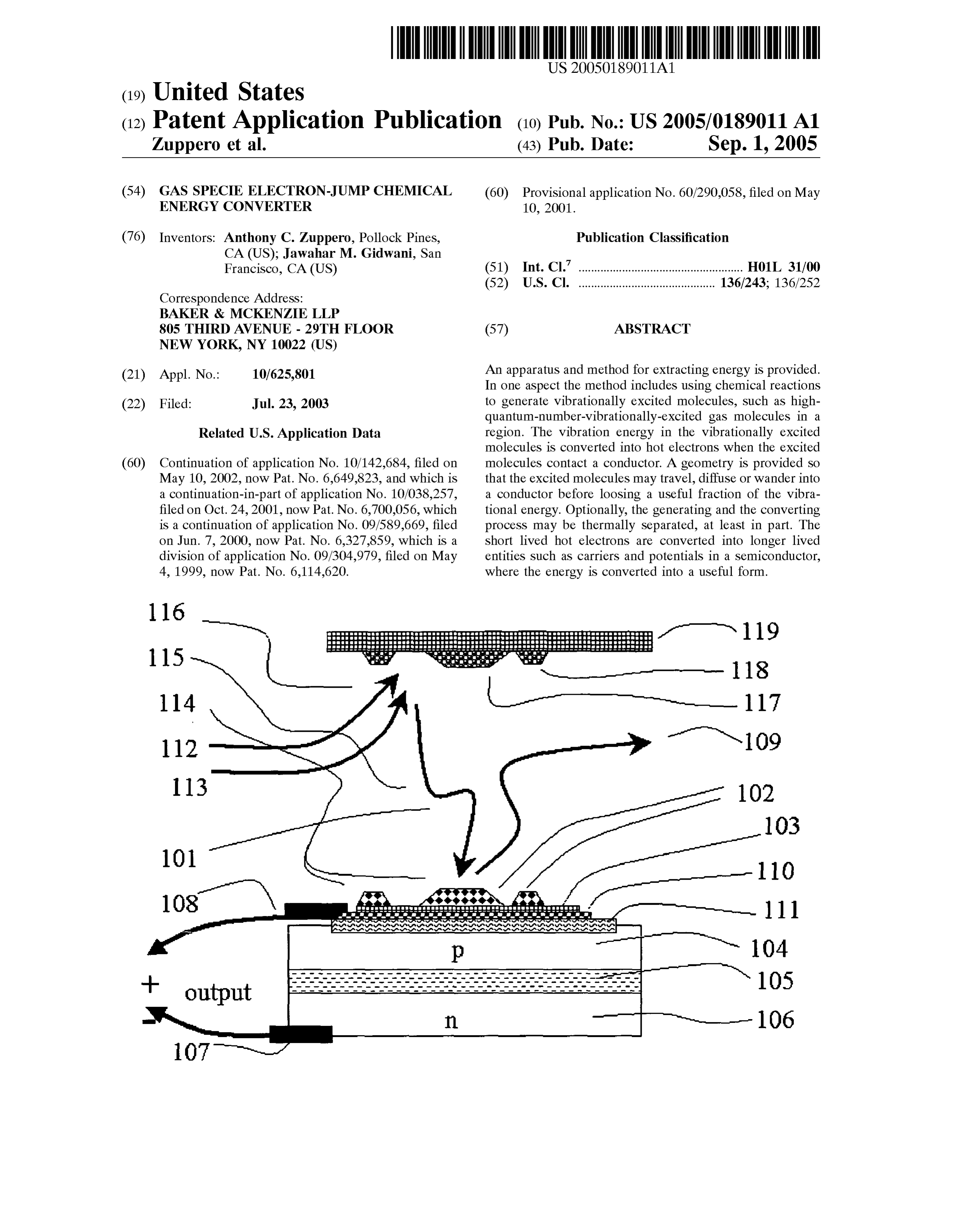
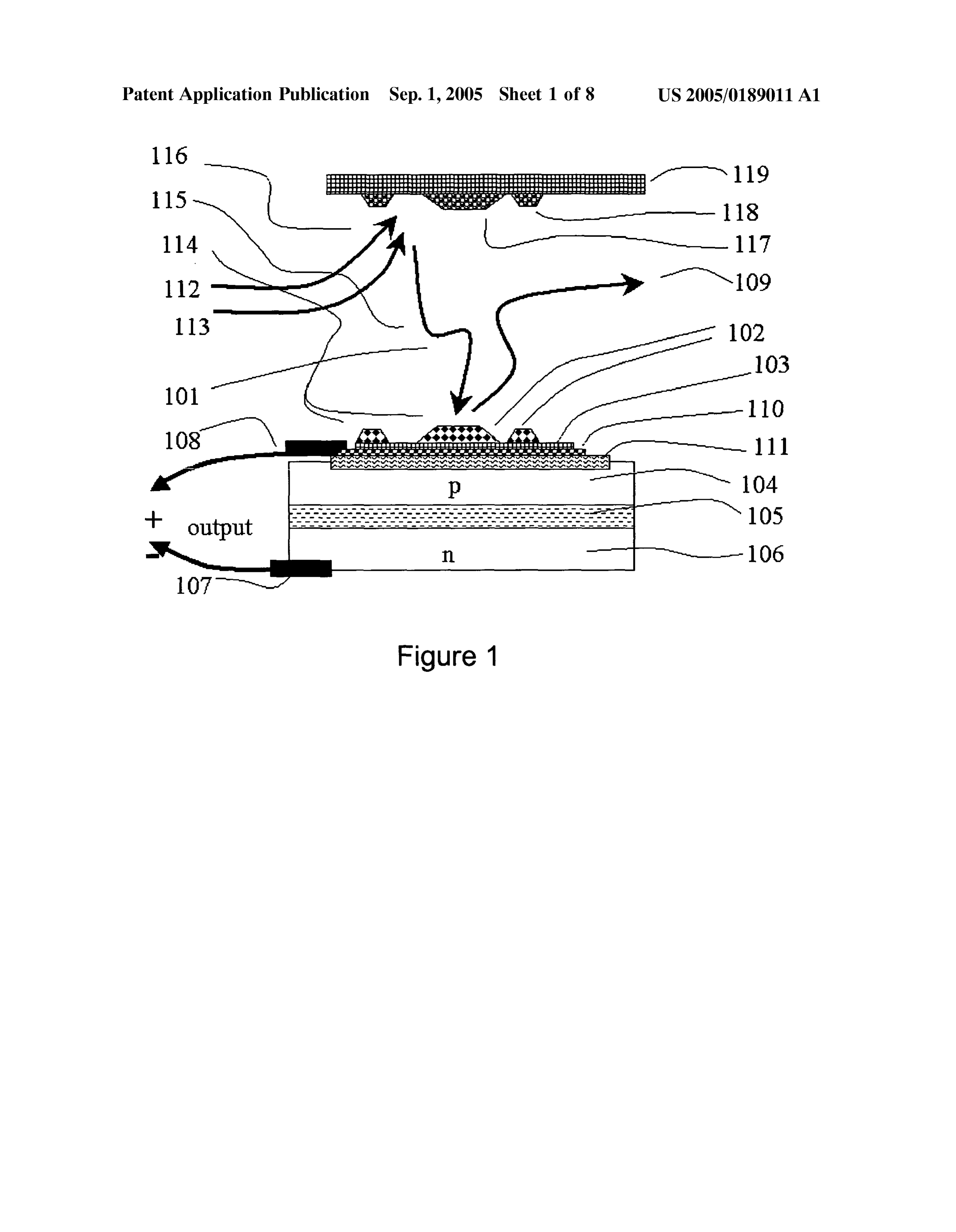
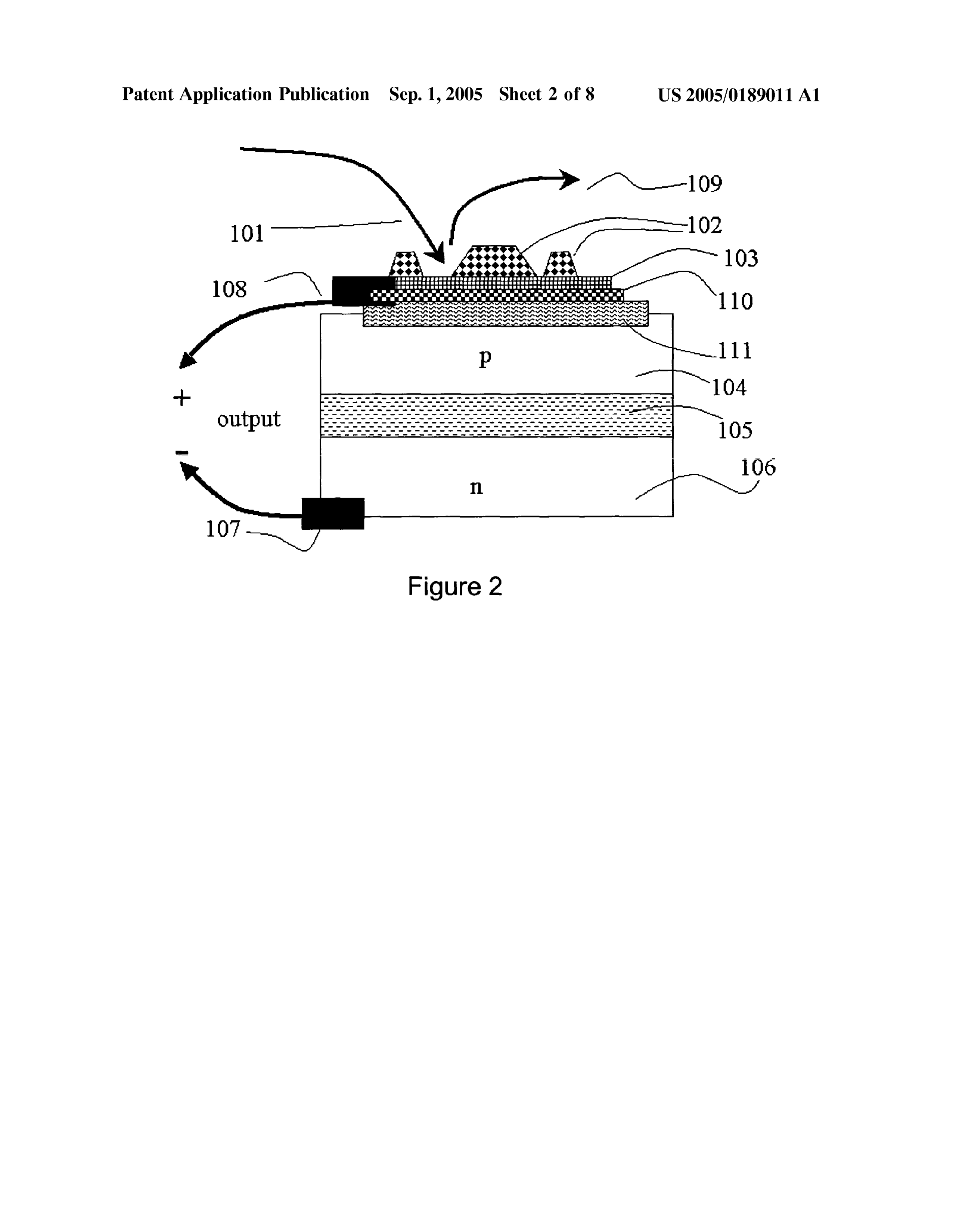
the vibrational energy. Optionally, the generating and the converting process may be thermally Separated, at least in 0027 FIG. 7 shows a schematic cross section of a device part. The short lived hot electrons are converted into longer with Separate fuel and oxidizer channels, Separated reaction lived entities Such as carriers and potentials in a Semicon and collection regions and thermal isolation; and ductor, where the energy is converted into a useful form. 0028 FIG. 8 shows a schematic cross section of a device 0.017. In another aspect, an apparatus for generating illustrating thermal barriers and Separated reaction and col energy provided includes a reaction region where the reac lection regions.
tants, for example, fuel and oxidizer, undergo chemical reactions that produce highly vibrationally excited mol DETAILED DESCRIPTION OF THE ecules. Exhausts produced in the reaction are allowed to INVENTION leave the System. A reaction region may be close enough to 0029. In one aspect, the method and apparatus provided the collection Surface So that the excited products do not enhance the peak power and the rate of energy conversion loose a Substantial fraction of their energy before reaching and further enhance the desorption of exhaust and contami the collection Surface. A collection Surface may include a nation products from the conducting Surface. The method, in Surface Such as a conductor near or on which excited products transfer energy to a hot electron or carrier (electron one aspect, includes choosing catalysts with relatively low or hole). A conversion region may be in contact with the affinity for exhaust products. Such catalysts include plati collection Surface, where the hot electron or carrier is num, palladium and related catalysts have shown this prop converted into a useful form, Such as a potential in a erty with respect to hydrogen and alcohol combustion. Semiconductor Sustained by Separated carriers. This conver 0030. In another aspect, the method includes bringing Sion region may be at least partly isolated at least thermally fuel and oxidizer into the reaction region and permitting from the reaction region. exhaust products to leave the reaction region. Exhaust products may migrate and diffuse away. One way to allow 0.018 Yet in another aspect, the method may include the exhaust products to migrate and diffuse away includes transferring reaction product excitations Such as multiple flowing gaseous reactants over the reaction Surface and quantum change of energy of a dipole active State of a letting the exhaust products leave the Surface into the gas Vibrational State, which are a type of excitation of the flow. In another aspect, the apparatus provided may be energized chemical products. designed to generate a Single, one time pulse of power, in 0.019 Further features and advantages of the invention as which case the exhaust products need not leave the reaction well as the Structure and operation of various embodiments region.
of the invention are described in detail below with reference 0031. The method provided may include using energized to the accompanying drawings. In the drawings, like refer molecules that have migrated through a gas reaction volume ence numbers indicate identical or functionally similar ele to a conducting Surface. When the energized molecules mentS.
interact with the conducting Surface they give up a Substan
BRIEF DESCRIPTION OF THE DRAWINGS
tial fraction of the chemical vibration energy to the con ducting Surface in the form of an energetic, ballistic electron.
0020 Embodiments of the invention will now be The conducting Surface is formed Sufficiently thin to permit described, by way of example only, with reference to the the ballistic electron to migrate and diffuse directly into a accompanying drawings in which: Semiconductor Substrate. The Semiconductor converts the electron energy into a Storable, useful form with a much 0021 FIG. 1 shows a schematic cross section of an longer lifetime (e.g. picoseconds or longer) than the lifetime apparatus where a separated reaction region generates ener of a ballistic electron (e.g. 0.01 picoSeconds). Typically, the
Page 12
US 2005/0189011 A1 Sep. 1, 2005
semiconductor is formed into a diode and the useful form of Stimulators and by using reaction geometries that form energy is the generation of electricity as a forward bias in the Vibrationally excited gaseous molecules at any locations diode. where they may readily migrate and diffuse to a conducting 0032. A conducting surface may include catalysts and/or Surface before loosing a Substantial amount of excitation. catalyst metals So that reactions on the catalyst continuously 0039. During operation, known stimulation devices such remove adsorbates and provide clean metal with which as catalysts, reaction Stimulator methods, and additives may Vibrationally excited gas Specie may interact. Additives be used to produce vibrationally excited Specie after reac Supplied with fuel and/or oxidizer may Supply the catalysts. tants enter a region of reaction. Stimulator methods include Oxidizing reactions are known to be effective to remove using one or more catalysts, catalysts on a reaction Surface, adsorbed, unreacted Specie. Nearly all fuel-air reactions are electric discharges, gliding electric discharges, optical and oxygen rich, tending to favor or permit favoring Such photolytic methods, optical devices, and injected catalysts, oxidizing reactions for Surface Self cleaning. catalytic or autocatalyst materials. The Stimulation device 0033. A conducting surface may be considered to be may generate free radicals as Stimulators, for example, using conducting even when a monolayer of reactive adsorbate electrical or optical energy.
resides on that Surface. Such adsorbates include oxygen and 0040 Since most stable chemical reactions are activated fuel molecules. Generally, a fraction of a monolayer of oxide (having a potential energy barrier that keeps reactants apart), may form on catalyst conducting Surfaces. the Stimulation device may provide the activation energy 0034. In one aspect, the apparatus provided may use fuel using electrical means. The apparatus provided recovers a and oxidizer to create the energized molecules in the vicinity fraction of that energy.
of a conducting Surface. In addition, highly vibrationally 0041 Gaseous chemical reactions in a volume of fuel and excited Specie may be generated in the vicinity of a con oxidizer mixtures produce gas products whose initial State is ducting Surface by reaction of fuel, Such as methanol, one where the energy is concentrated Substantially in the hydrogen, or partially oxygenated and complex hydrocar Vibration mode. The Vibration modes of a gas typically have bons, and an oxidizer, Such as air. Fuels from any one of any lifetimes of 10's to 10,000's of gas kinetic collisions (for reducing material or electron donor may be chosen, includ non-resonant interactions), and the pre-equilibrium mean ing but not limited to hydrogen, hydrocarbons, complex free path for typical hydrocarbon - air reaction products are hydrocarbons, alcohols Such as methanol, ethanol and pro of order 50 to 200 nanometers in the gas. This means that panol, carbohydrates, partially oxygenated hydrocarbons, reaction channels to take advantage of this mean free path diesel fuel, kerosene, Volatized products of organic matter, would have dimensions as large as a dimension of order at the products of a fuel reformer Such as hydrogen and carbon least 10's to 100's of mean free paths (given by square root monoxide, and combustible gasses including ammonia. Oxi (3xvibration lifetime/time between collisions)) and would, dizers may include any one of electron acceptors, oxygen, therefore, have dimensions of order up to 20,000 nanometers air, hydrogen peroxide and halogens. In another aspect, (0.02 mm, 0.8 thousands of an inch). Such channels with reactants, whether or not they are considered fuels and dimension of order 1 or more mean free paths are practical oxidizers, may also be used. Thus, any reaction that pro to fabricate.
duces vibrationally excited Specie that may migrate to a collection region may be used as the Source of energy. 0042 Even when vibration mode lifetimes would be as 0035) Other examples reactants include such combina low as tens of mean free paths, metal walled Surface features tions as alkali metals and water, where the exhaust would or channels to take advantage of them may have dimensions of order /2 micron. Features with these dimensions are include alkali oxides and hydrogen. Yet more example of readily constructed. Such channels or Surface features may reactants may include chemical reactants where the fuel and be, therefore, constructed to interact with the gas molecules oxidizer are one and the Same, unstable molecule. Examples before equilibrium degrades the energy. The vibrating mol of Such chemical reactants include monopropellants Such as ecule, therefore, may be made to collide with a metal wall MMH, mono methyl hydrazine. before it reaches equilibrium with the other modes such as 0036). In one aspect, vibrationally excited specie may be rotation and translation and at a distance removed from the produced by any one of many known processes. The vibra energy collection and conversion Surface. tionally excited Specie may include partially reacted chemi cal Specie, Such as the reaction intermediates including 0043. The method provided includes using a volume or hydroxyl radicals OH, CO, and HCO. These intermediates region for the chemical reactions. Using a Volume or region may include other, non-reactive Specie Such as exhausts, and may permit a reaction rate and corresponding output power air molecules Such as nitrogen or oxygen. These intermedi to be much higher than using a Surface. Many more reactions ates may acquire vibrational energy from the reactants and may occur in a Volume or region than on a Surface. The their byproducts. Resonant vibrational transfer is just one resulting Volume reaction rate is typically orders of magni way of energizing the intermediates. tude higher than the rate associated with a catalyst turnover number. The method maintains a high output power com 0037 To form vibrationally excited specie via the Eley pared to Surface reaction alternatives because reactions may Rideal process, chemically reactive free radicals, Such as be stimulated in a Volume region while energy collection atomic hydrogen and oxygen may be allowed to impinge on may be achieved in a Surface region. Generally, the Surface adsorbed oxygen or fuel on the catalyst or conductor Surface. to Volume ratio of a /2 micron Sphere is high compared to Reactants may also form on the metal Surface and react, for that of macroscopic reaction Volumes. Thus, using a volume example, Via Langmuir-Hinshelwood process. may result in orders of magnitude increase in power com 0.038. In one aspect, the energized molecules may be pared to that of a Surface reaction relying on Surface cataly created by reacting fuels and air with the aid of catalysts and sis alone.
Page 13
US 2005/0189011 A1 Sep. 1, 2005
0044) The separation of high reaction rate, higher tem have the lifetime of order 0.010 picosecond into longer lived perature Volume region from the energy conversion region, carriers in a Semiconductor whose lifetime typically is in a Surface, is a feature that may permit complete electrical excess of picoSeconds.
power Systems with power per mass and power per Volume performances approaching the gas kinetic limit, Such as 0053. In another aspect, the energy converter, such as the those in rocket engines and jet engines, and of order 10 to Semiconductor or the quantum well in immediate contact 500 watts per cc. Specifically, the conversion from chemical with the Substrate, converts the short-lived Substrate hot to electrical power with this method and apparatus provided carrier into a longer-lived carrier or excitation in the Semi does not require the mechanical generator (dynamo) conductor or quantum well.
required of jet engine and turbine Systems, which generator 0054. In another aspect, the method provided may inject adds considerable weight to the System. or transfer the energetic charge carrier resulting from the 0.045. In another aspect, the method provided includes interaction of a Surface and the energized molecules, into a thermally Separating or isolating, at least partially, the reac Semiconductor diode to create an excess of excited carriers tion region, which generates heat, and the energy conversion in that diode. This excess of excited carriers may also create region, which operates more efficiently at lower tempera a potential acroSS the diode.
tures. Waste heat may also be conducted and convected 0055. In another aspect, the apparatus provided may away from the reaction region directly to the exhaust. include a p-n junction diode. Hot electrons generated in the 0046) This isolation permits the energy converter to be conducting Surface travel through the Surface and any inter maintained at a temperature lower than that of the reaction mediate material and enters a p-type Semiconductor Sub region. The conversion of hot electrons in the Semiconductor strate. The conductor Fermi level ohmically or almost ohmi connected to the conducting Surface becomes more efficient cally contacts the valence band (lower band) of the exponentially as a function of decreasing temperature. Semiconductor. Therefore, hot electrons with energy greater than the band gap have energy greater than the conduction 0047. This thermal isolation also permits the reaction band (upper band) and become minority carriers in the Volume to be maintained at a higher temperature than the conduction band. The conduction band electrons then energy conversion device. Chemical reaction rates are typi migrate to the p-n junction and are attracted there by reason cally accelerated exponentially as a function of temperature. of the internal potential and therefore forward bias the diode This higher reaction rate permits Supplying reactants at a to generate electricity. The polarity and bandgap of the rate consistent with the ability to pump reactants into the semiconductor may be deliberately chosen such that the hot reaction region. carrier becomes a minority carrier when the hot carrier is in the Semiconductor.
0.048. In another aspect, different parts of the region of reaction may be operated at elevated temperatures, for 0056. In a p-n junction, for example, the longer lived example, 600 C, to Stimulate catalytic reactions and accel minority carriers may then be used and converted into other erate or Sustain reaction rates. useful forms. For example, the carriers may be converted 0049. The method and apparatus provided may use a into electricity. The carriers may be allowed to recombine geometry that generates highly vibrationally excited Specie into radiation or a coherent beam of radiation. Further, the in the vicinity of a conducting surface. “Vicinity” here carriers may diffuse to other locations of the device and means within a distance less than Several times the gas provide Stimulation carriers for further Surface reactions. diffusion distance for highly vibrationally excited gas The carriers may be used to cause a mechanical effect in a Specie. nano-mechanical System and/or to provide carriers in a semiconductor that would otherwise be provided by a power 0050. The term “close proximity to the conducting Sur Supply. Accordingly, chemical energy may be converted into face” refers to the case where the charges travel ballistically any one of many useful forms.
through space and may also refer to another case where the 0057 The method provided in one aspect may, therefore, electric and magnetic fields related to the chemical Specie include forming p-n junction diodes. Such diodes may be are evanescent and not propagating waves, both of which those that have one or both polarities that are heavily doped dimensions are typically less than 1000 nanometers. or degeneratively doped. The method provided may include 0051. The diffusion distance is related to the character forming doping gradients, which may broaden or narrow the istic distance over which the vibrational excitations travel junction region. It is known to those skilled in the art that before loosing a significant fraction of their energy, referred applying a high peak power by using pulsed chemical to here as a vibrational diffusion length. The vibrational reactions with p-n junctions formed by using low bandgap diffusion length is approximately the 1-Sigma distance of a Semiconductors may increase the efficiency, permitting three dimensional bell-curve probability distribution over using such small band gaps as those of order 0.05 to 0.1 eV. which the specie will wander. A model of such diffusion 0058. It is recognized that the state of the art of con states that the vibrational diffusion length is given by the Structing p-n junction diodes includes many variants. Such product of the collisional mean free path by the Square root of 3 times the ratio of vibrational lifetime to time between variants include various regions and combinations of metals, collisions. This vibrational diffusion length for S.T.P. air is Semiconductors, oxides and insulators outside of the diode. typically much less than 20 microns and may typically be in Some of these regions function to form ohmic or almost excess of hundreds of nanometers. ohmic contacts to the diode. Other functions include lattice matching. The diode may be formed with many variants of 0.052 In another aspect, the method converts short lived doping profile. All Such variants may be functionally the ballistic charge carrierS Such as hot electrons which typically Same: a p-n junction diode.
Page 14
US 2005/0189011 A1 Sep. 1, 2005
0059. The method and apparatus provided may include barrier potential on the semiconductor side without disturb using Semiconductor compounds whose bandgap may be ing the pinning or other properties of the metal contact Side. tailored by the choice of alloy composition. The tailoring Variable bandgap may be achieved by varying Semiconduc may be applied near or at the junction of a conducting tor alloy composition as a function of distance from the Surface and the Semiconductor converter, for example, to metal Surface. This method allows diodes to be constructed create a potential to Sweep carriers into the Semiconductor with desired and tailored barrier and Fermi level properties. from the conducting Surface. These Semiconductors include Operating a low barrier device with high peak power may the InGaAsSb family of semiconductors, where the band increase its efficiency as should be known to those skilled in gap can range from approximately 0.1 eV to above 1.5 eV the art, permitting Such low Schottky barriers as those of depending on the ratio of In to Ga and the ratio of AS to Sb. order 0.05 to 0.1 eV.
0060. The method and apparatus provided may also 0066. In one aspect, oxide layers with thickness between include using indirect band gap SemiconductorS Such as 0.1 and 20 nanometers may be selected to form Schottky Silicon and germanium and their alloyS. Such materials barriers and to permit better control of the barrier. Varying typically show a longer carrier lifetime than direct band gap the thickness of the oxide controls the carrier tunneling Semiconductors. This tends to increase the efficiency of the through the oxide and hence the desired property of the p-n junction, electric generator embodiment and of the junction. The oxide may be placed anywhere between the embodiment Storing carriers. energized products and the Semiconductor. 0061 The method and apparatus provided may also 0067 Similarly, the energetic charge carriers may be include operating the diode with a bias to enhance resonant transferred or injected into a Semiconductor or into a quan tunneling. One way to do this when electron transfer domi tum well System. Such Systems may in turn either convert nates is to operate the diode with a bias Such that the the carriers into electricity or emitted radiation or may conduction band of the Semiconductor matches an energy transfer the carriers to other locations for conversion into level of the adsorbates on the conducting surface. When hole useful forms or for use in chemical processes. transfer dominates, matching of the Valence band is appro 0068. In another aspect, the resulting electron energy is priate. Direct band gap SemiconductorS Such as those from efficiently collected and converted into an inverted popula the InGaAsSb family may also be used. Direct band gap
Semiconductors permit configurations that extract energy by tion of excitations in a Semiconductor or in a quantum well, radiation and by Stimulated emission of radiation. which excitations may be converted into other useful forms of energy.
0.062. In one aspect, the conducting surface may be formed on the metal contact of a Schottky diode. Hot 0069. Yet in another aspect, the method and apparatus electrons will then migrate through the metal. Those with provided creates the conditions on a conducting Surface enough energy may Surmount the Schottky barrier and enter where the excited molecule interaction with the Surface the n type Semiconductor of the diode. Once in the Semi Strongly favor the generation of hot carriers or excitations conductor the hot electrons loose energy by collisions with rather than energizing SubStrate vibrations, also referred to the lattice and become trapped on the Semiconductor Side as phonons. Such favorable conditions are created by tai and become majority carriers and forward bias the diode, loring the quantum States of the Fermi Surface by the use of producing electricity. Useful electric generation occurs quantum wells to match excited molecule States, for when the rate of carriers into the diode is Sufficient. This example, by use of one to tens of atomic metal monolayers fluence corresponds to a Surface power density of order of metal to form the conducting Surface. greater than approximately 1 Watt/cm2. 0070) Surface materials such as metals that tend not to 0.063. The method and apparatus provided may, there acquire adsorbates and hence to favor energetic electron fore, include forming Schottky junction diodes. In one transfer, Such as noble metals gold and Silver may be aspect, these junctions may be formed with barrier potential Selected. For reaction Surface geometries, geometries with high enough to permit useful forward bias, which barrier is enhanced concentration of the reaction sites favoring exci typically in excess of 0.05 volt. The band gap of the tations, Such as molecular or atomic Surface Steps and edges Schottky junction may be any useful value, including values may be Selected. Further, material of the conducting Surface in excess of 5 Volts, which are typically greater than the may be Selected to have phonon bands with energy much energy of the hot electron. Varying the Semiconductor band lower than the multi-quantum vibrational relaxation. A con gap (via composition gradients) and doping levels permits ducting Surface composed of heavy atoms Such as a palla reducing the thickness of the barrier and also permits dium or platinum may exhibit such bands. Nearly all crys changing of the relative Fermi levels with distance from the talline materials have the desired phonon band frequencies. metal side of the diode. 0071 Reaction Surface geometries, e.g., may include 0064. A Schottky diode described may include metal, StepS and/or edge Sites which may enhance reactions or may pinned-level, low doped Semiconductor, high doped Semi include monolayer Surfaces which may inhibit reactions. In conductor, and may be tailored to exhibit a desired barrier one aspect, materials with Debye frequencies as far as potential at the metal-low doped junction and a desired possible from the desired excitation frequencies may be barrier at the low-doped high-doped junction. A thin barrier Selected.
permits electron tunneling, which in turn permits forming an 0072 A highly energetic relaxation of a reaction product almost ohmic junction when doping approaches degenerate created in the vicinity of the conducting Surface may also doping. include a resonant tunneling of its energy into the energy 0065 Forming Schottky diodes with variable bandgap levels of the Substrate. These energy levels include the very and variable doping provides a way to control and form a broad band of available, unpopulated electron excitation
Page 15
US 2005/0189011 A1 Sep. 1, 2005
States in either metals or Semiconductor conduction bands. ted by the energized products on or in close proximity to the These energy levels may include a Similar band of hole reacting Surface, Such as devices used in photovoltaic energy States, when the excitation transfer due to energized products converters, metal-insulator-metal devices, metal-oxide is a hole. metal devices, quantum wells and Semiconductor devices. See for example, Tiusan, C., et al., Applied Physics Letters, 0073. The emission of the electron or hot carrier by Volume 79, Number 25, 17 December 2001, “Quantum interaction of excited molecule with conducting Surface may coherent transport verSuS diode-like effect in Semiconductor utilize known inverse proceSS Such as DeSorption by Elec free metal-insulator Structure’ See for example, Elena A. tronic Transitions (DIET) or Desorption by Multiple Elec Guliants, et al., Applied Physics Letters, Feb. 25, 2002, tronic Transitions (DIMET). Volume 80, Issue 8, pp. 1474-1476, “A 0.5-lim-thick poly 0.074. In one aspect, a conducting surface is formed thin crystalline silicon Schottky diode with rectification ratio of enough So that the excited carrier produced in this way will 1E6.
transfer its energy to the energy converter Substrate with 0079 AS described above, chemicals reacting in a vol minimum energy loSS. The thickness of the conducting ume produce internal energy that are transferred to a Surface Surface may be between one and thousands of monolayers of or to an energy converter. Useful fraction of the chemical material, which thickneSS is an engineering parameter that energy is converted into Some other useful form. In one depends on electron energy, lattice temperature and material, aspect, chemical reactants are used to create energized and can be fabricated according to the current State of the art. molecules efficiently, at useful rates. Examples of useful 0075. In one aspect, the conducting surface may be forms include hot electrons, hot holes, electromagnetic formed So thin that the hot carrier, an electron or hole, travels radiation, energized phonon modes, energized chemical into the energy converter, i.e. Semiconductor, before it looses forms, and energized piezoelectrics. very much of its energy. The dimension associated with this 0080 FIG. 1 shows a cross section of an apparatus where ballistic transport is approximately a Small multiple of the a reaction region generates energized molecules and a sepa energy diffusion length of the hot carrier in the conductor or rate collection region collects the energy from the energized substrate. The “small multiple” means that the thickness is molecules. The reaction region 116 causes fuel 112 and thin enough So that the hot carrier or excitation does not oxidizer 113 to react and hence create energized molecules loose So much energy that the remaining energy is an 101. The energized molecules 101 diffuse through the reac impractically low value. Typically, the energy diminishes tion region 115 and travel to the collection region 114, which exponentially with the Square of characteristic dimension includes the converter elements, and where energized mol “energy diffusion length.” A distance of “3' energy diffusion ecules come in contact with optional catalyst 102 and lengths means that less than 5% of the carriers have approxi conducting surface 103 of the collection region 114 where mately the same energy as when they started. an energy transfer occurs. Converter elements may include 0.076 The energy diffusion length dimension is typically optional catalyst 102, conductor 103, interface conductor between 10 and approximately 1000 monolayers for con 110, interface Semiconductor 111, p-type Semiconductor ducting Surface metals in the noble metal group, Such as gold 104, semiconductor junction 105 and n-type semiconductor and Silver, at room temperature, which is the equivalent of 106, negative electrode 107 and positive electrode 108. approximately 3 and 300 nanometers. The energy diffusion 0081. A reaction region 115 and 116 including its related length can be in excess of 115 nanometers in gold for elements, for example stimulators 117, 118 and 119, is used electrons with energy less than 1 eV and is calculated to be to generate the energized molecules 101, and a collection in excess of approximately 150 nanometers in silver for 1 eV region 114 including its related converter elements collects electrons at room temperature. the energy from the energized molecules 101. The reaction 0077. The dimension of the material between the reac region 115, 116, and stimulators 117, 118, 119 cause fuel 112 tants and the Semiconductor Substrate, through the conduct and oxidizer 113 to react and hence create energized mol ing Surface, may be chosen to be less than the Skin depth ecules 101 that diffuse rapidly to and contact with the asSociated with a radiation transferring the energy. This conducting surfaces 102, 103 near a collection region 114. embodiment uses an "evanescent wave', where electromag An energy transfer from chemical to hot electron may occur netic fields transfer the energy. In this embodiment, instead on the optional catalyst 102, on the conducting Surface 103, of electron emission and re-adsorption, the internal energy and/or in semiconductor structure 104,105, 106. Another of the energized reaction products is resonantly transferred energy transfer of hot electron also occurs from the con to the carriers of the Semiconductor or quantum well through ducting surface 103, to interface conductor 110 and interface the intermediate materials. Such as the conducting Surface Semiconductor 111 and into a Semiconductor diode, for and underlying Substrate. This type of transfer may be example p-type semiconductor 104, junction 105 and n-type resonant transfer. semiconductor 106 with which it is in contact. Yet another type of energy transfer, for example, radiative, near field, 0078. An energy converter captures the charge carriers or evenascent wave radiation, may occur between excited State electromagnetic energy emitted by the energized products chemical products 101 and the semiconductor diode. Stimu on or in close proximity to the conducting Surface and lators 117, 118, 119 in the reaction region 116 may consume converts them into a useful form. In one aspect, a Semicon electricity in process of reaction Stimulation. ductor diode junction, Such as p-n junction or a Schottky junction used as the energy converter. Alternatively, other 0082 In one aspect, the catalysts 102,118 may be formed known energy converters may be used. Such known energy in any one of many different configurations, each configu converters may include any known device designed to ration having particular features. The catalyst may be capture the charge carriers or electromagnetic energy emit formed in any way including but not limited to clumps,
Page 16
US 2005/0189011 A1 Sep. 1, 2005
monolayers, clusters, ridges, Step edges, quantum dots, distance from the energized molecules to the collection quantum wells and quantum Stadia. Configurations with region is less than approximately 4 times the diffusion length edges and ridges promote active sites for adsorption and of the vibrational energy modes of the molecules. reaction. Configurations with monolayerS may show the 0088. In another aspect, the method includes forming the advantage of tailoring and causing resonances and peaks in conducting Surface in contact with the Semiconductor the density of States of electrons near the Fermi Surface, region. The term “contact” includes configurations where enhancing the transfer of energy at those energies. Clusters another conducting Surface, catalysts, materials, oxides or may enhance ballistic electron lifetimes and decoupling metals are placed between the energized molecules and from Surface phonon States, increasing efficiency. either the conducting Surface or the underlying Semiconduc 0.083. As shown in FIG. 1, the collecting region may be tor and used as a path for the energy transfer. This includes a diode 104, 105 and 106. The energized molecules 101 placing the conducting Surface near the reacting region. In diffuse rapidly through the gas in a diffusion region 115 to one embodiment, “near” means within the distance that a collection region 114, where they are converted into useful electronic excitations may travel such that more than 5% of forms such as electricity. De-energized molecules 109 dif the excitations retain more than 15% of their energy, or fuse away from the collection region and may also be where resonant tunneling may transport the energy Suffi referred to as exhaust. ciently fast that the no more than 85% of the energy is lost. The method also includes placing the conducting Surface on, 0084. In another aspect, the reaction region 116,115 may adjacent to or under the reacting Surface. This includes Such be located in a region Separated from the collecting region configurations as deep V channels and mesa Structures. 114 including a conducting surface 102, 103, but on the
Same Structure, for example, on the same Substrate. The 0089. In another aspect, a path of material may be formed plane of the illustration may represent the common Substrate for ballistic charge carrier transport in the conducting Sur for this embodiment. In this configuration, the reaction face. Such path may be limited to a length less than region 115, 116, which includes catalysts and/or reaction approximately 4 times the energy diffusion length of the stimulators 117, 118, 119, may be located at one part of a charge carrier. Yet in another aspect, part of the path may be Substrate and the collection region 114 including the con formed from materials including any of metals, Semicon verter elements on another. Separated regions will also be ductors or insulators, and materials with energy diffusion described with reference to FIG. 7. lengths in excess of 1 atom layer. 0085. The reaction region 115, 116 may be designed so 0090 The method provides a short path from the surface that the intended fraction of the resulting energized mol facing the reactants to the Semiconductor. The length of this ecules created in that region diffuse, migrate or are conveyed path is preferably less than 4 times the energy diffusion to the collection region 114. It is understood by those skilled length of the hot electrons or hot holes produced by the in this art that even though the most desired fraction energized products. This path may also be made of catalyst approaches unity, the intended fraction will be a result of metal, as an option. When the path is made from good engineering design. Such a design, for example, may choose conductor metals. Such as copper, aluminum, Silver and gold relatively Smaller reaction regions arranged among or partly the appropriate energy diffusion length thickneSS may be enclosed by relatively larger collection regions. Substantially greater than in catalyst Such as platinum, palladium, iridium, rhodium, ruthenium, Vanadia, titania, 0.086. In another aspect, the reaction region 115, 116 may alumina, ruthenium oxide, oxides and other compounds. The include different kinds of reaction region, each processing thickness of materials forming the electrode may typically the fuel 112 and oxidizer 113 in a different way, eventually range from 0.3 to 300 nanometers, equivalent to approxi producing energized molecules at the collection region 114 mately 1 to 1000 monolayers. The thickness of materials and exhaust 109 leaving the regions. Yet in another aspect, forming the catalysts may typically range from 0.3 to 50 a reaction region 115, 116 may generate the energized nanometerS.
molecules using volatized or gaseous fuel and oxidizer 0091. In one aspect, the apparatus provided may include reactantS. a substrate 102, 103, 110 comprising oxides, insulators and 0087. The distance between reaction region 116 and mixed catalysts, including but not limited to platinum, collection region 114 is designed to be short enough that the palladium, iridium, rhodium, ruthenium, Vanadia, ruthenium Vibrational excitations of the energized molecules is Sub oxide, oxides and other compounds, whether or not these Stantially retained. Energized molecules travel by gas dif compounds are catalysts, insulators or conductors. For fusion between the two regions. Interactions with other gas example, the Substrate may include ruthenium oxide, which molecules eventually will rob the excitation energy, gener is both an oxide and a conductor. ating heat. The distance may typically be designed to be leSS 0092. In one aspect, the semiconductor is chosen to be than 4 times the vibration energy diffusion length. This p-type when the hot carrier is an electron. The p-type diffusion length is known to be typically longer than the Semiconductor 104 is physically connected to the conduct collision mean free path by a factor of 3 to 100 (vibration ing surface (110 and/or 111) so that any potential barrier diffusion length=collision mean free pathXSquare root of 3 between them is very Small or non-existent. For example, times vibration lifetime in units of time between collisions, the conducting Surface 110 may be placed on a thin electrode with vibration lifetime typically between 10 and 10,000). metal 111, and the electrode material 111 is bonded on the The collision mean free path for air molecules, by way of p-type semiconductor 104. The electrical barrier in a metal example, is of order 100 nanometers. This means that the metal contact 110, 111 is almost always negligible. The distance between reaction region and collection region may material discontinuity between 110 and 111, on the other be a factor of 3 to 100 times longer than 100 nanometers. hand, may place a desired barrier against phonon transport, Therefore the reaction region may be formed such that the and hence against heat transport.
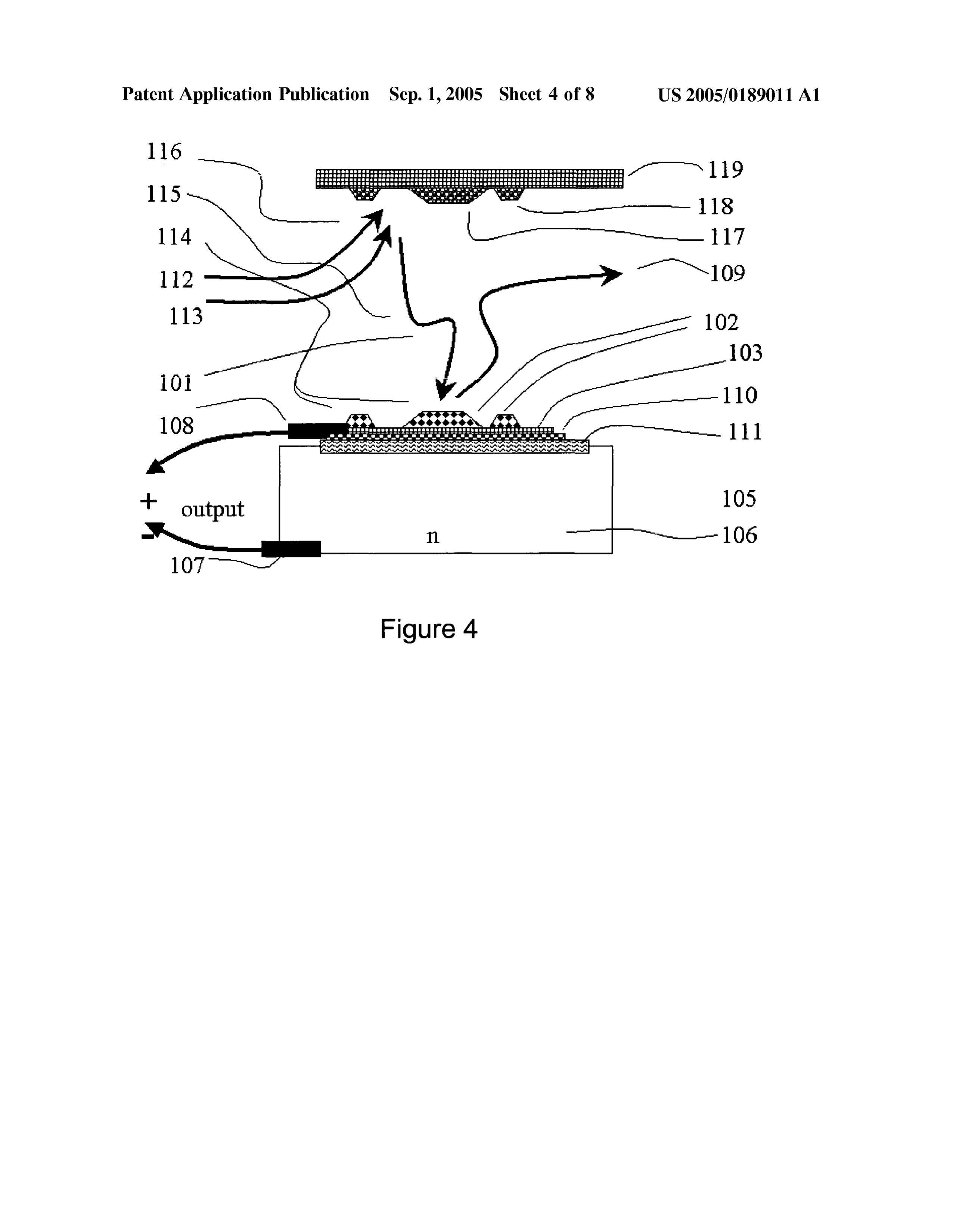
Page 17
US 2005/0189011 A1 Sep. 1, 2005
0.093 Highly doping the semiconductor 104, including diffusion length of the minority carriers transporting the the limit of high doping called degenerative doping, and energy. This kind of mean free path is often referred to as the selecting the electrode material 110 or 111 from the ones diffusion length. Over distances longer than the diffusion known to be compatible with forming an electrical contact length the carriers eventually recombine and generate heat. to a Semiconductor reduces the Schottky barrier between an Such diffusion lengths are typically of order 200 nm or electrode and a semiconductor. The electrode material 111 OC.
may also be another Semiconductor, which is a method 0100. The diode 104, 105, 106, in one aspect, may be routinely used in the State of the art of Semiconductor device Similar to a photovoltaic diode, but different in a key, fabrication. The result is that the conducting surface Fermi non-obvious way. The known photovoltaic diode must be level and the Fermi level of the p-type semiconductor formed with a region near the junction large enough to Valence band (the top edge of the lower band) are equal. The collect the light passing through it. This is typically much hot carrier energy is measured relative to that of the con larger than a few hundred nanometers. To increase the light ducting surface Fermi level. The result is that some hot collection distance, the Semiconductor junction must contain carriers approach the Semiconductor with an energy above at least one relatively lower doped region. This constraint that of the conducting surface Fermi level and therefore with forces the doping of either the n or p region of the photo approximately the same energy above the Fermi level of the voltaic diode to be much less than what is considered to be p-type Semiconductor. heavy doping or degenerate doping. This lower doping level 0094. The hot carrier then tries to enter the semiconduc reduces the resistance area product of the diode and hence tor 104 with an excess energy above that of the conducting reduces its efficiency.
Surface 102,103 and/or 110 and semiconductor 104 valence band. By this design, there are practically no energy levels 0101 Unlike the known photovoltaic diode, the diode inside the band gap of the Semiconductor for an electron to 104,105,106 does not need to collect such photons and does excite. The only levels available to the hot electron in the not need a large photon collection region. Therefore, the Semiconductor 104 are in the upper band, the conduction diode 104,105,106 in the apparatus does not need one or the band. other polarity region of the Semiconductor to be low doped. 0.095. In one aspect, the location of this upper band is The diode 104, 105, 106 may, therefore, use the highly doped or degeneratively doped Semiconductor as a free chosen to be slightly less than the dominant energy of the parameter of engineering design. This doping maximizes the electrons, So the electron can readily enter the Semiconduc resistance area product and, therefore, maximizes the diode tor 104. This is achieved by fabricating the band gap of the efficiency. Therefore, the diode 104,105,106 may have both semiconductor 104 to be less than a chosen energy of this in 106 and p 104 regions that are highly or degeneratively hot electron Spectrum, or by choosing a Semiconductor with doped. Unlike in a photovoltaic diode, high doping increases the desired band gap. This means that a desired fraction of the energy collection efficiency of the diode. High doping the hot electrons enter the p-type semiconductor 104 in its also increases the electric field tending to Sweep the injected conduction band. This energizes the conduction band of the minority carrier across the junction 105. p-type semiconductor 104. The electron is thus converted into a minority carrier instead of a ballistic carrier. The 0102) Accordingly, the semiconductor 104 may be minority carrier typically has a lifetime orders of magnitude degeneratively doped to a shallow depth, for example, 0.1 to longer than that of the ballistic carrier. 0.5 microns (100 to 500 nanometers). Highly doped and 0096. In another aspect, the semiconductor is chosen to degenerative doped Semiconductors may be used to mini be n-type when the hot carrier is a hole. The complimentary mize the distance from the conductor 110, 111 to the Surface proceSS as described with reference to p-type Semiconductor of the diode 104, where the hot carriers are generated, to the is performed, producing the Same result, i.e., the Short-lived p-n junction 105, where the forward bias is developed. Thus carrier is converted into a longer-lived carrier. Advanta the high doping and Small p-n junction dimensions become geously, Semiconductor materials with both indirect and a useful method. The high doping also permits use of direct band gaps are available with energies from the lowest relatively thin Semiconductors, Such as Semiconductors leSS practical, of order 0.05 eV to higher than the bond energies than 1 micron thick. It also permits convenient doping of most reactants, well in excess of 3 eV. practices.
0097. The lifetime of a minority carrier in a semiconduc 0103) The method and apparatus provided produces prac tor is typically at least 100 times longer than that of a tically useful efficiencies (in excess of 20%) and may be ballistic carrier. This longer lifetime gives the hot, minority achieved with energized molecule power densities as low as carrier a chance to migrate, diffuse or be attracted by the of order 10 watts per square centimeter. The efficiency of the Semiconductor internal field to a region in the Semiconductor diode sharply increases with power, So that using more than of opposite type, namely an n-type Semiconductor. The p-n 10 watts per Square centimeter may result in much higher junction creates a strong electric field acroSS it and attracts efficiency than at 10 watts, e.g. a nonlinear advantage. minority carriers approaching it. 0104 FIG. 2 shows a cross section of the energy con 0098. At the semiconductor junction, the minority carrier verter portion of an apparatus in one embodiment of the in the Semiconductor finds exactly the same situation as it invention. In this embodiment, gas phase energized mol would find in a photovoltaic diode. AS in a photovoltaic ecules 101 create hot energetic electrons which travel into a diode, the electric field of the p-n junction Sweeps the hot p-n junction semiconductor diode 104,105 and 106, forward carrier acroSS the junction, forward biases the diode and biasing it and generating electricity. AS shown, energized generates a useful electrical potential. molecules 101 flow on to the conducting surface 102 and 0099. In one aspect, the p-type semiconductor 104 diode 103. De-energized molecules 109, also referred to as exhaust layer thickness is chosen to be Smaller than the energy products, leave the conducting surface 102 and 103 region.
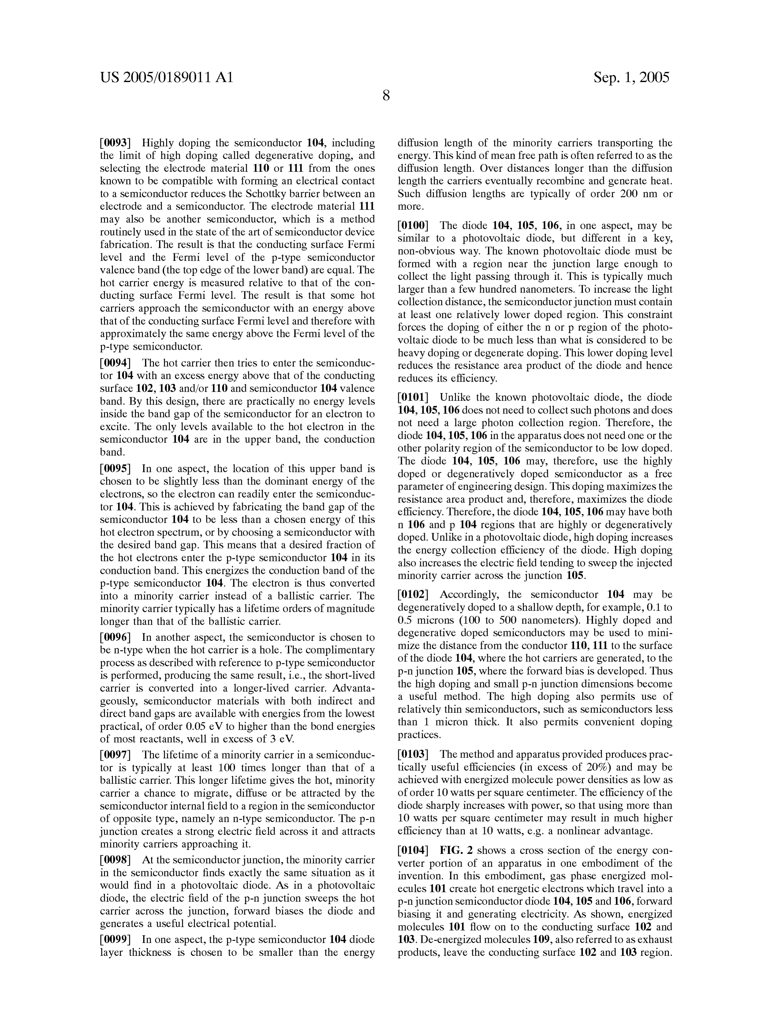
Page 18
US 2005/0189011 A1 Sep. 1, 2005
Hot electrons are produced as a result of the gas-Surface energized molecules create hot energetic electrons which interaction and forward bias the Semiconductor diode travel into a Schottky junction Semiconductor diode, for formed by p type semiconductor 104, p-n junction 105 and ward biasing it and generating electricity. Gas phase ener in type semiconductor 106. gized molecules 101 flow on to the conducting Surface 102 0105 The conducting surface includes optional catalyst and/or 103. De-energized molecules 109, also referred to as 102, conducting material 103, optional interface conducting exhaust products, leave the conducting Surface region. Hot electrode 110, and optional interface 111, Such as a p type electrons are produced as a result of the interaction. Hot semiconductor. The conducting material 103 forms a Sub electrons with energy above the Schottky barrier travel into strate for the an interaction with energized molecules 101. the semiconductor diode 110, 111 and 104 and forward bias Optionally, the optional catalyst structures 102 may be it. The diode 110, 111 and 104 is formed by the junction of formed on this conducting material 103. the conducting Surface 110 and the n type Semiconductors
0106 Optional interface conducting electrode 110 and 0111. In another aspect, the conducting Surface may optional interface p type Semiconductor 111 are shown to include optional catalyst 102, conducting material 103, illustrate that material constraints may force the need for optional interface conducting electrode 110, and optional different types of materials. For example, one type of interface in type Semiconductor 111. Optional interface con conducting material 103 may be needed for optimal inter ducting electrode 110 and optional interface in type Semi action with energized molecules 101. Another type of con conductor 111 are shown to illustrate that material con ducting material 110 may be needed to form an ohmic or Straints may force the need for one type of conducting almost ohmic connection to a Semiconductor 111. This material 103 facing energized molecules 101 and for another ohmic connection may be needed for the ohmic connection type of conducting material 110 facing SemiconductorS 111 to the diode semiconductor 104. When materials are com patible, material 102, 103 and 110 may be formed from the and 104. The conducting material 103 forms a substrate for the preferred interaction with energized molecules. The
Same material, Such as a conductor. The diode material 111 optional catalyst Structures may be also formed on the and 104 may be also be the same. conducting material 103. The conducting material 110, 0107 For example, when the semiconductor 111 is very which may be of another type, is used to form Schottky heavily doped, also referred to as degeneratively doped, junction to a semiconductor 111. Semiconductor 111 and catalyst 102 or metal 103 or 110 may form an ohmic junction semiconductor 104 may in some designs be the same. When or an almost ohmic junction to the Semiconductor 111. In materials are compatible, the materials for catalyst 102, this case, a catalyst 102 or a conductor 103 may act as the substrate 103 and electrode 110 may be formed from the substrate 110 to connect the conducting surface to the Same material Such as a conductor. For example, a catalyst Semiconductor diode. or metal may form a Schottky junction to the Semiconductor. 0108. The hot electrons created on the conducting surface In this embodiment, a catalyst 102 or a conductor 103 or 110 102 and 103 are ballistic majority carriers in the conductors. may act as the electrode 110 to connect the conducting Surface to the Semiconductor diode.
Those electrons with energy Sufficient to enter the Semicon ductor conduction band travel into the p-type Semiconductor 0112 The hot electrons created on the conducting surface 104 where the electrons are converted into minority carriers. 102, 103 and 110 are ballistic majority carriers in the Charge balance occurs by the transfer of a low energy hole conductors and travel into the n-type Semiconductor 111 and to the p-type Semiconductor 104 from the conducting Sur 104 where the electrons are also majority carriers. In the face 102 and 103. The minority carriers travel to the p-n process, the electrons loose energy to heat approximately junction 105 of the diode both by diffusion and by reason of equal to the difference between their initial energy above the the internal electric field of the junction 105. The internal Schottky barrier and the Fermi level of the n type semicon electric field causes the carriers to become majority carriers ductor.
in the n-type Semiconductor 106 of the diode, causing the 0113 Collisions with the lattice and electrons in the diode to become forward biased. The forward bias devel Semiconductor degrade the excess energy to a value Sub oped acroSS the diode generates electricity. This electricity is stantially less than the barrier. The result of this energy loss extracted as a forward current between the positive electrode is to diminish the number of electrons that travel in the 108 and the negative electrode 107. reverse direction. This permits a forward bias on the diode 0109 Referring to FIG. 2, in another aspect, the reaction to develop.
region near 101, 109 and near 102, 103 may include a 0114 Charge balance occurs by the transfer of a hole surface of the collection region 102, 103. Catalysts included from the conducting surface 110. The electrons cause the in 102 and/or reaction Stimulation mechanisms included in diode 110, 111 and 104 to become forward biased. Electric 102 co-located with the conducting surface 102, 103 are ity is generated by reason of the forward bias developed used to cause fuels and oxidizers 101 to react and for across the diode 110, 111 and 104 and is extracted as a products 109 including energized molecules 109 to be forward current between the positive electrode 108 and the formed on the conducting surface 102, 103, in the volume negative electrode 107.
region above the surface 102, 103 and near 109, or in the 0115 The substrate 110 may be a conductor chosen to immediate vicinity of that surface 102, 103. The term “near” form a Schottky barrier at the metal-Semiconductor junction. means within Several diffusion dimensions of energetically The substrate 110 therefore may also form the electrical excited products in the product stream 109, as explained in connection to the diode, also referred to as the diode this disclosure. electrode.
0110 FIG. 3 shows a cross section of an energy con 0116 FIG. 4 shows a cross section of an apparatus that verter portion of the apparatus for the case where the is functionally similar to the device described with reference
Page 19
US 2005/0189011 A1 Sep. 1, 2005
to FIG. 1. The difference is that the semiconductor diode ductor 106 which diffuse to other regions 131 of the semi shown in FIG. 4 is a Schottky junction instead of the p-n conductor, including along the junction 130. There, the hot junction of FIG. 1. carriers may be used for other purposes. In FIG. 5, the elements of the collecting region, reactants 101, exhausts 0117. In both devices of FIGS. 1 and 4, it may be readily 109, optional catalyst 102, conducting Surface 103, interface concluded and observed that the physical location of the conductor 110, interface Semiconductor 111, p-type Semi reaction region 116 may be any one of 1) identical to the conductor 104, junction 105 and n-type semiconductor 106 collection region 114; 2) adjacent to the collection region may be functionally similar to those of FIG. 2. 114 on the same substrate 102, 103 and 110; 3) near the collection region 114 on nano-structures or micro-structures 0123 The semiconductor region 106 shown as n-type near the collection region 114; 4) entirely separate from the may instead be p-type with lower doping than the p-type collection region, or 5) comprising Several different kinds of region 104, or the region 106 may be intrinsic (undoped). reaction Stimulator in different locations. Application of electrical Signals between the region 106 and the p-type region 104 may be used to control the movement 0118. In another aspect, the devices shown in FIGS. 1 and Storage of the carriers.
and 4 illustrate how the physical Separation of reaction region and collection region may facilitate thermal consid 0.124. In one aspect, Semiconductor Structures may be erations. That is, the reaction region may be kept at a designed to Store charge carriers resulting from the hot temperature much higher than the collection region by electrons. Such Semiconductors may collect hot electrons in reason of the physical Separations. one region and permit the resulting longer lived carriers to 0119) The reaction regions 116 shown in FIGS. 1 and 4 diffuse to other regions. The invention may distribute the may be a thin cylinder, for example, shaped like a wire, long lived carrier to other locations on the reaction Surface. Surrounded coaxially by a collection region shaped as a The transported carriers may then leave the Semiconductor, cylinder or box of much larger dimension. The reaction convert back into a ballistic carrier in a conducting Surface region 116 may be a planar Surface of the same dimension or reaction Surface, and perform useful work. Such work as the collection region, for example, as opposite sides of a includes Stimulating reactions and energizing nano-me box structure or opposite Sides or walls of a channel Struc chanical devices or molecules. Examples of Such nano ture. The reaction region 116 may be a set of wire-like mechanical devices include a nano-propeller, a C60 transis regions Separated from and above a sheet-like collection tor, and the biological material kinesin. region 114 surface. The collection region 114 may be 0.125 The carriers in other regions may cause a popula constructed as a plateau or post, Surrounded by wire-like tion inversion of electrons and holes in the Semiconductor, reaction region devices, point-like reaction regions. These or may cause a transport of the carriers to another Surface for configurations are only shown as examples of ways to injection into that Surface, or may cause a transport of the Separate reaction and collection regions. The configurations carriers to a region where they perform Some other useful of FIGS. 1 and 4 show the generic concept of separated purpose.
regions.
0.126 Examples of other purposes include injecting car 0120 Referring to FIG. 1 and FIG.4, in another embodi riers into a Semiconductor to control currents Such as in a ment the reaction region 115, 116 may be designed to transistor, re-injection of carriers from a Surface of the operate at an elevated temperature relative to the collection Semiconductor 131 into adsorbates on its Surface or Surfaces region 114. The reaction region 115, 116 may include connected to it to cause chemical reactions or to energize the reaction stimulators 117, 118, 119 such as electrical, optical adsorbates to become more reactive or to become energeti or chemical injection Stimulators, which may require ther cally excited; causing chemical reactions, controlling mal isolation, electrical isolation, optical guides, and chemi chemical reactions, Stimulating reactions, energizing Surface cal injectors. The reaction region 115, 116 may include heat adsorbates into excited States, energizing Surface plasmons, SinkS, not shown in either figure, Separate from that of the injection of carriers into piezo-electric or electroStrictive collection region 114. Heat may also be removed by con elements to cause conversion to mechanical motion; causing vective action of the gas flow 109 through the reaction a population inversion So as to cause optical emission; region 115, 116. injection into quantum well Structures to cause electromag 0121 The reaction region 116 includes stimulators or netic emissions, energizing Semiconductor circuits, and/or conversion to other forms including phonons.
catalysts. These may include a structure 119, electrical
Stimulators, optical Stimulators, catalysts shown generally as 0127 FIG. 6 shows a cross section of an apparatus 117, hot wires or structures shown generally as 118, and functionally equivalent to that of the device described with injected chemical StimulatorS Such as autocatalysts and free reference to FIG. 5. In the device shown in FIG. 6, the use radical generators or reaction Stimulators. Examples of addi of the carriers in the semiconductor p-n junction 105 is an tive autocatalysts and free radical generators include use of inverted population. In this mode, the energy 111 is extracted additives Such as hydrogen peroxide and methyl alcohol. from the diode in a fashion similar to that of a laser diode or a light emitting diode, where elements 112 represent optical 0.122 FIG. 5 shows a cross section of a device that stores elements. The operations of laser diode and light emitting excitations created by excited molecules. The device may be diode is generally known to those skilled in the art, and similar to one described with reference to FIG. 2. In the therefore, will not be further explained herein.
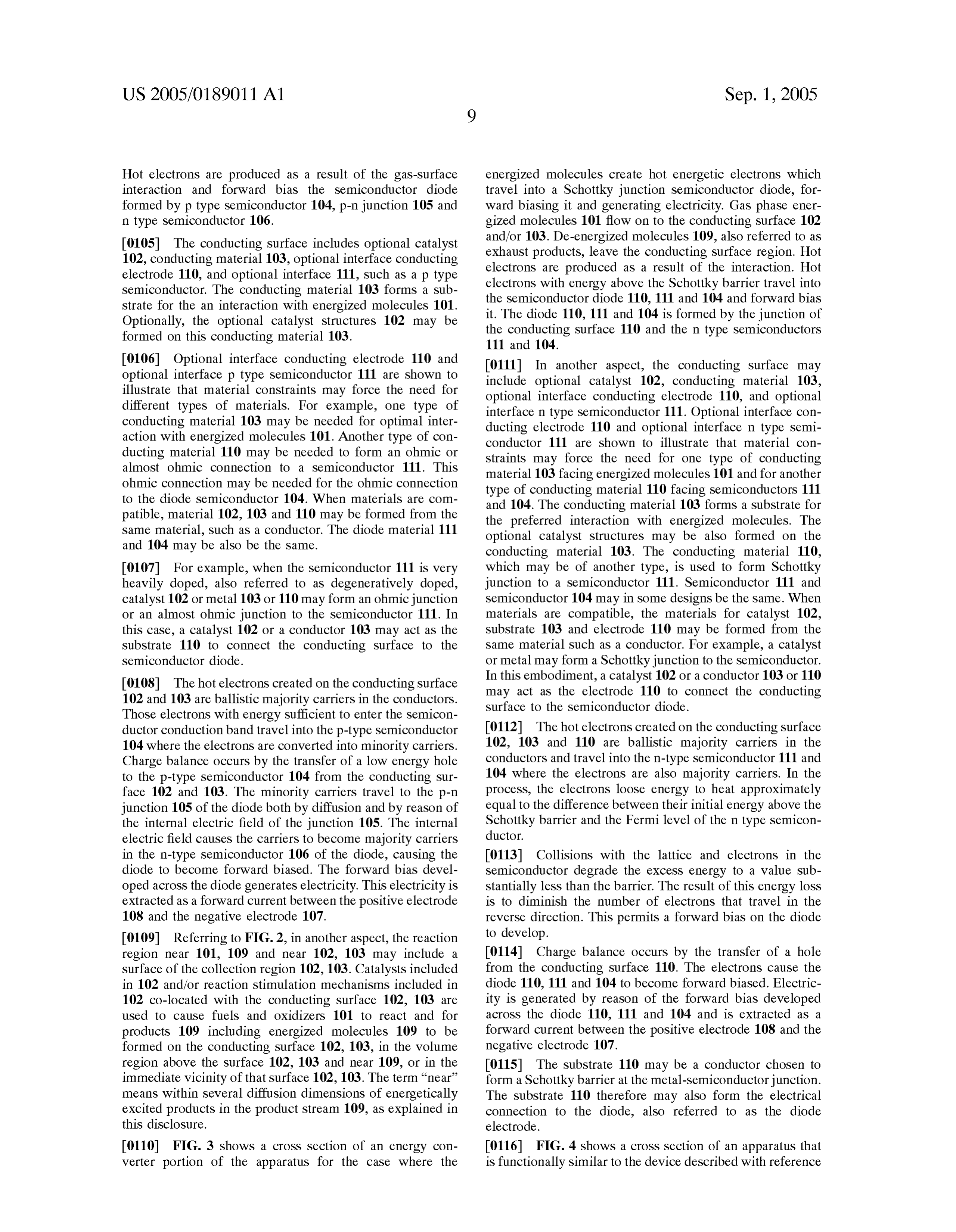
device shown in FIG. 5, the hot electrons may be used in other ways than generating electricity. The hot electrons 0128 FIG. 7 illustrates the apparatus with separate reac originating from energized molecules form electrons in the tion and collection regions. The reaction region 713, which p type Semiconductor 104 and holes in the n type Semicon includes catalysts 703 and/or reaction stimulators 701, 702,
Page 20
US 2005/0189011 A1 Sep. 1, 2005
may be located at one part of a substrate 710 and the 0.134. Using a Schottky junction as an energy converter collection region 714 including the conducting surface 704 may provide for Simplicity in the device. Semiconductors and its associated Semiconductor converter elements with band gaps in the range of order 1 volt, Such as Silicon (including conducting surface 704, interface conductor 705, may be used. In one aspect, higher band gap Semiconductors electrode 706, p-type semiconductor 707, juntion 708, may be used and, therefore, permit the apparatus to be n-type semiconductor 709, substrate 710) on another part of operated at a temperature above room temperature, e.g. the Substrate. above 100 Celsius. Commercially available high tempera 0129. As shown in FIG. 7 the reaction region 713 may be ture SemiconductorS Such as GaN and SiC are examples of designed relatively Smaller than the collection region 714. Such higher band gap materials. This expands the range of The reaction region 713 may also be arranged among or metals and Semiconductors that may be used and results in partly enclosed by relatively larger collection regions 714. increased extractable power per area. The catalyst 703 of the reaction region 713 also may be 0135) In one aspect, energized molecules may be used to Separated from the collection region 714, which partly generate the carriers instead of an applied Voltage for encloses the reaction region 713. powering an external device. Energized molecules may 0130 Referring to FIG. 7, fuel channels 715 may be therefore be used to power devices that would otherwise be formed separate from air or oxidizer flow 716. This sepa powered by a Source of electricity. For example, chemical ration can take on many forms. For example, a collection reactions may also be used to power chips Sets. Using region 714 may be formed with holes 712 that penetrate to chemical reactions to power chips Sets permits the construc an underlying source of fluid fuel 715. Fuel molecules 113 tion of Volume, three dimensional computing Systems, would thus dominate the adsorbed specie on the catalyst 703 where the energy Source to power them is a flow fuel oxidizer mixture instead of electrical connections. This or collection 714 regions. The catalyst-fuel assembly may be permits Systems without physical interconnects and without part of the collection Surface 704 or it may be part of the any structural interconnects, for example, as in pebble bed reaction Surface 703, or both. reactor Systems. MicroStacks of electrical energy Sources 0131 The fuel and/or the heat of vaporization of a fuel may be energized by the fuel-oxidizer mixtures, where Such may be used to cool the Semiconductor energy converter, microStacks are part of the physically isolated "pebbles.” which may include, for example, conducting Surface 704, This in turn permits Self assembled Volume Systems, and interface conductor 705, electrode 706, p-type semiconduc greatly lowers their cost and increases their performance. tor 707, junction 708, n-type semiconductor 709, Substrate 0.136. In another aspect, a quantum well is used and 710. This is a novel way both to cool the semiconductor and energized as the energy converter. An energy converter of to enhance the re-use of hot carriers that do not become converted into electricity. For example, referring to FIG. 7, the apparatus transforms a short-lived carrier into a longer a fuel 113 covering a catalyst or conduction surface 704 may lived carrier So that the resulting carrier may be further used. absorb hot electrons that do not enter the energy converter A quantum well Substrate including a tunneling barrier, a semiconductor 708. Upon absorption, the fuel may then metal or Semiconductor and another tunneling barrier may dissociate into active radicals and become part of a chemical be used to form the energy converter. This energy converter reaction. The fuel or its dissociated products may desorb, may be also formed in direct contact with the substrate with or without help of hot electrons, and mix with radicals Semiconductor. Another way the energy may be extracted in the reaction region 713. Fuel may also simply evaporate may be through generation of a potential. Yet another way from regions 712 which are physically connected to the may be to power nanodevices directly connected to the semiconductors 708, 709 and pass into the reaction region invention. According to the State of the art, external electric 713, cooling the semiconductors 708, 709. The high con currents have been used to energize quantum wells and dots centration of vaporized fuel 113 can therefore bias the formed into near ideal 4 level lasers. In the apparatus fuel/oxidizer mixture in favor of an optimum mixture. provided, the same kinds of Wells and dots may be energized directly from the energy of injected carriers.
0132) Referring to FIG. 8, thermal barriers 810 may be 0.137 Quantum wells also offer the possibility of creating formed between the reaction 811 and collection 812 regions resonances to capture the energized molecule excitations. So that the reaction region 811 may operate at a higher The resonance levels formed by the quantum well may be temperature than the collection region 812. Such barriers tailored to match Selected multi-quantum transitions in the may include pillars 810, vacuum or channels with reduced chemically excited products. Such a match provides a way amounts of physical material. Heat Sources may be con to transfer energy from the excited products into the longer nected to the reaction region 811 and heat Sinks to the lived excitation of the quantum well. The method provided, collection region 812 to keep the regions within their desired for example, may extract the energy from the quantum well operating ranges. The reaction region 811 may be formed by Stimulated emission of radiation. with elevated Structures Such as posts, plateaus and/or pillars 810. Structures may be designed to be thermally insulating. 0.138. The current state of the art associated with semi 0.133 Referring to FIG. 8, electrically insulating barriers conductor or metal quantum well Structures permits layers 810 may be formed between the two regions 811, 812 so that whose dimensions are, conveniently, less than or of the same electrical Stimulation Signals may be routed to the reaction order of magnitude as the energy diffusion length of the region without interfering with the collection region. Other ballistic carriers involved, facilitating and enabling fabrica tion.
barriers and structures may be placed between the regions, for example to isolate or filter radiation, or to filter chemical 0.139. In one aspect, the conducting surface may include by products, or to isolate molecules with various properties several materials. The surface is formed sufficiently thin, for Such a translational, rotational or compositional properties. example, with thickneSS less than 10 times the energy
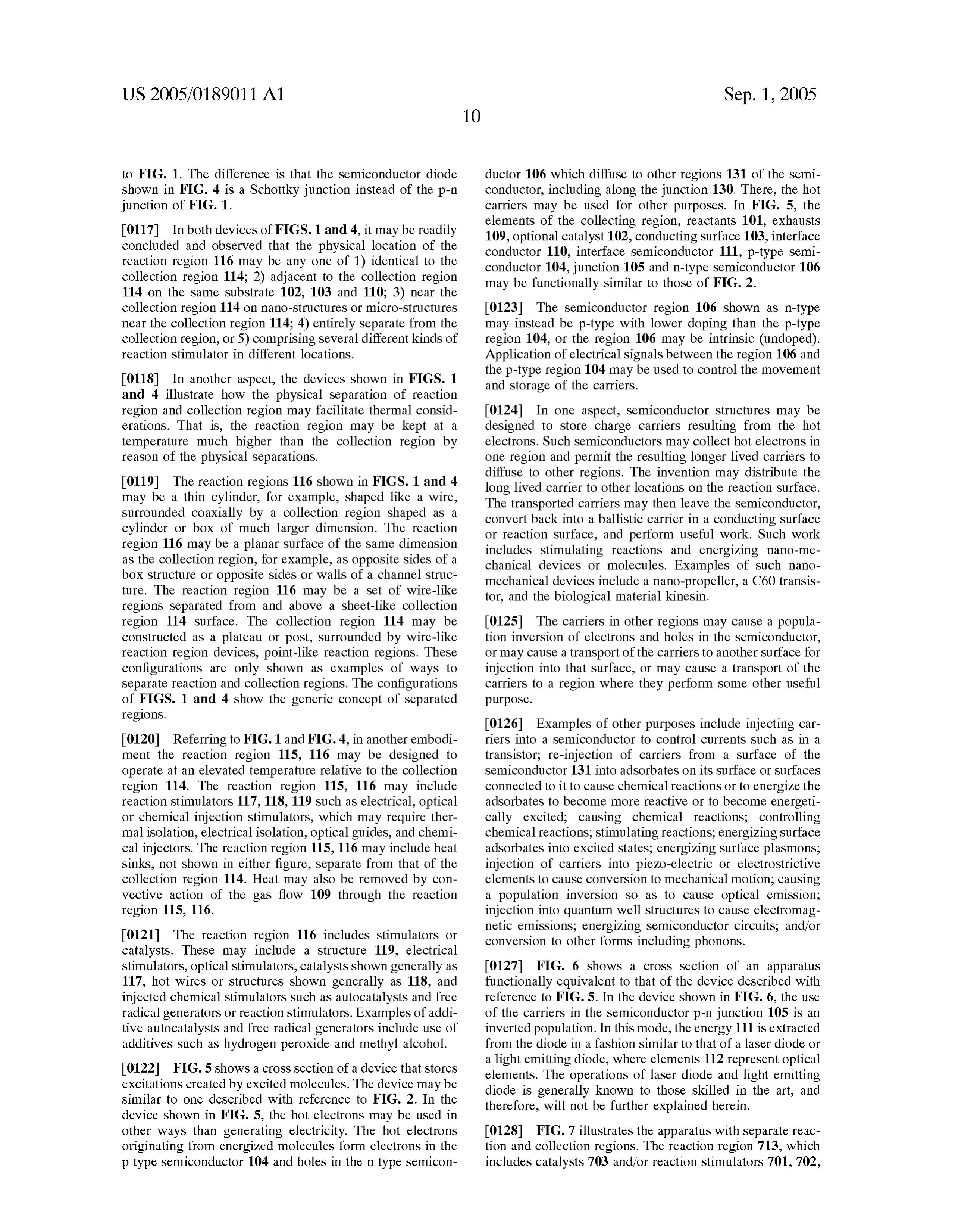
Page 21
US 2005/0189011 A1 Sep. 1, 2005
diffusion length for hot electrons, on a Semiconductor Struc 37. (canceled) ture Such that hot electrons may enter the Semiconductor 38. (canceled) before loosing a Substantial fraction, for example, no more 39. The method of claim 33, wherein the semiconductor than 90%, of their energy. diode comprises a pnjunction diode; and the forming a thin 0140. The conducting surface and its underlying semi electrically conducting Surface comprises forming a thin conductor may include catalysts and other reaction Stimu electrically conducting Surface on a highly doped or degen lation Systems to cause chemical reactions of the energized eratively doped p-type Semiconductor and a junction molecules or to cause energy transferS either from or to the between the thin electrically conducting Surface and the energized molecules. That is, the conducting Surface may highly doped or degeneratively doped p-type Semiconductor also be part of a reaction-Stimulating Surface energized by forms an ohmic or almost ohmic contact; and the tailoring the application of energy, Such as electricity. one or more properties comprises tailoring bandgap of the pnjunction diode to create a barrier profile.
0.141. The conducting surface and its underlying semi 40. The method of claim 39, wherein the tailoring band conductor may include catalysts and other reaction Stimu gap comprises varying composition of the one or more lation Systems. These may be used to prevent adsorbates, Semiconductor elements as a function of distance from the Such as fuels, oxidizer, exhausts, reaction byproducts, or junction between the thin electrically conducting Surface and other materials, from clogging, accumulating or interfering the highly doped or degeneratively doped p-type Semicon with the operation of the conducting Surface, as is known to ductor.
happen when non-conductors form or collect on the con 41. The method of claim 40, wherein the vaying com ducting Surface. These catalysts and other reaction Stimula prises periodically varying the bandgap for forming quan tion Systems may also accelerate the reactions and may tum wells with energy levels chosen to match one or more cause preferred reactions to occur. energy levels of the products of the chemical reactions. 0142. While the invention has been particularly shown 42. (canceled) and described with respect to an embodiment thereof, it will 43. The method of claim 40, wherein the semiconductor be understood by those skilled in the art that the foregoing elements comprise germanium and Silicon and composition and other changes in form and details may be made therein of the silicon is varied.
without departing from the Spirit and Scope of the invention. 44. The method of claim 32, further comprising: 1-31. (canceled) cooling the one or more Semiconductor elements by 32. A method of producing electrical energy, comprising: convective flow, heat of vaporization, or conduction, or forming a thin electrically conducting Surface on one or combination thereof.
more Semiconductor elements, the thin electrically con 45. The method of claim 44, wherein the forming a thin ducting Surface and the one or more Semiconductor electrically conducting Surface comprises forming a thin elements forming a Semiconductor diode, electrically conducting Surface on one or more Semiconduc forming a region for chemical reactions, the region tor elements, the thin electrically conducting Surface and the including at least the thin electrically conducting Sur one or more Semiconductor elements forming at least one of face;
a Semiconductor diode and a capacitor or combination thereof, wherein the electrons cause a useful potential acroSS conveying reactants into the region; the Semiconductor diode or the capacitor. initiating one or more chemical reactions in the region, the 46. The method of claim 45, wherein the useful potential chemical reactions producing one or more highly vibra acroSS the Semiconductor diode comprises a forward bias acroSS the Semiconductor diode.
tionally excited reaction products, and 47. The method of claim 45, wherein the useful potential removing exhaust and one or more products of the chemi acroSS the capacitor comprises a voltage across the capacitor. cal reactions from the region by gas convection, 48. The method of claim 44, wherein the heat of vapor wherein the one or more highly vibrationally excited ization comprises heat of vaporization of one or more reaction products transfer reaction product energy to reactants, liquids, fuels, or additives, or combination thereof. electrons in the thin electrically conducting Surface, 49. The method of claim 44, wherein the convective flow which electrons become energetic, travel into the one or comprises using a flow of air, the reactants, the products of more Semiconductor elements and produce electrical chemical reactions, fuels, liquids, or additives, or combina energy. tion thereof.
33. (canceled) 50. The method of claim 44, wherein the convective flow 34. The method of claim 32, wherein the semiconductor comprises using a heat pipe that uses heat of vaporization to diode comprises at least a Schottky diode; and remove heat from the Semiconductor diode or the region or combination thereof to cool the one or more Semiconductor the method further includes tailoring barrier width of the elements.
Schottky diode for enhancing tunneling of the electrons from the thin electrically conducting Surface to the one 51. (canceled) or more Semiconductor elements. 52. The method of claim 44, further comprising integrat 35. The method of claim 34, wherein the tailoring barrier ing the Semiconductor diode as a part of a System that width comprises choosing a Semiconductor doping between performs the conveying Step.
high limit of degenerative doping and lower limit of light 53. The method of claim 44, further comprising integrat doping. ing the Semiconductor diode as a part of a System that 36. (canceled) performs the removing Step.
Page 22
US 2005/0189011 A1 Sep. 1, 2005
54. The method of claim 44, further comprising integrat flowing gaseous reactants into the region for chemical ing the Semiconductor diode as a part of a System that reactions, and performs the conveying Step and the removing Step. providing an exhaust path from the region. 55. (canceled) 71. The method of claim 32, wherein the removing 56. The method of claim 44, wherein the conveying exhaust and reacted products comprises: comprises conveying reactants into the region by pulsed removing spent reactants from the thin electrically con delivery Such that one or more reaction products are allowed ducting Surface.
to desorb and conveyed out of the region during the period 72. The method of claim 71, wherein the removing spent between the pulsed delivery. reactants comprises using a catalyst as part of the thin 57. The method of claim 44, wherein the initiating com electrically conducting Surface.
prises Stimulating one or more reactions in the region by 73. The method of claim 71, wherein the removing spent using a catalyst, injecting a stimulant, injecting an autocata reactants comprises applying periodic Stimulation to the thin lyst, injecting hot carrier, using electrical Stimulant, using electrically conducting Surface. optical Stimulant, or using a plurality of reactants, or com 74. The method of claim 73, wherein the stimulation bination thereof. comprises heat, electrical, optical, mechanical, ultrasonic, or 58. The method of claim 32, further comprising: hot carrier injection Stimulation, or combination thereof. 75. The method of claim 32, wherein the conveying preparing the reactants prior to producing the one or more reactants comprises conveying reactants that produce highly highly vibrationally excited reaction products. Vibrationally excited reaction products. 76. The method of claim 75, wherein the reactants com 59. The method of claim 58, wherein the preparing prises one or more of monopropellants, or unstable energetic comprises reforming, desorbing, adsorbing, reacting, modi Specie, or combination thereof. fying one or more chemical properties of the reactants, 77. The method of claim 76, wherein the reactants com condensing, or vaporizing, or combination thereof, by using prise monomethylhydrazine or high explosives, or combi one or more catalysts, Separated catalysts, reaction Stimula nation thereof.
tors, Separated regions, or multiple regions, or combination 78. (canceled) thereof. 79. The method of claim 32, wherein the thin electrically 60. The method of claim 58, wherein the preparing conducting Surface is formed as having monolayer features. comprises using a catalyst and a reactant to provide energy 80. (canceled) for vaporization. 81. The method of claim 32, wherein the thin electrically 61. The method of claim 58, wherein the preparing is conducting Surface is formed from platinum, palladium, performed intermittently in pulses or periodically. gold, rhodium, or ruthenium, or combination thereof. 82. The method of claim 32, wherein the thin electrically 62. The method of claim 32, further comprising tailoring conducting Surface is formed on an intermediate Surface. spent or unused reaction products for conveyance to an 83. The method of claim 82, wherein the intermediate exhaust. Surface comprises metal or oxide or combination thereof. 63. The method of claim 62, wherein the tailoring spent 84. The method of claim 32, wherein the one or more or unused reaction products comprises desorbing, adsorbing, Semiconductor elements comprise photovoltaic energy con reacting, modifying chemical properties of the spent or verter devices, metal-insulator- metal devices, metal-oxide unused reaction products, condensing, or vaporizing, or metal devices, or quantum wells, or combination thereof. combination thereof, by using a catalyst, Separated catalysts, 85. The method of claim 32, wherein at least one of the reaction Stimulator, Separated regions, or multiple regions, one or more Semiconductor elements are chosen from those or combination thereof. with band gap greater than approximately 1.0 eV. 64. The method of claim 62, wherein the tailoring is 86. The method of claim 32, wherein the one or more performed intermittently in pulses or periodically. Semiconductor elements comprise a catalyst oxide, a high 65. The method of claim 62, wherein the catalyst com temperature wide band gap Semiconductor, or combination thereof.
prises aluminum.
66. The method of claim 62, wherein the reaction stimu 87. The method of claim 86, wherein the catalyst oxide lator comprises periodic pulses of H2O. comprises TiO2.
88. The method of claim 86, wherein the high temperature 67. The method of claim 62, wherein reaction stimulator wide band gap Semiconductor comprises SiC, GaN, GaP, comprises reactants that burn the Spent or unused reaction diamond, or ZnO, or combination thereof. products. 89. The method of claim 86, wherein the one or more 68. The method of claim 32, further comprising using a Semiconductor elements comprise Silicon or GaAS or com catalyst with a low affinity for reacted products, the catalyst bination thereof.
being used to prepare for and enhance the producing of the 90. (canceled) one or more highly vibrationally excited reaction products 91. (canceled) and to tailor the reacted products for the removing. 92. The method of claim 32, wherein at least one of the 69. The method of claim 68, wherein the catalyst with a Semiconductor elements is in contact with the thin electri low affinity for reacted products comprises platinum, palla cally conducting Surface and has a bandgap greater than dium, or gold, or combination thereof. bandgaps of rest of the Semiconductor elements. 70. The method of claim 32, wherein the removing exhaust and reacted products comprises:
Provenance
- Collection
- Patents citing this work
- Original assignee
- Neokismet LLC
- Pages
- 22
- Method
- pdftotext (the PDF's own text layer) + pdftoppm 300dpi page scans
- Patent office record
- patents.google.com →
- Source
- Google Patents citing-documents table
- Inventors
- Anthony Zuppero; Jawahar Gidwani; Neokismet LLC
- Published
- 2005-09-01
- Transcribed from
- patentimages.storage.googleapis.com →