patent · US20020017827A1
Pulsed electron jump generator
14 February 2002
Page 1 — bibliographic record
(19) United States (12) Patent Application Publication (10) Pub. No.: US 2002/0017827 A1
Zupper0 et al. (43) Pub. Date: Feb. 14, 2002 (54) PULSED ELECTRONJUMP GENERATOR Publication Classification
(76) Inventors: Anthony C. Zuppero, Pollock Pines, (51) Int. Cl. ................................................... HO2N 1/00 CA (US); Jawahar M. Gidwani, San (52) U.S. Cl. .............................................................. 310,300 Francisco, CA (US)
Correspondence Address: (57) ABSTRACT
BAKER & MCKENZE
805 THIRDAVENUE
NEW YORK, NY 10022 (US) A device and method for Stimulating pulsed chemical reac tions in a Small Volume of gaseous reactants. An emitter (21) Appl. No.: 09/682,363 Stimulates the reactions of a fuel Oxidizer mixture and a (22) Filed: Aug. 24, 2001 collector converts the vibrational energy of the resulting products into useful energy. The device may also include a
Related U.S. Application Data reaction region, a collector, and reactants Such as fuel and oxidizer. In one embodiment, air including exhausts is made (60) Continuation-in-part of application No. 09/589,669, to flow into and out of the reaction region, and fuel is made filed on Jun. 7, 2000, which is a division of applica to flow into the reaction region. The device may be config tion No. 09/304,979, filed on May 4, 1999, now Pat. ured in Several geometries, including but not limited to, a No. 6,114,620. V-channel, a box and a plane.
exhaust flow
Page 2
Drawing sheet — no readable text.
Page 3
Drawing sheet — no readable text.
Page 4
Drawing sheet — no readable text.
Page 5
Drawing sheet — no readable text.
Page 6
Drawing sheet — no readable text.
Page 7
Drawing sheet — no readable text.
Page 8
Drawing sheet — no readable text.
Page 9
Drawing sheet — no readable text.
Page 10
Drawing sheet — no readable text.
Page 11
US 2002/0017827 A1 Feb. 14, 2002
PULSED ELECTRONJUMP GENERATOR confined to a Small volume, e.g., when dimensions of the confining Volume are the order of a micron or leSS.
CROSS REFERENCE TO RELATED
APPLICATIONS 0010. In a typical reaction chamber, the energy of reac tions is contained in and by the gas and contributes to 0001. This is a continuation-in-part of Application Ser. Sustaining the reaction above ignition. In Such chambers, the No. 09/589,669 filed Jun. 7, 2000 which is a divisional reaction is Sustained or maintained in part because reaction application of Application Ser. No. 09/304,979 filed May 4, intermediates called autocatalysts are created and consumed 1999, now U.S. Pat. No. 6,114,620. by the reaction.
BACKGROUND OF THE INVENTION 0011. In a Small reaction region, however, Sustaining or maintaining the reaction becomes problematic. For example, 0002 The present invention relates generally to convert in a Small reaction region, any electromagnetic energy ing energy into useful forms, and particularly, to converting generated radiates promptly out of the Small reaction region energy into useful forms by Stimulating high peak reaction because of the extremely high Surface to Volume ratio of the rates of Short duration in chemical reactions in a regional Small, micron-size region. Further, translational and vibra Volume. tional energy of autocatalysts and reaction products created 0003) A method to convert chemical energy into electric as a result of the reactions is quickly dissipated upon contact ity uses chemical reactions Such as fuel-air reactions to with the reaction chamber walls. The energy generated in create non-equilibrium concentrations of highly vibra Smaller Volumes, therefore, do not contribute significantly to tionally excited products. When those products migrate to a Sustaining the reaction.
conducting Surface, the products may generate hot electrons 0012. In small reaction volumes, e.g., with dimensions in in the Surface. When the conducting Surface is Sufficiently the order of one micron, the burst of reactions is a transient thin, a form of Semiconductor device may collect the hot phenomenon that is extinguished when the reactions deplete electrons and convert them into electricity. the autocatalysts. These auto-catalysts, which are generated 0004 Another method to convert chemical energy into during the reaction, play a key role in Sustaining the reaction. electricity uses chemical reactions Such as a fuel-air reaction One micron is the size of approximately two diffusion to create photon radiation with energies characteristic of the lengths for Vibrationally excited byproducts of a typical reaction temperatures. Because the photon energies of typi fuel-air reaction during their 10 nanoSeconds lifetime after cal reaction temperatures lie within the range of photovoltaic initiation. The vibrationally excited Species thermalize dur Semiconductor converters, photons may be converted into ing this time. This diffusion length is typically longer than electricity using photovoltaic means. A portable thermo the translational mean free path and is a function of the photovoltaic power source is described in the U.S. Pat. No. lifetime of the vibration state.
5,593.509. 0013 Fast depletion of the energy of reaction tends to 0005 The efficiency of a known device that stimulates extinguish the reaction. Reactions Such as fuel-oxidizer reactions increases with the temperature of the device. The reactions are maintained by the creation of autocatalysts. efficiency of the device to collect and convert the reactants The autocatalysts are consumed by reaction with the fuel to electricity, however, decreases sharply as the operating and oxidizer and are produced as a result of the reactions. temperature increases beyond ambient temperature, which Keeping or raising the gas temperature above the ignition for typical semiconductors is about 300 to 400 degree temperature Serves to create the autocatalysts. Kelvin.
0014. The autocatalyst are typically free radicals that are 0006. It is, therefore, highly desirable to operate an known to Sustain a reaction and rapidly drive the reaction to energy collecting and converting device at an ambient completion. Therefore, it would be advantageous to have a temperature while operating the chemical reactions that method to insert the autocatalysts into the reacting mixture. generate vibrationally excited Specie at the maximum poS By introducing more autocatalysts in the reaction, the reac Sible temperature and reaction rate. tion can be Sustained beyond its natural tendency to deplete energy and become extinguished.
0007 Pulsed chemical reactions cause maximum reac tion rate and permit a device, e.g., a Semiconductor device, 0015 The byproducts of a reaction in the small reaction to operate up to its highest allowable operating temperature. region are initially created in highly vibrationally excited The thermal mass of the Semiconductor delays and mini States of gas molecules. It has been observed that Vibra mizes significant heating. During the period of time between tionally excited Species may collide between hundreds or pulses, also referred to as a dead time, the energy collecting thousands of times with other specie in the gas before the device may dissipate the heat generated during the pulsed energy is dissipated into the gas, Such as into translation and reaction time and peak power portion of the reaction rotation modes. If, e.g., a vibrationally excited State would collection cycle. take about 100 collisions to thermalize, the lifetime would 0008. Therefore, it is also desirable to have pulsed chemi be in the order of 10 nanoseconds. When such vibrationally cal reactions that generate the highest possible peak power excited Species diffuse through the gas and contact a metal and peak reaction rates to produce hot electrons. Surface, it has been demonstrated that they may transfer a major fraction of their energy during a single collision with 0009. A problem associated with pulsed chemical reac the Surface and in the form of a hot electron. This electron tions is initiating and Sustaining the reactions. The problem energy transfer may also take away energy from the reaction becomes more Severe when the reaction occurs near a in the Small reaction region forming a micro Volume, and Surface, e.g., a conducting Surface, and the reaction is deny the reaction the energy needed to maintain the tem
Page 12
US 2002/0017827 A1 Feb. 14, 2002
perature of reaction. Instead, the energy denied to the 0024. Further, when there is a catalyst surface with reaction is transferred to the Surface. temperature exceeding thousands of degrees Kelvin, adsor 0016. These forms of transferred energy, e.g., radiation bates on that Surface may promptly react or dissociate, and and hot electrons, may be collected using Semiconductor free radical Specie and translationally hot atoms or mol ecules may readily and promptly desorb into the region near devices. The same Semiconductor devices may also convert or on the reaction Surface. Such free radicals and energetic the energy into more useful forms Such as electricity. Specie are known to be autocatalytic and necessary for 0.017. It is well known that the reaction surface chemical initiating and Sustaining chemical reactions, Such as com reactivity increases almost exponentially with increase in bustion.
temperature. It would be highly desirable to have only the 0025. A known method to create a hot electron pulse in reaction Surface reach the high temperature, So that only the Surface uses femtosecond lasers. While Such lasers create minimum amount of heat is used to raise the reaction Surface temperature. a short pulse, they are typically laboratory sized and cannot be reduced to micro-chip dimensions.
0.018. It is also desirable to have the thinnest possible 0026 Flashlamps driven by pulsed electrical discharges reaction Surface that Switches to a high temperature for a are another known way to create and inject free radicals into Short duration, and to have the reaction Surface reach this a reactive chemical mix to initiate reactions. These fast temperature when the reactants are in contact with the flashlamp methods of causing electrical discharges, how reaction Surface. Further, to efficiently Stimulate and gener ever, typically yield pulses no shorter than 5 to 10 nanoSec ate energy, it is desirable to concentrate the energy used to onds, and require kilo-Volt initiator and Switching Systems. heat the reaction Surface into pulses. Yet further, it is Further, the flashlamps will only cause Significant hot elec desirable to initiate reactions in pulses. tron generation in the conductive Surface and not in micron 0.019 Molecules collide with the device's surface and sized volume of reactants. Thus, Such flashlamps typically also produce a pulse of heat. This pulse of heat, injected into render optical Stimulation inefficient. the device Surface, is transient and therefore, the device may dissipate the heat into the device's volume over time. In this 0027. Therefore, it would be highly desirable to have a way, the device operates at its average temperature, not the method and device that provide a burst of hot electrons into peak temperature of the reaction. This mode operation nanometer dimension Surfaces efficiently, and during the reduces or eliminates high temperature that would normally time before the phonons of the thin reaction Surface reach cause the device to run inefficiently. equilibrium with the bulk.
0020. A pulse of one electron volt hot electrons lasting SUMMARY OF INVENTION under 500 femtoseconds, when injected into a thin metal conductor by any one of many known external means may 0028. The present invention is directed to stimulating concentrate the electron energy in the conductor Surface pulsed chemical reactions in a micro-Volume containing electrons as a result of the hot electron transfer. This gaseous reactants. A highly useful application includes but is concentration raises the temperature of the Surface electrons not limited to generating electricity. Other applications to exceed approximately 5,000 Kelvin within approximately include energizing a light emitting diode, energizing a laser one picoSecond and forms hot electron gas. The hot electron diode, electrically energizing a quantum Well, energizing a transfer and the raising of the temperature occur in a quantum well using phonons, and energizing chemical reac conductor having a dimension of order of the diffusion tions with transported hot electrons and hot carriers. length for 1 eV hot electrons. This diffusion length is in the 0029. In one embodiment, an emitter stimulates the reac order of 10 nanometers, which is typically 30 molecular or tions of a fuel-oxidizer mixture and a collector converts the atomic layers thick. high level of molecular vibrational energy of the resulting 0021. It has been shown that this hot electron gas may products directly into electricity. react within picoSeconds with any chemicals adsorbed on 0030 The device of the present invention to stimulate the Surface of the conductor, thereby driving reactions which and collect energy may be configured in many ways. In one may even be inaccessible to thermal processes. embodiment, the device includes an emitter that Stimulates 0022. It has been shown that the 5,000 Kelvin or hotter and initiates the reactions in the reactant mix, a reaction electron gas couples to the metal vibrations, also referred to region, a collector, and reactants Such as fuel and oxidizer. as phonons, to raise the temperature of the phonons to the order of 2,000 Kelvin over a similar dimension of Surface 0031. The emitter acts like a spark plug and may be and over a time period of 1-3 picoSeconds. The phonons constructed to be on the same Surface as the collector, to be move more slowly than the electrons, and therefore dissipate the same physical device as the collector, or to be on the their energy to and equilibrate with the bulk material over Same Surface of a contoured Surface including the collector. time periods typically of order 50 picoSeconds. The fuel may be mixed with oxidizer or may be separately injected. The emitter may be insulated from the collector and 0023 The result of the hot electron pulse is a metal may be on Separate Structures distinct from the collector. The Surface with an effective temperature far exceeding that of reaction region may be completely enclosed or partly the bulk, and advantageously, a reaction Surface with activ enclosed by collectors or it may be open to reactant flow. ity associated with the peak temperature. This high tempera The reaction region may include the Surface of the collector ture may persist until the phonons couple the energy to the itself. The reactants may adsorb or partially adsorb on the bulk, i.e., for about 50 picoseconds, which is the time the collector and on the emitter. More than one type of fuel or phonons take to couple their energy to the bulk. oxidizer may be provided, e.g., one type of fuel mixed with
Page 13
US 2002/0017827 A1 Feb. 14, 2002
one type of the oxidizer and the other fuel, another oxidizer 0039. In one embodiment, chemical reactions produce or mixture Separately injected. exhaust products which desorb from reaction Surfaces, thereby permitting further chemical reactants to replenish 0032. In one embodiment, the device is formed on and their Supply on the Surface.
hewn out of a Substrate semiconductor to form both the emitter and the collector. The device includes a collector 0040. In one embodiment, catalysts accelerate the replen which includes a diode, an emitter, and a reaction region. In ishment of reactants on a reacting Surface. one embodiment, air, including exhausts, is made to flow 0041. In one embodiment, rapid replenishment of reac into and out of the reaction region, and fuel is made to flow tants permits Sufficient power density to maintain a useful into the reaction region. The device may be configured in Voltage acroSS the collector diode, with asSociated useful Several geometries, including but not limited to, a V-chan power output. The collector diode may include a Schottky nel, a box, and a plane. diode or a p-n junction diode.
0033. In one embodiment, to cause the reactivity of 0042. In one embodiment, the collector may include a reaction Surface to Switch to its high temperature value and unipolar device, Such as a quantum well, where excitations become active, a thin, tens of nanometers or less dimension Such as phonons, longitudinal optical phonons, and elec or thickness of the reaction Surface is heated during a pulse. trons, may energize the unipolar device. The reactive Surface The reaction Surface may comprise a catalyst Surface. The of Such a collector may include materials and practices Switching feature permits the choice of catalyst material to tailored to cause a predominance of phonons to energize the include materials not normally considered to be catalysts. device or to cause a predominance of electrons to energize it. Such tailoring may include tailoring the quantum well 0034. The reaction Surface may be part of either or both levels. Such tailoring may also include choice of material the emitter and collector. Reactants may "plate-out' in the Debye temperature, the use of Superlattices, and tailoring of Sense of adsorbing on a reaction Surface, thereby concen the phonon and electron band Structure of Superlattices. trating the reactants on a reaction Surface. Plate-out may be enhanced by choosing material for the reaction Surface with 0043. Further features and advantages of the present high Sticking coefficient for fuel, oxidizer, or both. For invention as well as the Structure and operation of various example, Sticking coefficient in excess of 0.05 may be useful embodiments of the present invention are described in detail for plate-out. The concentrating may provide conditions for below with reference to the accompanying drawings. In the high peak reaction rates and high instantaneous peak power. drawings, like reference numbers indicate identical or func The adsorbing proceSS includes incomplete adsorption, e.g. tionally similar elements.
adsorption into precursor States.
BRIEF DESCRIPTION OF DRAWINGS
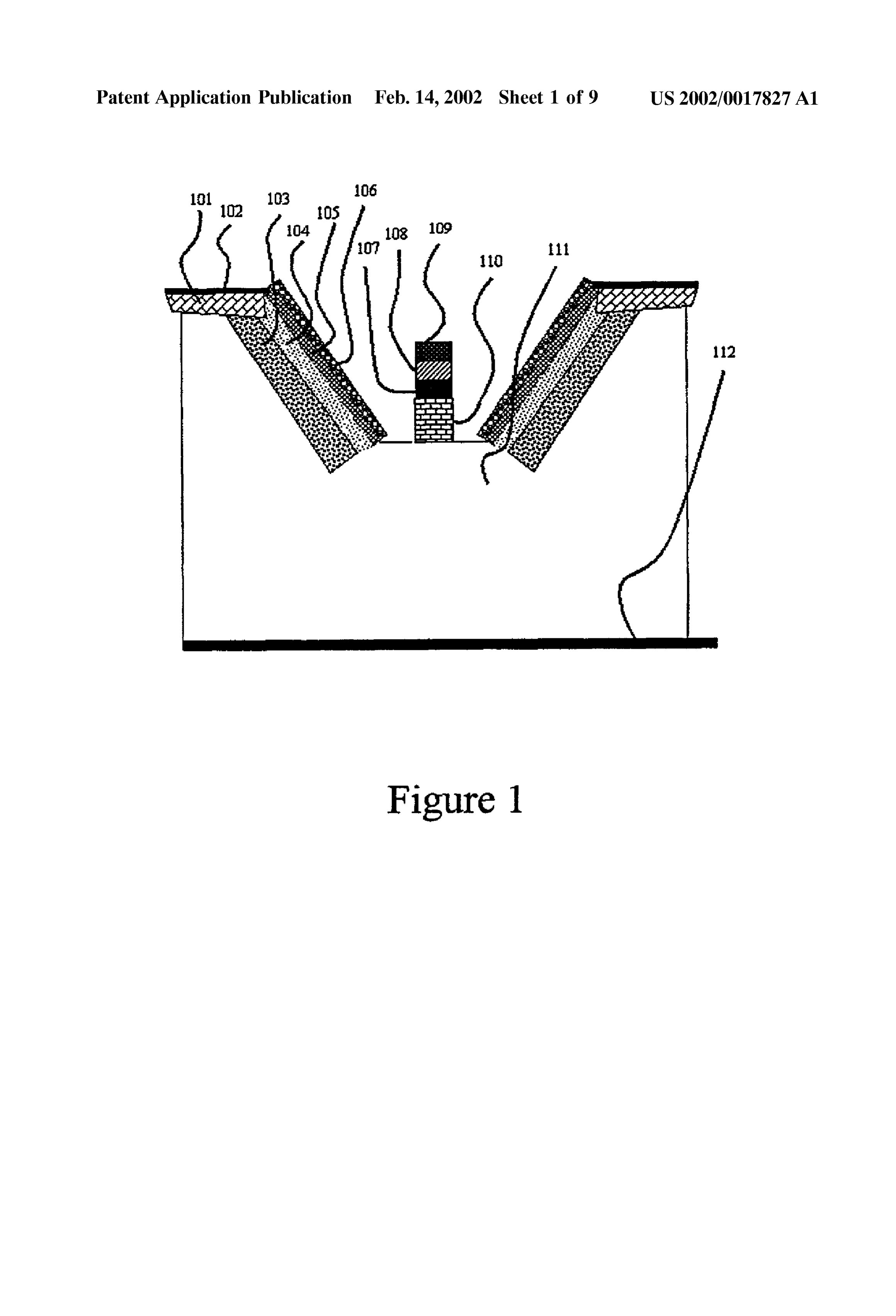
0.035 A sudden onset of high reactivity of the reaction
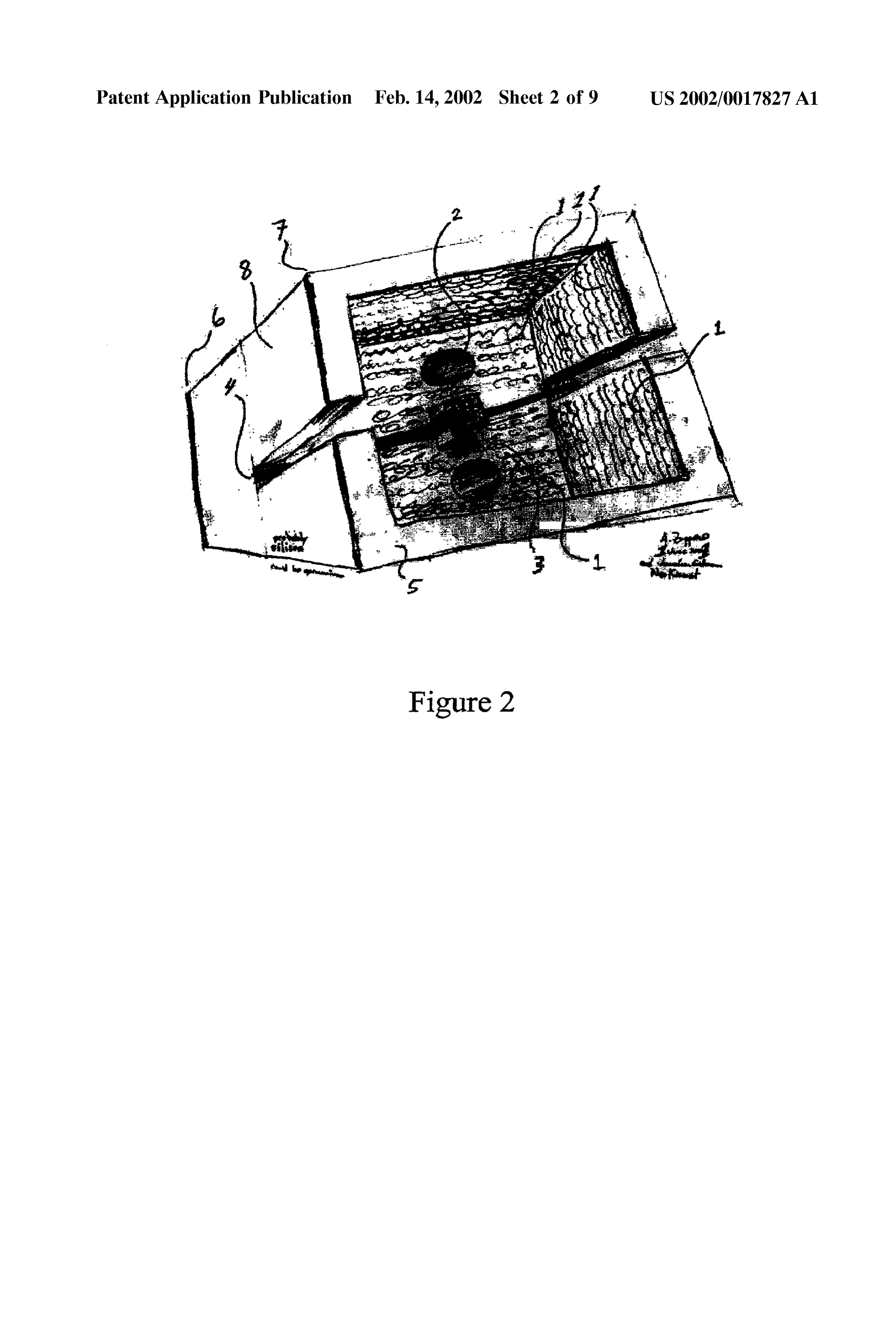
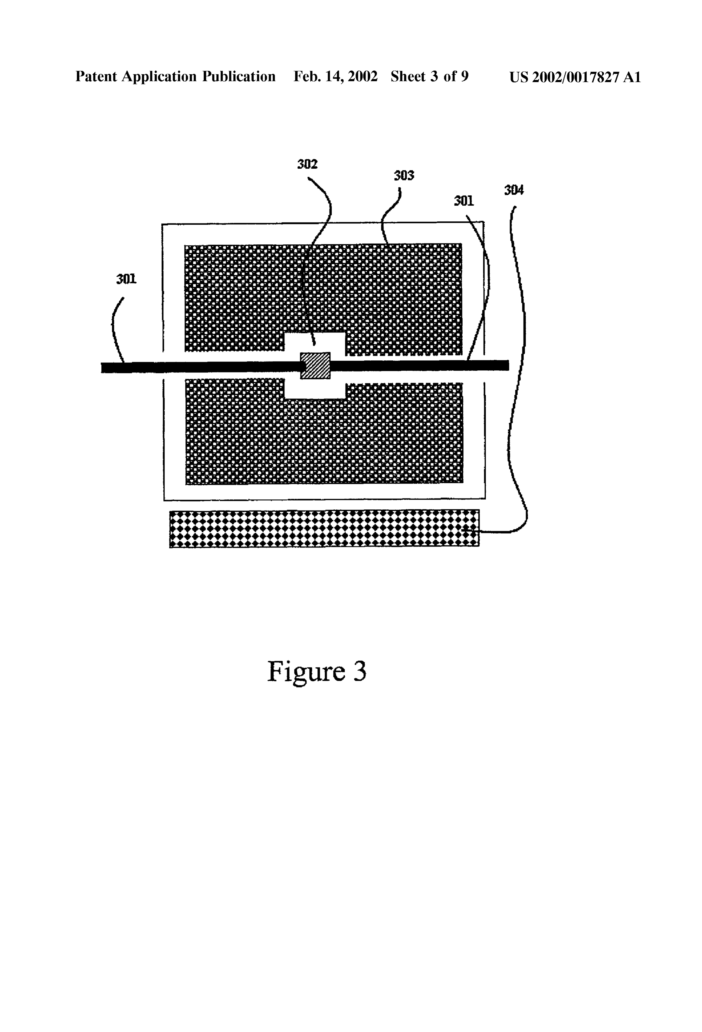
Surface causes a Sudden production of and to Some degree 0044 Preferred embodiments of the present invention desorption of autocatalytic material, resulting in Stimulation will now be described, by way of example only, with of reactions in the gas next to or on the reaction Surface. In reference to the accompanying drawings in which: one embodiment, an initiation is Supplied, where the initia 004.5 FIG. 1 shows a schematic cross section of a tion of chemical reaction between fuel and oxidizer is prompt, for example, taking tens of picoSeconds, and causes gas-phase-reactant-pulsed electric generator using a reaction the sudden onset of this high reactivity between fuel and Stimulator in a V-channel geometry in one embodiment; oxidizer. 0046 FIG. 2 shows the device having a box structure; 0036). In one embodiment, a pulse of energy such as hot 0047 FIG. 3 shows a top view of a gas-phase-reactant, electrons, photons, or phonons, are created and injected into pulsed electric generator using a reaction Stimulator in either a thin reaction Surface. The pulses may originate as optical flat or V-channel geometry;
or electrical pulses. The duration of the pulse is, e.g., Shorter than the time it takes for phonons in the Surface in contact 0048 FIG. 4 shows a schematic top view of a gas-phase with the reactants to equilibrate with the substrate. reactant-pulsed electric generator using a reaction Stimulator in either a flat or a V geometry with a Single fuel port;
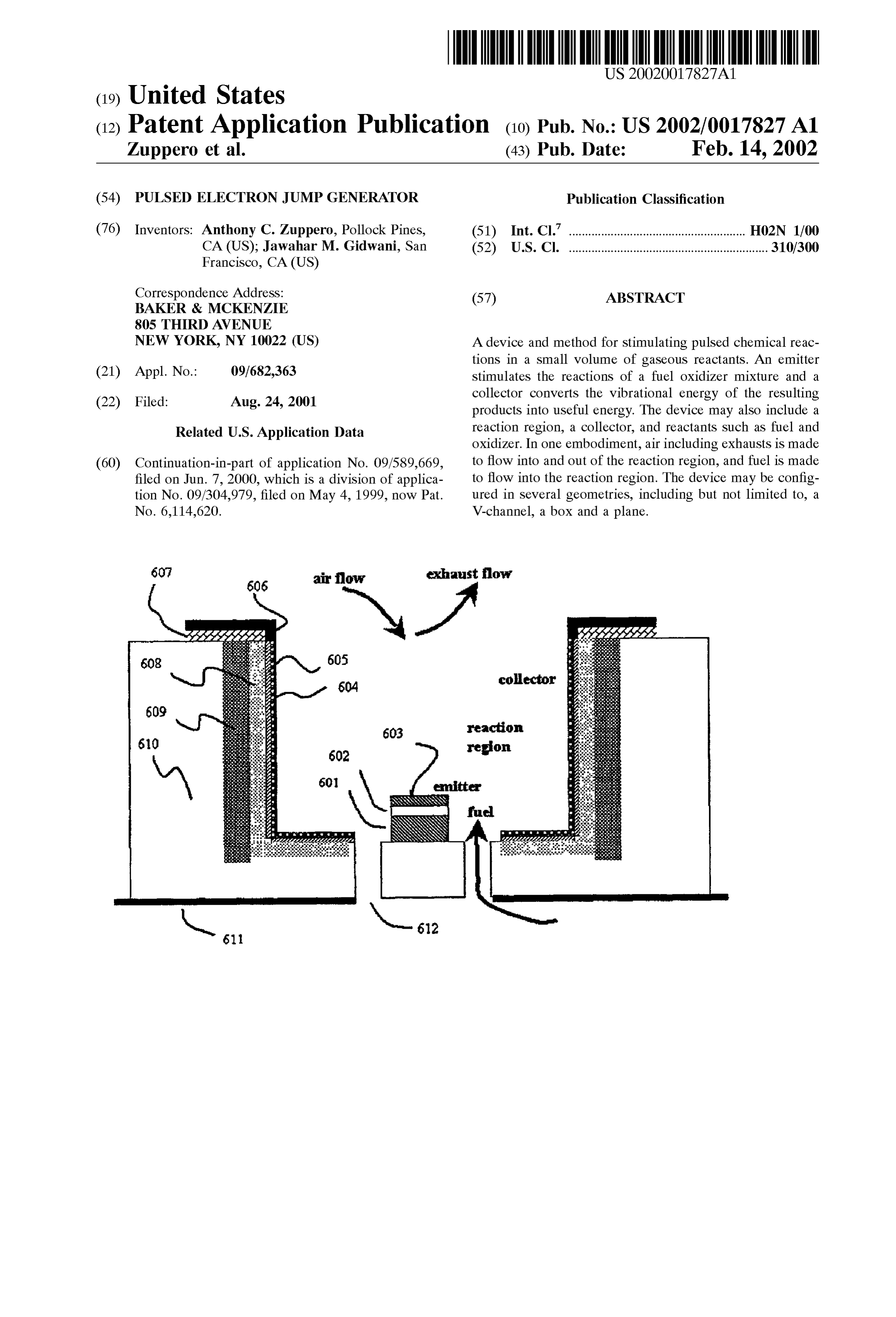
0037. In one embodiment, hot electrons are injected into the thin, nanometers-thick conductive layer to heat the 0049 FIG. 5 shows a gas-phase-reactant-pulsed electric electrons of the conductive layer. This method preferentially generator with emitter Surrounding the collector; heats the electrons faster than heating the vibrations of the 0050 FIG. 6 shows a schematic cross section diagram of conductive layer. The vibrations are heat; the heated elec gas-phase-reactant-pulsed electric generator using a reaction trons are useful. This preferential heating of electrons occurs Stimulator in a box geometry with a fuel port; because the heat capacity of electrons is orders of magnitude lower than that of atomic vibrations, So a given energy input 0051 FIG. 7 shows a transmission line used to drive the heats them orders of magnitude hotter than vibrations. injector of the device of the present invention in one 0.038. In one embodiment, the preferential heating of embodiment;
electrons in the conductive layer may be further enhanced by 0052 FIG. 8 shows an example of composites placed in choosing the thickness of the conductive layers to be of the direct contact with the injector in one embodiment; and Same order of magnitude or less than the energy diffusion parameter of the electrons, which thickness is of order 10 to 0053 FIG. 9 shows a transmission line used to drive an 50 nanometers. emitter injector that is also a collector.
Page 14
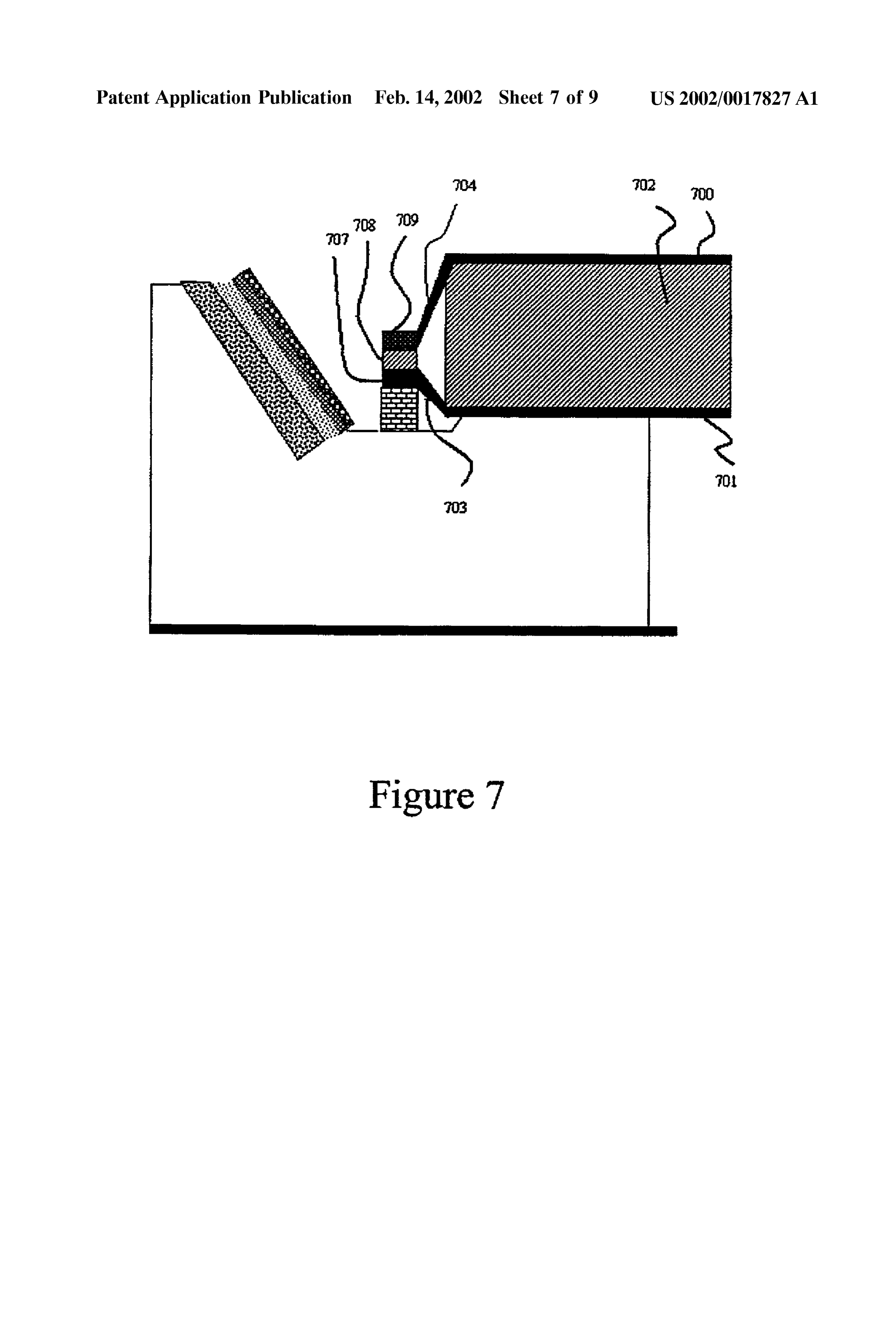
US 2002/0017827 A1 Feb. 14, 2002
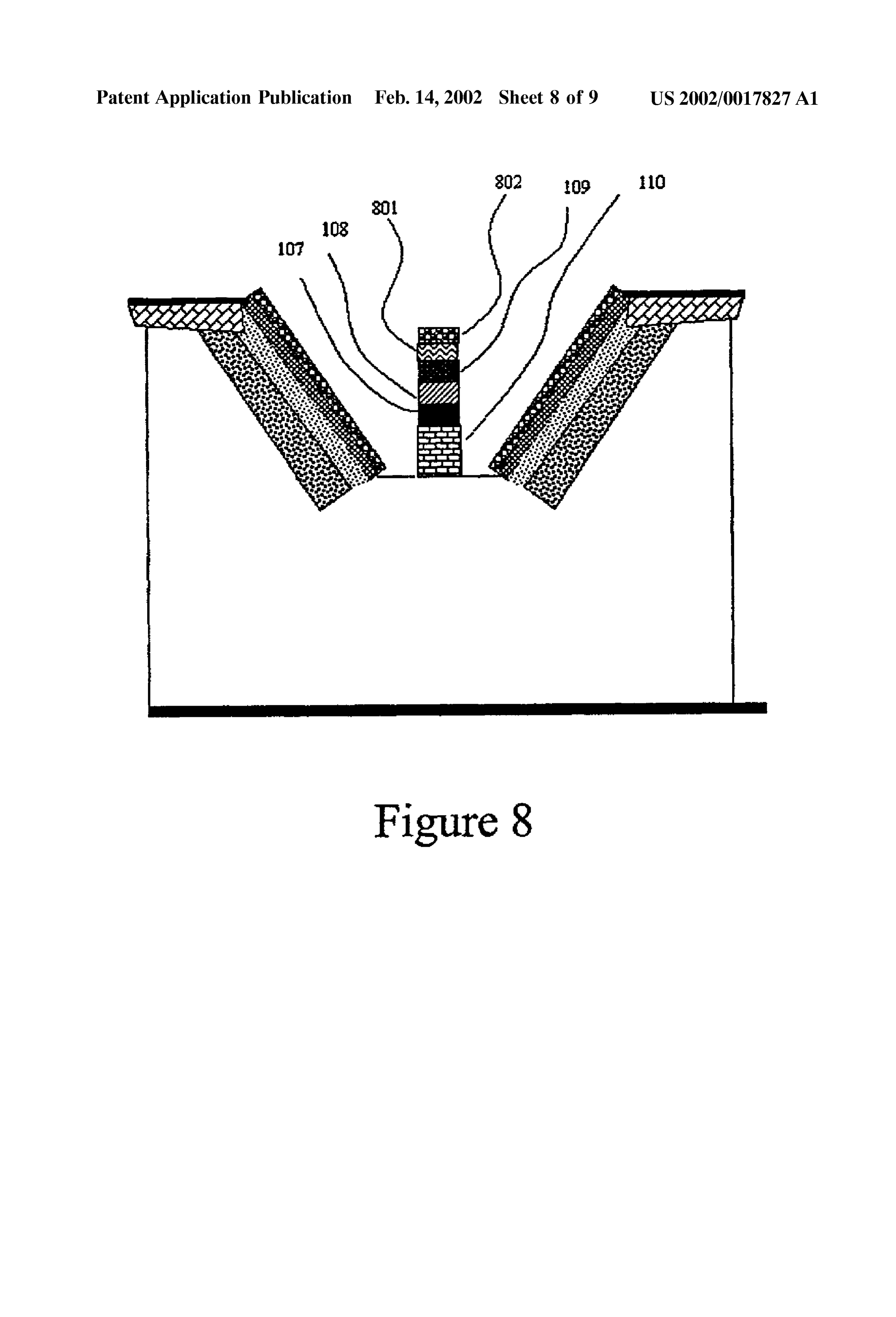
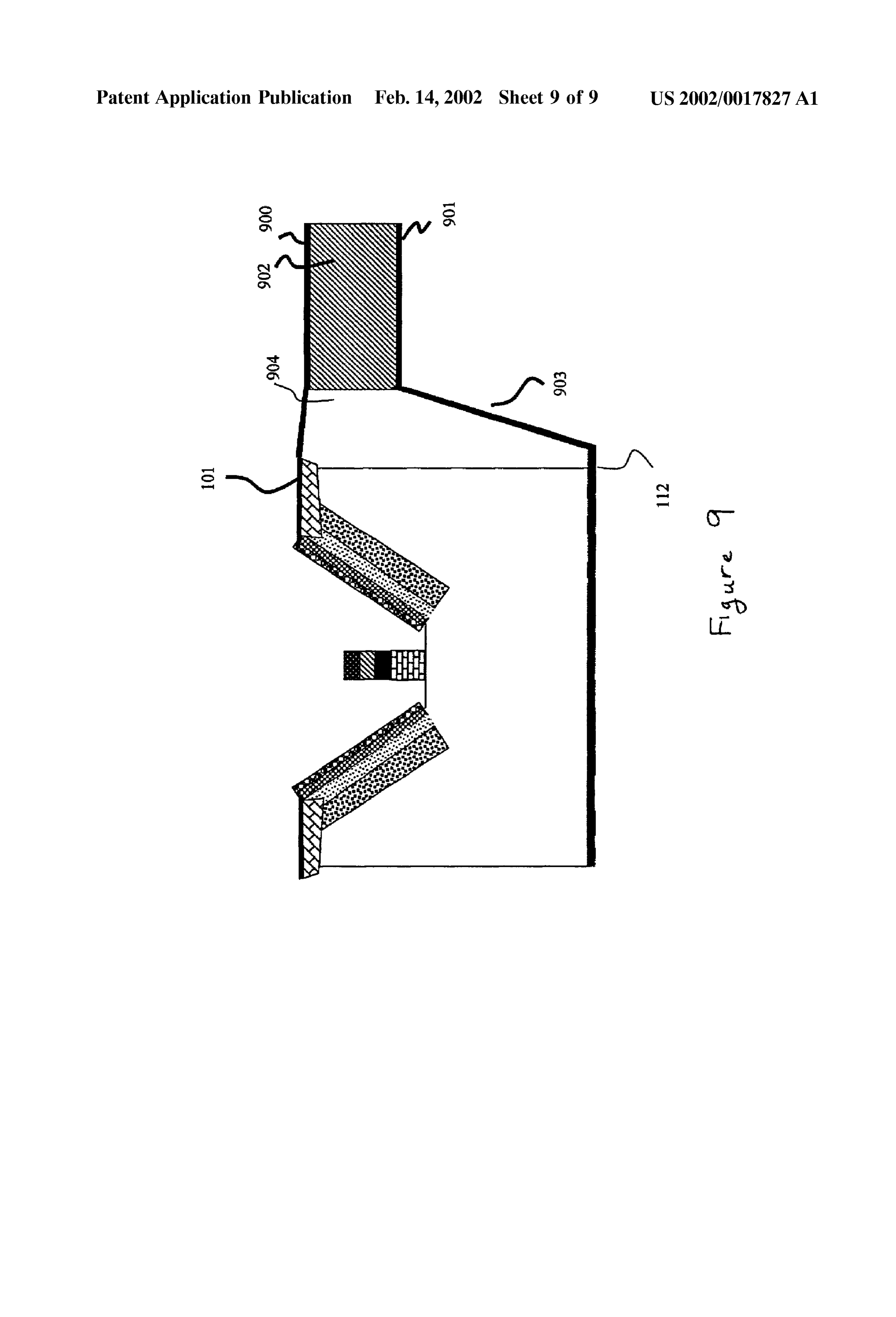
DETAILED DESCRIPTION transmission line, also referred to as a Stripline. This is schematically shown in FIG. 7. FIG. 7 shows a stripline 0.054 FIG. 1 shows a schematic cross section of a gas Superimposed on, e.g., the device of FIG. 1. The electrical phase reactant, pulsed electric generator using a reaction pulse is achieved by driving the Stripline at one end with an Stimulator in a V-channel geometry. Fuel and air mixture electrical pulse across electrodes 700 and 701. The stripline diffuses into the V-channel from above the V-channel. The includes electrodes 700 and 701 and dielectric material 702. emitter includes an electrically-driven hot electron genera The pulse travels from input electrodes 700 and 701 to tor, the hot electron generator also being referred to as an output electrodes 703 and 704. This stripline is a waveguide. injector, Such as a metal-insulator-metal (MIM) injector or a By constructing what is called a dispersive waveguide, by metal-semiconductor-metal (MSM) injector. The injector proper choice of dielectric and electrode properties and includes an electrode 107 formed on a structure 110, e.g., a configurations, a pulse may be narrowed. This transmission heat insulator. In MIM injector a thin tunneling insulator 108 line terminates with its electrodes 703 and 704 by connect is used to provide hot electrons and a thin reaction Surface ing to the injector electrodes 707 and 709. 109, which also may be an electrode, is activated by the injector 108. 0061 Referring back to FIG. 1, when the hot electron injector is designed to be a tunneling insulator, the dimen 0055. In a MSM version a semiconductor 108 is used to sions of the tunneling insulator 108 and thin reaction surface provide hot electrons. A thin reaction surface 109, which 109 are chosen to be of order the same size or less than three also may be an electrode, is activated by the injector 108. times the energy diffusion length of the hot electrons tra The reaction Surface and electrode 109 of both versions
MSM and MIM may use layers and clusters of catalyst and versing the insulator 108, which dimension is e.g., of order tens of nanometers or less in the metal. The term diffusion layerS and clusters of insulator or other material arranged on length of hot electrons refers to the diffusion length of a metal or conducting Substrate, shown as a Single element electrons with the energy appropriate for their use. E.g., a
hot 1 eV electron may degrade into several 0.1 eV electrons.
0056. A pulse of hot electrons is created by applying an The diffusion length for 1 eV electron in a metal is typically electric pulse across the injector electrodes 107, 109. This shorter than that of 0.1 eV electron. Under Some conditions pulse of hot electrons is injected into the thin reaction the diffusion length of an electron in a metal Scales as the surface and electrode 109. The duration of the pulse, e.g., is Square of energy relative to the Fermi level energy. Shorter than the time it takes for phonons in the reaction 0062. In one embodiment, the electrode 109 that receives surface 109 to diffuse away from the thin reaction surface the hot electrons is formed to be thin with dimensions 109. This pulse duration is typically less than 50 picoSec typically of order less than three diffusion lengths of hot onds and greater than 10 picoSeconds. Electrical pulses, e.g., electrons. These electrodes that receive hot electrons may may be of duration approximately 30 picoSeconds to ener include but are not limited to any one or combination of a gize an emitter 107, 108, 109. The length of the pulse is an diode, a metal-insulator-metal device, a metal layer, a metal engineering parameter that depends in part on the degree of layer on a Semiconductor, and a quantum well. These phonon isolation or impedance mismatch between the reac variations of emitter configurations describe different ways tion layer 109 and substrate injector 108. to create hot electrons and render them useful at a reaction 0057. In FIG. 1, injector is shown as an insulator layer Surface.
108 placed between two electrodes 107, 109. The injector 0063. In another embodiment, optical pulses may be also may be, but is not limited to, any one of the following applied to energize the injector. In this case, the injector devices: a forward biased diode, a metal-insulator-metal electrode 107 would not be needed. A similarly thin con device, a Semiconductor-insulator-metal device, a Semicon ductor 109 and an optically thick semiconductor 108 are ductor-metal device, an optical device, or a quantum well. used to receive optical energy generated by an external These injector devices produce a common effect, i.e., the optical generator device. Any known optical generator generation of hot electrons and insertion into a thin reaction device may be utilized. An electrode formed from the thin Surface with, e.g., Sufficiently thin dimension to render the conductor 109 on the semiconductor 108 absorbs the optical hot electrons useful.
energy and creates hot electrons. These hot electrons migrate 0058. The electrically driven forms of the emitter include to the reaction Surface 109.
electrodes such as those shown in 107 and 109, and a 0064. In another embodiment, the reaction surface 109 is reaction Surface 109. In one embodiment, the reaction formed with composites or layers, e.g., an underlayer of surface 109 and the electrode 109 may be one and the same. conductor with dimension less than two diffusion dimen 0059. In one embodiment, to energize the injector elec Sions for hot electrons, and coated with a similarly thin layer trodes 107109, stored electric charges are switched into or of a desirable catalyst. Any desirable catalyst may be used. injected into the injector 107108109. This switching causes Such composites or layerS may be in direct contact with the a forward bias in the diode or injector, further causing the electron injector element (FIG. 1, 107, 108, 109). Stored charges, in the form of hot electrons, to be dumped 0065. An example of composites placed in direct contact into the thin conductive metal electrode 109 which may also with the injector is shown in FIG.8. The composite includes be a reaction Surface. These dumped hot electrons desirably a layer of conductor 801 such as RuO2 with average heat the electrode 109 and the reaction Surface. In FIG. 1, thickness of order 10 nanometers or less, under a catalyst the reaction Surface is shown as the same element as the electrode 109. layer Such as gold or platinum with thickneSS about 10 nanometers or less. Another example of catalysts includes an 0060. In one embodiment, the electrical pulse may be alumina Spiked with Vanadia or other catalysts. When an achieved by electrically driving a transmission line or Strip electrical pulse of order volts is applied to the electrodes 107
Page 15
US 2002/0017827 A1 Feb. 14, 2002
and 109, the fuel and oxygen adsorbed on the emitter 109,801, 802 to be less than about two times the energy 109802 is partially reacted into free radicals or reacted, and diffusion parameter of the electrons, which thickness is of desorbed and delivered into the reaction volume. The reac about order 10 to 50 nanometers.
tion volume is shown in FIG. 1 as the V-shaped channel region between the conducting Surface 106 and the injector 0071. The choice of materials of the conducting layers 107,108,109. The chemical reactions occur in this V-shaped 109,801, 802 may also enhance the heating of electrons. channel region or on the reaction Surfaces in contact with E.g., choosing materials with differing Sound Speeds, or with this region.The Vibrationally excited reaction products may mismatched phonon band frequencies may result in more deposit a Substantial fraction of their vibrational energy into efficient confinement of electron energy. Such choices of an electron of a conducting Surface 106, producing one or materials further enhance thermal isolation and confines the more hot electrons. The reaction products may also include, energy in the electrons.
but are not limited to, photons, vibrationally excited mol 0072 The choice of structures may enhance the confine ecules, and free radicals. ment of hot electrons. E.g., placing the conducting layers 0.066 The catalytic reactivity with respect to reactions 109,801, 802 on pillars, nano-bridges or otherwise raised occurring on the reaction surface 109 (FIG. 1) or 802 (FIG. Structures may also produce more efficient results for elec 8) includes the reactivity associated with the presence of hot tron heating.
electrons on a Surface. Recent experiments have demon 0073 Structures including a small number, e.g. less than Strated that Such hot electrons with temperatures of order 50, of monolayers of dissimilar conductors, e.g. Silver layers 5,000 Kelvin and above have altered the reaction kinetics of on nickel and platinum layers on gold, forming quantum adsorbed species. Experiments showed that hot electrons caused vibrational excitation of the adsorbate Species. confinement of electrons, may also enhance hot electron Experiments showed that as a result of the energy imparted confinement.
to the adsorbates by the electrons, reactions proceeded along 0074. In one embodiment, pulsed hot electron injection paths inaccessible via thermal means, including highly device 107, 108, 109 (FIG. 8) deposits externally supplied endothermic reactions. energy in the conductive layers 109,801, and 802. 0067. The dimension of the channel from the emitter to 0075. The hot electron injection device energizes the the collector defined by a region measured approximately chemicals adsorbed on the emitter Surface and makes them from the geometric center of the croSS Section at electrode act like a Spark plug, triggering reactions in the gas Sur 109 to the center of the collector Surface 106 is of order less than three times the energy diffusion length of vibrationally rounding the trigger or adsorbed on the trigger. The emitter excited reaction products resulting from reaction initiation. operation Starts with Some energy Source creating hot elec This length is of order /2 to 1 micron at Standard temperature trons in an injector. The injector conveys the hot electrons to chemicals adsorbed on the reaction Surface. Hot electrons and pressure (STP) conditions. interacting with chemicals cause chemical reactions. Hot 0068 The collector 106 provides a conducting surface, electrons also case physisorbed adsorbates on a reaction with thickness dimension sufficiently thin to permit the hot Surface to become chemisorbed or desorb, and may also electron to travel through the electrode 105 of the collector cause chemisorbed adsorbates to dissociate on the reaction and into the highly doped p-- region of the Semiconductor Surface or to become physisorbed or desorbed. Some reac 104. The internal field produced by the p+ region 104 and p tions form autocatalyst chemicals, which are highly reactive doped region 103 of the semiconductor tends to draw the chemicals. Some reaction products desorb from the reactive electron to the p region 103. The stronger electric field Surface. The desorbed reaction products typically possess produced by the junction of the p region 103 with the n Sufficient exceSS kinetic energy to initiate reactions in gas doped semiconductor base 111 draws the electron over the molecules. DeSorbed products typically include autocata diode junction. This diode junction is the interface between lysts which are necessary to Sustain chemical reactions Such the p region 103 and the n region 111. In this manner, the as burning and combustion.
diode that includes the p region 103 and n region 111 becomes forward biased, producing a useful voltage acroSS 0076 An example of one energy source creating hot the electrodes 102 and 112. The positive electrode 102 is electrons is an applied Voltage acroSS an insulator or Semi connected to the diode electrode 105 and isolated from the conductor. Another example of an energy Source is a light diode base 111, e.g., n doped Semiconductor base, by an Source, Such as a flash lamp or a pulsed laser beam. insulator 101.
0077. A pulsed hot electron injector may deposit the 0069. The thickness of the base semiconductor 111 may energy in a time that is So short that the hot electron energy be chosen according to engineering needs. The thickneSS or deposits entirely in a nanometers thin reaction Surface, height of the Structure 110 Supporting the emitter may heating it to effective temperatures of thousands of degrees Similarly be chosen and may include raising the emitter Kelvin. This short duration, high intensity pulse of energy more into the V-channel, e.g., one third of the way up from Switches the reaction Surface from an inactive or non the bottom of the V-channel. catalyst State to a highly reactive catalyst State. 0070 Referring to FIG. 8, the input of hot electrons into 0078. The electrons alone may be heated to thousands of the thin, nanometers-thick conductive layer 109 or into degrees. The characteristic time for this is of order 0.5 layers 801 and 802 heats the electrons of the conductive picoSeconds. The phonons or vibrations are heated by the layer faster than heating the vibrations of the conductive electrons, with characteristic times of order 1 to 3 picoSec layer. This heating of electrons over atomic vibrations is onds. The phonons dissipate into the lattice with character enhanced by choosing the thickness of the conductive layers istic phonon diffusion times of order 30 to 50 picoseconds.
Page 16
US 2002/0017827 A1 Feb. 14, 2002
0079 The pulse duration of the pulsed hot electron picoSeconds and ranging even to microSeconds. The hot injector, therefore, may include the use of devices that electron inevitably diffuses into the conductive overlayer produce energy pulses Such as optical or electrical pulses 109,801, 802.
with durations of order less than the phonon diffusion time 0086 To achieve this diffusion, a pn junction semicon in the target conductive layers. The energy pulses Such as ductor with the p side ohmically or almost ohmically optical or electrical pulses impinging on the conductive attached to the reaction surface 109 may be used. The layers 109,801, 802 create the pulse of hot electrons. Semiconductor 108 may include an in type Semiconductor at 0080 A pulsed hot electron injection device of this the junction with the electrode 107 and become and formed invention includes the use of devices that produce either to be p type at the other electrode 109. optical or electrical pulses with durations of order less than 0087. The novel feature of the device includes the ohmic the phonon diffusion time in the target conductive layers. A or almost ohmic contact with the Valence band and demon method of the invention includes using the optical pulse Strates the desirable property of conveying the full, conduc impinging on a conducting Surface 109 to create the pulse of tion band electron energy into the reaction surface 109. hot electrons. A method of the invention includes using an electrical pulse to drive a Semiconductor device or a metal 0088. In one embodiment, a Schottky diode may be used. insulator-metal device 108 designed to inject or transport hot Gold and platinum form desired Schottky junctions with electrons into its positive electrode 109801802 and to drive Silicon, and therefore, may be used to form a hot electron hot electrons from the electrode into the reacting Surface injection diode. Gold has the longer hot electron diffusion 1098O2. length, and therefore, may be more desirable in Some applications. Platinum has the higher catalytic activity, and 0081. The method includes using an optical source of therefore, may be more desirable in other applications. E.g., photons as the primary Source of energy to create hot gold nano-structures have been shown to catalyze the reac electrons. The optical photon energy shall be Sufficient to tion of CO with oxygen, while platinum has been shown to create hot carriers in the semiconductor 108 conduction catalyze the reaction of ethanol and methanol with Oxygen, band. The Subsequent diffusion of carriers drives hot elec and both at temperatures within the operating range of trons into thin conductive layers 109801802 on a semicon silicon, i.e., less than 370 degrees Kelvin. The RuO2 or ductor Substrate. alumina-oxide-metal reaction layer 801, 802 may be depos 0082 yyyyy 1yyyyy1 In one embodiment, the injector ited on the conductive contact 109 of the metal-silicon includes a semiconductor 108 which creates hot electrons Schottky junction 109, 108 as shown in FIG. 8, where the from absorption of light from an external optical Source. In conductor thickneSS is less than three times the diffusion this embodiment, an optical Source with photon energy to dimension of hot electrons Surmounting the Schottky junc create carriers in a semiconductor substrate 108 may be used tion 108-109, and where the conductor 109,802 is selected to irradiate that semiconductor 108 and create hot electrons for convenience.
in its conduction band. The hot electrons So created in 0089. In one embodiment, the pulse of hot electrons heats Semiconductor 108 rapidly, e.g. within tens of picoSeconds, the metal 109 of the Schottky junction and hence heats the diffuse into the reactive Surfaces 109,801, 802. catalysts 801, 802, e.g., RuO2 or spiked alumina, causing 0.083. The semiconductors used in the present invention the catalysts to become highly reactive. Nearly all metals may include those with either direct or indirect band gaps. may form a Schottky junction diode with Silicon. The lifetime of the created hot carriers in the semiconductors 0090. An electrical pulse forward biases the diode 107, with indirect band gaps may be as long as microSeconds. 108, 109, with the negative terminal 107 connected to the Examples of Such Semiconductors with indirect band gaps semiconductor and the positive terminal 109 connected to include but are not limited to Silicon (with band gap of order the diode conductive electrode 109. This diode uses an in 1.12 eV), germanium (with band gap of order 0.66 eV), type semiconductor with a conductive electrode 109. The PbTe (with band gap of order 0.31 eV), and PbS (with band electrode 109 is biased positive and the semiconductor 108 gap of order 0.41 eV). is biased negative. The conductive electrode 109 and any 0084. In semiconductors with direct band gaps, the conductor 801, 802 on top of it is formed with dimension of mobility of the created hot carriers may be high compared to order less than three diffusion lengths for hot electrons. other Semiconductors. The band gap in Such Semiconductors 0091. Upon switching the electrical pulse into electrodes may be engineered. Examples of Such Semiconductors with 107109, the hot electrons surmounting the diode Schottky direct band gaps include but are not limited to In-X Ga-y barrier then flood the positive thin diode conductive elec AS-Z Sb-w, where the band gap can be adjusted over a trode 109 with a pulse of hot electrons. The hot electrons range including 0.1 eV through 1.5 eV. The X, y, z, w values equilibrate with the electrons in the electrode 109 and raise represent the fractional concentrations of each element. the instantaneous electron temperature. 0085. The hot electrons created in the underlying semi 0092. Similarly, in an embodiment having an electrically conductor 108 that move into the conductive overlayer 109, pulsed pn junction diode 107108109, the electrical pulse 801, 802, i.e., a reaction surface 109,801, 802, may become forward biases the diode. In this embodiment, the p side of trapped on the reaction surface 109,801, 802 because the hot the Semiconductor is faced towards the reacting Surface electron lifetime in the Surface is less than tens of femto 801802. An electrical contact 109 is formed to the p type Seconds, which is orders of magnitude Shorter than the Semiconductor So that the conducting electrode forms an lifetime in the Semiconductor. A hot electron in the Substrate almost ohmic junction. Composite catalysts 801802 are 108 has a very long life time by comparison and may diffuse formed in contact with the electrical contact as the reaction through the semiconductor 108 for times exceeding many Surface.
Page 17
US 2002/0017827 A1 Feb. 14, 2002
0093. In an emitter embodiment having electrically allows the two to operate at different temperatures. E.g., the pulsed metal-insulator-metal junctions or Semiconductor collector may include Semiconductor devices that operate insulator-metal junctions for injector, the conductive layer more efficiently at lower temperatures. The emitter may not receiving the electrons that cross the insulator 108 is formed require the use of temperature Sensitive Semiconductors, and Similarly thin, e.g., with dimension of order less than three may operate at higher temperatures for more efficiency. diffusion lengths for hot electrons. In this embodiment, the 0101 Referring to FIG. 7, an initiator pulse is sent into electron transport may be via tunneling through the insulator a transmission line 700701702 to emitter electrodes 707709. 108, passing through its conduction band. Transport may be When the emitter is also a collector and because of the also via electrons with energy greater than the Schottky barrier. The transport may be resonant with adsorbates on pulsed reactions a pulse with more energy than the initiator the reactive Surface can be enhanced by choice of adsorbates pulse is received into the transmission line from the collec tor.
through choices of fuel, oxidizers, and additives.
0094. In one embodiment, electrically pulsed, solid state 0102) The transmission line may also connect to collector optically emitting diodes deliver up to 30 picoSecond dura electrodes. The emitter and collector may be the same tion pulses of photons to a conductive Surface. The diodes physical device. Referring to FIG. 9, an initiator pulse sent may illuminate the Surface from behind, through Substrates into the transmission line 900901902 propagates to its transparent to the radiation emitted by the diode, e.g., as output electrodes 903904 and energize emitter electrodes appropriately chosen material 111108. E.g., a diode emitting 101112. The emitter and collector electrode may be one and 1 eV photons in the infra-red may pass through materials 111 the Same. However, the emitter Stripline may be distinct with 1.5 eV or larger bandgap. Such materials include GaAS, from the collector output System. alumina, or insulators. 0.103 FIG. 2 shows the device having a box structure. 0.095. In one embodiment, the electrically pulsed solid For descriptive purposes only, the device is shown isolated State optically emitting diodes deliver pulse compressed and Standing alone. In practice, a base Semiconductor 8 is optical radiation, using e.g., chirped pulses compressed used to hew boxes 200, resulting in an array of the boxes 200 using dispersive media. Stacked next to one another. E.g., a another of the Semicon ductor base 8 may form an adjacent wall.
0096. In one embodiment, pulses are chosen to have durations less than approximately 10 to 50 picoSeconds, 0104. The fuel is injected or diffused into the reaction depending on injector and reactive Surface material thermal region from the bottom of the device and air diffuses from conductivity and energy transport properties. This duration the top. The collector, emitter, and reaction region elements is approximately the time for the energy deposited by the of this device are similar to those of shown in FIG. 1. The electrons to migrate via phonon heat conduction from the collector 1 forms the inside walls of the box formed out of reactive surface into the underlying injector material 109. the semiconductor 8. Fuel port 2 allows fuel to enter the 0097. Commonly available 30 GHz transistors, radio reaction region inside the box.
frequency pulse generators, magnetic, electrical Storage, and 0105 Having the fuel enter the reaction region inside the pulse compression Systems may be used to produce pulse box permits direct evaporative cooling of the Semiconductor durations satisfying the criteria of less than 10 to 50 pico 8. Direct cooling of the device precisely at the point where Seconds pulse durations. These generators include power heat may be generated and is a novelty of the configuration Signal generators typically used to generate millimeter and permits higher power operation at a given average waves, e.g., those used in Satellite communication or in radar temperature.
pulse generation. Such power Signal generators include gun diodes, vacuum tube devices, klystrons, magnetrons, and 0106 The box geometry is also appropriate when fuel any of many devices currently available to generate pulses and air are fed to the device premixed. In this case the fuel with duration less than approximately 50 picoSeconds. port 2 may be used to feed both fuel and air, or to feed alternate fuels and oxidizers, or as a carburator, or may be 0098. In one embodiment, the pulsed electric generator of eliminated entirely, depending on engineering needs. the present invention includes the emitter 109801802, the energy collector 101102103104105106111112, and a reac 0107 A fuel-rich emitter may also be advantageous. The tion Volume, which is the region between the emitter and the production of autocatalysts may be greatly enhanced by energy collector. In one embodiment, the emitter may be an providing the emitter with a set of chemicals that readily integral part of the collector. In another embodiment, the dissociate and preferentially produce autocatalysts upon hot emitter and the collector may be the same physical device. electron Stimulation. In this case, the fuel port may serve instead as the port for Such additives, Such as fuels and/or 0099 E.g., a semiconductor diode energy converter may oxidizers. This may also serve to permit lean mixtures of be operated in the reverse mode to provide hot electrons to fuel and air, which may also provide a cleaner reaction. its Surface, which may render it an emitter. An advantage of an integral emitter and collector is Simplicity of design. A 0108. The emitter 3 is energized by emitter electrodes 46 pulse applied to the emitter initiates reactions and the and initiates the chemical reaction between fuel and oxi reactions in turn generate electricity in the collector. Thus, dizer. Collisions of the vibrationally excited products with the Same device may initiate reactions and collect energy. the collector wall 1 forward bias the semiconductor 8 that is The result is the equivalent to Stimulating a negative resis connected to negative electrode 6 and positive electrode 7. tance.
0109 FIG. 3 shows a top view of a gas-phase-reactant, 0100. In another embodiment, an emitter and a collector pulsed electric generator using a reaction Stimulator in either may be separate. Having a separate emitter and collector flat or V-channel geometry with the fuel port 304 being
Page 18
US 2002/0017827 A1 Feb. 14, 2002
adjacent to the collector. The fuel port 304 is located to receive and use hot electrons and an injector (FIG. adjacent to the collector 303 and Surrounds the emitter 302 6601602) that generates and provides the hot electrons. The and the electrodes 301. reaction surface (FIG. 6603) includes a conductor and may 0110 FIG. 4 shows a schematic top view of a gas phase optionally include layers of material. The layers of material reactant, pulsed electric generator using a reaction Stimula may include conductors.
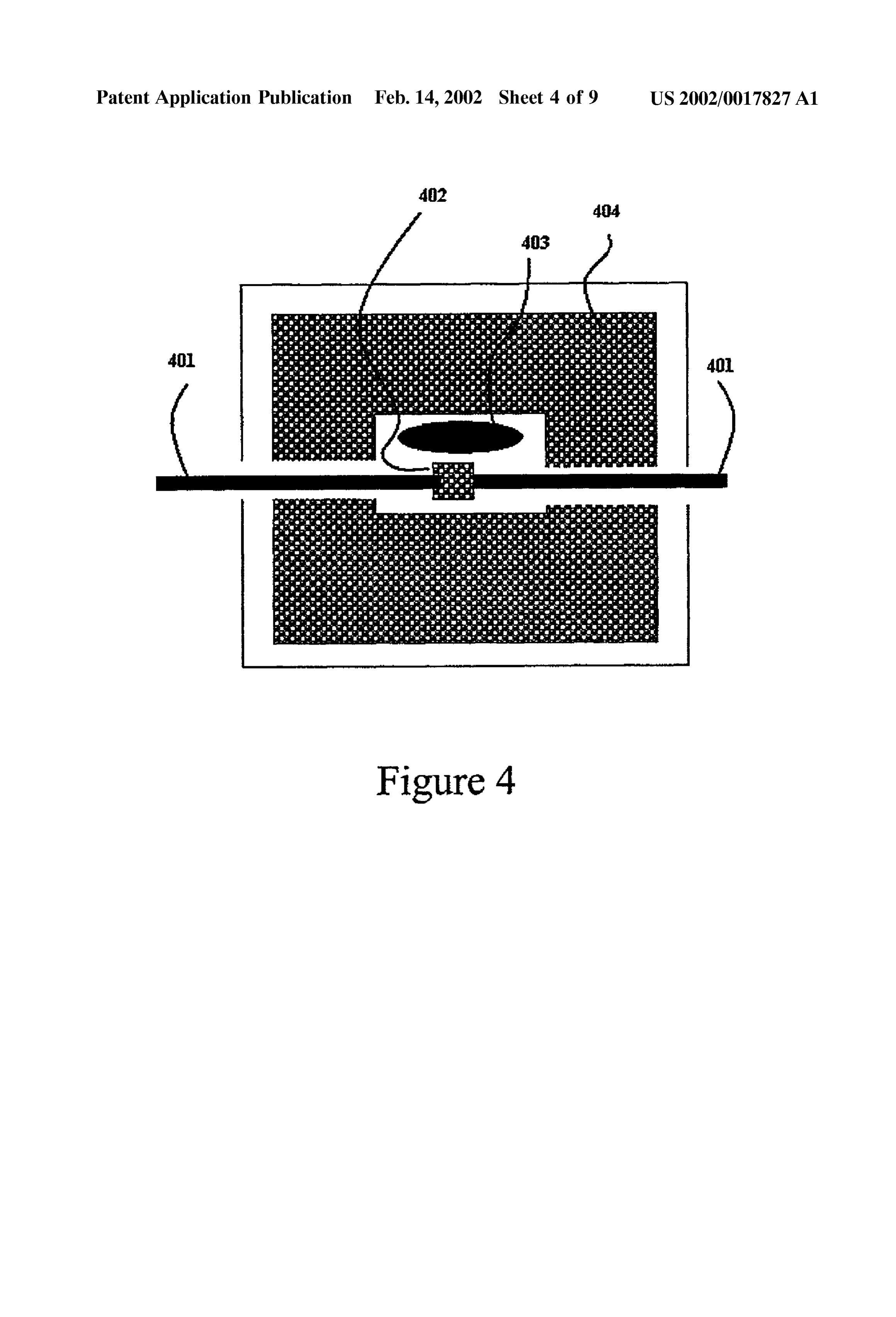
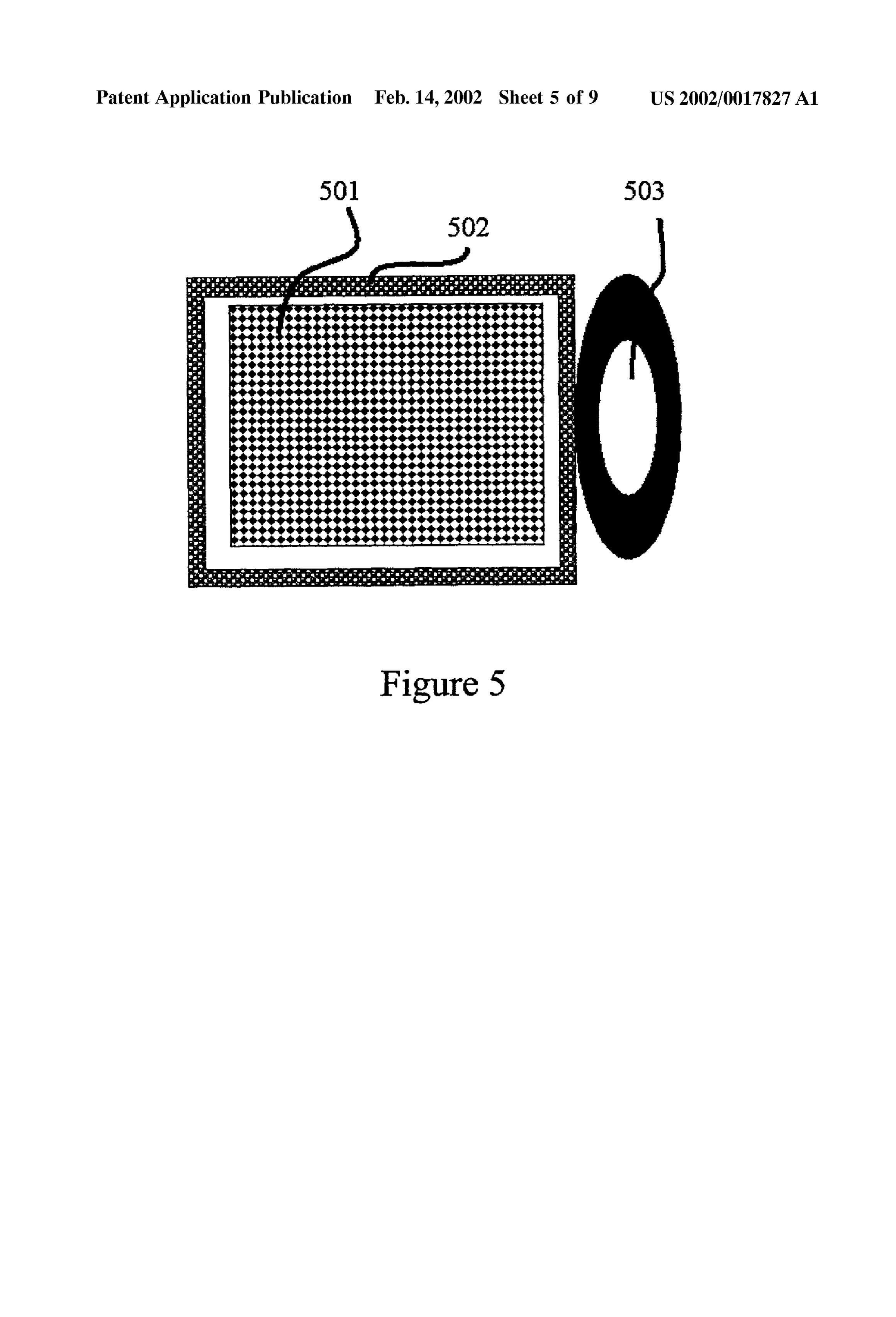
tor in a either a flat or a V geometry with a single fuel port. 0116. The injector produces the hot electrons and injects The gas diffusion process with dimension of order of the them into the reaction Surface. This injector may include but diffusion length for the excited State specie permits flat is not limited to any one or combination of the following geometries to be nearly as efficient as enclosing geometries devices: Schottky diode; pnjunction diode; metal-Semicon Such as the box. Emitter 402 with electrodes 401 are shown ductor-metal device, metal-insulator-metal device, Semicon separate from the collector 404. The reaction region is out of ductor-insulator-metal device; quantum well, optical gen the plane of the drawing. The Substrate Semiconductor erator where the optical radiation impinges directly on the extends into the plane. The fuel emerges from the fuel port thin conductive reaction Surface from behind or from the 403 from the bottom of the device and into the reaction front, optical generator where the optical radiation impinges region above the plane. FIG. 5 shows a configuration similar on a Semiconductor, creating hot carriers in the Semicon to that of FIG. 4, with emitter 502 Surrounding the collector ductor which migrate to a similarly thin conductive elec 501. In this embodiment, a fuel port 503 is located adjacent trode Surface.
to the Structure. This configuration may be repeated over the
Surface of the Semiconductor. 0.117) When the injector, i.e., hot electron producer, 0111 FIG. 6 shows a schematic cross section diagram of 107108 (FIG. 1) is a Schottky diode, the semiconductor gas-phase-reactant-pulsed electric generator using a reaction provides electrons that Surpass the Schottky barrier and travel from the semiconductor 108 into the conductor 109
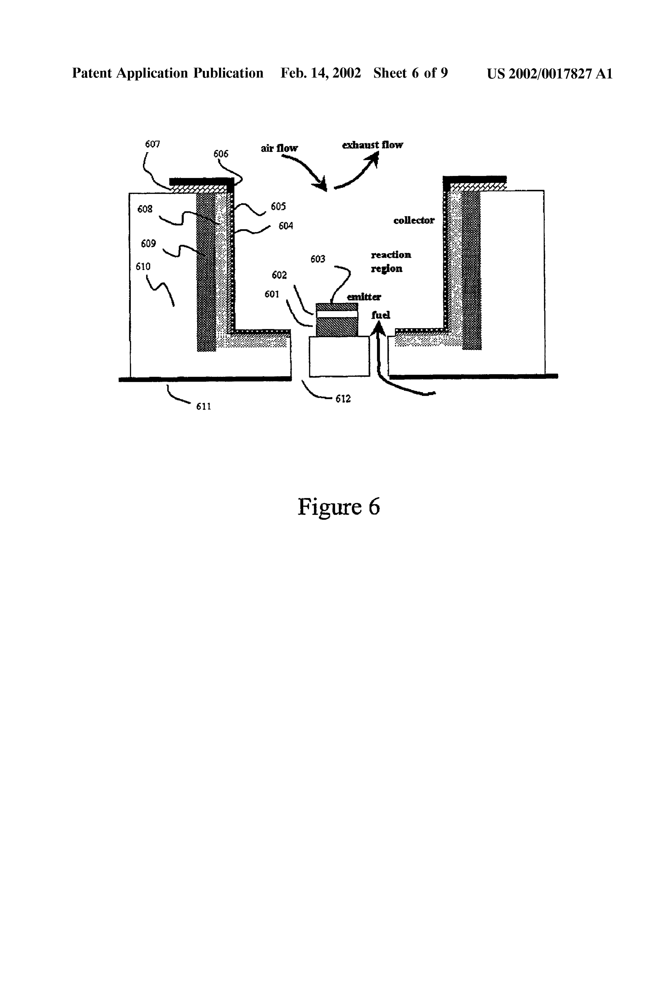
Stimulator in a box geometry with a fuel port, and shows that forms the electrode 109 of the diode. The electrode 109 more detail for the geometry of the device shown in FIG. 2.
The collector includes negative electrode 611, in doped and any materials 801802 (FIG. 8) on the electrode form the reaction Surface.
semiconductor 610, p doped semiconductor 609, p + heavily doped 608, diode electrode conductor 605, collector con 0118 When the injector is a pnjunction diode, the p type ductor surface material 604, positive electrode 606, and Semiconductor provides electrons from its conduction band. electrical isolating insulator 607. Fuel enters from the bot The electrons in this embodiment are minority carriers that tom of the device through fuel port 612. The emitter is travel into the ohmic or almost ohmic electrode 109 and shown with an electrode 601, thin insulator 602, and reactive come in contact with the valence band of the p type Surface 603. A structure under the emitter is omitted to show semiconductor 108. The electrode 109 and any materials that it may be an option to omit the extra Structure. 801802 on the electrode form the reaction Surface. 0112 Fuel port 612 is shown entering in close proximity 0119 When the injector is a metal-semiconductor-metal to the emitter 601, 602, 603, to suggest the option of a fuel or metal-insulator-metal device, one metal 107 is biased rich ignition region and the feature of a cooling of the negative and the other metal 109 is biased positive. Elec semiconductor 610 closest to the hottest element, the emit trons originating in the one metal 107 travel through the ter.
metal-insulator or metal-semiconductor layer 108 and are 0113. In one embodiment of the present invention, semi driven into the other metal 109, biased positive, appearing as conductor diodes are used to collect and convert photons hot electrons in the metal 109. The electrode biased positive into electricity in addition to the hot electrons. E.g., a thin and any materials 801802 on the electrode form the reaction conducting Surface is used to convert the energy of Vibra Surface.
tionally excited molecules into hot electrons. The Semicon ductor diodes are then used to convert the both the photons 0120 When the injector is an optical generator where the and the hot electrons into a forward bias across the diode, optical radiation impinges directly on the thin conductive which generates electricity. reaction Surface 109 either from behind or from the front, 0114 Many geometries of emitter, reaction region, and then the impinging creates hot electrons. The conductive reaction Surface 109 has thickness dimension of order less collector may exhibit useful efficiencies and features. In one than approximately three diffusion lengths for hot electrons. aspect, a spherical collector Surface encloses a spherical reaction Volume with a point emitter in the center, with the The thin conductive reaction Surface and any materials 801802 on the electrode form the reaction Surface. When the radius of the sphere less than three diffusion lengths for injector is an optical generator where the optical radiation Vibrationally excited Specie. The Semiconductor outside the
Sphere is used to form the collector diode. Fuel and air enter impinges on a Semiconductor, the impinging creates hot carriers in the semiconductor 108 which diffuse to an through holes or ports in the Semiconductor. Exhaust leaves the System through ports, holes, or channels in the emitter at appropriately thin conductive electrode surface 109. The the center of the Sphere, for example through a tube or pipe electrode may or may not be deliberately biased using from the center to outside the SphereThe emitter may operate external energy Sources. The electrode and any material 801802 on the electrode form the reaction Surface.
at an higher temperature than the collector. In one embodi ment, the reaction Volume is enclosed in a box with one end 0121 Any known method may be used to energize the open to reactant and exhaust flow. The emitter Structure is injector that generates a pulse of hot electrons. These placed in the center of the box as shown in FIG. 2 and FIG. methods include but are not limited to using devices Such as 6 gyrotrons, microwave power Sources, and regenerative Solid 0115) In one embodiment, the emitter (FIG. 6601, 602, State devices. The regenerative devices include pnpn and 603) in the present invention may include a reaction surface npnp thyristor-type devices. These types of devices include
Page 19
US 2002/0017827 A1 Feb. 14, 2002
light emitting diode Stimulated Zener breakdown Stimula and oxidizer mixtures include but are not limited to fuels torS/accelerators, Stripline pulse compression methods, opti Such as ammonia, oxidizerS Such as hydrogen peroxide, or cal pulse compression methods, tunnel diode, and resonant halogen oxidizers.
transfer devices, Gunn diodes, nano-triodes, and nano 0129. In one embodiment, the reactive species are placed Vacuum tube Systems. into a Volume in direct contact with the conducting Surface. 0122) These energizing devices may be formed integrally The concentration of the reactive species in the Volume may or Separate from the injector device that drives the hot be adjusted So that they become depleted of reactants during electrons into a reaction Surface. The reaction Surface is then the time when the System is in its dead time, e.g., by using heated to temperature in excess of the emitter substrate 109. reactive mixtures in the combustible range or using lean mixtures. Advantageously, fuels adsorb on to many catalyst 0123 The surface to receive hot electrons includes a Surfaces as well as oxygen, So that an optimum fuel-oxidizer conductor 109 with thickness dimension less than three ratio may form on the reaction Surface from a lean mixture diffusion lengths for hot electrons. In one embodiment, the in the gas phase in the Volume. Also during the dead time, surface 109 and the reaction surface 801802 are part of the the Volume may be replenished with more reactive species. Same element. On one Side, e.g., the Side facing the element 108, electrons may be generated and on the other Side, e.g., 0.130. The hot electrons and hot atoms from the products the Side facing the reaction Volume containing the fuel and of the reaction are collected or otherwise used. The products oxidizers, chemical Specie impinge on the Surface are further used to Sustain the duration of high reactivity of 109801802 and adsorb, react or otherwise interact. The the reaction Surface.
thickness dimension is measured from the Side facing react 0131 The radiation emitted by hot atom reactions may be ing gas or materials to the Side interfacing with the injector collected in the form of optical radiation. The optical radia 108. This dimension is generally designed to be less than tion typically results from inverted populations Such as from three times the diffusion length for hot electrons. E.g., this hot atom reactions.
dimension is of order 10 nanometers or more for gold, Silver, and aluminum. 0132) The reacting surface's temperature is raised with out raising the underlying Substrate temperature above 600 0.124. In one embodiment, an optical pulse may be gen Kelvin by using short reaction times and pulses. The tem erated using a flash lamp, electrical gas discharge, optically perature of electrons in the surface is raised to above 5,000 emitting Solid State device, pulsed laser, or pulsed diode Kelvin, and the phonons to above 2,000 Kelvin. The tem laser. The pulse of hot electrons are Stimulated by dumping perature of the Substrate is kept under a temperature that the charge Stored in a capacitor or in the effective capaci would destroy the Substrate’s properties. Such temperatures tance of a Semiconductor junction. are typically under 600 Kelvin. When the temperatures are kept under 600 Kelvin, a substrate would typically maintain 0.125 The pulse durations and dead time intervals are its desirable properties.
tailored to meet the engineering considerations in designing the device of the present invention, including considerations 0.133 While this invention depicts the reaction stimula of thermal heat flow. Pulse durations and dead times may be tion using hot electrons, the invention also pertains to the use longer than microSeconds. E.g., the pulse duration for ener of hot holes. The use of hot holes entails Swapping the gizing is chosen So that the energy collector reaches it reference to electrons with holes, Swapping Valence band for maximum operating temperature and then cooled down to conduction band, and Swapping positive with negative. Such the desired heat Sink temperature during the dead time Swappings between electrons and holes are well known in intervals. the art.
0.126 The dead time interval, i.e., interval between ener 0134) While the invention has been shown and described gizing pulses, is typically Shorter than a time associated with with respect to particular embodiments thereof, it will be the dissociation of precursors to dissociation. This interval is understood by those skilled in the art that the foregoing and typically of order ten nanoSeconds for Oxygen on platinum other changes in form and details may be made therein at room temperature. A precursor is a trapped, intermediate without departing from the Spirit and Scope of the invention. form of an adsorbate as it Successively Surmounts activation barriers towards dissociation on a catalyst or reaction Sur 1. A method of generating energy, comprising: face.
applying a pulse of energy in the vicinity of a reaction 0127. In one embodiment, reactive species are injected Surface to activate the reaction Surface; into the reaction region by Supplying a third specie to the Stimulating reactions in a region Surrounding the reaction emitter, e.g., a fuel catalyst or an oxidizer or a hypergolic Surface to create highly vibrationally excited mol material or a monopropellant or an initiator or reaction ecules, and intermediates or autocatalysts or a mixture of these, in addition to fuel and air, to stimulate the reaction. The third converting the highly vibrationally excited molecules Species dissociate or react to form reaction Stimulators. The created from the Stimulated reactions to useful energy. energizing pulses cause the products of a fuel catalyst 2. The method of generating energy as claimed in claim Supplied to the reacting Surface to Stimulate pulsed fuel 1, wherein the converting includes converting energy of the oxidizer reactions. highly vibrationally excited molecules into hot electrons. 0128. The fuel catalysts may include but are not limited 3. The method of generating energy as claimed in claim 1, further including:
fuel and oxidizer mixtures, unstable specie Such as hydra
Zine, monomethyl hydrazine, or high explosives. The fuel collecting the useful energy.
Page 20
US 2002/0017827 A1 Feb. 14, 2002
4. The method of generating energy as claimed in claim 20. A device for generating energy, comprising: 1, wherein the applying includes applying a pulse of energy an emitter that Stimulates and initiates reactions in pulses, with pulse duration shorter than thrice the time it takes for the emitter having a reaction Surface; energy vibrations on the reaction Surface to equilibrate with its Substrate. a reaction region Surrounding the emitter; and 5. The method of generating energy as claimed in claim a collector near the reaction region, 1, wherein a distance between a reaction Surface and a converter of hot electron energy is equal to or less than thrice wherein fuel and oxidizer reacting near the reaction the aggregate energy diffusion length of electrons generated Surface causes creation of hot electrons, and the col by the pulse of energy. lector converts the hot electrons into useful energy. 6. The method of generating energy as claimed in claim 21. The device of claim 20, wherein the reaction region 1, wherein the pulse of energy includes one or more Selected includes a Surface of the emitter. from the group of hot electrons, photons, and phonons. 22. The device of claim 20, wherein the reaction region 7. The method of generating energy as claimed in claim includes a Surface of the collector. 1, wherein the applying includes applying pulses of energy 23. The device of claim 20, wherein the emitter and the in intervals, wherein the interval between the pulses is collector are on a same Surface. Shorter than a time associated with the dissociation of 24. The device of claim 20, wherein the emitter and the adsorbates. collector are a Same one device. 8. The method of generating energy as claimed in claim 25. The device of claim 20, wherein the reaction region is 1, wherein the method further includes Selecting material formed as a V-channel by the Surrounding collector. reaction Surface with high Sticking coefficient. 26. The device of claim 20, wherein the reaction region is 9. The method of generating energy as claimed in claim partly enclosed by the Surrounding collector. 1, wherein the applying includes applying a pulse of energy 27. The device of claim 20, wherein the emitter includes: in the vicinity of a reaction Surface to create reaction an insulator;
initiators in the reaction Surface, and the Stimulating occurs a first electrode connected to a first Side of the insulator; in response to the reaction initiators in the reaction vicinity and of the reaction Surface.
10. The method of generating energy as claimed in claim a Second electrode connected to a Second Side of the 9, wherein the reaction initiators includes reaction interme insulator, the Second electrode forming the reaction diates. Surface, 11. The method of generating energy as claimed in claim wherein energy pulses can be applied acroSS the first 9, wherein the reaction initiators include reaction autocata electrode and the Second electrode to Stimulate reaction lysts. on the reaction Surface.
12. The method of generating energy as claimed in claim 28. The device of claim 27, wherein the insulator has 9, wherein the reaction initiators include translationally hot thickness dimension that is less than three times the energy Species. diffusion length of hot electrons traversing the insulator. 13. The method of generating energy as claimed in claim 29. The device of claim 20, wherein the emitter includes 9, wherein the method further includes flooding the reaction one or more of a forward biased diode, a metal-insulator Surface with reagents. metal device, a Semiconductor-insulator-metal device, a 14. The method of generating energy as claimed in claim Semiconductor-metal device, an optical device, and a quan 13, wherein the reagents include fuel. tum well.
15. The method of generating energy as claimed in claim 30. The device of claim 20, wherein the device further 9, wherein the reaction initiators are created in pulses with includes a Strip transmission line connected to the emitter for durations less than twenty nanoSeconds. driving energy pulses into the emitter. 16. The method of generating energy as claimed in claim 31. The device of claim 30, wherein the strip transmission line includes a dielectric material in contact with one or 1, wherein the Stimulating includes Stimulating reactions in more electrodes.
a region Surrounding the reaction Surface to create highly
Vibrationally excited molecules near a converter. 32. The device of claim 30, wherein the strip transmission 17. The method of generating energy as claimed in claim line includes a dispersive transmission line designed to compress pulses.
16, wherein a distance between the converter and the region 33. The device of claim 20, wherein the reaction Surface where the stimulating occurs is within thrice the diffusion includes a catalyst.
distance of the highly vibrationally excited molecules. 34. The device of claim 20, wherein the collector includes 18. The method of generating energy as claimed in claim a reaction Surface.
1, wherein the method further includes: 35. The device of claim 20, wherein the emitter includes allowing exhausts formed from the reactions to leave a a Semiconductor whose p side is ohmically or almost ohmi collector Surface; and cally attached to the reaction Surface. 36. The device of claim 20, wherein the emitter includes generating at least one Watt/cm2 of power from the an electrically pulsed Solid State optically emitting diode. reactions. 37. The device for generating energy as claimed in claim 19. The method of generating energy as claimed in claim 20, wherein the collector includes: 2, wherein the hot electrons are transported as carriers in one a conductor Surface;
of Semiconductor and insulator, and cause chemical reac tions to create additional hot electrons. a conductor electrode connected to the conductor Surface;
Page 21
US 2002/0017827 A1 Feb. 14, 2002
a collector Semiconductor connected to the conductor a Schottky diode directly connected to the conductor Surface; and Surface.
a collector electrode in contact with the Semiconductor, 41. The device of claim 20, wherein the collector includes a conducting Surface Supplied with one or combination of wherein the hot electrons created in the collector travel fuel and oxidizer additives.
via the conductor Surface and the conductor electrode 42. The device of claim 20, wherein the collector includes to cause the Semiconductor to become forward biased a conducting Surface with Superlattice Structures. and produces useful voltage acroSS the collector elec 43. The device of claim 20, wherein the collector includes trode. a conducting Surface formed from material with a Debye 38. The device of claim 20, wherein the collector temperature property chosen to optimize the ratio of hot includes: electrons and phonons generated upon exposure to reaction products.
a conductor having a Surface; and 44. The device of claim 20, wherein the collector collects Semiconductor directly connected to the conductor Sur electromagnetic radiation.
face. 45. The device of claim 37, wherein the collector semi 39. The device of claim 20, wherein the collector conductor includes:
includes:
a highly doped p-- region;
a conductor having a Surface; and a p doped region; and a quantum well Structure directly connected to the con a n doped region.
ductor Surface.
40. The device of claim 20, wherein the collector 46. The device of claim 20, wherein the device further includes: includes a fuel port in close proximity to the emitter. a conductor having a Surface; and
Provenance
- Collection
- Patents citing this work
- Original assignee
- Neokismet LLC
- Pages
- 21
- Method
- pdftotext (the PDF's own text layer) + pdftoppm 300dpi page scans
- Patent office record
- patents.google.com →
- Source
- Google Patents citing-documents table
- Inventors
- Anthony Zuppero; Jawahar Gidwani; Neokismet LLC
- Published
- 2002-02-14
- Transcribed from
- patentimages.storage.googleapis.com →