patent · US20030000570A1
Quantum well energizing method and apparatus
2 January 2003
Page 1 — bibliographic record
(19) United States (12) Patent Application Publication (10) Pub. No.: US 2003/0000570 A1
Zupper0 et al. (43) Pub. Date: Jan. 2, 2003 (54) QUANTUM WELLENERGIZING METHOD (52) U.S. Cl. .............................................................. 136,252
AND APPARATUS
(75) Inventors: Anthony C. Zuppero, Pollock Pines,
CA (US); Jawahar M. Gidwani, San (57) ABSTRACT
Francisco, CA (US)
Correspondence Address:
BAKER & MCKENZE A method and apparatus that converts energy provided by a 805 THIRDAVENUE chemical reaction into energy for charging a quantum well NEW YORK, NY 10022 (US) device. The disclosed apparatus comprises a catalyst layer that catalyzes a chemical reaction and captures hot electrons (73) Assignee: Neokismet, L.L.C. and hot phonons generated by the chemical reaction, and an interface layer placed between the catalyst layer and a (21) Appl. No.: 10/185,086 quantum well. The interface layer facilitates the transfer of (22) Filed: Jun. 28, 2002 hot electrons and hot phonons from the catalyst layer into the quantum well layer. The interface layer can also convert hot
Related U.S. Application Data electrons into hot phonons, and Vice Versa, depending upon the needs of the particular quantum well device. Because the (60) Provisional application No. 60/302.274, filed on Jun. hot electrons and the hot phonons are unstable and readily 29, 2001. degrade into heat energy, the dimensions of the catalyst layer and the interface layer are very Small. To improve the
Publication Classification efficiency of the transfer of hot electrons and hot phonons to the quantum well, other interface layers, Such as a catalyst (51) Int. Cl. ............................................... H01L 31/00 interlayer and a catalyst interface, may be utilized.
Lama. T 110
Page 2
Drawing sheet — no readable text.
Page 3
Drawing sheet — no readable text.
Page 4
Drawing sheet — no readable text.
Page 5
Patent Application Publication Jan. 2, 2003 Sheet 4 of 5 US 2003/0000570 A1 Figure 5 ballistic carrier transfer quantum
catalyst or conducting surface
Lic hotelectron diffusion length Figure 6 conducting surface
I.< hotphonon diffusion length
Page 6
Drawing sheet — no readable text.
Page 7
US 2003/0000570 A1 Jan. 2, 2003
QUANTUM WELLENERGIZING METHOD AND Source, Such as optical energy, electrical energy, or thermal APPARATUS energy. There is therefore a need in the art for a method and apparatus for directly energizing a quantum well with a
CROSS REFERENCE TO RELATED primary energy Source. By directly energizing a quantum APPLICATION(S) well with a primary energy Source, the intermediate Step of energy conversion can be eliminated, thus reducing the 0001. This application claims priority to U.S. provisional complexity of the System and improving its efficiency. patent application No. 60/302.274 entitled “Quantum Well
Energizer,' which was filed on Jun. 29, 2001 and is hereby BRIEF SUMMARY incorporated by reference. This application also relates to
U.S. Pat. No. 6,114,620 entitled “Pre-Equilibrium Chemical 0005 The disclosed method and apparatus utilizes a Reaction Energy Converter,” which was filed on May 4, chemical reaction as a primary energy Source to energize a 1999 and is hereby incorporated by reference. quantum well Structure. Chemical reactions that occur on or near a Surface of a conductor or catalyst will emit hot
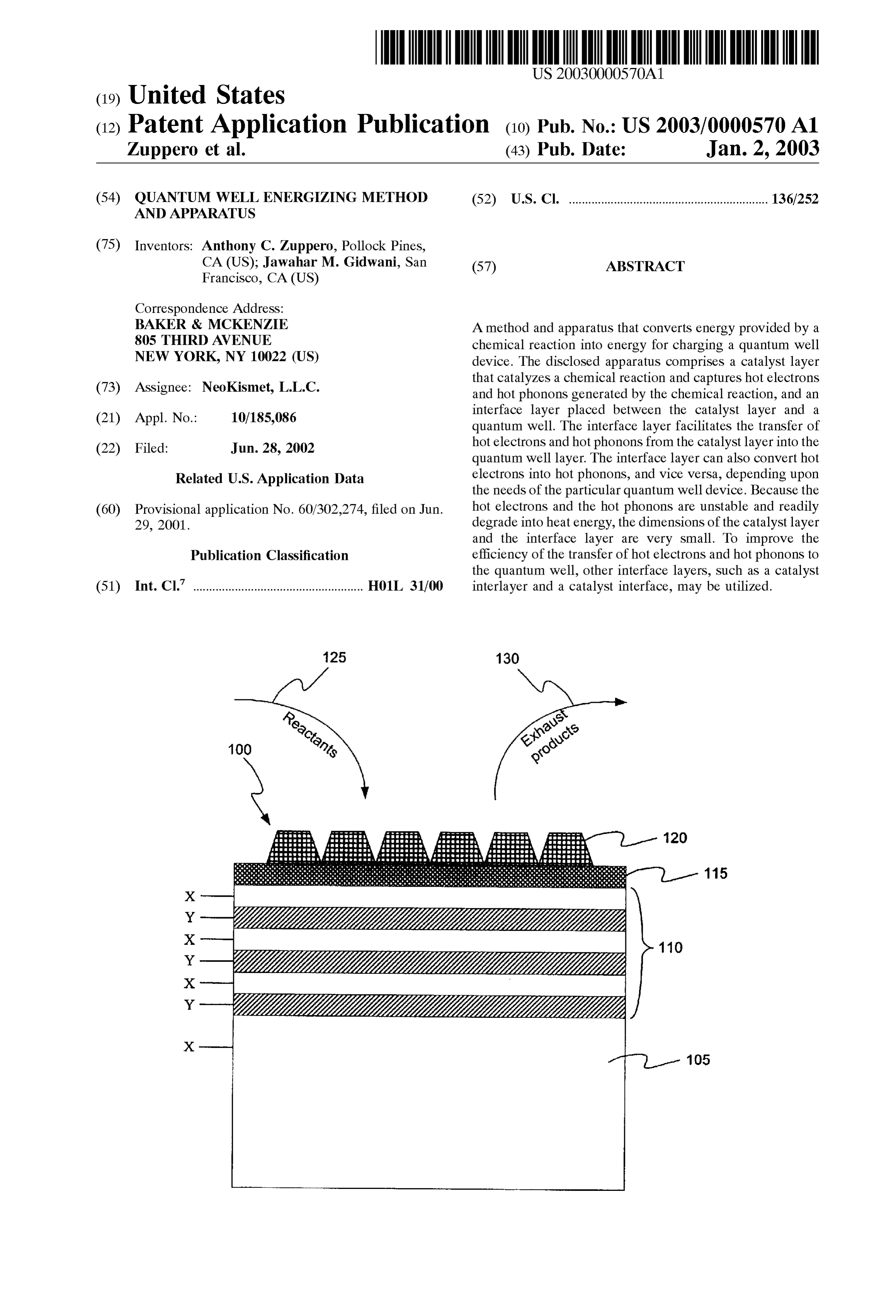
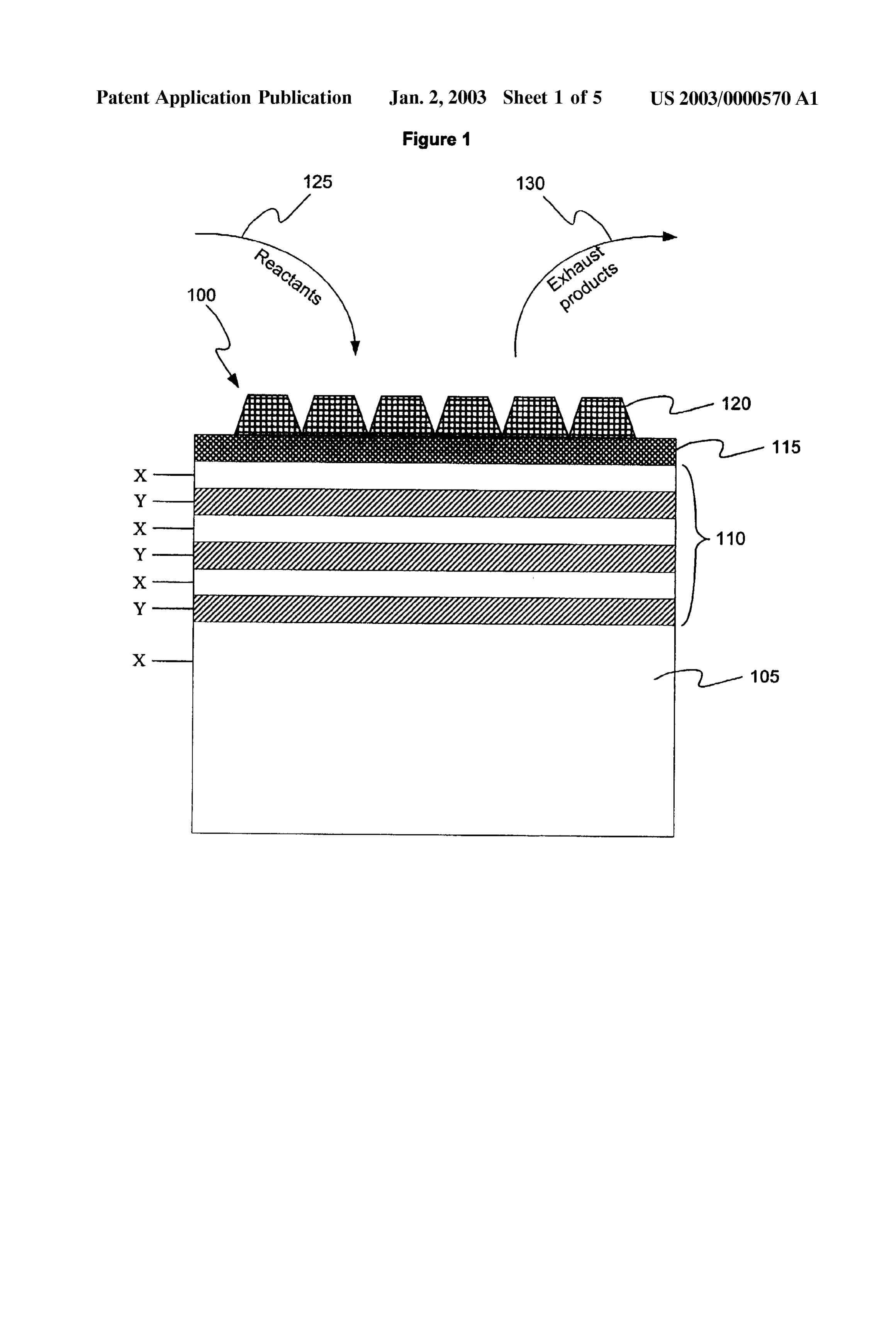
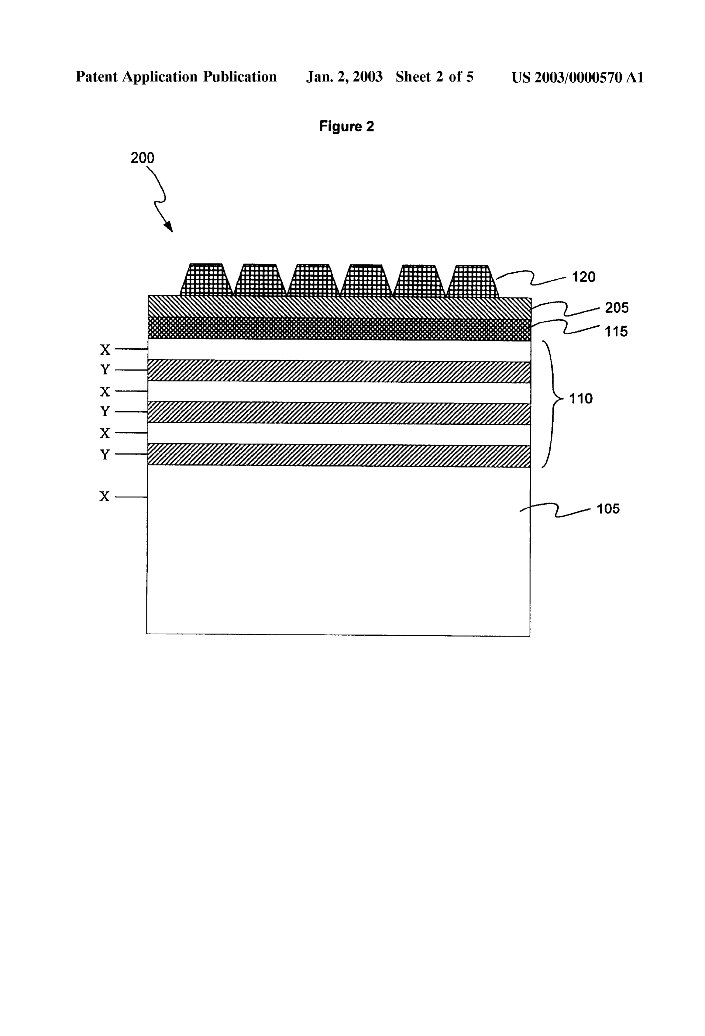
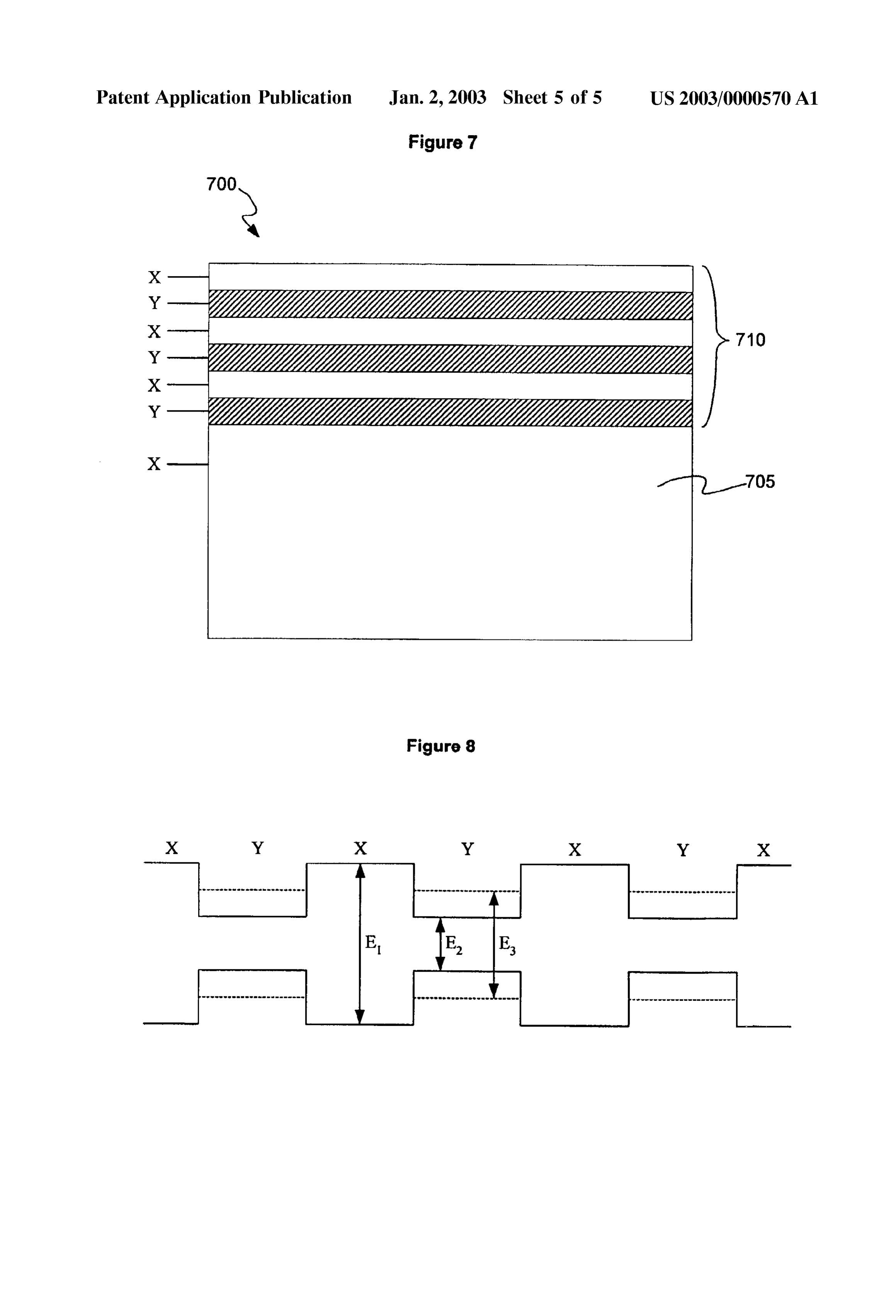
BACKGROUND electrons and hot phonons into the catalyst. It has been determined that a Substantial fraction of the energy released 0002 Quantum wells are solid state electronic devices during certain chemical reactions can be directly transferred that are well known in the art. Among other things, quantum into an adjacent quantum well Structure before that energy is wells can be used to form light emitting diodes (LEDs), converted into heat. This transfer of energy utilizes two Semiconductor lasers, and other tunneling devices. An rep modes: hot electrons and hot phonons. Both of these energy resentative example of a quantum well Structure is depicted transfer modes are effective to pump or energize the quan in FIG. 7. In FIG. 7, a quantum well structure 700 is tum wells. The disclosed method and apparatus utilizes a depicted as comprising a substrate 705 and a plurality of Structure that is a combination of a catalyst layer and an alternating layers 710, (X and Y). Each of these alternating interface layer that are disposed adjacent to a quantum well layers, X and Y, comprises a different composition of device. The catalyst layer catalyzes a chemical reaction on Semiconductor material, thereby creating alternating band its upper Surface and captures the phonons or hot electrons gap diagrams. Although the quantum well Structure 700 in generated by the chemical reaction. The interface layer is FIG. 7 is depicted as comprising multiple layers, it is well disposed between the catalyst layer and the quantum well known in the art that a quantum well Structure may be and facilitates the transfer of the captured phonons and hot comprised of a Several hundred layers, or only one alternat electrons into the quantum well layer. The distance between ing layer, forming a single quantum Well. Although it is the chemical energy Source and a quantum well is preferably usually preferable to use as many quantum wells in a limited to a dimension less than 5 times the energy diffusion quantum well layer as possible, the cost of fabrication can length of the phonons or hot electrons. Accordingly, the limit the number of quantum well that can be economically dimensions of the catalyst layer, interface layers, and the incorporated into the device. The thickneSS and composition quantum wells are very thin. In order to improve the of the alternating layers in a quantum well Structure can be efficiency of the disclosed method and apparatus, the inter varied to produce a variety of other effects. A representative face layer(s) between the catalyst layer and the quantum depiction of the alternating band-gap diagrams created by well can facilitate the conversion of hot electron energy into the alternating semiconductor layers 710 is illustrated in desired phonon modes, especially longitudinal optical FIG 8. modes. The interface layerS may also be arranged to convert 0003) In FIG. 8, the band gap for each of the layers phonons into hot electrons, as the need arises. alternates between a large band gap E, which corresponds to the band gap of material X, and a Smaller band gap E, BRIEF DESCRIPTION OF THE DRAWINGS which corresponds to the band gap of material Y. The 0006 FIG. 1 is a cross-sectional diagram of one embodi juxtaposition of these two layers at very Small dimensions ment of a quantum well energizing apparatus Suitable for use causes the distance between the conduction band Fermi level with the disclosed invention.
and the valence band Fermi level in material Y to be widened from energy level E to energy level E. This widening 0007 FIG. 2 is a cross-sectional diagram of an alterna allows the quantum well to perform as if it were operating tive embodiment of a quantum well energizing apparatus as a different kind of material with a wider band-gap. Suitable for use with the disclosed invention. Accordingly, when properly pumped and Stimulated, quan tum well devices can emit light at wavelengths that would 0008 FIG. 3 is a schematic diagram depicting the pro not normally be associated with typical Semiconductor mate ceSS by which hot electrons may be generated by a chemical rials. These devices can therefore provide great utility for a reaction on a catalyst Surface.
wide variety electronic devices. 0009 FIG. 4 is a schematic diagram depicting the pro 0004 One problem associated with existing quantum ceSS by which hot phonons may be generated by a chemical well Structures relates to how the quantum well is energized reaction on a catalyst Surface.
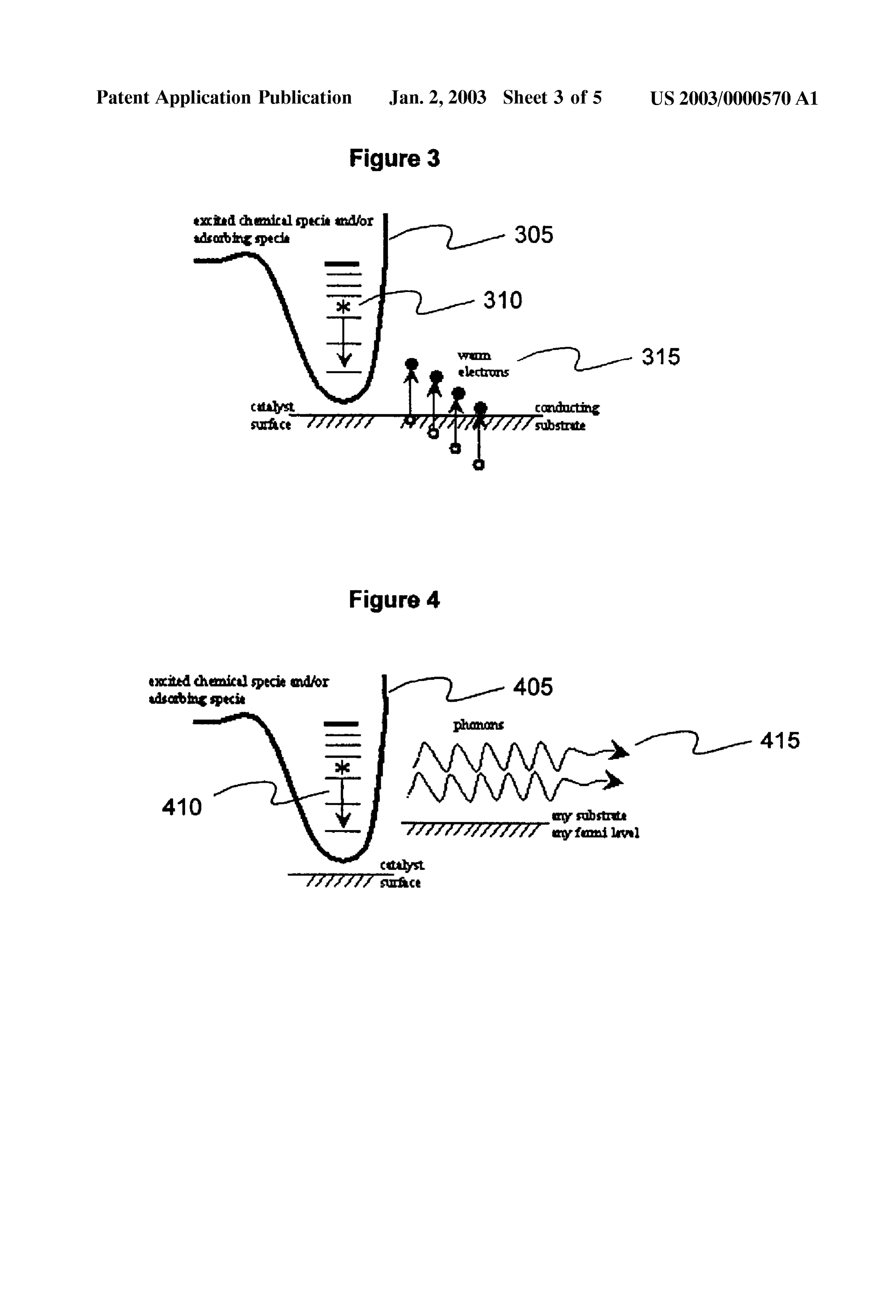
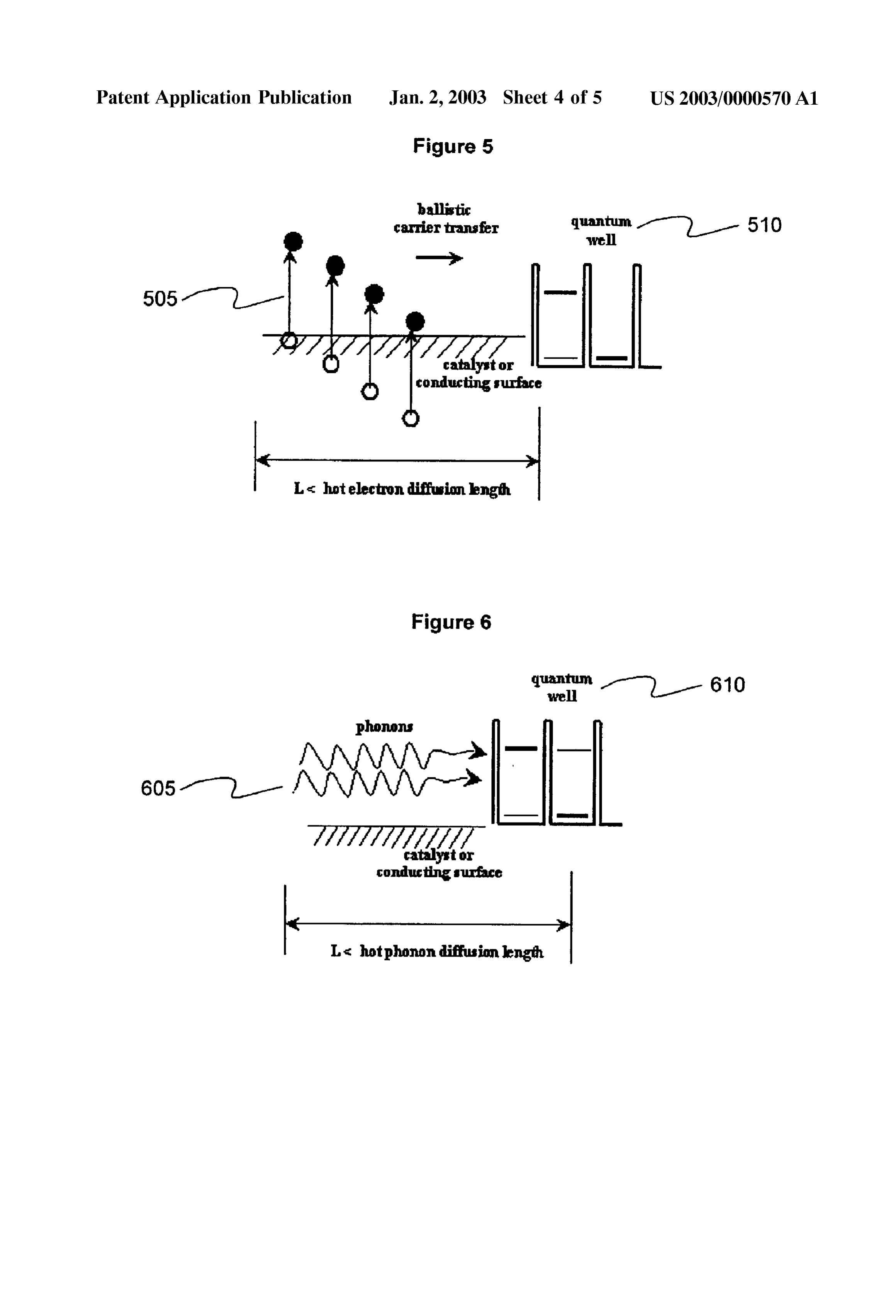
(i.e. pumped). Existing methods for energizing a quantum 0010 FIG. 5 is a schematic diagram depicting the pro include applying an electric field across the quantum well, ceSS by which hot electrons may be injected into and thereby optically pumping the well with photons of Sufficient energy energize a quantum well device.
(i.e. wavelength), and thermally pumping the well with a heat Source and a cold sink to induce a population inversion. 0011 FIG. 6 is a schematic diagram depicting the pro These methods are undesirable because they require a step ceSS by which hot phonons may be injected into and thereby of converting primary energy into an intermediate energy energize a quantum well device.
Page 8
US 2003/0000570 A1 Jan. 2, 2003
0012 FIG. 7 is a cross-sectional diagram of a represen 0018. An important feature of the interface layer 115 is its tative quantum well device. ability to convert hot phonons and hot electrons into energy 0013 FIG. 8 is a band-gap diagram of the representative forms Suitable for charging the quantum well. In particular, quantum well device depicted in FIG. 7. it is desirable for an interface layer 115 to be able to convert hot phonons into energetic carriers, also known as electron
DETAILED DESCRIPTION hole pairs (EHPs), that can be stored in the quantum well. This kind of energy conversion is known as phonon cou 0.014. The disclosed method and apparatus relates to a pling. Examples of Semiconductor materials that exhibit Structure for catalyzing a chemical reaction to provide hot favorable phonon coupling properties include GaN, SiN, electrons and hot phonons to energize a quantum well SiC, GaAS, AIAS, and the family InGaASSbw. According Structure. Chemical reactions that occur on or near a Surface, to a preferred embodiment, material X comprises Gallium Such as a conductor or catalyst, will emit hot electrons and Nitride and material Y comprises a mixture of Gallium hot phonons into the catalyst. It has been determined that a Nitride and Aluminum (AlGaN). Other pairs of semicon Substantial fraction of the energy released during certain ductor layers that may function as interface layers include, chemical reactions can be directly transferred into a quan for example:
tum well Structure before that energy is converted into heat. 0019 GaAs/All and GaAs,
Our theoretical models have indicated that a majority of the energy produced by a chemical reaction can be used to 0020) Al-GaN and AlN;
energize a quantum well, depending upon the Specific device characteristics. The transfer of energy from the chemical 0021 Al-GaSb and AISb;
reaction to the quantum well utilizes two transfer modes: hot electrons and hot phonons. Both of these energy transfer 0022 ZnS, Se, and ZnS; and modes are effective to pump or energize the quantum wells 0023 SiGe and Si.
with charge carriers.
0.015 The disclosed apparatus and method uses a catalyst 0024. According to a preferred embodiment, the follow layer and one or more interface layers to produce hot ing compounds can also be used for the interface layer: phonons or hot electrons that can be injected directly into a GaAs/Al, and Gaoss ASons or Siolo, Geolos and Si. Materials quantum well. To accomplish this task, the distance between such as Pb and diamond, with vastly different phonon bands the chemical reaction site and the quantum well is preferably and conductivity properties, for example, may also be used less than 5 times the energy diffusion length of the phonons in the interface layers. Pb and diamond are representative of or electrons. the extreme of physical properties and show that any mate rial may be considered a candidate material for these pur 0016 A variety of factors may be considered when poses. Bipolar Semiconductor materials composed of ele Selecting and arranging the materials of the disclosed appa ments of different masses and crystal structures (e.g. ratus, Such as the electronic properties, phonon band prop Wurtzite and zinc-blende) may be used, Such as alloys and erties, crystal Structure, and the lattice constant of the III-V and II-VI semiconductor compounds. Accordingly, a Substrate, interface layers, and the quantum well. Further wide variety of compositions and thickness may be Selected more, the electrochemical properties of the catalyst layer and to provide for a desirable balance between bandgap differ its relationship to the interface layers can affect the Selection ential, crystal dimensions, lattice constants and phonon-EHP of the composition and dimensions of the catalyst layer. coupling. The compositions described above may also be Another aspect of the invention relates to the Selection of used to form the Substrate layer 105. reactants to produce the hot electrons or phonons in the 0025. A quantum well interface layer 115 is placed adja chemical reaction.
cent to the quantum well structures 110. The quantum well 0.017. A representative embodiment of a quantum well interface 115 is used to match the material and electronic energizing apparatus 100 suitable for use with the invention properties of the catalyst layer 120, or another interface is depicted in FIG.1. In FIG. 1, a quantum well energizing layer, with the quantum well 110. The quantum well inter apparatus 100 is depicted as comprising an interface layer face layer 115 is also used to convert and tailor phonon or 115, and a catalyst 120. Also depicted in FIG. 1 are a carrier energies to make them useful in the quantum well. In substrate portion 105, a quantum well layer 110. The inter addition, the materials comprising the quantum well inter face portion 115 may comprise any of a variety of Semicon face can be used to convert hot electrons or hot phonons into ductor-related materials, including, for example, Silicon, the desired energy mode. In this manner, the efficiency of the Aluminum, Antimony, Gallium Arsenide, Indium PhoS process can be improved. According to one embodiment, the phide, and any combination thereof. According to a pre quantum well interface 115 comprises a composition of ferred embodiment, the interface layer 115 comprises type Gallium Nitride (GaN) or Aluminum Gallium Nitride (Al IV, III-V, or II-VI compositions such as Silicon, Gallium GaN). It is known that these compositions have strong hot Arsenide (GaAs), Gallium Nitride (GaN), Gallium Phos electron-phonon coupling and therefore will convert a phide (GaP) and SiC. For purposes of illustration, however, large number of the hot electrons passing through it into the interface layer 115 will be referred to as comprising phonons. Another purpose Served by the quantum well material X. Disposed adjacent to the interface layer 115 is interface 115 is to match the electrical and structural prop one or more quantum well structures 110. In FIG. 1, six erties of the quantum well devices with the catalyst layer alternating layers are depicted as comprising material X and 120, or other adjacent interface layer. The thickness of the Y. AS described above, the composition and thickness of quantum well interface layer 115 is limited by the mean free these alternating layers are Selected So that the band-gaps of path of the energy modes passing therethrough. Specifically, each respective layer form one or more quantum wells. the intermediate layerS Should be arranged Such that the
Page 9
US 2003/0000570 A1 Jan. 2, 2003
distance from the catalyst Surface 120 to the quantum well the AlGaN alloy and therefore may not efficiently transfer layer 110 is less than about five times the energy mean free the emissions energy to the quantum well layer. To over path. come these incompatibilities, a catalyst interlayer 205 com 0026. The catalyst 120 comprises a layer of metal, semi prising a metallic Substance, Such as Aluminum, can be conductor or insulator that catalyzes a chemical reaction on placed between the catalyst 120 and the quantum well interface 115 So as to form an ohmic contact between with its Surface. A wide variety of materials have been found the AlGaN alloy and the Platinum catalyst and thereby Suitable as catalysts 120 including, for example, aluminum, facilitate the injections of hot electrons and hot phonons into platinum, palladium, rhodium, ruthenium, and transition the quantum well. A catalyst interface layer (not shown in metals. Insulating materials, Such as RuO2, Alumina FIG. 2) may also be incorporated between the catalyst layer (AlO4), Titania (TiO), and Vanadia (VO), have also 120 and the catalyst interlayer 205, depending upon the proven effective as catalyst layers. The insulating materials materials and energy transfer modes utilized by the device. generally only produce hot phonons or hot holes during the The catalyst interlayer 205, however, may only be needed to chemical reaction. Accordingly, the mean free paths for match the phonon coupling properties and the crystal Struc these energy modes are much shorter than those for hot ture properties of the catalyst layer 120 and the catalyst electrons. Other materials that form Suitable catalysts interlayer 205. Further alternative embodiments are contem include one to ten monolayers of Gold (Au) deposited on plated for the disclosed invention, including an apparatus in oxide insulators, such as Titania (TiO), Iron Oxide (Fe2O), which the catalyst interlayer 205, the catalyst interface 110, or Co-O. The catalyst layer 120 is preferably arranged such and the quantum well interface 115 are incorporated into a that a plurality of clumps are present on the Surface of the Single layer. According to another embodiment, these inter catalyst 120. These clumps may take a variety of forms face layers can be Superlattices formed from combinations including, for example, islands, corrals, chaotic Surface of conductors, insulators and Semiconductors. constructs, pyramids, layers, monolayers and monolayered islands. Each of these structures are formed with dimensions 0029. The chemical reaction that occurs on the surface of in the range of 0.3 to 20 nanometers. The lower boundary for the catalyst layer 120 includes intermediate reactions that this range, 0.3 nanometers, represents one monolayer (i.e. form products that ultimately result in exhaust products. one atom) thickness for the catalyst. The upper boundary for This concept is illustrated in FIG. 1, where reactants 125 are this range, 20 nanometers, represents the upper end of the applied to the surface of the catalyst layer 120 and exhaust mean free path for hot electrons and hot phonons. 20 products 130 are discharged and removed from the surface nanometers roughly corresponds to about 100 monolayers. of the catalyst layer 120. The process of removing exhaust The catalyst 120 catalyzes a chemical reaction So as to products is important for two reasons. First, as exhaust produce hot phonons and/or hot electrons. According to products are removed from the surface of the catalyst 120, well-known chemical theory, these reactions are Strongly they permit additional reactants to be adsorbed on the catalyzed at the edges and corners of the catalyst Structures catalyst Surface 120, thereby ensuring that a continuous 120. Thus, by increasing or decreasing the number and size reaction occurs. Second, the removal of exhaust products of the edges in the catalyst Structure 120, the degree to which from the surface of the catalyst 120 dissipates heat from the the reaction is catalyzed can be adjusted. catalyst layer 120. Heat dissipation is important because the 0.027 Recent research has shown that during a brief time disclosed chemical reactions can generate as much as period after the catalyzation of a chemical reaction, charge 10-100 watts/cm on the surface of the catalyst layer 120. carriers, Such as hot electrons and hot phonons are emitted 0030 The chemically excited products produced by the by the reaction. These emissions, also known as "pre chemical reaction include intermediate reaction products, equilibrium’ emissions, are captured by the catalyst layer the exhaust products of chemical reactions, dissociated 120 where they can be passed into the interface layer(s) 115 adsorbates, precursor States of adsorbates on a catalyst or and eventually into the quantum well 110. These emissions conductor Surface, hot atoms, and the adsorption reaction are unstable and will readily transform into heat or other products of chemicals with a Surface. Intermediate reactions non-productive forms of energy in brief periods of time (tens also release pre-equilibrium hot electron-hole pairs (EHPs) of picoSeconds or less). Accordingly, it is desirable that the and hot phonons. These emissions are known to energize catalyst layer 120 be located close to the quantum well layer phonon modes in the interface layer 115, the quantum well 110 So that the emissions can be used to energize the 110, and even the Substrate 105. quantum wells 110 before they degrade into heat.
0031. The reactants that are applied to the catalyst 120 0028. An alternative embodiment of a quantum well can include, for example, fuel and oxidizer mixtures, fuel energizing apparatus 200 is depicted in FIG. 2. Much like air mixtures, single component chemicals (i.e. monopropel FIG. 1, the quantum well energizing apparatus 200 includes lants), and multicomponent mixtures Such as fuel, oxidizer, an interface layer 115, and a catalyst 120. The embodiment air and additives. Additives include accelerants and oxidiz depicted in FIG. 2 also includes a substrate 105, a quantum erS Such as hydrogen peroxide. The excited State interme well layer 110, and a catalyst interlayer 205. The catalyst diate products may include compounds Such as CO, OH, interlayer 205 may be needed when the electrical and CHO, and CHO and the exhaust products can include HO mechanical properties of the catalyst layer 120 do not match and CO2. The intermediate State products may also include those of the quantum well interface 115. For example, in other, non-reactive Specie Such as exhausts, and air mol Some embodiments, the material of the quantum well inter ecules Such as nitrogen or oxygen. These intermediates may face 115 comprises an alloy of Aluminum Gallium Nitride acquire energy from the reactants and their byproducts. (AlGaN), which does not catalyze the desired reactions on its Surface. On the other hand, the material of the catalyst 0032. Fuels for the chemical reaction can include reduc 120 may be Platinum, which forms a Schottky barrier with ing materials or electron donors, including, but not limited
Page 10
US 2003/0000570 A1 Jan. 2, 2003
to, hydrogen, hydrocarbons, complex hydrocarbons, alco energy release, causing bursts of high temperature electrons hols Such as methanol, ethanol and propanol, carbohydrates, and phonons to flood the underlying structures. When the partially oxygenated hydrocarbons, diesel fuel, kerosene, Stimulation pulses are Sufficiently Short, for example, leSS Volatized products of organic matter, the products of a fuel than about tens of picoSeconds, the underlying Structures are reformer Such as hydrogen and carbon monoxide, and com not heated during the pulse. This combination of hot phonon bustible gasses including ammonia. Oxidizers may include and or electrons with cool underlying Structures is highly any one of electron acceptors, Such as Oxygen, air, hydrogen advantageous to the quantum well energizer operation. peroxide and halogens. According to another aspect, reac tants, whether or not they are considered fuels and oxidizers, 0036) The disclosed method and apparatus captures these may also be used. Thus, any reaction that produces excited pre-equilibrium energy modes and applies them to the Specie may be used as the Source of energy. Other examples quantum well Structure before they are dissipated into heat. of reactants include Such combinations as alkali metals and According to one embodiment, the energy transfer proceSS water, where the exhaust would include alkali oxides and also includes electromagnetic and evanescent electromag hydrogen. Yet another example of reactants may include netic radiation transferred from gas Specie in a region near chemical reactants where the fuel and oxidizer are one and the catalyst, but not necessarily adjacent to it. For example, the same unstable molecule. Examples of Such chemical a region that is at least Several energy diffusion lengths (and reactants include monopropellants Such as MMH, mono coincidentally Several gas diffusion lengths) from the Sur methyl hydrazine. face of the catalyst may be able to transfer energy into a quantum well Structure. This distance can be described as 0033. The term “chemical reaction” includes the adsorp the “near field,” where evanescent coupling may dominate, tion of reactants on the catalyst Surface 120. For example, on and is typically less than a half wavelength of the radiation Some catalyst materials. Such as platinum and palladium, fuel that will couple directly into the well. The shortest wave and oxidizer compositions may release a Substantial fraction length of Such radiation corresponds to the maximum bond of their chemical energy in the form of heat of adsorption. energy of chemical reactants, which is on the order of 2 This “heat' initially comprises hot electrons and hot electron volts. Such radiation therefore has a wavelength on phonons. On conductors, the hot electron energy release the order of 500 nm. This implies that the shortest distance may occur during tens of femtoseconds and the hot phonon that would be required for a transfer of energy from a gas release during tens of picoSeconds. The energy released by specie to a quantum well would be on the order of 250 nm. this reaction, however, is initially in a pre-equilibrium form Most excited State chemical radiation has wavelengths and does not immediately thermalize or degrade into heat. between 1500 and 15,000 nanometers. Half of this, between The excited States of the reaction products also include 700 and 7000 nanometers, represents a measure of the upper electronic, vibrational and rotational energy of gas phase and limit of the distance. The radiation transfer mechanism adsorbed Specie, frustrated rotation and translation States on described above may be enhanced by enclosure in an Surfaces, and vibrations against the Surface. The excited electromagnetic or optical cavity. States transfer energy to the quantum well through radiation, evanescent radiation, hot electrons, hot carriers and 0037. The transfer of energy into the quantum well also phonons. The energy released includes the hot phonons and includes creation of hot electrons. Hot electron creation hot electrons resulting from capture of hot atoms produced between gas and conducting Surface is known in the art as by Surface reactions, including dissociation of adsorbates an “electron jump' process, and between adsorbate and from precursor States, and including intermediate reactions Surface, as a “chemicurrent.” The hot electrons may travel producing hot atoms. The energy release associated with the from a conducting Surface, which may include a catalyst chemical reactions includes the decay of vibrationally layer, through an optional intermediate layer and into the excited States of adsorbates immediately after being formed. quantum well. The transfer of energy into the quantum well This includes the case where the excited State chemicals are also includes creation of hot phonons in a catalyst, and in the region immediately above the Surface, Such as 100 to includes propagation of the phonons into the quantum well. 500 nm away (-5 to 10 gas collision diffusion lengths). 0038 FIG. 3 is an illustration of the formation of hot 0034) To form vibrationally excited specie via the Eley electrons (a.k.a. warm electrons) at the Surface of the cata Rideal process on the catalyst Surface, chemically reactive lyst layer 120. In FIG. 3, as energy is released by the free radicals, Such as atomic hydrogen and oxygen, may be chemical reaction, warm electrons are generated. A Specie allowed to impinge on adsorbed oxygen or fuel on the adsorbing on the Surface of the catalyst may be represented catalyst Surface. The atomic hydrogen and oxygen may be by the potential well 305 into which it settles, with quantized generated as intermediates of fuel/air reactions. Reactants energy 310 levels depicted. A transition from a higher may also form on the catalyst Surface and react, for example, excited State to a lower State represents loSS of energy to the Via Langmuir-Hinshelwood process. In one aspect, the ener catalyst and to the Substrate via EHPS 315 and may also gized molecules may be created by reacting fuels and air result in a more tightly bound adsorbate. with the aid of catalysts and Stimulators and by using reaction geometries that form excited gaseous molecules at 0039 FIG. 4 is an illustration of the formation of any locations where they may readily migrate and diffuse to phonons at the Surface of the catalyst layer. In FIG. 4, as a quantum well energizer device Surface before losing a energy is released by the chemical reaction, phonons are Substantial amount of excitation. generated. Much like FIG. 3, a specie adsorbing on the Surface of the catalyst may be represented by the potential 0035. During operation, known stimulation devices such well 405 into which it settles, with quantized energy levels as catalysts, reaction Stimulator methods, and additives may 410 depicted. A transition from a higher excited State to a be used to produce excited Specie after reactants enter a lower State represents a loSS of energy to the catalyst and to region of reaction. Stimulation of reactions concentrates the the Substrate via phonons 415 and may also result in a more
Page 11
US 2003/0000570 A1 Jan. 2, 2003
tightly bound adsorbate. FIG. 4 may also represent excited States that show multiple resonance peaks, or Structures that State reaction products on or near a catalyst or conducting favor generation of hot electrons. The method of favoring Surface. Energy decay from a higher quantum level to a the production of either phonon or hot electrons includes lower level represents energy transfer of molecular, ionic, constructing a Superlattice over the quantum well and of Vibrational, electronic, or rotational energy, forming choosing materials, compounds and complexes of materials, phonons in the catalyst and Substrate. These mechanisms for and forming Structures Such as islands, chaotic islands, the generation of hot phonons have been observed. Decay of quantum Structures Such as Stadia and layered constructs. hot electrons and electron hole pairs in Semiconductors and 0044) The methods for capturing energy from hot elec Some metals is predominantly via LO and TO phonons
(Longitudinal Optical, Transverse Optical phonons). trons and phonons includes capturing hot electrons gener ated by the adsorption process of reactants and by vibra 0040. The process of injecting hot electrons into the tional energy decay of products formed on the catalyst. quantum well is shown schematically in FIG. 5. In FIG. 5, Capture methods also include capturing hot phonons gen the hot electrons 505 may be formed with varying energies erated by the adsorption process of reactants and by the relative to the Fermi level of the catalyst or substrate. The Vibrational energy decay of products formed on the catalyst. carriers travel directly into the quantum well 510 in contact Another method for capturing energy includes capturing hot with the Substrate or catalyst. Carriers penetrate the quantum electrons and phonons generated by the trapping of hot well barriers at the boundary, travel through appropriately atoms formed on the catalyst. Capturing hot electrons also thin interlayers and energize the well. Research has shown includes capturing energy from carriers that had been that when the catalyst layer on a Semiconductor has a directly injected into the quantum well. Methods of captur thickness dimension less than tens of nanometers, any ing carriers include constructing the entire device So that the quantum mechanical barriers (i.e. Schottky barriers) become distance from the adsorbing reactant or energized reactant to Sufficiently transparent to hot carrierS Such as hot electrons, the quantum well is less than Several times (5 times) the thereby allowing the hot electrons to pass directly into the energy diffusion length of the energy emission modes. quantum well. This form of energizing a quantum well is referred to as “flat band’ energizing because the Fermi level 0045 Capturing energy from hot phonons also includes of the catalyst and the Fermi level of the quantum well may direct injection of these phonons into the quantum well. be in equilibrium, or “flat.” According to another embodi Capturing energy from these phonons further includes con ment, however, an electrical bias can be applied across the version of phonon energies into phonons of other energies catalyst layer 120 and the quantum well 110 to enhance and other types. This capture process also includes conver Some resonance and energy transfer and decrease others. Sion of phonon types into other types, especially conversion The applied bias may be either DC bias or a bias resulting of phonons into Longitudinal Optical Phonons. According to from a time varying Voltage, Such as one finds in an one embodiment, the entire device is constructed So that the electromagnetic radiation cavity. According to yet another distance from the adsorbing reactant or energized reaction embodiment, the partition of energy between the phonon and products on or near the reaction or catalyst Surface to the hot electrons can be tailored by the choice of catalyst quantum well is less than Several times (5 times) the energy material, crystal types and by use of Superlattices, as diffusion length of the generated phonons. Phonon capture explained, and in Some cases without constraints of Fermi methods also include capturing energy generated by the levels. recombination of EHPs and generating EHPs in one location and converting them into phonons of a more useful type in 0041. The injection of hot phonons into a quantum well another location, such as by recombination of EHPs. structure is shown schematically in FIG. 6. In FIG. 6, hot phonons 605 may be formed with varying energies relative 0046) Inside the quantum well devices, the phonons to the Fermi level of the catalyst or substrate. The carriers interact with the phonon bands of the quantum well mate travel directly into the quantum well 610 in contact with the rials and with discontinuities of physical properties Such as Substrate or catalyst. Carriers penetrate the quantum well Sound Speed, Sound index of refraction, and Specie mass. At barriers at the boundary, travel through appropriately thin the interface of the quantum well, hot acoustic phonons and interlayers, and energize the well. hot optical phonons, both transverse and longitudinal, may mix and convert from one to the other. An embodiment of 0.042 Hot electrons dissipate their energy mainly through the invention chooses various crystal materials and structure the interaction with lattices, existing phonons and the cre combinations to enhance this conversion. For example, ation of additional hot phonons. The catalyst layer 120, the wurtzite crystals such as GaN have vibration modes that catalyst interlayer 205, and the catalyst interface (not cannot be described simply as purely longitudinal modes or depicted) may be chosen with phonon coupling properties purely transverse modes. There is a TO component in a and thicknesses So that many of the hot electrons passing LO-like mode and an LO component in a TO-like mode. through these layerS transfer their energy into hot phonons. Mixing metals and Semiconductors, Such as those with the Alternatively, the quantum well interface 115 or the quantum zinc-blende Structure (GaAs) and the wurtzite structure well 110 may be adapted so that the hot electrons energize (GaN) is one method for tailoring these phonon conversions. hot phonons in these layers, assuming that the catalyst layers 120, 205 are sufficiently thin. 0047 Although certain embodiments and aspects of the present inventions have been illustrated in the accompany 0.043 Material choices for these layers are based on ing drawings and described in the foregoing detailed phonon frequency tailoring and the considerations of the description, it will be understood that the inventions are not high frequency phonon bands of the materials. Superlattices, limited to the embodiments disclosed, but are capable of Such as multiple monolayer metal Superlattices, permit con numerous rearrangements, modifications and Substitutions Struction of phonon band gaps, modified electron density of without departing from the Spirit of the invention as Set forth
Page 12
US 2003/0000570 A1 Jan. 2, 2003
and defined by the following claims and equivalents thereof. 11. A quantum well energizing device according to claim Applicant intends that the claims shall not invoke the 10, wherein the catalyst interlayer comprises aluminum. application of 35 U.S.C S112, T6 unless the claim is explic 12. A quantum well energizing device according to claim itly written in means-plus-step or means-plus-function for 10 further comprising a catalyst interface layer disposed mat. between the catalyst layer and the catalyst interlayer, We claim:
wherein the catalyst interface layer is adapted to match the crystal Structure properties of the catalyst layer with the 1. A quantum well energizing device comprising: catalyst interlayer.
a catalyst layer adapted to catalyze a chemical reaction 13. A quantum well energizing device comprising: and receive pre-equilibrium emissions from the chemi a catalyst layer comprising a metallic Substance, wherein cal reaction, the pre-equilibrium emissions including the catalyst layer is adapted to catalyze a chemical hot electron-hole pairs and hot phonons, and reaction and receive pre-equilibrium emissions from an interface layer disposed between the catalyst layer and the chemical reaction, the pre-equilibrium emissions at least one quantum well, the interface layer compris including hot electron-hole pairs and hot phonons, ing a Semiconductor Substance adapted to receive the an interface layer disposed between the quantum well pre-equilibrium emissions from the catalyst and trans fer the pre-equilibrium emissions to the quantum well. layer and the catalyst layer, wherein the interface layer 2. A quantum well energizing device according to claim 1, comprises a Semiconductor Substance adapted to wherein the interface layer comprises a Semiconductor Sub receive the pre-equilibrium emissions from the catalyst stance Selected from the group consisting of Gallium Nitride and transfer the pre-equilibrium emissions to the quan (GaN) and Aluminum Gallium Nitride (AlGaN). tum well layer, and 3. A quantum well energizing device according to claim 1, a catalyst interlayer comprising a metallic Substance, wherein the interface layer comprises a Substance that wherein the catalyst interlayer is disposed between the converts hot electron-hole pairs into longitudinal optical catalyst layer and the quantum well interface layer and phonons. wherein the catalyst interlayer adapted to form an 4. A quantum well energizing device according to claim 1, ohmic contact between the catalyst layer and the quan wherein the catalyst layer comprises a plurality of clumps tum well interface layer.
having dimensions in the range of about 0.3 nanometers to 14. A quantum well energizing device according to claim about 20 nanometers. 13, wherein the interface layer comprises Substance Selected 5. A quantum well energizing device according to claim 4, from the group consisting of Gallium Nitride (GaN) and wherein each of the clumps has a shape Selected from the list Aluminum Gallium Nitride (AlGaN). consisting of islands, corrals, chaotic Surface constructs, 15. A quantum well energizing device according to claim pyramids, layers, monolayers and monolayered islands 13, wherein the catalyst layer comprises a plurality of 6. A quantum well energizing device according to claim 1, clumps having dimensions in the range of about 0.3 nanom wherein the catalyst layer comprises a Substance Selected eters to about 20 nanometers.
from the list consisting of aluminum, platinum, palladium, 16. A quantum well energizing device according to claim rhodium, and ruthenium. 15, wherein each of the clumps has a shape Selected from the 7. A quantum well energizing device according to claim 1, list consisting of islands, corrals, chaotic Surface constructs, wherein the catalyst layer comprises a transition metal. pyramids, layers, monolayers and monolayered islands 8. A quantum well energizing device according to claim 1, 17. A quantum well energizing device according to claim wherein the catalyst layer comprises a Substance Selected 13, wherein the catalyst layer comprises a Substance Selected from the list consisting of ruthenium oxide (RuO2), alumina from the list consisting of aluminum, platinum, palladium, (AlO4), titania (TiO), and vanadia (V.O.). rhodium, and ruthenium.
9. A quantum well energizing device according to claim 1, 18. A quantum well energizing device according to claim wherein the thickness of the catalyst layer and the interface 13, wherein the catalyst layer comprises a transition metal. layer is less than about five times the energy diffusion length of the pre-equilibrium energy emission modes. 19. A quantum well energizing device according to claim 10. A quantum well energizing device comprising: 13, wherein the thickness of the catalyst layer, the interface layer, and the catalyst interlayer is less than about five times a catalyst layer adapted to catalyze a chemical reaction the energy diffusion length of the pre-equilibrium energy and receive pre-equilibrium emissions from the chemi emission modes.
cal reaction, the pre-equilibrium emissions including 20. A method for energizing a quantum well comprising: hot electron-hole pairs and hot phonons, and providing a quantum well energizing apparatus compris an interface layer disposed between the catalyst layer and ing a catalyst layer having a plurality of clumps on the at least one quantum well, the interface layer compris upper Surface of the catalyst layer, and an interface ing a Semiconductor Substance adapted to receive the layer disposed between the catalyst layer and a quan pre-equilibrium emissions from the catalyst and trans tum well;
fer the pre-equilibrium emissions to the quantum well;
and providing chemical reactants on the upper Surface of the a catalyst interlayer disposed between the catalyst layer catalyst layer So that a chemical reaction is catalyzed on the upper Surface of the catalyst layer;
and the interface layer, wherein the catalyst interlayer is adapted to provide an ohmic contact between the capturing hot electrons and hot phonons generated by the catalyst layer and the interface layer. chemical reaction in the catalyst layer;
Page 13
US 2003/0000570 A1 Jan. 2, 2003
providing the captured hot electrons and hot phonons to 25. A method for energizing a quantum well according to the interface layer; claim 20, further comprising adsorbing a chemical reactant injecting the captured hot electrons and hot phonons from onto the upper Surface of the catalyst layer. the interface layer into the adjoining quantum well; and 26. A method for energizing a quantum well according to converting the energy of the hot electrons and hot claim 20, wherein the interface layer comprises Substance phonons into charge carriers that energize the quantum selected from the group consisting of Gallium Nitride (GaN) well. and Aluminum Gallium Nitride (AlGaN). 21. A method for energizing a quantum well according to 27. A method for energizing a quantum well according to claim 20, further comprising converting a plurality of the claim 20, wherein each of the plurality of clumps has captured hot electrons into longitudinal optical phonons. dimensions in the range of about 0.3 nanometers to about 20 22. A method for energizing a quantum well according to nanometerS.
claim 21, wherein converting the plurality of captured hot 28. A method for energizing a quantum well according to electrons occurs in the interface layer. claim 20, wherein the catalyst layer comprises a Substance 23. A method for energizing a quantum well according to Selected from the list consisting of aluminum, platinum, claim 20, further comprising removing exhaust products palladium, rhodium, and ruthenium. produced by the chemical reaction from the Surface of the 29. A method for energizing a quantum well according to catalyst layer.
24. A method for energizing a quantum well according to claim 20, wherein the catalyst layer comprises a transition metal.
claim 20, wherein the chemical reactants comprise a fuel
Selected from the group consisting of hydrogen, hydrocar 30. A method for energizing a quantum well according to bons, complex hydrocarbons, methanol, ethanol, propanol, claim 20, wherein the thickness of the catalyst and interface carbohydrates, partially oxygenated hydrocarbons, diesel layerS is less than about five times the energy diffusion fuel, kerosene, Volatized products of organic matter, and length of the pre-equilibrium energy emission modes. ammonia, and an oxidizer Selected from the group consist ing of oxygen, air, hydrogen peroxide and halogens.
Provenance
- Collection
- Patents citing this work
- Original assignee
- Neokismet LLC
- Pages
- 13
- Method
- pdftotext (the PDF's own text layer) + pdftoppm 300dpi page scans
- Patent office record
- patents.google.com →
- Source
- Google Patents citing-documents table
- Inventors
- Anthony Zuppero; Jawahar Gidwani; Neokismet LLC
- Published
- 2003-01-02
- Transcribed from
- patentimages.storage.googleapis.com →