patent · US20070163874A1
Electron-Jump Chemical Energy Converter
19 July 2007
Page 1 — bibliographic record
(19) United States (12) Patent Application Publication (10) Pub. No.: US 2007/0163874 A1
Zuppero et al. (43) Pub. Date: Jul. 19, 2007 (54) ELECTRON-JUMP CHEMICAL ENERGY (60) Provisional application No. 60/262,331, filed on Jan. CONVERTER 17, 2001.
(76) Inventors: Anthony C. Zuppero, Pollock Pines, Publication Classification CA (US); Jawahar M. Gidwani, San
Correspondence Address: H02. 7/00 (2006.01) ORRICK, HERRINGTON & SUTCLIFFE, LLP (52) U.S. Cl. ............................................ 204/194; 320/101
IP PROSECUTION DEPARTMENT
4. PARK PLAZA (57) ABSTRACT
SUTE 16OO
IRVINE, CA 92.614-2558 (US) A method and a device for converting energy uses chemical reactions in close proximity to or on a surface to convert a (21) Appl. No.: 11/676,195 substantial fraction of the available chemical energy of the shorter lived energized products, such as vibrationally (22) Filed: Feb. 16, 2007 excited chemicals and hot electrons, directly into a useful form, Such as longer lived charge carriers in a semiconduc
Related U.S. Application Data tor. The carriers store the excitation energy in a form that may be converted into other useful forms, such as electricity, (63) Continuation of application No. 10/052,004, filed on nearly monochromatic electromagnetic radiation or carriers Jan. 17, 2002, now Pat. No. 7,208,767. for stimulating other Surface reactions.
Page 2
Drawing sheet — no readable text.
Page 3
Drawing sheet — no readable text.
Page 4
Drawing sheet — no readable text.
Page 5
US 2007/0163874 A1 Jul. 19, 2007
ELECTRON-JUMP CHEMICAL ENERGY quanta all at once in the period of order 100 femto-seconds CONVERTER was unexpected. This explanation is called an “electron jump,' where an electron from the metal Surface jumps on
CROSS-REFERENCE TO RELATED to the energetically vibrating molecule just as the molecule APPLICATIONS approaches the Surface. The electron then jumps back into 0001. This application is a continuation of U.S. patent the metal, taking with it most of the vibrational energy. application Ser. No. 10/052,004 filed Jan. 17, 2002, now 0008 Implicit in this electron jump observation is that the U.S. Pat No. which claims the benefit of U.S. bond energy transfers to an electron. There are few if any Provisional Patent Application No. 60/262,331, filed Jan. 17, available mechanical modes to accept the energy because 2001. the Debye frequency of the metal substrates is at least 1 to 2 orders of magnitude lower than the frequency of the
TECHNICAL FIELD OF THE INVENTION excitations. Electrons may accept the energy because the 0002 The present invention relates generally to a method metal Surface has a high density of electron States available and device to generate electric power or to extract power by to accept the energy.
stimulated emission, and more specifically to a method and 0009. The electron jump research implies, but did not device to convert the chemical energy of reactions on a measure, that an electron carries away a majority of the catalytic Surface into useful forms, such as long lived energy contained in the energized bond. The electron jump carriers in a semiconductor, electricity or coherent radiation. research does not attempt to measure or detect Such a hot electron. Other observations of surface effects, theory and
BACKGROUND OF THE INVENTION the Surface sensor research strongly implicate that an elec tron takes the energy. Observations strongly Support the 0003. One method to convert chemical reactant energy theory of prompt, multi-quantum energy transfer to an directly into useful work such as electricity uses electro electron from a vibrationally excited chemical specie in brief chemical couples such as batteries and fuel cells. In this contact (of order 0.1 picoseconds) with the substrate metal method, a Substantial fraction of the reactant bond energies Surface. Accordingly, it is desirable to have a method and may be converted directly into electrical potential. However, device to convert the chemical energy of a reaction of fuel the physical chemistry underlying these processes limits the and oxidizer on a catalyst Surface into electrical energy. It is rate of such conversion substantially. The result of the also desirable to use fuel and oxidizer to create the highly electrochemical conversion method is a power per mass and energetic specie directly in contact with a catalyst Surface. power per Volume in a real device, such as a battery or fuel cell, that is at least an order of magnitude Smaller than that SUMMARY OF THE INVENTION of a mechanical engine.
0004 Another method uses gas dynamic processes to 0010. The method and apparatus of the present invention convert chemical energy directly into a dynamic state exhib in one embodiment uses catalysts, fuels and oxidizers to convert a substantial fraction of the available chemical iting a population inversion. Stimulated emission extracts energy of reactants, also referred to as energized products, this energy from this reactants in the form of coherent into a useful form such as long lived charge carriers ("car radiation. However, the efficiency is substantially below that riers’) in a semiconductor. The carriers in one embodiment of electrochemical and mechanical methods, and the reac store the excitation energy in a form that may be used and tants and exhausts of this method are usually dangerous and converted into other useful forms. For example, the carriers incompatible with human safety considerations. Moreover, may be ultimately converted into electricity or a coherent these devices cannot be efficiently miniaturized. beam of radiation, to provide stimulation carriers for further 0005 Therefore, it is highly desirable to have a compact Surface reactions, to cause a mechanical effect in a nano method and system for chemical extracting energy effi mechanical system and/or to provide carriers in a semicon ciently without having to use harmful products and without ductor that would otherwise be provided by a power supply. producing hazardous byproducts in the process. 0011. The method and apparatus of the present invention 0006. A recent surface sensor research has shown that in one embodiment captures the charge carriers released during the adsorption event when chemical specie Such as when chemically excited specie transfer a Substantial frac atoms or molecules adsorb on the Surface of metal, hot tion of the excitation energy all at once into the Substrate charge carriers are emitted. "Hot means with an energy lattice. The substrate lattice provides a method to conserve several or many times that associated with the 0.026 electron momentum and the Substrate electrons provide a channel to volts (eV) of room temperature. The observed hot carriers conserve energy in that transfer process. Such excitations showed energy in excess of the Schottky barrier of approxi include energetic holes as well as energetic electrons. The mately 0.6 eV. Therefore, it is highly desirable to use method of the present invention includes forming catalyst energized specie to generate the hot carriers and/or collect and Substrate structures thin enough so that the excited the hot carriers. carrier transfer occurs with minimum energy loss. This 0007 Recent experimental and theoretical developments thickness may be between one and thousands of monolayers in Surface Science showed that gas molecules vibrating with of material depending on electron energy and material, and an energy nearly sufficient to break their chemical bonds can be fabricated according to the current state of the art. (quantum number of order 15) deposit nearly all this energy 0012. In one embodiment, an energy converter may be into a metal Surface at the moment of contact, and bounce off used to capture the charge carriers or electromagnetic energy the Surface with much less vibrational energy (quantum emitted by the energized products on or in close proximity number of order 5). That the molecule should loose many to the reacting Surface. The energy converter may be also
Page 6
US 2007/0163874 A1 Jul. 19, 2007
used to convert the charge carriers into a useful form. The emitted by the energized reaction products. Examples of the energy converter Such as the one disclosed in the present energy forms include hot electron, hot hole, or electromag invention may be used. Alternatively, other known energy netic radiation. The energy converter is used to collect and converters may be used. Such known energy converters may transfer the energy forms. The region where the energized include any known device designed to capture the charge chemical products form is also referred to as the surface or carriers or electromagnetic energy emitted by the energized the reacting Surface.
products on or in close proximity to the reacting Surface,
Such as devices used in photovoltaic energy converters, 0021. In one embodiment, the present invention uses fuel metal-insulator-metal devices, metal-oxide-metal devices, (electron donor). Such as hydrocarbon, methanol, ethanol, quantum wells and semiconductor devices. Examples of hydrogen or the products of a fuel reformer, and an oxidizer known energy converting devices are described in U.S. Pat. (electron acceptor), Such as air or hydrogen peroxide, to Nos. 4,686,550, 4,590,507, and 4,694,318. create the highly excited vibration state chemical products. Reactants enter the region of reaction, which may include 0013 The term “close proximity” refers to the case where one or more catalysts on a reaction Surface. When the the charges travel ballistically and equivalently to where the apparatus of the present invention generates continuous electric and magnetic fields are evanescent and not propa power, exhaust products also may leave the region. gating waves, which dimension is typically less than 100 nanometers. One example of an energy converter in the 0022. The method and apparatus of the present invention present invention is a semiconductor diode junction, Such as generates highly vibrationally excited specie directly on the p-n junction or a Schottky junction. catalyst Surface by catalytic reaction of fuel. Such as metha nol, and oxidizer, Such as air. Since an electron transfer 0014. In one embodiment, an energy converter in the occurs just at the moment when the vibrationally excited present invention converts the flood of carriers injected into specie contacts the Surface of a metal, and the electron the semiconductor into coherent optical radiation. Similar carries with it a large fraction of the reaction energy, types of diodes and methods that are used in the direct generating highly vibrationally excited specie directly on the conversion of a diode forward bias into a population inver catalyst Surface has many advantages. “Contact here means sion and coherent radiation may be used. In Such diodes, when the chemical specie comes close enough to the Surface energy is extracted using stimulated emission. These diodes that non-propagating electromagnetic fields may dominate typically use direct bandgap semiconductors that are degen the interaction. This contact distance is typically much less eratively doped. The p-n junction diode of the present than 1 micron and may be in excess of tens of nanometers. invention also may use highly doped or doping at the high limit, degeneratively doped, semiconductors and direct 0023 The method of the present invention also includes bandgap semiconductors. forming the catalysts, Substrates, interconnections and Sub strates Such that the distance from the reacting chemicals to 0.015 Further features and advantages of the present the energy converter is less than approximately 4 times the invention as well as the structure and operation of various various energy mean free paths of the forms of energy going embodiments of the present invention are described in detail into the energy converter.
below with reference to the accompanying drawings. In the drawings, like reference numbers indicate identical or func 0024. The method also includes choosing fuels from any tionally similar elements. one of any reducing material or electron donor, including but not limited to hydrogen, hydrocarbons, alcohols such as
BRIEF DESCRIPTION OF THE DRAWINGS methanol, ethanol and propanol, carbohydrates, and the products of a fuel reformer Such as hydrogen and carbon 0016 Preferred embodiments of the present invention monoxide. Oxidizers may include any one of electron accep will now be described, by way of example only, with tors, oxygen, air, hydrogen peroxide and halogens. reference to the accompanying drawings in which:
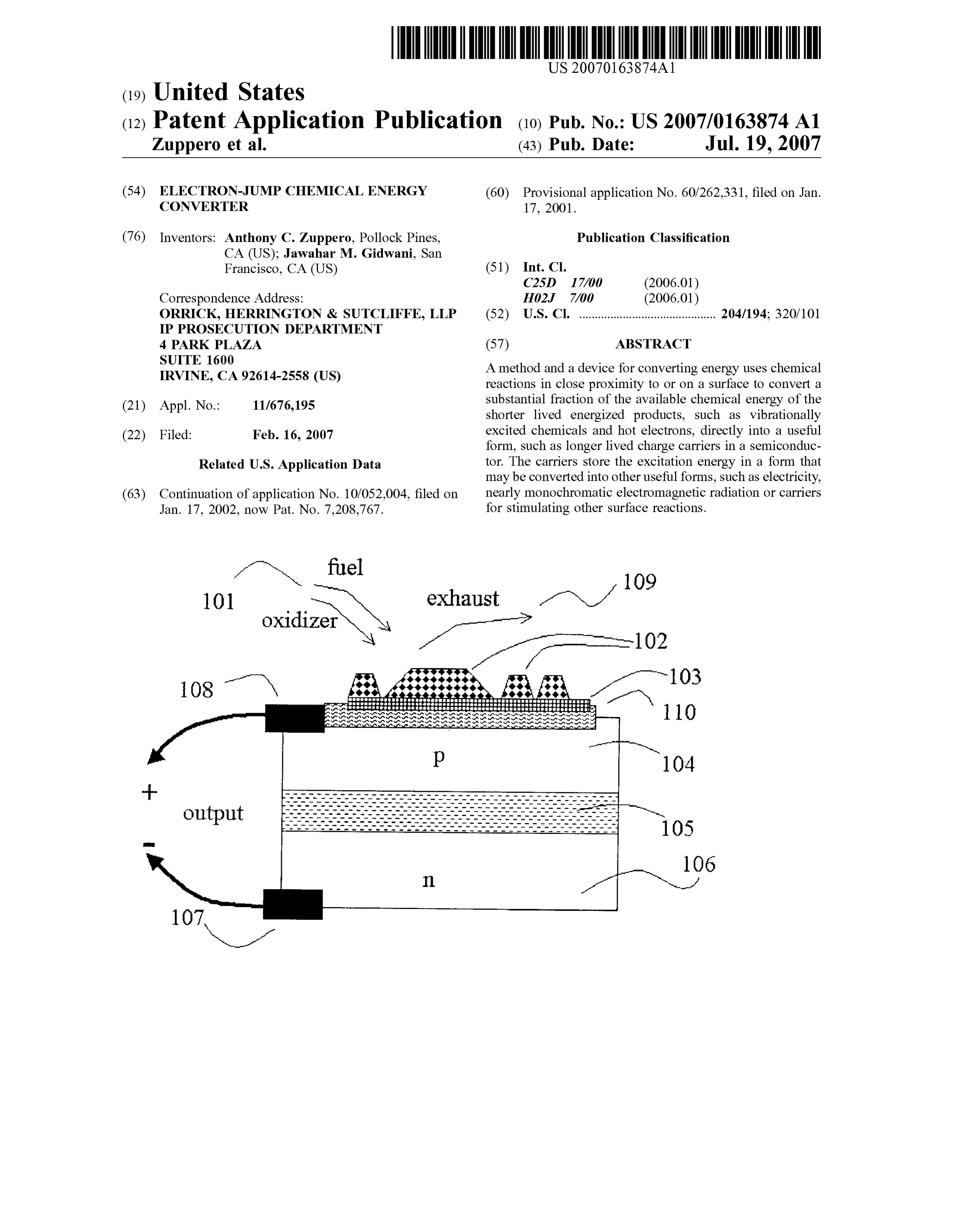
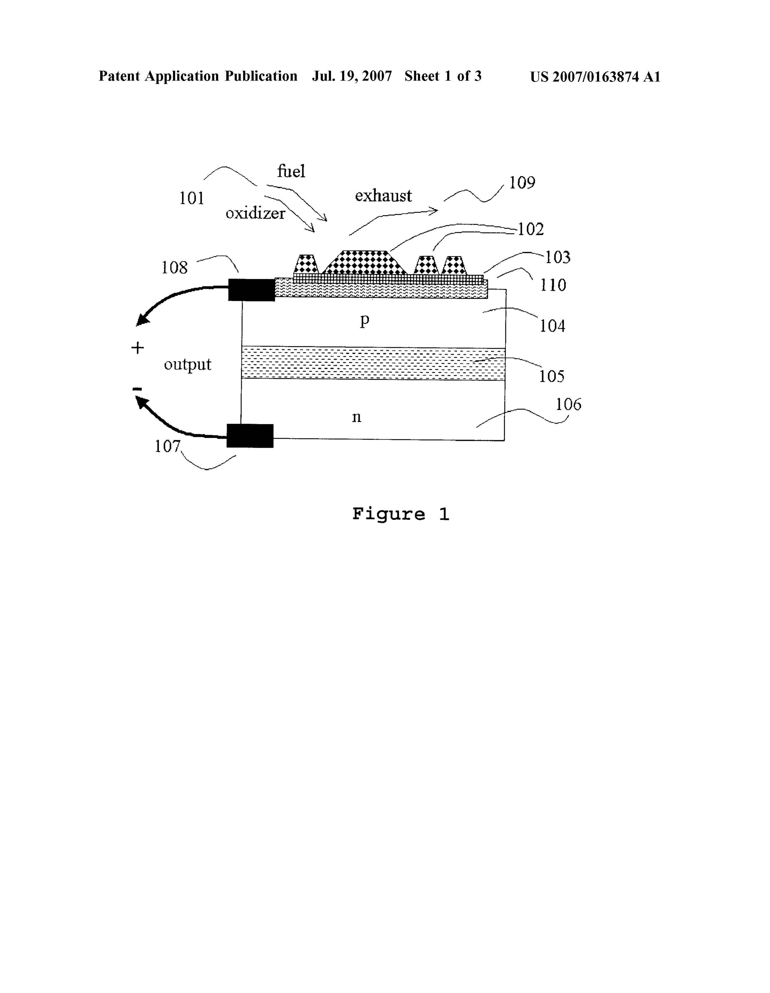
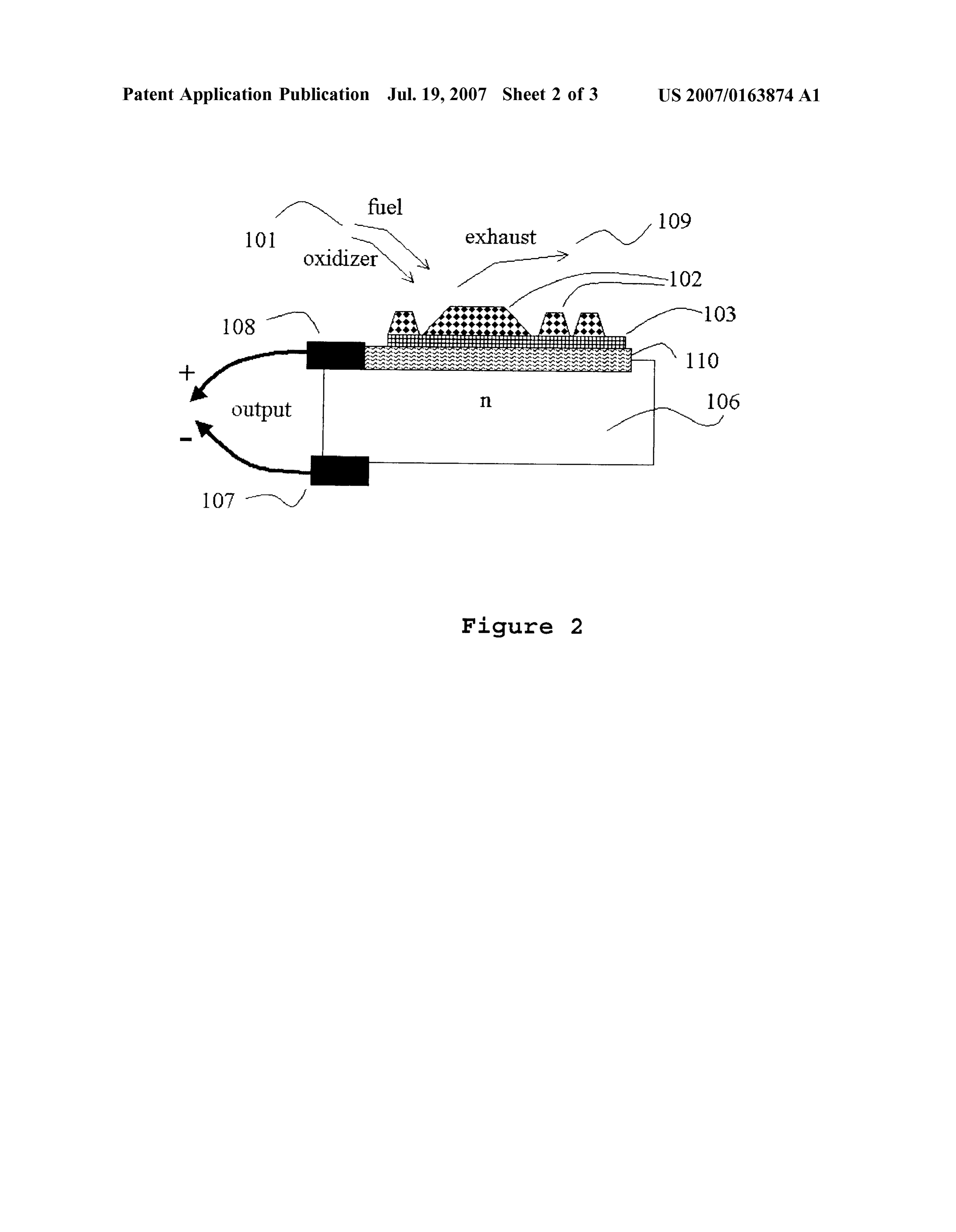
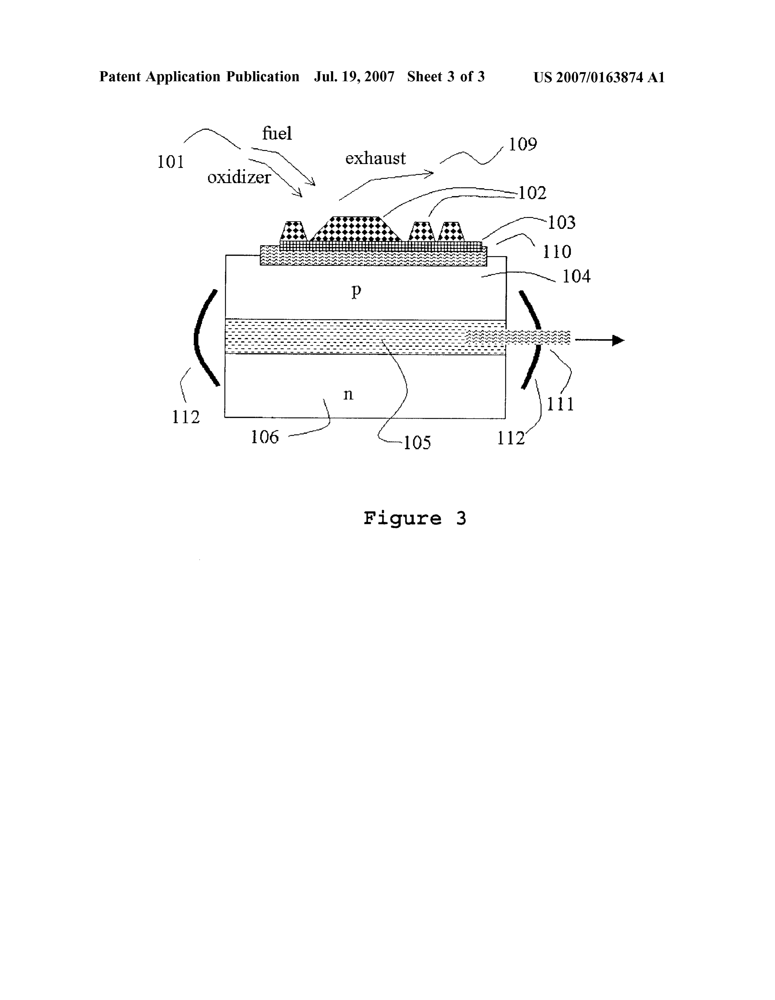
0025 The method includes forming the catalyst in any 0017 FIG. 1 shows a schematic cross section of an one of many different configurations, each configuration electric generator using the p-n junction; having particular features. The catalyst can be formed in any 0018 FIG. 2 shows a schematic cross section of an way including but not limited to clumps, monolayers, clus electric generator using the Schottky junction; and ters, ridges, step edges, quantum wells and quantum stadia. Configurations with edges and ridges may show the advan 0.019 FIG. 3 shows a schematic cross section of a laser tage of active sites for adsorption and reaction. Configura radiation Source using the p-n junction diode to generate a tions with monolayers may show the advantage of tailoring useful radiation from chemical reaction energies. and causing resonances and peaks in the density of States of electrons near the Fermi Surface, enhancing the transfer of
DETAILED DESCRIPTION OF THE energy at those energies. Clusters may show the advantage INVENTION of enhanced ballistic electron lifetimes and decoupling from Surface phonon states, increasing efficiency.
0020. The present invention is directed to converting a substantial fraction of the available chemical energy of 0026. The method for a continuous power generator in reactants into electrical or other forms of energy. In one one embodiment of the present invention includes choosing embodiment, chemical reactants are used to Supply the catalysts where the products of the reaction desorb and energy. In one embodiment, one or more catalysts are used rapidly leave the catalyst surface. The method also includes to form energized reaction products, or energized chemical choosing a catalyst or set of catalysts that readily react with products, in the near-field proximity to or on an energy the input reactants. Such catalysts have been known to those converter. Energy forms, also referred to as excitations, are skilled in the technological art, e.g., since the time (1800s)
Page 7
US 2007/0163874 A1 Jul. 19, 2007
when ethanol or methanol was observed reacting at a room from the energized chemical products directly into the temperature with air on wool or fine particle catalysts made energy converter. Such a method may include forming the of platinum or palladium. intervening path out of material with length short enough for 0027. The method and apparatus of the present invention ballistic charge carrier transport. in one embodiment injects or transfers the energetic charge 0034. The method and system of the present invention in carrier resulting from the interaction of a surface and the one embodiment creates the conditions on a reaction Surface energetically excited products into the semiconductor diode where the reaction paths strongly favor the generation of hot to create an excess of cited carriers in that diode. This excess carriers or excitations that can be converted directly into of excited carriers also creates a potential across the diode. useful potentials or excitations in a Substrate. According to Similarly, the method and apparatus of the present invention the methods of the present invention, such favorable con transfers or injects the energetic charge carriers into a ditions may be created, e.g., by tailoring the quantum states semiconductor or quantum well system. of the Surface by the use of quantum wells; choosing 0028. The method and system of the present invention in catalysts and Surface materials to favor energetic reactions; one embodiment efficiently collects and converts the result choosing reaction Surface geometries with an enhanced ing energy into electric power, for example using a forward concentration of the reaction sites favoring such excitations. biased semiconductor diode, or into an inverted population Reaction Surface geometries, e.g., may include steps and/or of excitations in a semiconductor or quantum well, which edge sites. The method of the present invention also may excitations can be converted into other useful forms of include choosing materials with Debye frequencies far from energy. the desired excitation frequencies. 0029. In one embodiment of the present invention, 0035) In one embodiment, the method includes forming chemical reactions may be used to generate the carriers the energy converter in contact with the reacting region. The instead of an applied Voltage. Chemical reactions may also term "contact includes configurations where catalysts, be used to power devices that would otherwise be powered materials, oxides or metals are placed between the energized by a source of electricity. For example, chemical reactions products and the energy converter and used as a path for the may also be used to power chips sets. Using chemical energy transfer. This includes placing the converter near the reactions to power chips sets permits the construction of reacting region, where “near” means within the distance that Volume, three dimensional computing systems, where the the excitation may either travel ballistically so that more energy source to power them is a flow fuel-oxidizer mixture. than 5% of the excitations retain more than 95% of its energy or where resonant tunneling may transport the energy Suf 0030. In one embodiment, the present invention uses and ficiently fast that the no more than 95% of the energy is lost. energizes a quantum well as the energy converter. An energy The figure "95% represents the attenuation effects of a converter of the present invention transforms a short-lived distance approximately 3 times the energy mean free path of carrier into a longer-lived carrier so that the carrier may be the charge carriers or electromagnetic coupling. The method used. Using a quantum well Substrate including a tunneling also includes placing the converter on, adjacent to or under barrier, a metal or semiconductor and another tunneling the reacting Surface. This includes Such configurations as barrier is a way to form the energy converter. This energy deep V channels and mesa structures. converter may be also formed in direct contact with the
Substrate, catalyst and reactants. The resonance levels 0036) This forming a path of material for ballistic charge formed by the quantum well provide temporary states to carrier transport includes limiting the path to a length less convert the ballistic carrier into a trapped, longer lived than approximately 4 times the energy mean free path of the excitation of the quantum well. One way the present inven charge carrier.
tion uses to extract the energy from the quantum well is 0037 Forming of the path includes forming part of the through stimulated emission of radiation. Another way the path from materials including any of metals, semiconductors present invention uses to extract the energy is through or insulators, and choosing materials with energy mean free generation of a potential. Yet another way is to power paths in excess of 1 atom layer.
nanodevices directly connected to the present invention.
0031. The current state of the art associated with quantum 0038. In one embodiment of the present invention, the well structures and semiconductors permits layers whose highly energetic relaxation of a reaction product created on dimensions are of the same order of magnitude as the energy the catalyst Surface transfers energy by injecting an electron mean free path of the ballistic carriers involved. or hole directly and ballistically into the catalyst surface. In this energy transfer process of the present invention, the 0032. The method and apparatus of the present invention vibrational excitation of the newly formed chemical specie may also distribute the longer lived carrier converted in a executes a resonant tunneling of its energy into the energy semiconductor Substrate to other locations on the reaction levels of the substrate. These energy levels include the very surface where the carrier leaves the semiconductor, converts broad band of available, unpopulated electron excitation back into a ballistic carrier in a catalyst or reaction Surface, states in either metals or semiconductor conduction bands. and performs useful work. Such work includes stimulating These energy levels include a similar band of hole states, reactions and energizing nano-mechanical devices or mol when the excitation transfer due to energized products is a ecules. Examples of Such nano-mechanical devices include hole.
a telescoping antenna, a nano-propeller, a C60 transistor, and the biological material kinesin. 0039 The emission of the electron or hot carrier in the present invention may utilize the inverse process of Des 0033. In one embodiment, the present invention includes orption by Electronic Transitions (DIET) or Desorption by a method to transfer energetic, or hot, electrons and holes Multiple Electronic Transitions (DIMET).
Page 8
US 2007/0163874 A1 Jul. 19, 2007
0040 Vibrationally excited anions (molecules or atoms lation inversion in those diodes and causes them to emit with an extra negative charge) absorb an electron and radiation. The method and apparatus of the present invention re-emit an electron into the lattice, carrying with it most of creates an identical forward bias using the hot carriers the excitation energy. By analogy, cations (positively generated at the reaction Surface and injected directly into charged) emit an electron and reabsorb it, emitting a hole the diode structure, instead of an external power Supply. A into the lattice, with the hole carrying the energy. The laser diode or a light emitting diode configuration may be electron or hole is the hot carrier. According to one embodi used in the present invention as an energy converter. An ment the present invention, the energy converter, Such as the example of a laser diode configuration is a Double-hetero semiconductor or the quantum well in immediate contact Structure.
with the substrate, converts the short-lived substrate hot 0045. In one embodiment, the present invention includes carrier into a longer-lived carrier or excitation in the semi a method of transferring reaction product excitations such as conductor or quantum well. the energy of a dipole active state or a vibrational state, 0041. The method includes using a thin electrode as part which are a type of excitation of the energized chemical of the reaction surface and substrate. The thickness of this products. The method includes enhancing resonant coupling electrode is preferably less than 3 times the energy mean free between the energized products and the energy converter path of the hot electrons or hot holes produced by the connected to the Substrate.
energized products. This electrode may also be made of 0046) This enhancing includes choosing operating biases catalyst metal, as an option. When the electrode is made that raise or lower the relative position of the energized from good conductor metals such as copper, aluminum, products with respect to the energy levels of the energy silver and gold the appropriate energy mean free path converter, so as to match those energy levels. For example, thickness may be substantially greater than in catalyst Such the energy levels of a semiconductor diode energy converter as platinum, palladium, iridium, rhodium, ruthenium, Vana include conduction band and Valence band edges. dia, titania, alumina, ruthenium oxide, oxides and other compounds. The thickness of materials forming the elec 0047. This enhancing includes forming a path between trode may typically range from 0.3 to 300 nanometers, products and energy converter where the length of a path is equivalent to approximately 1 to 1000 monolayers. The less than ten times the dimension of the evanescent electro thickness of materials forming the catalysts may typically magnetic field region of the energized products. range from 0.3 to 50 nanometers. 0048. In one embodiment, the dimension of the material 0042. The method includes forming electrodes that con between the reactants and the semiconductor Substrate is less tain oxides, insulators and mixed catalysts, including but not than the skin depth associated with the radiation transferring limited to platinum, palladium, iridium, rhodium, ruthe the energy. This embodiment is referred to as the “evanes nium, Vanadia, titania, alumina, ruthenium oxide, oxides and cent wave', where electromagnetic fields transfer the other compounds, whether or not these compounds are energy. In this embodiment of the present invention, instead catalysts, insulators or conductors. For example, the method of electron emissions and readsorption, the internal energy may include using ruthenium oxide, which is both an oxide of the energized reaction products is resonantly transferred and a conductor. to the carriers of the semiconductor or quantum well, through the intermediate materials such as the catalyst and 0043. In one embodiment of the present invention, the underlying Substrate.
catalyst surface is deliberately formed to favor hot carrier emission instead of substrate vibrations. The substrate vibra 0049. The method of the present invention includes tions are also known as phonons. The catalyst Surface may choosing a dimension between energized products and also be formed to preserve the energy of the hot carrier. The energy converter that is short enough not to dissipate the material of the reacting Surface may be chosen to have transferred energy. For example, the physical path from the phonon bands with energy much lower than the multi location of energized product on or near the reaction Surface quantum vibrational relaxation. A reacting Surface com to the electrode underlayer or energy converter, such as a posed of heavy atoms such as a palladium or platinum semiconductor diode, should preferably be less than 4 times catalyst exhibits such bands. Nearly all crystalline materials the energy mean free path of an electron (or hole) traveling have the desired phonon band frequencies. Further, the that path.
surface is formed to be so thin that the hot carrier, an electron 0050. The energy mean free path dimension is typically or hole, travels into the semiconductor Supporting the cata between 1 and approximately 300 monolayers for catalysts lyst before it looses very much of its energy. The dimension in the platinum group at room temperature, which is the associated with this ballistic transport is approximately a equivalent of approximately 0.3 and 100 nanometers. The small multiple of the energy mean free path of the hot carrier energy mean free path can be in excess of 115 nanometers in the catalysts or substrate. The “small multiple” means that in gold for electrons with energy less than 1 eV and is the thickness is thin enough so that the hot carrier or calculated to be in excess of approximately 150 nanometers excitation does not loose so much energy that the remaining in silver for 1 eV electrons.
energy is an impractically low value. Typically, the energy diminishes exponentially with characteristic dimension 0051. This forming the length of the ballistic transfer path “energy mean free path. A distance of '3' energy mean free includes fabricating a length through a conductor less than paths means that less than 5% of the carriers have approxi several times, e.g. four times, the energy mean free path of mately the same energy as when they started. the ballistic carrier.
0044) Applying an electrical forward bias across the 0052 The forming the length of the radiation path junction using external source of electricity creates a popu includes fabricating a path using materials with thickness
Page 9
US 2007/0163874 A1 Jul. 19, 2007
several times, e.g. 4 times, less than the penetration depth, product on or near the surface of the catalyst. It travels or the equivalent to the dimension of the near field region of through the catalyst and any intermediate material and enters the multipole radiator carrying the energy. the semiconductor Substrate. Once in the semiconductor, the 0053 Converting transferred excitations includes using hot carrier becomes a minority carrier. In one embodiment energy converters such as a semiconductor or a quantum of the present invention, the polarity and bandgap of the well, wherein short lived excitations such as hot carriers or semiconductor is deliberately chosen such that the hot energized product excitations are converted into longer lived carrier becomes a minority carrier when the hot carrier is in the semiconductor.
excitations such as carriers in the semiconductor or quantum well. 0062. In one embodiment, the semiconductor is chosen to 0054 The converting of excitations into useful forms be p-type when the hot carrier is an electron. The p-type includes conversion into an electrical potential, or into an semiconductor is physically connected to the catalyst so that inverted population of carriers suitable for stimulated emis any potential barrier between them is very small or nonex sion of radiation, or into an abundance of energetic carriers istent. The catalyst metal is placed on a thin electrode metal, that may themselves be used directly as energy sources. and the electrode material is bonded on the p-type semicon ductor. The barrier in a metal-metal contact is negligible.
0055. In one embodiment, the present invention also Highly doping the semiconductor, including the limit of high includes a method for forming the energy converter from a doping called degenerative doping, and selecting the elec semiconductor and converting the transferred excitations trode material from the ones known to be compatible with into excited carriers in the semiconductor. forming an electrical contact to the semiconductor reduces the barrier between electrode and semiconductor. The elec 0056. The method for forming the energy converter trode material may be another semiconductor, which is a includes choosing operating biases that raise or lower the method routinely used in the state of the art of semiconduc relative position of the energy levels of the semiconductor tor device fabrication. The result is that the catalyst Fermi diode. Such as conduction or Valence band edges so as to level and the Fermi level of the p-type semiconductor match those energy levels with those of the excited products. valence band (the top edge of the lower band) are equal. The 0057 The method may also include forming Schottky hot carrier energy is measured relative to that of the catalyst junction diodes. The method includes forming these junc Fermi level. The result is that the hot carrier approaches the tions with barrier potential high enough to permit useful semiconductor with an energy above that of the catalyst forward bias, which barrier is typically in excess of 0.05 Fermi level and therefore with approximately the same volt. The bandgap of the Schottky junction may be any energy above the Fermi level of the p-type semiconductor. useful value, including values much grater than the energy 0063. The hot carrier then tries to enter the semiconduc of the electron, or in excess of 1.5 volts. Varying the tor with an excess energy above that of the catalyst and semiconductor doping levels permits reducing the thickness semiconductor Valence band. By design, there are practically of the barrier. A thin barrier permits electron tunneling, no energy levels in the bandgap of the semiconductor for an which in turn permits forming an almost ohmic junction electron to excite. The only levels available in the semicon when doping approaches degenerate doping.
ductor are in the upper band, the conduction band. In one 0.058. The method includes choice of oxide layers, with embodiment of the present invention, the location of this thickness between 0.1 and 20 nanometers to form Schottky upper band is chosen to be slightly less than the energy of barriers and permits control of the barrier. Varying the the electron, so the electron can readily enter the semicon thickness of the oxide controls the carrier tunneling through ductor. This is achieved by forming the bandgap of the the oxide and hence the desired property of the junction. The semiconductor to be less than the energy of this hot electron, oxide may be placed anywhere between the energized prod or by choosing a semiconductor with the desired bandgap. ucts and the semiconductor. This means that the hot electron enters the p-type semicon 0059. The method may also include forming p-n junction ductor in its conduction band. This energizes the conduction diodes, and especially diodes where one or both polarities of band of the p-type semiconductor. The electron is thus the diode are heavily doped or degeneratively doped. The converted into a minority carrier instead of a ballistic carrier. method includes forming doping gradients, which may The minority carrier has a lifetime orders of magnitude broaden or narrow the junction region. longer than that of the ballistic carrier. 0060. It is recognized that the state of the are of con 0064. In one embodiment of the present invention, the structing p-n junction diodes includes many variants. Such semiconductor is chosen to be n-type when the hot carrier is variants include various regions and combinations of metals, a hole. The complimentary process as described with refer semiconductors, oxides and insulators outside of the diode.
ence to p-type semiconductor is performed, producing the
Some of these regions function to form ohmic or almost same result, i.e., the short-lived carrier into a longer-lived carrier.
ohmic contacts to the diode. Other functions include lattice matching. The diode may be formed with any variants of 0065 Advantageously, semiconductor materials with doping profile. All Such variants are functionally the same both indirect and direct bandgaps are available with energies diode: a p-n junction diode. from the lowest practical, of order 0.05 eV to higher than the 0061 The p-n junction energy converter of the present bond energies of most reactants, well in excess of 3 eV. invention converts a very short-lived hot carrier, which is a 0066. The lifetime of a minority carrier in a semiconduc ballistic electron or ballistic hole in the catalyst, into a much tor is typically at least 100 times longer than that of a longer-lived minority carrier in a semiconductor. For ballistic carrier. This longer lifetime gives the hot, minority example, a ballistic electron originates in the chemical carrier a chance to migrate, diffuse or be attracted by the
Page 10
US 2007/0163874 A1 Jul. 19, 2007
semiconductor internal field to a region in the semiconductor doping also permits use of relatively thin semiconductors, of opposite type, namely an n-type semiconductor. The p-n Such as semiconductors less than 1 micron thick. junction creates a strong electric field across it and attracts 0073 Calculations and models of an electric generator minority carriers approaching it.
using the above-described methods and using electron ener 0067. At the semiconductor junction, the minority carrier gies expected for electron jump reactions suggest that effi in the semiconductor finds exactly the same situation as it ciencies well in excess of 505 can be achieved with surface would find in a photovoltaic diode. As in a photovoltaic reaction power densities of order 10 watts per square cen diode, the electric field of the p-n junction sweeps the hot timeter. These values are consistent with existing and known carrier across the junction, forward biases the diode and catalysts and diodes.
generates a useful electrical potential. 0074 With the unique method of the present invention, a 0068. In one embodiment, the p-type semiconductor high output power is maintained because the products of the diode layer thickness is chosen to be smaller than the energy reaction desorb and leave the catalyst, making room for mean free path of the minority carriers transporting the more reactions of fuel and oxidizer at a rapid rate. energy. This mean free path is often referred to as the 0075) When the electron energy emitted by the energetic diffusion length. Over distances longer than the diffusion reactants is of order 1 volt, which exceeds thermal energy by length the carriers eventually recombine and generate heat. at least an order of magnitude, semiconductors with band 0069. The diode of the present invention in one embodi gaps in this range, of order 1 volt, such as silicon may be ment is similar to a photovoltaic diode, but different in a key, used. In one embodiment, a method of the present invention non-obvious way. A photovoltaic diode must be formed with uses such higher bandgap semiconductors and therefore ajunction region large enough to collect the light passing permits the apparatus of the present invention to be operated through it. This is typically much larger than a few hundred at a temperature above room temperature, e.g. above 100 nanometers. To increase the light collection distance, the Celsius. This expands the range of catalysts and semicon semiconductor junction must contain a relatively lower ductors that may be used and results in increased extractable doped region. This constraint forces the doping of one of the power per area.
nor p regions of the photovoltaic diode to be much less than 0076. The method includes using indirect bandgap semi what is considered to be heavy doping or degenerate doping. conductors such as silicon and germanium. Such materials This lower doping level reduces the resistance area product typically show a longer carrier lifetime than direct bandgap of the diode and reduces its efficiency. semiconductors. This tends to increase the efficiency of the 0070. In one embodiment, the diode of the present inven p-n junction embodiment.
tion does not need to collect Such photons and does not need 0077. The method includes using semiconductor com a large photon collection region. Therefore, the diode in the pounds whose bandgap can be tailored by the choice of present invention may use the highly doped or degenera allow composition. These include the InGaAsSb family of tively doped semiconductor for both polarities. This doping semiconductors, where the bandgap can range from approxi maximizes the resistance area product and therefore maxi mately 0.1 eV to above 1.5 eV depending on the ratio of In mizes the diode efficiency. Therefore, the diode of the to Ga and the ratio of AS to Sb. present invention can have both n and p regions that are highly or degeneratively doped. Unlike a photovoltaic diode, 0078. The method includes operating the diode with a high doping increases the collection efficiency of the diode bias to enhance resonant tunneling. One way to do this when of the present invention. electron transfer dominates is to operate the diode with a forward bias such that the conduction band of the semicon 0071 Also, unlike a photon-collecting photovoltaic ductor matches an energy level of the excited products. diode, the diode of the present invention has no constraint When hole transfer dominates, matching of the valence band that limits the minimum distance to the p-n junction or on is appropriate.
the thickness of the junction. This is advantageous since a high density of carriers in a heavily doped semiconductor 0079 The method includes using direct bandgap semi decreases the diffusion length of the minority carriers in the conductors such as those from the InGaAsSb family. Direct diode and decreasing the diffusion length is not the most bandgap semiconductors permit configurations that extract desired situation. Although this reduced diffusion length energy by stimulated emission of radiation. associated with the present invention may be of order 100 to 0080. In one embodiment, the present invention includes 500 nanometers, such reduction is acceptable in the present a method to enhance the peak power and the rate of energy invention because there is no constraint on the minimum distance to the p-n junction or on the thickness of the conversion by using the methods described above and junction. further including enhancing the desorption of exhaust prod ucts from the reaction region.
0072 This lack of a constraint may be highly advanta 0081. The method for this enhancing includes choosing geous. Accordingly, the semiconductor may be degenera catalysts with relatively low affinity for exhaust products. tively doped to a shallow depth, for example, 0.1 to 0.5 The enhancing includes choosing catalysts from those that microns (100 to 500 nanometers). Highly doped and degen are less selective with respect to reactants is an advantage. erative doped semiconductors may be used to minimize the Platinum, palladium and related catalysts have shown this distance from the catalyst and surface of the diode, where property with respect to hydrogen and alcohol combustion. the hot carriers are generated, to the p-n junction, where the forward bias is developed. Thus the high doping and small 0082 The method includes bringing fuel and oxidizer p-n junction dimensions become a useful method. The high into the region of reaction and permitting exhaust products
Page 11
US 2007/0163874 A1 Jul. 19, 2007
to leave the reaction region. Exhaust products may migrate junction 105. The internal electric field causes the carriers to and diffuse away. One way to do this includes flowing become majority carriers in the n-type semiconductor 106 of gaseous reactants over the reaction Surface and letting the the diode, causing the diode to become forward biased. exhaust products leave the Surface into the gas flow. 0089 Electricity is generated by reason of the forward 0.083 Quantum wells offer the possibility of creating bias developed across the diode and is extracted as a forward resonances to capture the reactant excitations. According to current between the positive electrode 108 and the negative the state of the art, external electric currents energize quan electrode 107.
tum wells and dots formed into near ideal 4 level lasers.
According to the present invention, the same kinds of wells 0090 FIG. 2 shows a cross section of the apparatus of the and dots may be energized directly from the energy of present invention in one embodiment for the case where electrons are the created as the result of reactions and where reactantS.
a Schottkyjunction diode converts the electrons into useful 0084. In one embodiment, an apparatus of the present forms of energy such as electricity. As in FIG. 1, fuel and invention includes a reaction region and Surface with a oxidizer reactants 101 flow into the reaction region 102 and catalyst and upon which reactants form energized specie and 103 and exhaust products 109 leave the reaction region. emit charge carriers. An energy converter is placed within a Reactions occur on the catalyst structures 102, shown as distance less than 10 times the energy mean free path of layers or clusters, and may occur on the substrate 103 as in excitations carrying the energy to an energy converter. An the previous embodiment.
energy converter in the apparatus includes a semiconductor 0091. The substrate 110 is a metal chosen to form a p-n junction. Schottky barrier at the metal-semiconductor junction. The 0085 FIG. 1 shows a cross section of an apparatus in one metal substrate 110 therefore also forms the electrical con embodiment of the present invention for the case where hot, nection to the diode, also referred to as the diode electrode. energetic electrons are the form of energy created as the 0092. Some of the hot electrons created on the reaction result of reactions and where a p-n junction diode converts surface and region 102 and 103 have energy greater than the the electrons into useful forms of energy Such as electricity. Schottky barrier between the diode electrode 110 and semi Fuel and oxidizer reactants 101 flow into the reaction region conductor 106. These electrons travel ballistically over this including catalyst 102 and substrate 103, and exhaust prod barrier and enter the n-type semiconductor 106 where they ucts 109 leave the reaction region. become majority carriers in the semiconductor. 0.086 Reactions occur on the surface of the catalysts 102 0093 Collisions with the lattice and electrons in the and substrate 103. Catalyst structures 102 are shown as semiconductor degrade the excess energy to a value Sub layers or clusters formed on the substrate 103. The substrate stantially less than the barrier. The result of this energy loss 103 may contain materials such as catalyst materials, oxides, is to diminish the number of electrons that travel in the non-conductors and alloys including catalyst material and is reverse direction. This permits a forward bias on the diode a part of the reaction region. A thin substrate 110 physically to develop.
connects the reaction region including catalysts 102 and 0094 Electricity is generated by reason of the forward substrate 103 to the diode p-type semiconductor element bias generated as a result of the hot electron transfer across
the diode metal semiconductor junction and is extracted as 0087 Substrates 103 and 110 are shown separately to a forward current between the positive electrode 108 and the illustrate that material constraints may force the need for one negative electrode 107.
type of material forming a substrate on which to form 0095. In one embodiment, a method to collect the energy catalyst structures and reaction Surfaces, and for another of Surface reactions includes using a diode similar to that type of material to form an ohmic or almost ohmic connec used in ballistic electron generation and detection, e.g., a tion to the semiconductor. When materials are compatible, Schottky diode. In this embodiment, a catalyst and reactant either substrate may be formed from the semiconductor flow similar to that used in the p-n junction diode device itself, or either substrate may be formed form the catalyst may also be used. The thin catalyst is Supported on a itself, or combinations thereof. For example, when the substrate formed by a thin electrode of a Schottky diode. The semiconductor is very heavily doped, which is also referred thin electrode may also be formed from the same materials to as degeneratively doped, then the catalyst metal may form as the catalysts.
an ohmic junction or an almost ohmic junction to the semiconductor. In this case, the catalyst may act as the 0096. In one embodiment of the present invention, a Substrate 110 to connect the reaction region to the semicon Schottky junction typically includes a metal deposited on a ductor. Further, as another example, if the catalyst forms the doped semiconductor. A Schottky junction to capture hot desired structures directly on the semiconductor, then the electrons in the present invention may be made by bonding catalyst itself may form its own substrate 103. a metal, including catalyst metals such as platinum, directly 0088. The hot electrons created on the reaction surface to the Surface of an n-type silicon semiconductor. A voltage 102 and 103 travel through the thin substrate 110 and into barrier develops within approximately several atomic mono the p-type semiconductor 104 where the electrons are con layers of the metal-semiconductor junction, between the verted into minority carriers in the semiconductor. Charge metal and the semiconductor, with value typically between 0.4 and 0.9 electron volts.
balance occurs by the transfer of a hole from the p-type semiconductor into the reaction region. The minority carri 0097. A ballistic electron generated in the diode metal ers travel to the p-n junction 105 of the diode both by electrode may directly pass into the semiconductor if its diffusion and by reason of the internal electric field of the energy is greater than the Schottky barrier. That is, if the
Page 12
US 2007/0163874 A1 Jul. 19, 2007
electron has greater than about 0.4 to 0.9 eV above the 0.104) The method of the present invention may also catalyst Fermi level, it will ballistically travel directly over include converting charge carrier energy into difference in the Schottky barrier. The hot electron then collides with Fermi level, also known as chemical potential, across a other electrons or atoms in the semiconductor. Within the diode junction. The diode may a Schottky junction diode and length equal to a few times its energy mean free path in the also may be formed from a bipolar semiconductor material semiconductor the hot electron becomes just a thermal, such as InGaAsSb. InGaAsSb ratio may be tailored to majority carrier electron. Its energy is now far below the provide a bandgap that matches energy transitions of excited Schottky barrier and it cannot travel back into the metal. products.
This causes a forward bias on the diode. The result is the conversion of hot electron energy into a measurable current 0105 The diode in the present invention used to collect through the diode and may result in a measurable Voltage electrons may be formed using an n-type semiconductor. across the diode. The diode in the present invention used to collect holes may be formed using a p-type semiconductor. The diode may be 0098. The ballistic electron may travel into the diode if it formed with low barrier, e.g., by doping the semiconductor does not decay first. The ballistic electron will not decay if highly or degeneratively to reduce the barrier. The semicon the energy mean free path in the catalyst and diode electrode ductor may also be doped in excess of 1E18 per cubic metal is longer than the distance the electron has to go to get centimeter.
into the diode. This dimension is typically of order 100 0106 The diode in the present invention may be formed nanometers, or 300 monolayers, or less. An advantage of with an oxide barrier between the catalyst and the diode. The using a Schottkyjunction energy converter is the simplicity barrier may be placed between the electrode of the diode and of the device.
the semiconductor of the diode. The barrier may also be 0099 FIG.3 shows a cross section of the apparatus in one placed between the catalyst and the semiconductor of the embodiment of the present invention where electrons are diode. The barrier may also be placed between the energized created as a result of reactions and result in a population products and the diode.
inversion of carriers in the diode junction region. Stimulated 0.107 The barrier thickness may be fonmed to be less emission of radiation with photon energy approximately than the ballistic transport dimension for the charge carrier equal to that of the bandgap removes energy from the system that forward biases the diode. The barrier thickness may be, in the form of electromagnetic radiation, including coherent e.g., less than 100 nanometers.
radiation.
0100. In one embodiment, the chemical reactions inject 0108. In the present invention, the diode may be forward hot electrons into the p-n junction diode in a similar manner biased so that its conduction band matches a desired energy described with reference to FIG. 1. The diode becomes level of the excited state products. The diode may be forward biased. The electrons and holes are allowed to operated with a forward bias in excess of 0.05 volts. The accumulate instead of being used as an electrical energy diode may be formed so that its conduction band matches a Source. The result is a population inversion of electrons and desired energy level of the excited state products. holes. The electrons and holes recombine, emitting photons 0.109 As described above, the diode may be a p-n junc with energy approximately equal to the bandgap. tion diode. The p-n junction diode that collects electrons is 0101 Tailoring junction region of a diode by doping p formed such that a first electrode of the diode, which is in and n regions promotes flooding of the junction with both contact with the reacting Surface, is in contact with a p-type electrons and holes. The junction region thereby acquires an semiconductor. An n-type semiconductor is formed adjacent inverted population. Choosing a semiconductor to be a to the p-type semiconductor, forming the p-n junction, and the second electrode of the diode is in contact with the direct bandgap material promotes photon radiation over n-type semiconductor.
phonon emission.
0102) An optical cavity 112 provides the means to extract 0110. The p-n junction diode that collects holes is formed the energy in the form of coherent radiation 111 by means of such that a first electrode of the diode, which is in contact stimulated emission. The optical cavity shown in FIG. 3 is with the reacting Surface, is in contact with a n-type semi shown as an example only. Other optical cavities may also conductor. A p-type semiconductor is formed adjacent to the be employed. Those skilled in the technological art will n-type semiconductor, forming the p-n junction, and the appreciate that there are many known ways to couple an second electrode of the diode is in contact with the p-type semiconductor.
energized semiconductor system to an optical cavity to produce radiation and coherent radiation output. 0111. The p-n junction diode may be formed from a 0103 As described above, the method for generating semiconductor with bandgap matching a desired energy electricity in the present invention includes using reactants level transition of the energized products on the surface of to Supply the energy; using one or more catalysts to form the catalyst. The p-n junction diode may also be formed with energized chemical products in the near-field proximity to or a low Schottky barrier between an electrode and the semi on an energy converter, using the energy converter to collect conductor. The barrier may be formed to be less than 0.4 eV. and transfer energy forms, also called excitations, which are The semiconductor in the p-n junction diode may be doped emitted by the energized reaction products. The method may highly or degeneratively to reduce the barrier. For example, also include forming the catalysts, interconnections and the semiconductor may be doped in excess of 1E18 per cubic Substrates such that the distance from the reacting chemicals centimeter. The p-n junction may be formed from a bipolar to the energy converter is less than approximately 4 times semiconductor or from a direct bandgap semiconductor. the various energy mean free paths of the forms of energy 0.112. The p-n junction diode may be forward biased so going into the energy converter. that its conduction band matches a desired energy level of
Page 13
US 2007/0163874 A1 Jul. 19, 2007
the excited State products. The p-n junction diode may be layers, islands, pancakes and quantum dots, where the formed with a bandgap in excess of 0.04 volts. structures contain less than 200 atoms and/or where the 0113. The method of the present invention also includes structures contain less than 300 monatomic layers. The forming the connection between energized products and catalyst structures may be formed into atomically smooth semiconductor to create for an energetic electron or hole Superlattices. The catalyst structures may also be formed formed outside the semiconductor a ballistic or tunneling with dimensions less than 10 monolayers, e.g., where the path into the conduction band of semiconductor for an structures contain less than 200 atoms. The catalyst may, electron and the valence band for hole. e.g., formed from gold, silver, copper and nickel. 0114. The connection may be formed with a vacuum path 0.121. An electrode interlayer may be formed to connect dimension less than 20 nanometers and a material path less the catalyst to semiconductor to provide an electrical con than 100 nanometers between energized products and semi nection to semiconductor. The interlayer thickness may be conductor. formed to be less than mean free path of the charge carriers causing forward bias of the diode, e.g., a thickness less than 0115) In the present invention, the catalyst structures may 200 nanometers. Metals compatible with forming an elec be formed into quantum well structures. Such as layers, trode with the semiconductor may be used to form the islands, pancakes and quantum dots, where e.g., the struc interlayers. Examples of these metals include Mg, Sb, Al, tures may contain less than 200 atoms. The catalyst struc Ag, Sn, Cu or Ni. The interlayer may also be formed from tures may also be formed into atomically Smooth Superlat metals that match the lattice parameter of the catalyst to the tices. The catalyst structures may be formed with interlayer.
dimensions less than 10 monolayers, e.g., where the mono layers contain less than 200 atoms. The catalysts may be 0.122 The present invention also includes an apparatus formed, e.g., from gold, silver, copper, or nickel. for generating electricity. The apparatus includes a reactant flow system where reactants enter and exhaust products 0116. The energy converter in the present invention may leave the vicinity of the reaction Surface; a reaction Surface be formed by various combinations of metal-semiconductor containing a catalyst and upon which reactants may form oxide structures. An electrode interlayer connecting catalyst energized specie in close proximity to an energy converter to semiconductor may be formed to provide an electrical connected to the Surface; and an energy converter Such as a connection to semiconductor. The interlayer thickness may semiconductor. For example, as described above, the energy be less than the mean free path of the charge carriers causing converter may be a Schottky diode. Alternatively, the energy forward bias of the diode, e.g., less than 200 nanometers. converter is a p-n junction diode. The interlayer may be formed from metals compatible with forming an electrode to the semiconductor. Examples of 0123 The present invention also includes an apparatus such metals include Mg, Sb, Al, Ag, Sn, Cu or Ni. The for generating coherent radiation. The apparatus includes a interlayer may be formed from metals that match the lattice reactant flow system where reactants enter and exhaust parameter of the catalyst to the interlayer. As described products leave the vicinity of the reaction Surface; a reaction above, the method of the present invention may include Surface containing a catalyst and upon which reactants may mixing fuel and air in the channel providing reactants to the form energized specie in close proximity to an energy catalyst Surface. converter connected to the Surface; and energy converter attached to a reaction Surface including a p-n junction 0117. In one embodiment, the energy converter of the semiconductor. In one embodiment, the p-n junction diode is present invention is placed next to, below or under the coupled to an optical cavity.
catalyst. Charge carrier motion is converted into an inverted population of carriers in a p-n junction diode and the energy 0.124 While the invention has been particularly shown stored in the carriers is extracted using stimulated emission. and described with respect to particular embodiments thereof, it will be understood by those skilled in the art that 0118. In one embodiment, the diode in the present inven the foregoing and other changes in form and details may be tion is formed from direct bandgap semiconductors. The made therein without departing from the spirit and scope of diode may be coupled to the on optical cavity. The diode is the invention.
formed from a semiconductor with bandgap matching a desired energy level transition of the energized products on 1. A method for converting chemical energy into a useful the surface of the catalyst. The p-n junction diode may be form comprising:
formed with a low Schottky barrier between an electrode and the semiconductor such that the barrier is less than 0.4 using reactants and catalyst to create highly vibrationally eV. The barrier may be reduced by doping the semiconductor excited molecules, the highly vibrationally excited highly or degeneratively, e.g., doping the semiconductor in molecules being created in a catalytic reaction where at excess of 1E18 per cubic centimeter. least some of products of the catalytic reaction desorb and leave a Surface of the catalytic reaction;
0119) A connection may be formed between energized products and diode having a ballistic or tunneling path for an coupling the highly vibrationally excited molecules with energetic electron or hole formed outside the semiconductor electrons by placing the highly vibrationally excited to force itself into the conduction band of semiconductor for molecules near a conducting Surface for electron-jump an electron and the valence band for hole. The connection effect to occur;
may be formed with a vacuum path dimension less than 20 causing at least some of vibrational energy of the highly nanometers and an material path less than 100 nanometers. vibrationally excited molecules to transfer to the elec 0120) The energy converter in this embodiment may trons of the conducting Surface, resulting in excited include structures into quantum well structures, such as carriers being created;
Page 14
US 2007/0163874 A1 Jul. 19, 2007
collecting the excited carriers; and where at least some of products of the catalytic reaction converting energy of the excited carriers into electrical desorb and leave a Surface of the catalytic reaction; energy. coupling the highly vibrationally excited molecules with 2. The method of claim 1, wherein the collecting includes electrons by placing the highly vibrationally excited collecting the excited carriers using a semiconductor. molecules near a conducting Surface for electron-jump 3. The method of claim 1, wherein the converting includes effect to occur;
converting the excited carriers into chemical potential across causing at least some of vibrational energy of the highly a diode junction to generate electrical energy. vibrationally excited molecules to transfer to the elec 4. The method of claim 1, wherein the using reactants trons of the conducting Surface, resulting in excited includes reacting fuel with oxidizer. carriers being created;
5. The method of claim 1, wherein the using reactants includes allowing reactants to enter and exhaust products to collecting the excited carriers; and leave a vicinity of the conducting Surface where reactions converting an energy of the excited carriers into electric that create the highly vibrationally excited molecules occur. ity.
6. The method of claim 1, wherein the collecting includes 17. The method of claim 16, wherein the reactants include collecting the excited carriers using a semiconductor diode. a fuel.
7. The method of claim 1, wherein the collecting includes 18. The method of claim 16, wherein the reactants include collecting the excited carriers using a Schottky junction an oxidizer.
diode.
8. The method of claim 1, wherein the collecting includes 19. The method of claim 16, wherein the one or more collecting the excited carriers using a bipolar semiconductor. catalyst Surfaces include one or more step formations. 9. The method of claim 1, wherein the collecting includes 20. The method of claim 16, wherein the one or more collecting the excited carriers using an n-type semiconduc reactants include at least HO and the catalyst includes at tOr. least Ag.
10. The method of claim 1, wherein the collecting 21. A method for an electric generator that converts includes collecting the excited carriers using a p-type semi chemical energy into electricity, comprising: conductor diode. using reactants and catalyst to create highly vibrationally 11. The method of claim 1, wherein the collecting excited molecules, the highly vibrationally excited includes collecting the excited carriers using a p-n junction molecules being created in a catalytic reaction where at diode. least some of products of the catalytic reaction desorb 12. The method of claim 1, further including placing a and leave a Surface of the catalytic reaction; first electrode in contact with the conducting Surface. coupling the highly vibrationally excited molecules with 13. The method of claim 1, wherein the reactants include electrons by placing the highly vibrationally excited a fuel.
14. The method of claim 1, wherein the reactants include molecules near a conducting Surface for electron-jump an oxidizer. effect to occur;
15. The method of claim 1, wherein the one or more causing at least some of vibrational energy of the highly reactants include at least H2O and the catalyst includes at vibrationally excited molecules to transfer to the elec least Ag. trons of the conducting Surface, resulting in excited 16. A method for generating a useful form of energy, carriers being created:
comprising:
collecting the excited carriers; and using one or more reactants on one or more catalyst converting energy of the excited carriers into electrical Surfaces to create highly energy.
vibrationally excited molecules, the highly vibrationally excited molecules being created in a catalytic reaction
Provenance
- Collection
- Patents citing this work
- Original assignee
- Neokismet LLC
- Pages
- 14
- Method
- pdftotext (the PDF's own text layer) + pdftoppm 300dpi page scans
- Patent office record
- patents.google.com →
- Source
- Google Patents citing-documents table
- Inventors
- Anthony Zuppero; Jawahar Gidwani; Neokismet LLC
- Published
- 2007-07-19
- Transcribed from
- patentimages.storage.googleapis.com →