patent · US5470395
Reversible thermoelectric converter
28 November 1995
Page 1 — bibliographic record
United States Patent (19) 11 Patent Number: 5,470,395 Yater et al. 45 Date of Patent: Nov. 28, 1995
54 REVERSIBLE THERMOELECTRIC 4,710,588 12/1987 Ellion ...................................... 1361206 CONVERTER 4,795,498 if 1989 Germanton et al. .................... 136,225 76 Inventors: Joseph C. Yater, 71 Autumn La., FOREIGN PATENT DOC NTS Lincoln, Mass. 01773; Jane A. Yater, 0369670 5/1990 European Pat. Off..
2H Sutton Dr., Matawan, N.J. 07747;
Joan E. Yater, 7205 Hart La. #3018, OTHER PUBLICATIONS
Austin, Tex. 78731 Patent Abstracts of Japan, vol. 14, No. 362, (E-0960) 6 Aug.
21 Appl. No.: 269,654 E. A. DeMeo et al, Proc. of the 21st Inst. of Elect. & Electronics Engineers Photovoltiac Specialists Conference, 22 Filled: Jun. 30, 1994 1990, Kissimmee, May 21-25, 1990 (Inst, of Elect. & Electronics Eng.), New York, 1990 pp. 16–23, “Solar Pho
Related U.S. Application Data tovoltaic Power: A U.S. Electric Utility R&D Perspective'. J. C. Yater, Physical Review A, vol. 20, No. 2, Aug. 1979, 62 Eof Ser. No. 860,677, Mar. 30, 1992, Pat. No. pp. 623-627, "Rebuttal to Comments on "Power Conversion eval W. of Energy Fluctuations'.
(51] Int. Cl. ......................................... HOL 35/28 a- ad 52 U.S. Cl. .......................... 136/203; 136/204; 136/205; (List continued on next page.)
s Primary Examiner-Donald P. Walsh 58 Field of Search ..................................... 136/200, 203, Assistant Examiner-Chrisman D. Carroll 136/204, 224, 225, 205, 208; 62/3.2, 3.3, Attorney, Agent, or Firm-Wolf, Greenfield & Sacks 35, 3.7; 250/338.3 y y
A reversible thermoelectric converter includes first and
3,116,427 12/1963 Giaever .................................. 307/88.5 between the first and second quantum well diodes without a 3,126,509 3/1964 Pulvari ...................................... 323/74 thermal barrier between them. Each quantum well diode 3.243,687 3/1966 Hoh ............................................. 322/2 includes first and second electrodes wherein electrons are 3,259,759 7/1966 Giaever ...... 307/88.5 quantized in discrete energy levels and a dielectric layer 3,272,986 9/966 Schmidt .................................... 250/86 providing a potential barrier between the first and second 3,356,864 12/1967 Giaever ...... ... 307/88.5 electrodes. When electrons in the first quantum well diode 3,419,767 12/1968 Dahlberg ................................. 37,235 have a higher temperature than the electrons in the second 3,460,008 8/1969 Dahlberg ... 37,235 quantum well diode, electric voltage fluctuations resulting 3,495,141 2/1970 Dahlberg.... 317/235 from transitions of the electrons between the energy levels 3,60,632 8/1971 Frazier ....... 307/219 3,631,306 12/1971 Hitchcock .. 317,234 in the first quantum well diode are coupled from the first 3,751,687 8/1973 Jutzi ........... ... 307/279 quantum well diode to the second quantum well diode. The 3,890,161 6/1975 Brown, III . . . 136/212 reversible thermoelectric converter can be operated for 3,920,413 11/1975 Lowery ...... ... 29797 power conversion of thermal energy to electric energy, as a 4,004,210 1/1977 Yater ...... 322?2 R heat pump or a refrigerator, or as an amplifier. A planar array 4,019,113 4/1977 Hartman ................................... 321/15 of reversible thermoelectric converter elements provides a 4,106,952 8/978 Kravitz. ....... 136789 HY desired output voltage and current. 4,467,611 8/1984 Nelson et al. ................................ 62/3 4,631,350 12/1986 Germanton et al. .................... 1361225 4,663,115 5/1987 Russell .................................... 376/320 21 Claims, 12 Drawing Sheets
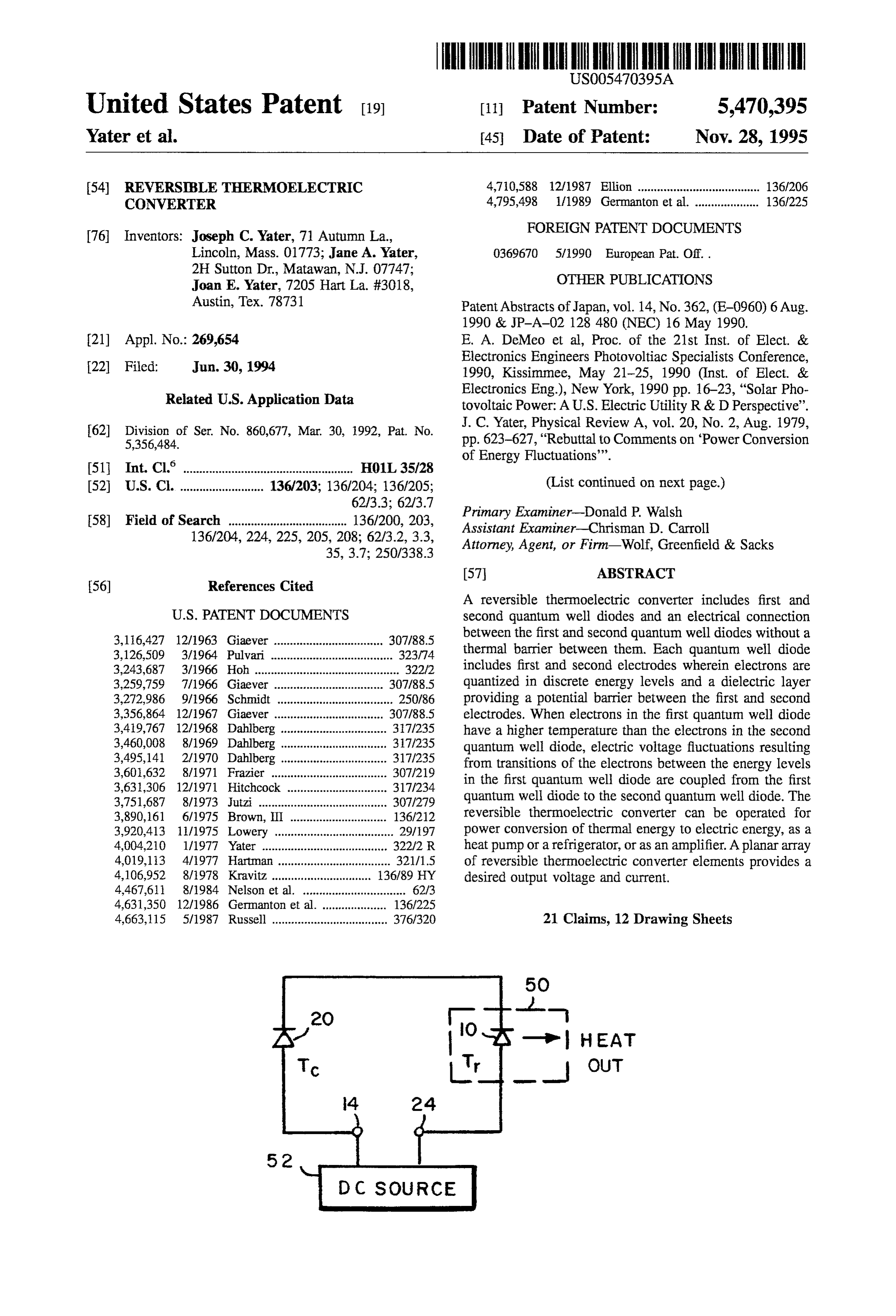
DC SOURCE
Page 2
OTHER PUBLICATIONS R. Dingle, "Confined Carrier Quantum States in Ultrathin Semi-Conductor Heterostructures", Festkorperprobleme
J. C. Yater, Physical Review A, vol. 26, No. 1, Jul. 1982, pp. XV, 1975, pp. 21-26.
522–538, "Physical Basis of Power Conversion of Energy
Fluctuations'. H. Nanto et al., "Electrical & Optical Prop. of Indium Tin J. C. Yater, Solar Cells, vol. 10, Aug. 1983, pp. 237-255, Oxide Thin Films...", J. Appl. Phys. vol. 63, No. 8, 15 Apr. "Physical Basis of Power Conversion of Energy Fluctua 1988, pp. 2711-2716.
tions of Hot Electrons'. J. C. Yater, "Power Conversion of Energy Fluctuations', R. C. Jaklevic et al., Physical Review B, vol. 12, No. 10, Physical Rev. A., vol. 10, No. 4, Oct. 1974, pp. 1361-1369. Nov. 15, 1975, pp. 4146-4160, “Experimental Study of J. C. Yater, "Relation of the Second Law of Thermodynam Quantum Size Effects in Thin Metal Films by Electron ics... ', Physical Review A, vol. 20, No. 4, Oct. 1979, pp. Tunneling'. 1614-1618.
F. Capasso et al, "Quantum Electron Devices', Physics J. C. Yater, "Particle Interactions in the Power Conversion of Today, Feb. 1990, pp. 74-82. Energy Fluctuations', Physical Review A, vol. 26, No. 2, R. Eisberg & R. Resnick, Quant. Phys. of Atoms, Molecules, Nov. 1982, pp. 2954-2967.
Solids, Nuclei & Part., J. Wiley & Sons, Inc., New York 1974, pp. 442-444. J. C. Yater, "Solar Reversible Energy Fluctuation Con W. Band, An Introduction To Quantum Statistics, D. Van verter', SPIE Proceedings, vol. 407, Apr. 1983. Nostrand Co., Inc., New York, 1955, pp. 38–40. "Converting Solar Energy Into Electricity: A Major Break J. C. Yater, Applied Optics, Feb. 1975, pp. 526-536, "Space through?' House of Representatives, Jun. 11, 1976, pp. Reflectors for Radar and Astronomy'. 1-38.
Page 3
Drawing sheet — no readable text.
Page 4
Drawing sheet — no readable text.
Page 5
Drawing sheet — no readable text.
Page 6
Drawing sheet — no readable text.
Page 7
Drawing sheet — no readable text.
Page 8
Drawing sheet — no readable text.
Page 9
Drawing sheet — no readable text.
Page 10
Drawing sheet — no readable text.
Page 11
Drawing sheet — no readable text.
Page 12
Drawing sheet — no readable text.
Page 13
Drawing sheet — no readable text.
Page 14
Drawing sheet — no readable text.
Page 15
REVERSIBLE THERMOELECTRIC electric converters known to applicants include a separate CONVERTER thermal barrier between the hot and cold layers of the circuit. Quantum size effects in thin metal films is described by R.
This application is a division of application Ser. No. C. Jaklevicetal in Physical Review B, Vol. 12, No. 10, Nov. 07/860,677 filed Mar. 30, 1992, now U.S. Pat. No. 5,356, 5 15, 1975, pages 4146-4160. Devices involving quantum 484. effects are described by F. Capasso et al in "Quantum Electron Devices", Physics Today, February 1990, pages
FIELD OF THE INVENTION 74-82. A typical quantum well diode includes a thin dielec tric layer between two thin metal layers. Electrons in the
This invention relates to reversible thermoelectric power 10 metal layers are quantized into discrete energy levels in a conversion devices, and more particularly, to reversible direction perpendicular to the metal surface. The dielectric thermoelectric converters which utilize quantum well layer forms a potential barrier.
diodes. More specifically, the invention relates to devices for It is a general object of the present invention to provide converting the thermal energy of hot electrons to electric improved reversible thermoelectric converters. energy and for pumping heat from low temperature regions 15 to high temperature regions, and to applications of such It is another object of the present invention to provide an devices. improved reversible thermoelectric converter including a thin film quantum well diode for directly converting thermal
BACKGROUND OF THE INVENTION energy of hot electrons to electric energy.
20 It is a further object of the present invention to provide
Devices for converting thermal directly to electric energy reversible thermoelectric converters with improved effi have been extensively investigated. The most commonly ciency of conversion of solar energy to electrical energy. utilized devices have been thermionic converters working It is yet another object of the present invention to provide from high temperature sources and silicon cells utilizing the hot electrons for the reversible thermoelectric converter input thermal energy of solar radiation. Such devices have 25 from different heat sources including fossil, nuclear and limited operating temperature ranges. In addition, the effi geothermal heat sources.
ciencies for the direct conversion of solar energy to elec It is a further object of the present invention to provide tricity that are required to be competitive with convention ally generated electricity in many U.S. markets over the next efficient operation of the reversible thermoelectric converter few decades have not yet been achieved. These required 30 at low temperatures.
efficiencies range from the lowest efficiency requirement of 10% module efficiency for flat plate modules to the highest SUMMARY OF THE INVENTION efficiency requirement of 25% module efficiency for con centrated solar energy. These required efficiencies are According to the present invention, these and other reported by E. A. DeMeo et al in Proceedings of the 21st 35 objects and advantages are achieved in a reversible thermo Institute of Electrical and Electronics Engineers Photovol electric converter comprising a first device, or element, and taic Specialists Conference-1990, Kissimmee, May 21-25, a second device, or element. The first and second devices are 1990 (Institute of Electrical and Electronics Engineers, New electrically connected together without a thermal barrier York, 1990), pp. 16-23. between them. The first and second devices each comprise A reversible thermoelectric converter having a high oper 40 first and Second regions wherein electric carriers are quan ating efficiency is disclosed in U.S. Pat. No. 4,004,210 tized in discrete energy levels, and a third region that issued Jan. 18, 1977 to Yater. The disclosed device com provides a potential barrier between the first and second prises a first layer of microcircuit modules for converting regions. Preferably, the first and second devices each com thermal energy into electric voltage fluctuations, a second prise a quantum well diode. Preferably, the first region of layer of microcircuit modules for receiving the electric 45 each device comprises a first thin metal film, the second voltage fluctuations and a third layer between the first and region comprises a second thin metal film and the third second layers. The third layer is a thermal barrier, such as a region comprises a thin dielectric film. The first and second vacuum. Electric voltage fluctuations are capacitively thin metal films are sufficiently thin that the electrons in each coupled from the first layer across the thermal barrier to the metal film are quantized in discrete energy levels. second layers. The first and second layers operate at different 50 The apparatus in accordance with the invention is capable temperatures. The microcircuit modules can be Schottky of performing several energy conversion functions. In a first barrier diodes or quantum or tunnel diodes. The reversible energy conversion function, thermal energy is converted into thermoelectric converter disclosed in U.S. Pat. No. 4,004, electric energy. Thermal energy, typically in the form of 210 has the potential to achieve efficiencies as high as 90%. radiation such as solar energy, is applied to the first device, The thermal barrier transmits electric voltage fluctuations 55 causing the electrons in the first device to be raised to a and prevents cooling, radiation losses and lead conduction higher temperature and to higher energy levels. The thermal losses. energy is converted by the first device into electric voltage The theoretical basis for the operation of reversible ther fluctuations. The electric voltage fluctuations are coupled to moelectric converters is described by J. C. Yater in Physical the Second device wherein the electrons are maintained at a Review A, August 1979, pages 623-627, J. C. Yater in 60 lower temperature. The electric voltage fluctuations are Physical Review A, July 1982, pages 522–538 and by J. C. converted by the second device to electric energy which is Yater in Solar Cells, Vol. 10, August 1983, pages 237-255. provided at output terminals.
These articles describe efficiencies up to 99% of the Carnot In a second energy conversion function of the reversible cycle efficiency and describe physically realizable diode thermoelectric converter of the present invention, thermal designs, including thin film, quantum effect and thermionic, 65 energy from an external source is applied to the first device that can enable high power output and high efficiency to be and is converted by the first device into electric voltage achieved. All of the previously disclosed reversible thermo fluctuations. The electric voltage fluctuations are coupled to
Page 16
the second device and are converted to thermal energy at a second quantum well diode of the power conversion stage higher temperature than the temperature of the external and thereby increases the efficiency of the power conversion source. In this mode, the apparatus operates as heat pump or stage.
as a refrigerator.
In a third energy conversion function of the reversible thermoelectric converter, cyclically varying energy is BRIEF DESCRIPTION OF THE DRAWINGS applied to the first device and is converted into electric voltage fluctuations. The electrons in the first device have a For a better understanding of the present invention, relatively low temperature. The second device receives together with other and further objects, advantages and thermal energy at a constant level and converts the thermal 10 capabilities thereof, reference is made to the accompanying energy to electric voltage fluctuations. The electrons in the drawings which are incorporated herein by reference and in second device have a relatively high temperature. The which:
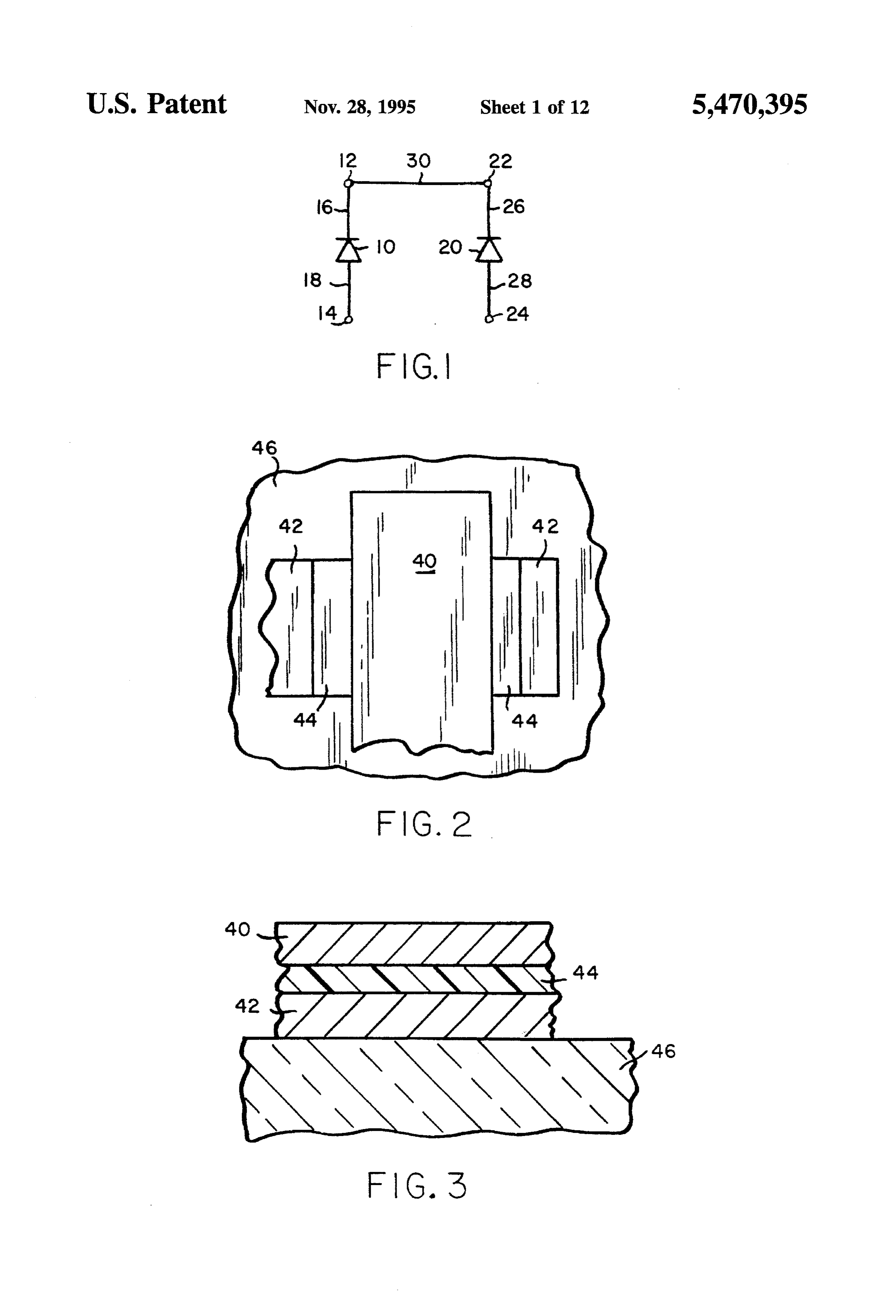
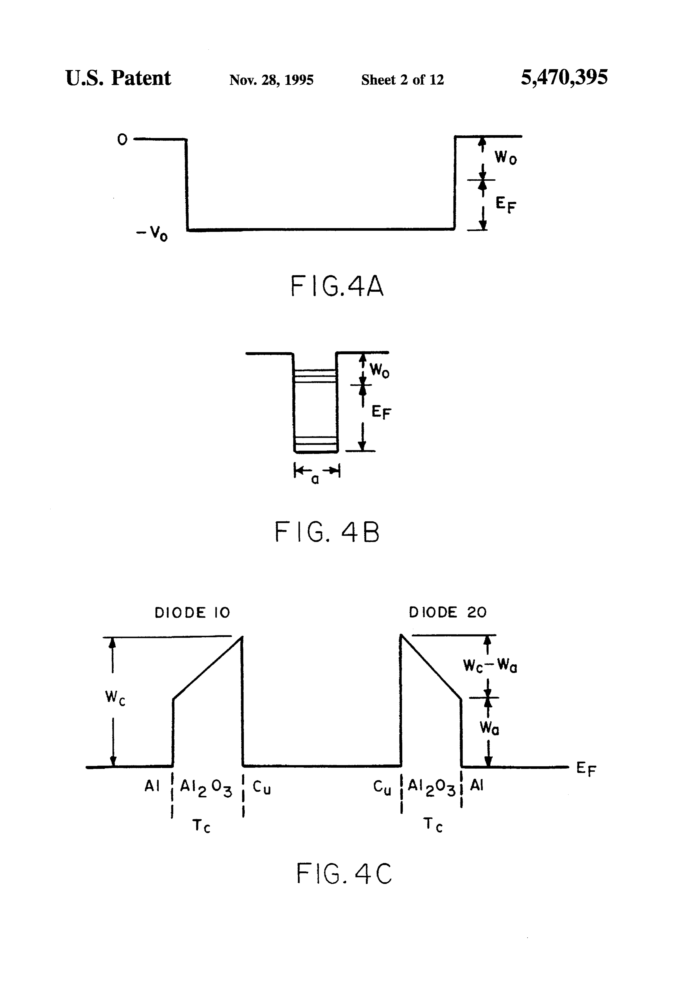
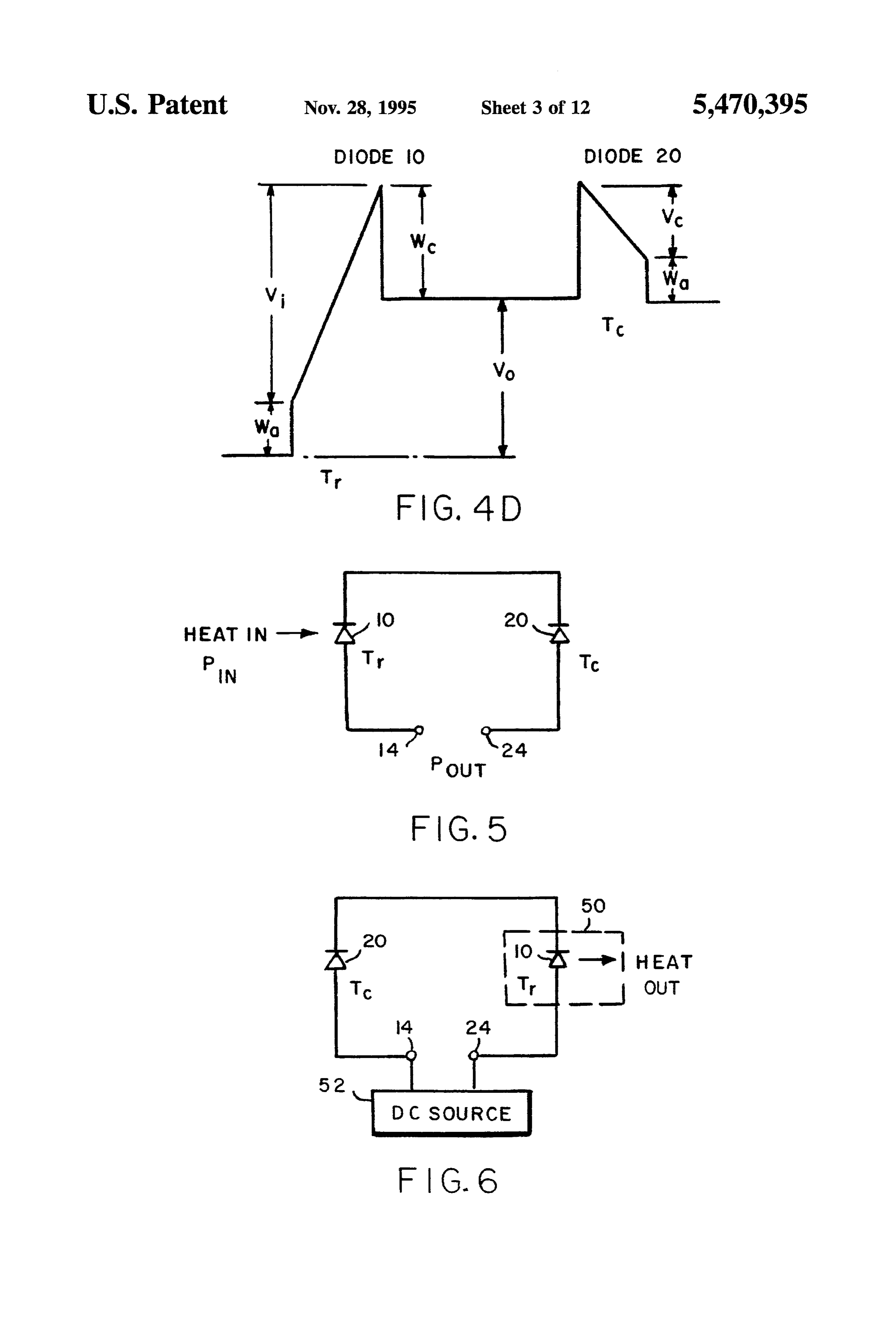
electric voltage fluctuations are coupled between the first FIG. 1 is a schematic diagram of a reversible thermoelec and second devices. The apparatus includes output terminals for providing cyclically varying electric energy having the 5 tric converter in accordance with the present invention; same waveform and a higher energy level than the cyclically FIG. 2 is a top view of a quantum well diode suitable for varying energy received by the first device. use in the reversible thermoelectric converter of FIG. 1; According to another aspect of the present invention, a FIG.3 is across section of the quantum well diode of FIG. reversible thermoelectric converter array comprises a sub 2, strate and one or more reversible thermoelectric converter FIG. 4A is an energy level diagram for a metal in vacuum, array elements formed on the substrate. Each array element 20 FIG. 4B is an energy level diagram for a thin metal film comprises a first quantum well diode, a second quantum well having quantized energy levels; diode, and means for electrically connecting the first diode to the second diode without a thermal barrier between them. FIG. 4C is an energy level diagram for two quantum well The array preferably includes spaced-apart lower electrodes diodes connected together for the case where the electrons in formed on the substrate, a dielectric film formed on the 25 both quantum well diodes are at the same temperature; lower electrodes, and spaced-apart upper electrodes formed FIG. 4D is an energy level diagram for two quantum well on the dielectric film and overlying at least part of the lower diodes connected togetherfor the case where the electrons in electrodes to form a series array of electrodes. The elec one quantum well diode have a higher temperature than the trodes are preferably thin metal films. electrons in the other quantum well diode; The reversible thermoelectric converter array elements 30 FIG. 5 is a schematic diagram showing the reversible can be connected in series on the substrate to provide a thermoelectric converter used for conversion of thermal desired output voltage. Multiple arrays can be connected in energy to electric energy;
parallel to provide a desired output current.
The first diode and the second diode of each array element 35 ibleFIG. 6 is a schematic diagram showing use of the revers thermoelectric converter as a heat pump;
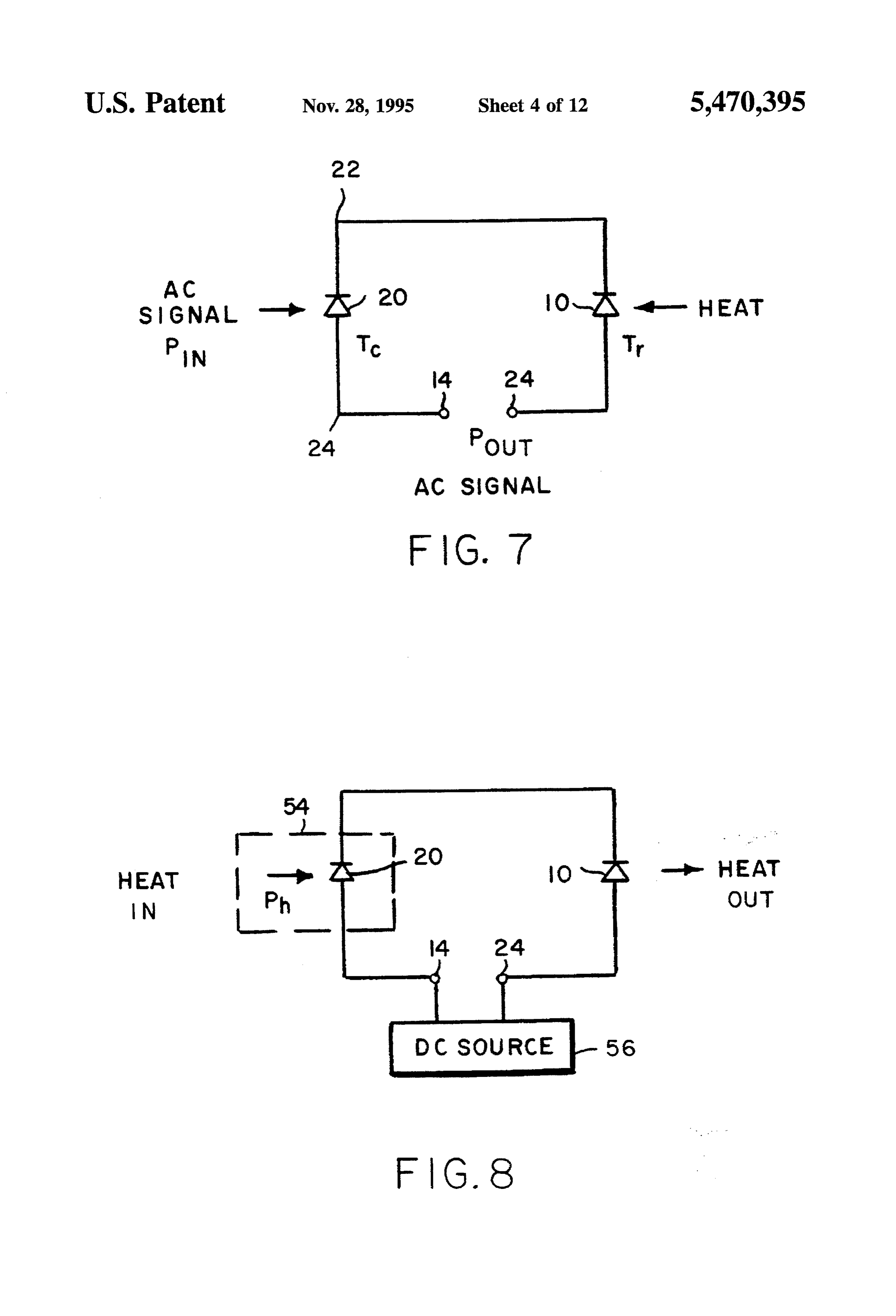
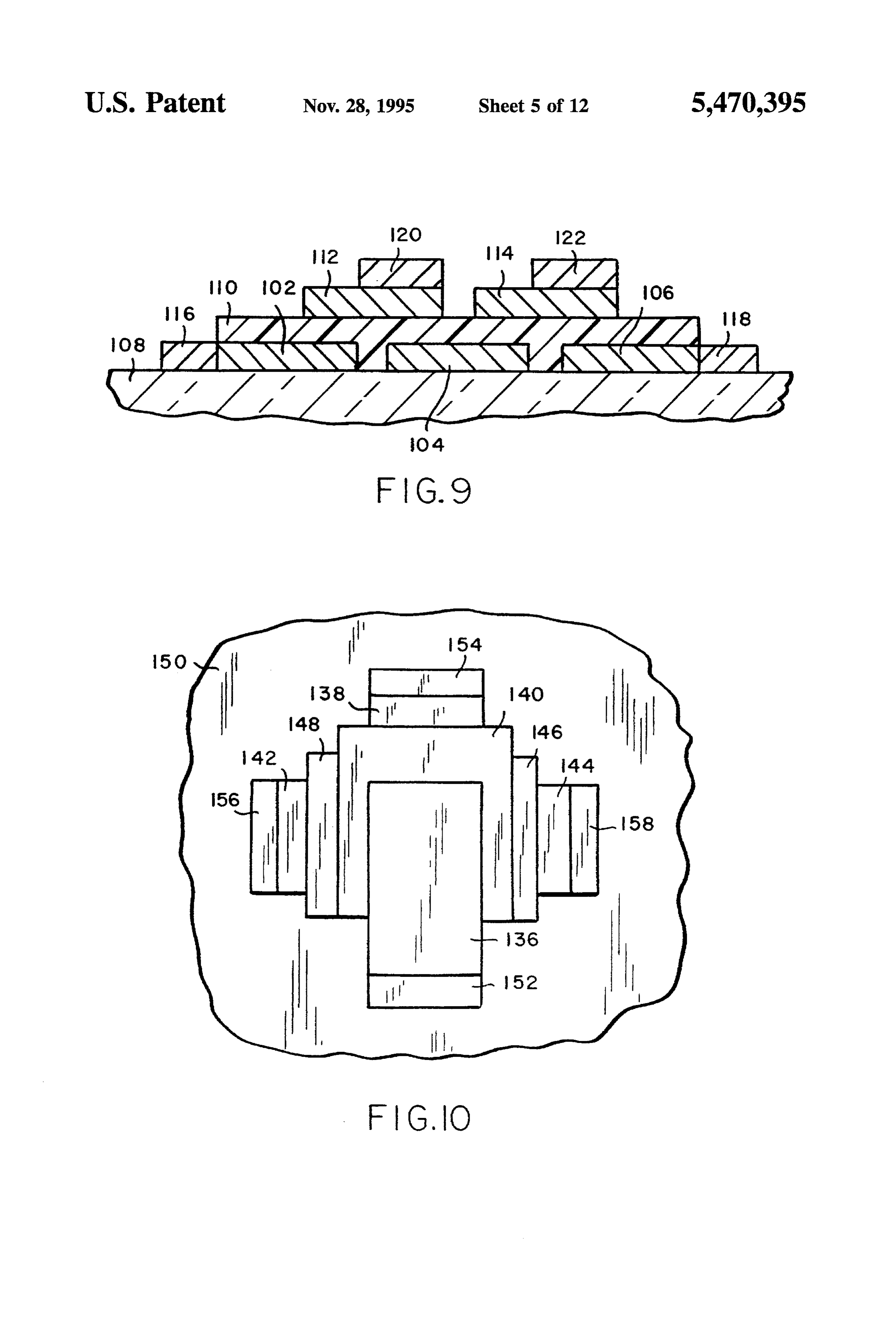
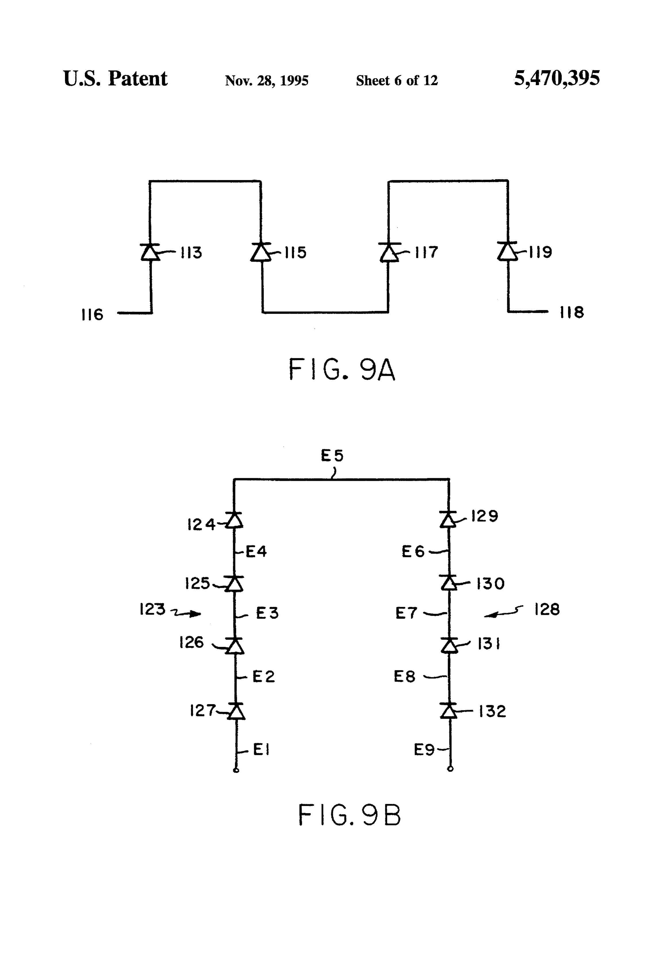
can each comprise a number of electrode pairs connected in FIG. 7 is a schematic diagram showing use of the revers series and means for applying successively larger voltage increments to the electrode pairs of the first and second ible thermoelectric converter as an amplifier; diodes. In one embodiment, the means for applying succes FIG. 8 is a schematic diagram showing use of the revers sively larger voltage increments comprises auxiliary elec ible thermoelectric converter as a refrigerator, trodes for applying electric fields to the electrode pairs of the 40 FIG. 9 is a cross section of a planar array of reversible first and second diodes and means for applying voltages to thermoelectric converter devices in accordance with the the auxiliary electrodes. In another embodiment, the first invention;
diode of an array element is formed on a first substrate portion and the second diode is formed on a second substrate theFIG. 9A is a schematic diagram of a first embodiment of planar array of FIG. 9;
portion such that the first and second diodes can be physi 45 cally separated during operation. FIG.9B is a schematic diagram of a second embodiment The array can include a thermal reservoir associated with of the planar array of FIG. 9;
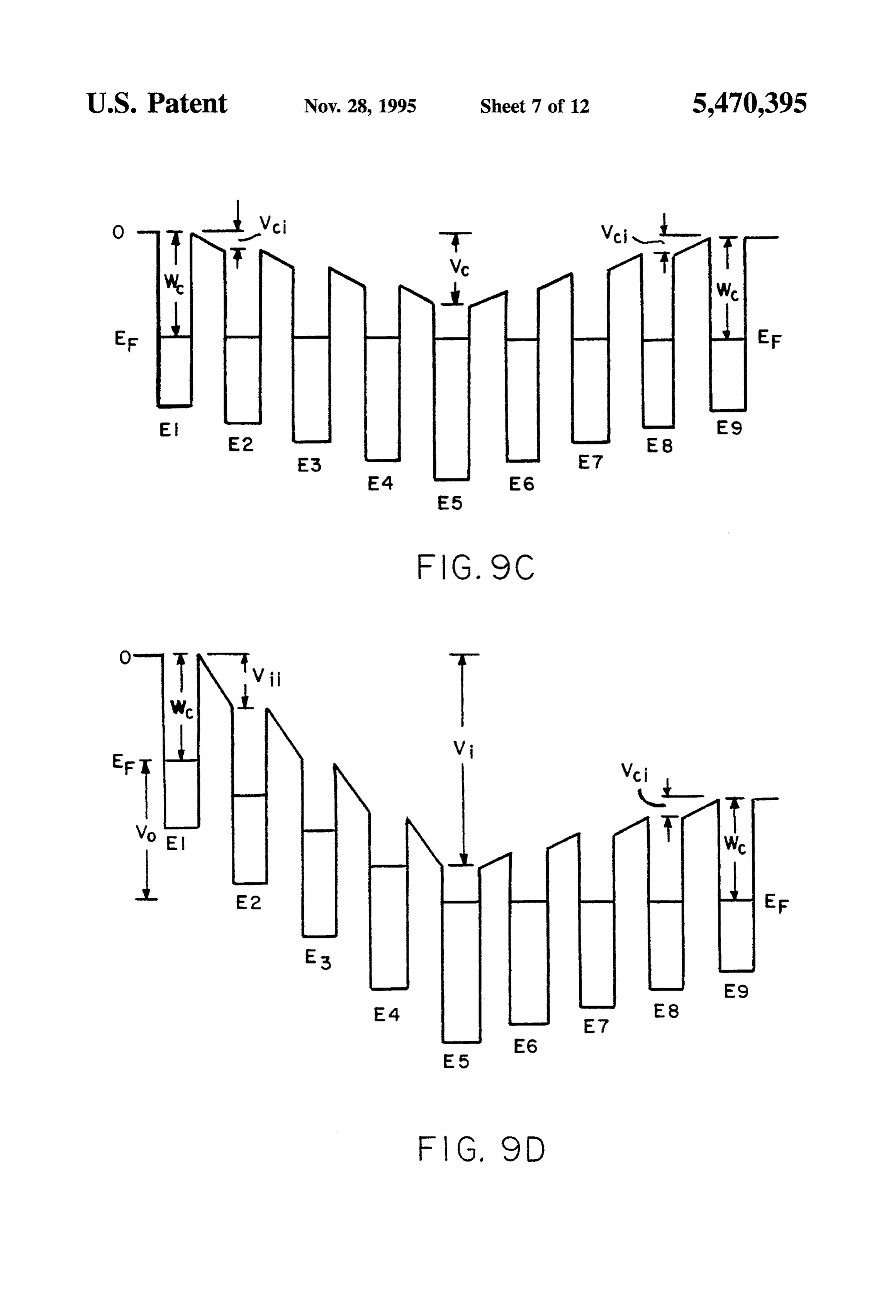
each of the array elements. The thermal reservoir is advan FIG. 9C and 9D are energy level diagrams of the revers tageous when the array is used in an enclosed environment. ible thermoelectric converter of FIG. 9B, with no thermal The thermal reservoir can comprise spaced-apart metal 50 energy input and with thermal energy input, respectively; electrodes disposed in close proximity to the electrodes of FIG. 10 is a top view of a nonplanar reversible thermo the first and second diodes and electrically isolated there electric converter fabricated in a vertical stacked array; from.
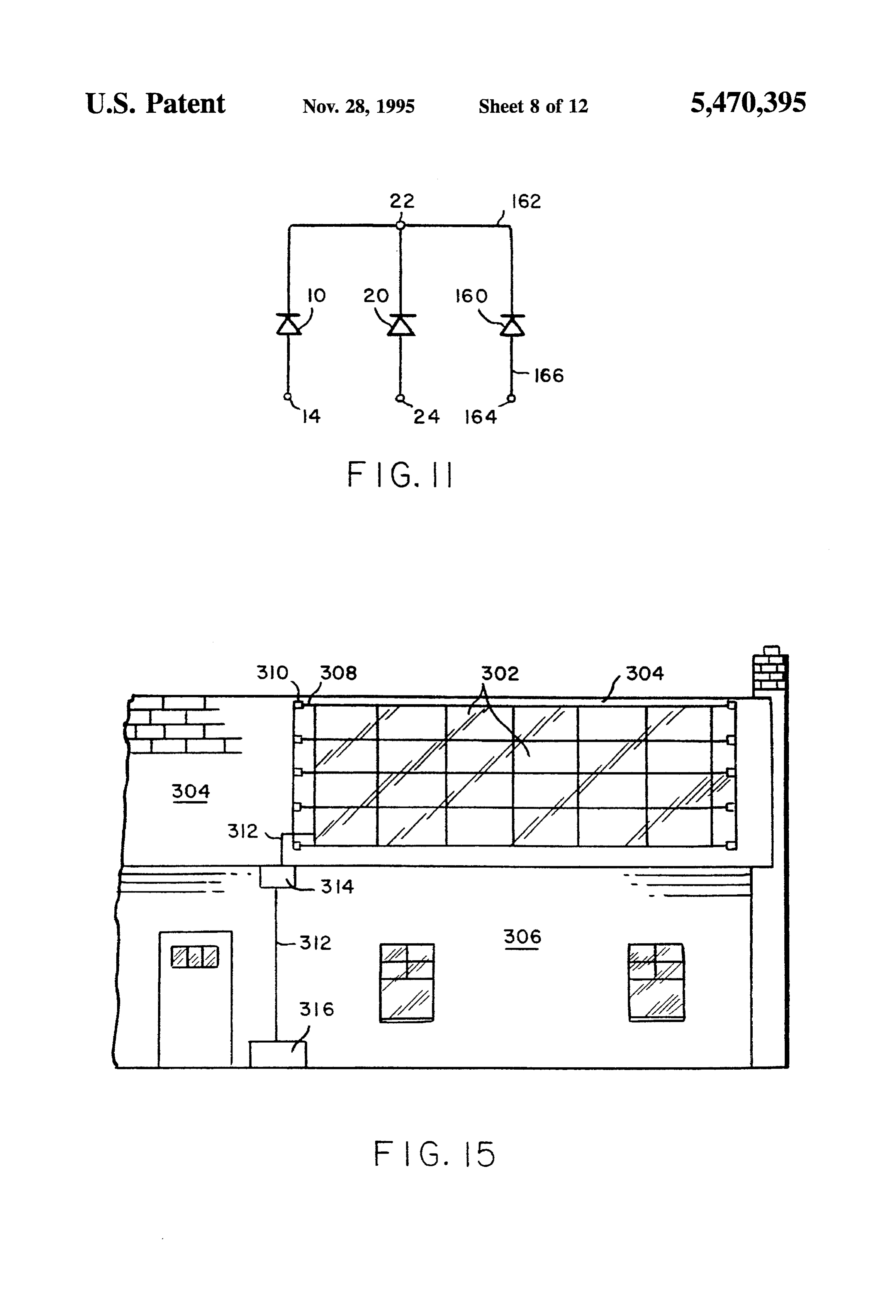
FIG. 11 is a schematic diagram of a two-stage reversible
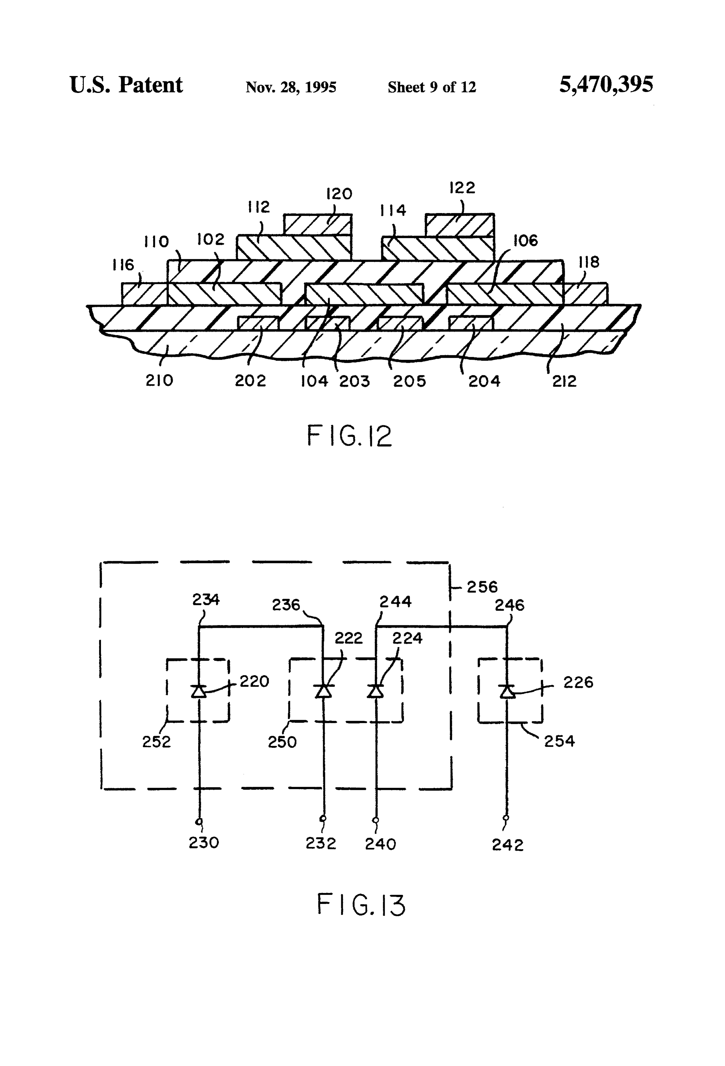
According to a further aspect of the invention, there is thermoelectric converter in accordance with the invention; provided a two-stage reversible thermoelectric converter 55 FIG. 12 is a cross sectional view of an array of reversible comprising a power conversion stage for receiving thermal thermoelectric converters including metal layers which act energy and converting the thermal energy to electric energy, as thermal reservoirs;
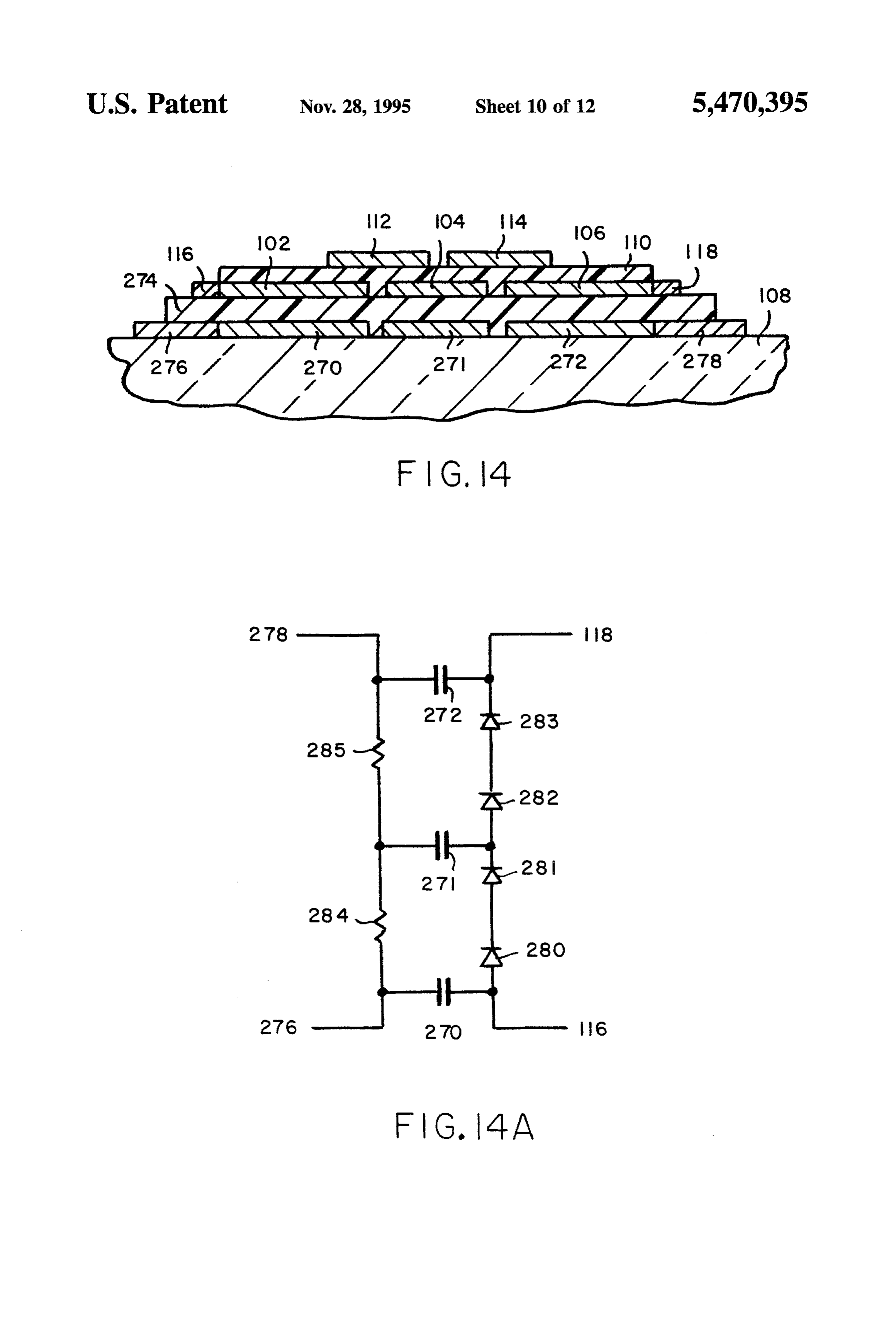
and a heat pump stage. The power conversion stage includes a first quantum well diode and a second quantum well diode FIG. 13 is a schematic diagram of a two-stage reversible connected as described above. The heat pump stage reduces 60 thermoelectric converter including separate circuits for the temperature of the second quantum well diode in the power conversion and heat pump functions; power conversion stage. The heat pump stage includes a FIG. 14 is a cross sectional view of a planar array of third quantum well diode and a fourth quantum well diode reversible thermoelectric converter devices, including connected as described above, and means for supplying a means for applying increments of voltage to the devices of DC voltage to the heat pump stage sufficient to reverse the 65 the array;
contact potential across the quantum well diodes. The heat FIG. 14A is a schematic diagram of the planar array of pump stage reduces the temperature of the electrons in the FIG. 14;
Page 17
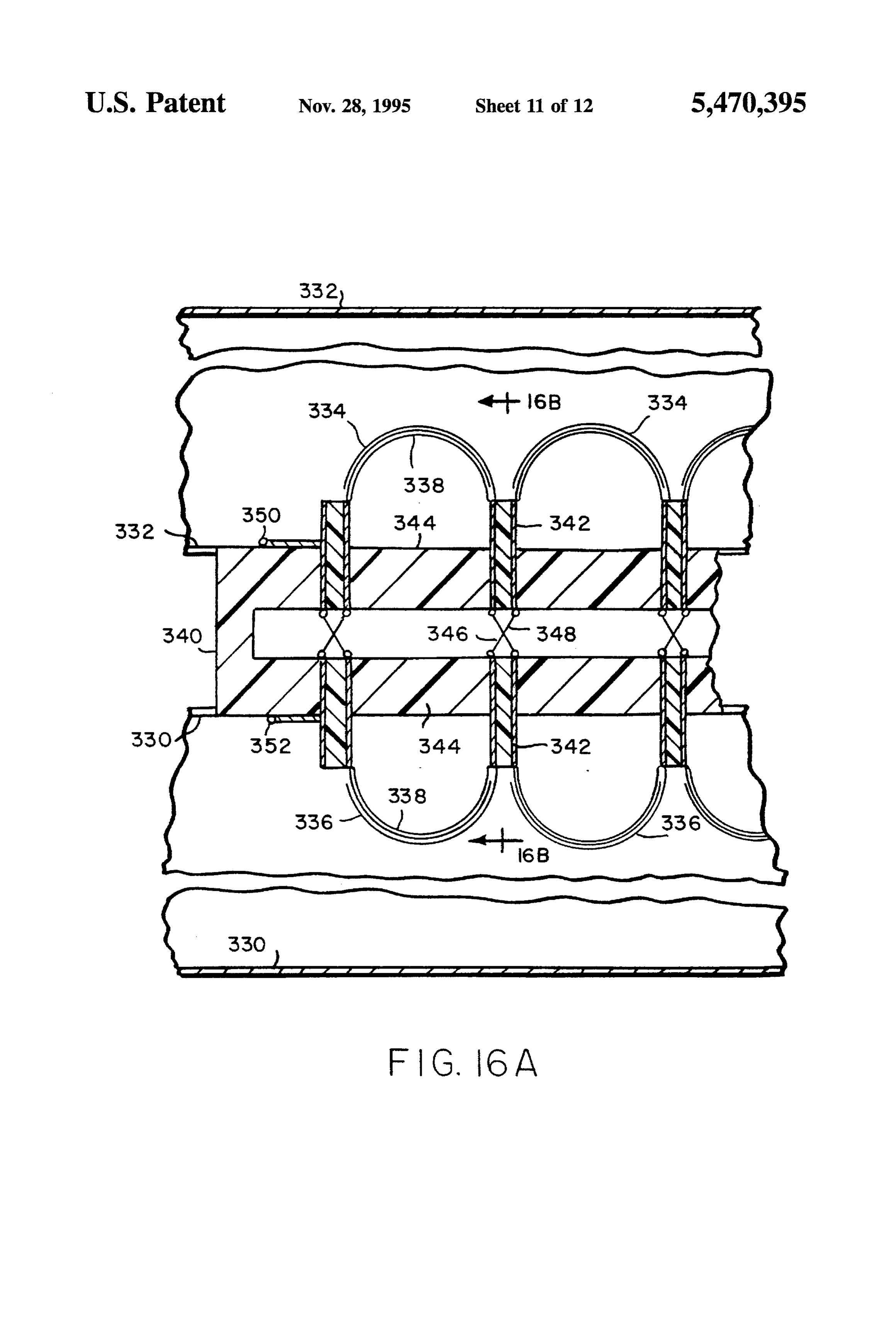
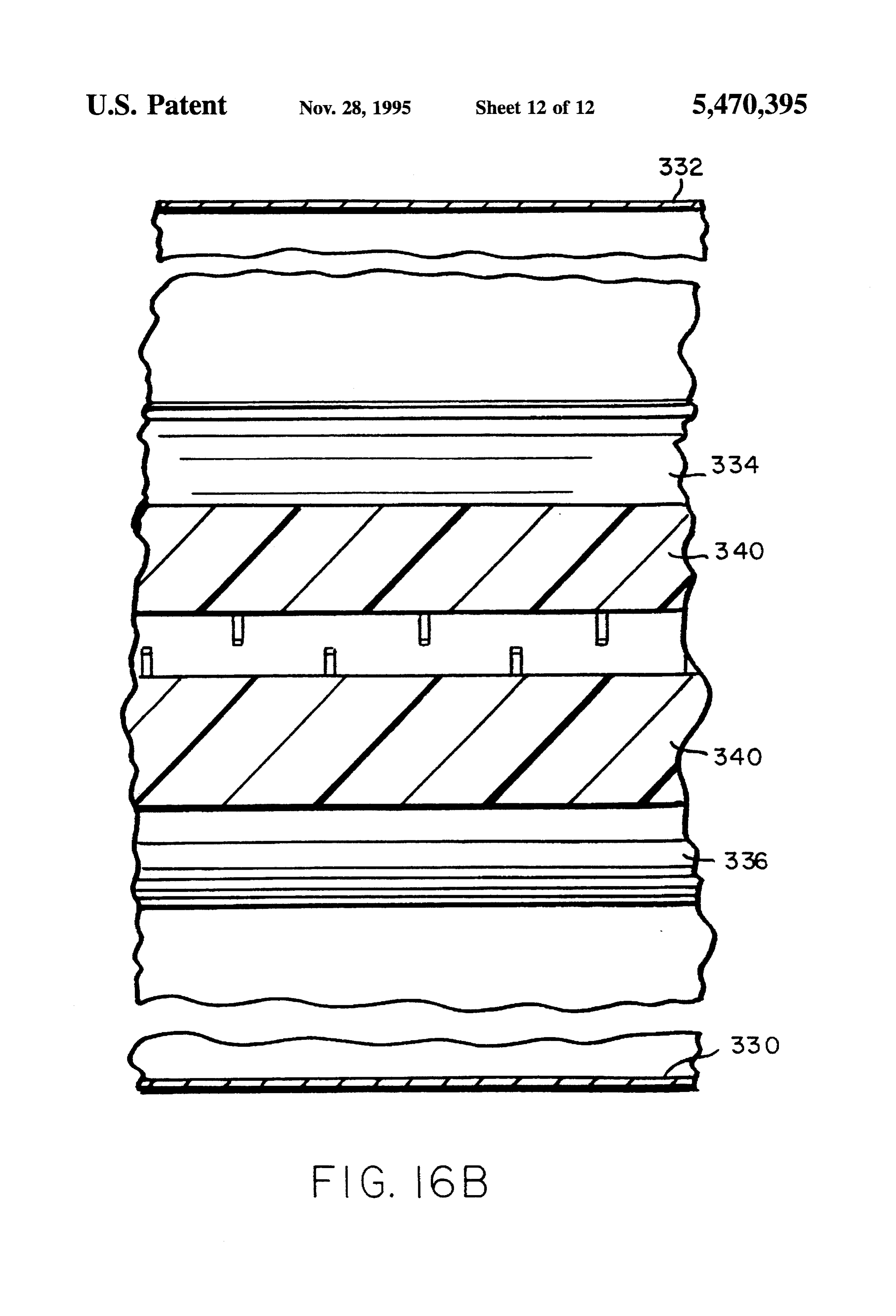
FIG. 15 is a pictorial diagram of an array of reversible of hot electrons, such as hot electrons which are photoge thermoelectric converter panels mounted on the roof of a nerated by incoming solar energy, are applied to the diode home; 10. When the converter is used in a power conversion FIG. 16A is a cross sectional view of a heat pump process, terminals 14 and 24 are the output terminals of the assembly of reversible thermoelectric converters mounted in circuit for supplying electric energy. heating and air conditioning ducts; and A quantum well diode is shown in FIGS. 2 and 3. FIG. 16B is a cross section of the heat pump assembly Conducting films 40 and 42 are separated by a dielectric taken along the line 16B-16B of FIG. 16A. layer 44 which serves as a diode barrier. The device is typically formed on a glass substrate 46. The layers 40, 42
O and 44 have thicknesses in a range of a few angstrons to
DETALED DESCRIPTION OF THE several hundred angstroms to insure that the electron energy NVENTION levels are quantized. In a preferred embodiment, layer 42 is The basic reversible thermoelectric converter of the an aluminum film, barrier layer 44 is aluminum oxide and present invention comprises two nonlinear circuit elements 15 layer 40 is a copper film.
with an electrical connection between the two circuit ele The use of state of the art evaporation techniques results ments. The two circuit elements are typically quantum well in a variation in the thickness of about 10%, or approxi diodes operating such that the electric carriers of the two mately 10 atomic layers, in the aluminum and copper films. diodes have different temperatures. The physical process of However, a thickness variation approaching only one atomic the reversible thermoelectric converter is that of a heat 20 layer is required for effective separation of energy levels in engine using a reversible thermodynamic process to convert the quantum wells of the diode. The existence of electronic thermal energy into electric energy or to convert electric standing wave energy levels in thin metal films resulting energy into thermal energy or to combine both processes from the quantized nature of the crystalline structure of the within one reversible thermoelectric converter circuit. The film has been described in the aforementioned article by R. reversible process of the circuit is operated as an ordered 25 C. Jaklevic et al. The standing waves reduce the spread that succession of equilibrium states. would otherwise occur in the quantized energy levels. These The classical reversible thermoelectric converter, as dis standing wave energy levels, called lattice commensurate closed in U.S. Pat. No. 4,004,210, is based on classical states, have a potential for applications in optoelectronics, thermodynamics and includes a discrete and separate ther since these thin metal films have extremely large absorption mal barrier between the hot and cold diodes. The theory of 30 and emission strengths at appropriate wavelengths. the reversible processes of the classical circuit shows that The quantum well diodes used in the reversible thermo the incoming energy fluctuations in the form of increments electric converter of the present invention include thin film of thermal energy are converted into electromagnetic energy metal quantum wells separated by a thin dielectric tunneling without, in the limit, any irreversible losses occurring, such barrier. The average potential of a conduction electron in a as heat losses across the thermal barrier. In the limit, the 35 bulk metal in vacuum at zero temperature is shown in FIG. intrinsic efficiency for the classical circuit approaches that of 4A. A potential well of depth V in the metal rises rapidly the Carnot cycle efficiency, E=1-T/T, where T is the near the metal boundaries to zero. As stated by R. Eisberg circuit temperature and T is the source temperature. For and R. Resnick in Quantum Physics of Atoms, Molecules, solar energy, the source temperature is the temperature of the Solids, Nuclei and Particles, John Wiley & Sons, Inc., New S. 40 York 1974, pp. 442-444, the energy levels at energy E in a The reversible thermoelectric converter of the present bulk metal increase in electron density proportional to E'. invention uses a quantum reversible thermodynamic cycle. and are filled up to the Fermi level E. The electron work The separate thermal barrier of the classical circuit is function W is the difference between the potential well replaced with a quantum well potential thermal barrier depth V and the Fermi level E. Thus, V=W+E, where within the thin film electrodes of a quantum well diode. 45 V=0 in the vacuum outside the metal.
Input hot electrons to the electrodes of the quantum well When a thin metal film has a thickness in the range of diode are the result of input energy fluctuations such as from about 100 angstroms, a quantum size effect of the film photogenerated electrons or input hot electrons over a con thickness results from quantized electron motion in a direc servative potential barrier. A conservative potential barrier is tion perpendicular to the plane of the metal film. The defined as a potential barrier where the transmission prob 50 quantum size effect gives rise to a series of discrete bound ability for a barrier crossing by a particle is a function of the states in the potential well as shown in FIG. 4B. The energy energy of the particle and where the barrier crossing is levels E of the bound states are given by E=3.76 (n/a)”x reversible and no dissipative energy loss occurs for the 10 electron volts, where n is the energy level and a is the particle barrier crossing. In comparison with the classical thickness of the well times 10 centimeters. For example, for circuit, the quantum reversible thermoelectric converter of 55 a well thickness of 60 angstroms, a=0.6. There are approxi the present invention provides improved performance, mately 15 energy levels in a well depth of approximately 10 reduced cost, simplified manufacturing and expanded appli electron volts, and the Fermi energy E is approximately cations. equal to 9 electron volts.
A reversible thermoelectric converter in accordance with One of the advantages of the metal quantum well for solar the present invention is shown schematically in FIG. 1. A 60 energy conversion is the high absorption of solar photons, diode 10 is connected to terminals 12 and 14 by conducting which are in the energy range of one electron volt. The high leads 16 and 18, respectively. A diode 20 is connected to absorption for transitions between energy levels near the top terminals 22 and 24 by conducting leads 26 and 28, respec level of the quantum well results from two factors. One tively. Terminals 12 and 22 are connected by a conducting factor is the oscillator strength, which is a measure of the lead 30 or by a capacitor (not shown). Diodes 10 and 20 are 65 absorption strength for transitions between energy levels in quantum well diodes as described below. For a typical power the quantum well. The other factor is the carrier density or conversion process, the incoming thermal energy in the form population of electrons in each energy level. The oscillator
Page 18
strength for transitions between energy levels 14 and 15 of higher energy levels and have a greater probability of the above example is approximately 12, which is more than crossing the potential barrier to the other electrode. an order of magnitude larger than that attainable from the most heavily doped semiconductor quantum wells. The theApplications of the reversible thermoelectric converter of present invention are shown schematically in FIGS. 5-8.
carrier density for these energy levels is on the order of 10' In FIG. 5, the reversible thermoelectric converter is used for electrons per square centimeter, which is several orders of conversion of thermal energy to electric energy. Thermal magnitude larger than that available from the most heavily doped semiconductors. Since the absorption strength for energy P is applied to quantum well diode 10. The thermal energy, which can be in the form of solar energy, is con specific transitions is proportional to the oscillator strength verted in diode 10 to hot photoelectrons at the temperature of a specific transition, such as the 1 volt transition from 10 T of the energy level 14 to energy level 15, times the population of temperaturesource. T.
The electrons in diode 20 are at a low relative to diode 10. The output electric the electrons for the transition, there is a huge advantage in energy P appears at terminals 14 and 24. the use of metal quantum wells for absorbing solar energy photons over semiconductor quantum wells. Operation of the reversible thermoelectric converter as a An energy level diagram for the potential energy levels of 15 heat pump is shown in FIG. 6. Thermal energy is absorbed two quantum well diodes connected together is shown in by quantum well diode 20 at low temperature T and thermal FIG. 4C. Each quantum well diode includes two quantum energy is given off by quantum well diode 10 at a higher wells in thin metal films with different work functions. In temperature T. The diode 10 is typically located in a region each quantum well diode, the metal films are separated by a 50 of essentially constant temperature T thin dielectric tunnel barrier. The energy level diagram of 20 The reversible thermoelectric converter used as a heat FIG. 4C corresponds to the reversible thermoelectric con pump differs from the use of the reversible thermoelectric verter shown in FIG. 1. Diode 10 and diode 20 each converter for power conversion in that means is used to comprises a copper film with a work function W and an reverse the current through the diodes 10 and 20. Current aluminum film with a work function W separated by an reversal can be obtained by applying a voltage from a DC aluminum oxide dielectric barrier. When the diodes are source 52 between the output terminals 14 and 24. Alterna connected, the Fermilevels become the same throughout the 25 tively, a voltage can be applied between the terminals of circuit, and the work function difference, W-W, is the diode 20 to obtain current reversal. The current reversal contact potential V between the copper and aluminum occurs when the voltage applied by DC source 52 has a quantum wells that exists across the aluminum oxide diode larger magnitude and opposite polarity as compared with the barrier. The electrons in diodes 10 and 20 are assumed to open circuit output voltage of the reversible thermoelectric have the same temperature in the energy level diagram of 30 converter. The ratio of the open circuit voltage to the contact FIG. 4C. potential across the diode electrodes is given by (T/T-1). The Fermi levels become equal when the most energetic The reversible thermoelectric converter shown in FIG. 1 electrons in the aluminum film, which has a lower work can be used to provide an AC power output. For AC function, flow into the copper film. The electron flow fills the 35 operation, the current through the reversible thermoelectric energy levels in the copper film just above its Fermi level converter is reversed cyclically so that the converter gener and depletes the energy levels in the aluminum film until ates a cyclic electric orthermal power output. A cyclic input equilibrium is reached. Equilibrium is reached when the can be applied between the terminals 22 and 24 of the cold highest filled energy levels in the copper and aluminum films diode 20 so as to generate a cyclic output with the same are at the same energy and the total energy of the circuit is 40 waveform as the input. The frequency of the cyclic output minimized. For the equilibrium state, the aluminum films power can be as great as the frequency corresponding to the become positively charged and the copper films become relaxation time of the reversible thermoelectric converter, negatively charged. A potential difference, or contact poten which can be less than 10' second. When a cyclic or AC tial, of V-1 millivolt between the copper and aluminum input is used, the reversible thermoelectric converter can films results. 45 function as an amplifier.
The energy level diagram for quantum well diodes 10 and Use of the reversible thermoelectric converter as an 20 when the electrons in diode 10 are heated is shown FIG. amplifier is shown schematically in FIG. 7. An AC signal P 4D. The number of electrons at a higher temperature and a is applied to quantum well diode 20 at a low temperature T higher energy level than the Fermi level is much larger at the and input thermal energy is applied to quantum well diode higher temperature. When the electrons in diode 10 are 50 10 at a high temperature T. The AC signal P can be in the heated, the current flows in the opposite direction through form of thermal energy, such as optical photons, or in the diode 10 as compared with the case of reaching equilibrium form of electric energy, such as a voltage applied across at the lower temperature for diode 10. In the energy level terminals 22 and 24 of diode 20. The output electric energy diagram of FIG. 4D, it is assumed that the temperature T of P is an AC signal with the waveform of the input signal electrons in diode 10 is 6000 K. and that the temperature T 55 P. The amplification factor is given by (TT)-1, where of electrons in diode 20 is 300 K. The new equilibrium for the input AC signal is applied to the cold diode attempera diode 10 results in the voltage across diode 10 becoming ture T in the form of thermal or electrical energy. V=(T/T)V=20 millivolts. The increased voltage across By way of example, an input signal of 6 microwatts with diode 10 raises the Fermi level of the copper film of diode a bandwidth of 1 gigahertz is applied to diode 20 either as 10 so that there is an output voltage V at the terminals 14 60 thermal energy or electric energy, and thermal energy is and 24 of the circuit of V=V-V or V=(1-T/T,)V. As a applied to diode 10. A signal-to-noise ration of 60 dB is result, the output voltage V is 19 millivolts for the equi obtained for the input signal for a temperature T of the cold librium state when T=6000 K. and T=300 K. diode 20 of 300 K. For a temperature T of hot electrons in Thus the electrons in each of the electrodes 40 and 42 are diode 10 of 6000 K., the amplification of the input signal is distributed in discrete energy levels determined by the 65 26 dB, which gives an output signal of 2.4 milliwatts. The temperature of the electrons and the material of the elec amplified output signal also has a 60 dB signal-to-noise trode. As the electrons are heated, they are distributed in ratio.
Page 19
Use of the reversible thermoelectric converter as a refrig the energy levels of the quantum wells in the electrodes of erator is shown in FIG. 8. In this case, thermal energy is the cool quantum well diode at circuit temperature T. transferred out of a low temperature region 54 at tempera Transitions over a wide range of energy level differences ture T containing quantum well diode 20, and thermal in the quantum wells are involved in the transformation of energy is given off by quantum well diode 10 at a higher approximately one electron volt of thermal energy into the temperature T. A DC source 56 connected between output electric energy output. The electric energy output consists of terminals 14 and 24 causes the normal direction of current many electrons of lesser energy and at a corresponding in the reversible thermoelectric converter to be reversed, as smaller output voltage as given by the output voltage of the described above in connection with the heat pump of FIG. equilibrium state of the quantum reversible thermoelectric 6. The refrigeration cycle shown in FIG. 8 is similar in 10 converter. The electromagnetic energy stored in the higher concept to the heat pump cycle shown in FIG. 6 and energy levels of the quantum wells in the quantum well described above.
diodes from incoming thermal energy, develops as the
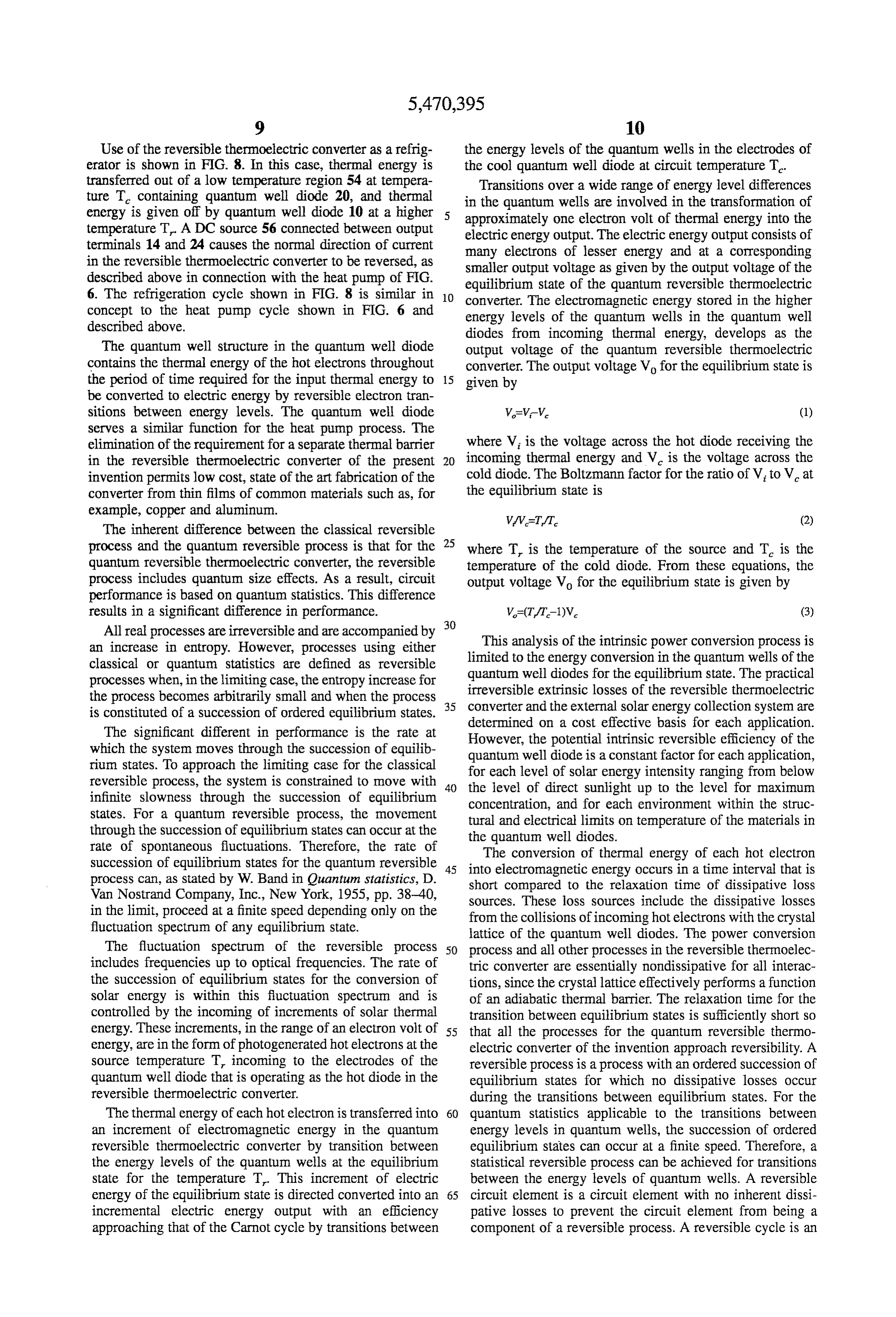
The quantum well structure in the quantum well diode output voltage of the quantum reversible thermoelectric contains the thermal energy of the hot electrons throughout converter. The output voltage V for the equilibrium state is the period of time required for the input thermal energy to 15 given by be converted to electric energy by reversible electron tran sitions between energy levels. The quantum well diode W=V-V. (1) serves a similar function for the heat pump process. The elimination of the requirement for a separate thermal barrier where V is the voltage across the hot diode receiving the in the reversible thermoelectric converter of the present 20 incoming thermal energy and V is the voltage across the invention permits low cost, state of the art fabrication of the cold diode. The Boltzmann factor for the ratio of V, to V at converter from thin films of common materials such as, for the equilibrium state is example, copper and aluminum.
The inherent difference between the classical reversible process and the quantum reversible process is that for the 25 where T is the temperature of the source and T is the quantum reversible thermoelectric converter, the reversible temperature of the cold diode. From these equations, the process includes quantum size effects. As a result, circuit output voltage Vo for the equilibrium state is given by performance is based on quantum statistics. This difference results in a significant difference in performance.
All real processes are irreversible and are accompanied by 30 an increase in entropy. However, processes using either This analysis of the intrinsic power conversion process is classical or quantum statistics are defined as reversible limited to the energy conversion in the quantum wells of the processes when, in the limiting case, the entropy increase for quantum well diodes for the equilibrium state. The practical the process becomes arbitrarily small and when the process 35 irreversible extrinsic losses of the reversible thermoelectric is constituted of a succession of ordered equilibrium states. converter and the external solar energy collection system are The significant different in performance is the rate at determined on a cost effective basis for each application. which the system moves through the succession of equilib However, the potential intrinsic reversible efficiency of the rium states. To approach the limiting case for the classical quantum well diode is a constant factor for each application, for each level of solar energy intensity ranging from below reversible process, the system is constrained to move with 40 the level of direct sunlight up to the level for maximum infinite slowness through the succession of equilibrium concentration, and for each environment within the struc states. For a quantum reversible process, the movement tural and electrical limits on temperature of the materials in through the succession of equilibrium states can occur at the the quantum well diodes.
rate of spontaneous fluctuations. Therefore, the rate of succession of equilibrium states for the quantum reversible 45 intoThe conversion of thermal energy of each hot electron electromagnetic energy occurs in a time interval that is process can, as stated by W. Band in Ouantum statistics, D. short compared to the relaxation time of dissipative loss Van Nostrand Company, Inc., New York, 1955, pp. 38-40, sources. These loss sources include the dissipative losses in the limit, proceed at a finite speed depending only on the from the collisions of incoming hot electrons with the crystal fluctuation spectrum of any equilibrium state. lattice of the quantum well diodes. The power conversion The fluctuation spectrum of the reversible process 50 process and all other processes in the reversible thermoelec includes frequencies up to optical frequencies. The rate of tric converter are essentially nondissipative for all interac the succession of equilibrium states for the conversion of tions, since the crystal lattice effectively performs a function Solar energy is within this fluctuation spectrum and is of an adiabatic thermal barrier. The relaxation time for the controlled by the incoming of increments of solar thermal transition between equilibrium states is sufficiently short so energy. These increments, in the range of an electron volt of 55 that all the processes for the quantum reversible thermo energy, are in the form of photogenerated hot electrons at the electric converter of the invention approach reversibility. A source temperature T, incoming to the electrodes of the reversible process is a process with an ordered succession of quantum well diode that is operating as the hot diode in the equilibrium states for which no dissipative losses occur reversible thermoelectric converter. during the transitions between equilibrium states. For the The thermal energy of each hot electron is transferred into 60 quantum statistics applicable to the transitions between an increment of electromagnetic energy in the quantum energy levels in quantum wells, the succession of ordered reversible thermoelectric converter by transition between equilibrium states can occur at a finite speed. Therefore, a the energy levels of the quantum wells at the equilibrium statistical reversible process can be achieved for transitions state for the temperature T. This increment of electric between the energy levels of quantum wells. A reversible energy of the equilibrium state is directed converted into an 65 circuit element is a circuit element with no inherent dissi incremental electric energy output with an efficiency pative losses to prevent the circuit element from being a approaching that of the Carnot cycle by transitions between component of a reversible process. A reversible cycle is an
Page 20
idealized abstraction in classical thermodynamics, since the output voltage with minimum transmission and thermaliza system is required to move with infinite slowness through a tion losses. The contact potential can be varied by selection succession of equilibrium states in order for the process to of metals with different work functions. be reversible. This is not the case for the reversible cycle of For the power conversion of thermal energy having lower the present invention, since this reversible cycle is based on intensity than concentrated solar energy, the thickness of the quantum statistics controlling the energy transitions. As metal film electrodes can be reduced. Reducing the thick discussed in more detail below, the reversible process ness of the electrodes to below 100 angstroms increases the requires that the conversion of thermal energy into electric oscillator strength, reduces the carrier density and decreases energy occurs in a time that is short compared to the thermal the thermalization loss rate for the quantum energy states. As relaxation time of the dissipative loss sources. 10 the thickness of the diode electrode is reduced, the quantum It has been demonstrated that tunnel diodes can rectify an well size decreases and the lifetime of the quantum states is optical frequencies, and recent work has shown that the lengthened. This increases the thermalization time for lattice electron photon thermalization times of hot electrons in states so as to further reduce thermalization losses. devices can be longer by two or three orders of magnitude The thermalization time for the quantum states of the than the hot electron barrier crossing time in a tunnel diode. 15 quantum well diode is also a function of temperature. As The analysis of the barrier crossing time shows the potential described below, the heat pump process can be combined for this time to be as short as 10' second for tunnel diodes. with the power conversion process in a two-stage reversible For the measurements being recorded, this barrier crossing thermoelectric converter to reduce the temperature of the time is estimated to be of the order of 10 second for a 10 cold diode in the power conversion stage so as to increase angstrom thick barrier crossing by a ballistic electron with a 20 the thermalization time and thereby reduce thermalization 10 cm per second velocity. The response time of the diode losses. The decrease in temperature of the cold quantum well quantum reversible thermoelectric converter can be com increases the lifetime of the crystal lattice states and puted using the relaxation times of the quantum well diodes. decreases the time constant of the quantum well diode, To the first orderin the expansion of the fluctuation spectrum be which enables the conversion time of the thermal energy to decreased.
of the reversible thermoelectric converter with electrically 25 In order to reduce thermalization loss during energy equivalent hot and cold diodes, the relaxation time t is given conversion in the reversible thermoelectric converter, the by energy conversion time t can be controlled relative to the t=(kT/e) (C/A) thermalization time t of all loss sources. Specially, the
conversion time t must be less than the thermalization time where T is the temperature of the cold diode, C is the 30 te. The conversion time t is the time that energy is stored capacitance of the quantum well diode and A is the satura in the quantum wells of the quantum well diode. The tion current for the electrodes of the hot diode. The relax conversion time for the reversible conversion of incoming ation time t, is a function of the temperatures T, and T for than theenergy thermal into output electrical energy must be less the conversion of solar energy by the quantum reversible quantum well diodes.lifetime expected
The of the quantum states in the energy conversion time t for an thermoelectric converter T. can be as low as 10 second. 35 output voltage V, to deliver an output power P is given by: This relaxation time is short compared to the relaxation time of all dissipative loss sources including the dissipative losses t=(CV)/(2P) (5) from the collisions from incoming hot electrons within the crystal lattice of the quantum well diodes. where C is the capacitance across the quantum well diodes. The design of the quantum well diodes for the reversible 40 As indicated in Equation (3) above, the output voltage V is thermoelectric converter is a function of the application, and proportional to the voltage V across the cold diode, which the effective temperature and intensity of the source of hot is the contact potential of the quantum well diode. Equations electrons. Several applications of the reversible thermoelec (3) and (5) show that the conversion time t is a function of tric converter are discussed below. In an example of a thin the diode contact potential V. Thus, the conversion time t film metallic quantum well diode suitable for the conversion 45 can be reduced by lowering the contact potential V. Also, of solar energy concentrated up to 10' watts per square for the lower input power levels, the conversion time t can meter, layer 42 (FIGS. 2 and 3) is an evaporated aluminum be maintained less than the thermalization time t, and the film having a thickness of 140 angstroms, barrier layer 44 is reversible power conversion process can be maintained by evaporated aluminum oxide having a thickness of 12 ang lowering the contact potential V as the power level P. stroms and layer 40 is an evaporated copper film having a 50 decreases. In general, the voltage V across the cold diode thickness of 100 angstroms. For this energy conversion can be varied in order to maintain the conversion time teless application, metal electrodes are specified since amounts of than the thermalization time t, by varying the design of the power as large as concentrated solar energy can be delivered quantum well diode, or by applying a suitable voltage to the by the quantum reversible thermoelectric converter. The quantum well diode.
high power output capability results from the large electron 55 The discussion thus far has been directed primarily to carrier density of metals, which can be orders of magnitude input thermal energy in the form of solar energy at a source larger than the most heavily doped semiconductors. temperature of 6000 K. It will be understood that the For the electrodes of the quantum well diodes, high reversible thermoelectric converter of the present invention conductivity metals such as copper, aluminum silver, gold, can be utilized at a variety of different intensity levels and nickel and magnesium provide high carrier densities, large 60 photon energy levels with appropriate scaling. When the oscillator strengths for the energy level transitions and low input thermal energy has a lower temperature, the quantum resistance to the output current. For the dielectric material of well dimensions are scaled in width and/or depth so that the the diode barrier in the quantum well diodes, dielectric transitions between energy levels near the top of the quan materials such as Al-O, SiO, and SiO can be used. As tum wells are at energy levels corresponding to the energy discussed above, a contact potential V-1 millivolt for 65 of the photons of the incoming radiation energy. copper and aluminum electrodes using concentrated solar Scaling the depth of the quantum wells can be accom radiation input intensity is sufficient to obtain a practical plished by selecting a material for the diode electrodes with
Page 21
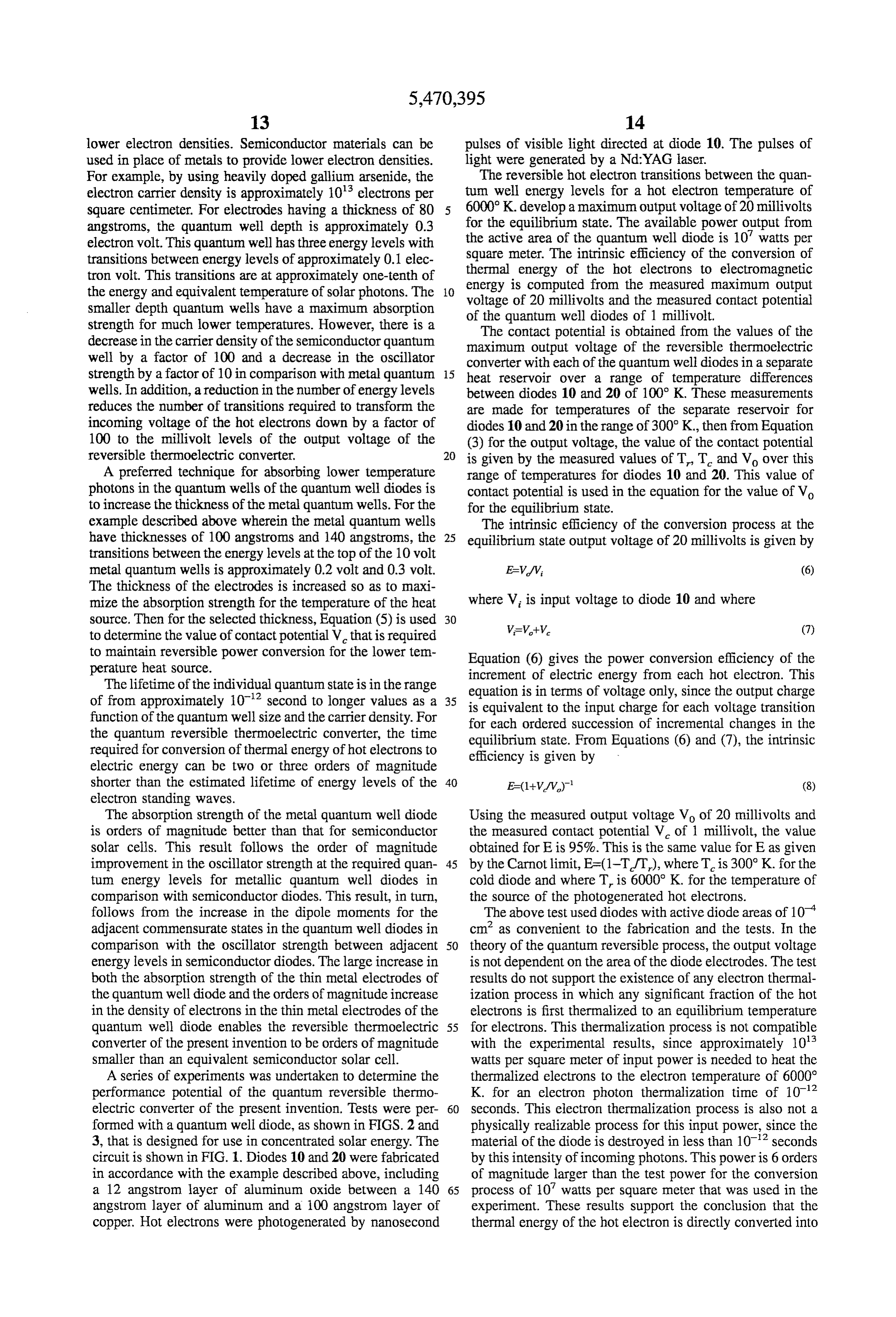
lower electron densities. Semiconductor materials can be pulses of visible light directed at diode 10. The pulses of used in place of metals to provide lower electron densities. light were generated by a Nd:YAG laser. For example, by using heavily doped gallium arsenide, the The reversible hot electron transitions between the quan electron carrier density is approximately 10' electrons per tum well energy levels for a hot electron temperature of square centimeter. For electrodes having a thickness of 80 6000°K. develop a maximum output voltage of 20 millivolts angstroms, the quantum well depth is approximately 0.3 for the equilibrium state. The available power output from electron volt. This quantum well has three energy levels with the active area of the quantum well diode is 10' watts per transitions between energy levels of approximately 0.1 elec square meter. The intrinsic efficiency of the conversion of tron volt. This transitions are at approximately one-tenth of thermal energy of the hot electrons to electromagnetic the energy and equivalent temperature of solar photons. The 10 energy is computed from the measured maximum output voltage of 20 millivolts and the measured contact potential smaller depth quantum wells have a maximum absorption of the quantum well diodes of 1 millivolt. strength for much lower temperatures. However, there is a The contact potential is obtained from the values of the decrease in the carrier density of the semiconductor quantum maximum output voltage of the reversible thermoelectric well by a factor of 100 and a decrease in the oscillator converter with each of the quantum well diodes in a separate strength by a factor of 10 in comparison with metal quantum 15 heat reservoir over a range of temperature differences wells. In addition, a reduction in the number of energy levels between diodes 10 and 20 of 100 K. These measurements reduces the number of transitions required to transform the are made for temperatures of the separate reservoir for incoming voltage of the hot electrons down by a factor of diodes 10 and 20 in the range of 300°K., then from Equation 100 to the millivolt levels of the output voltage of the (3) for the output voltage, the value of the contact potential reversible thermoelectric converter. 20 is given by the measured values of T, T and Vo over this A preferred technique for absorbing lower temperature range of temperatures for diodes 10 and 20. This value of photons in the quantum wells of the quantum well diodes is contact potential is used in the equation for the value of Vo to increase the thickness of the metal quantum wells. For the for the equilibrium state.
example described above wherein the metal quantum wells The intrinsic efficiency of the conversion process at the have thicknesses of 100 angstroms and 140 angstroms, the 25 equilibrium state output voltage of 20 millivolts is given by transitions between the energy levels at the top of the 10 volt metal quantum wells is approximately 0.2 volt and 0.3 volt.
The thickness of the electrodes is increased so as to maxi mize the absorption strength for the temperature of the heat where V is input voltage to diode 10 and where source. Then for the selected thickness, Equation (5) is used 30 V=V+V. (7) to determine the value of contact potential V that is required to maintain reversible power conversion for the lower tem Equation (6) gives the power conversion efficiency of the perature heat source. increment of electric energy from each hot electron. This The lifetime of the individual quantum state is in the range of from approximately 10' second to longer values as a 35 isequation is in terms of voltage only, since the output charge equivalent to the input charge for each voltage transition function of the quantum well size and the carrier density. For for each ordered succession of incremental changes in the the quantum reversible thermoelectric converter, the time equilibrium state. From Equations (6) and (7), the intrinsic required for conversion of thermal energy of hot electrons to efficiency is given by electric energy can be two or three orders of magnitude shorter than the estimated lifetime of energy levels of the 40 electron standing waves.
The absorption strength of the metal quantum well diode Using the measured output voltage V of 20 millivolts and is orders of magnitude better than that for semiconductor the measured contact potential V of 1 millivolt, the value solar cells. This result follows the order of magnitude obtained for E is 95%. This is the same value for E as given improvement in the oscillator strength at the required quan 45 by the Carnot limit, E=(1-T/T,), where T is 300°K. for the tum energy levels for metallic quantum well diodes in cold diode and where T is 6000 K. for the temperature of comparison with semiconductor diodes. This result, in turn, the source of the photogenerated hot electrons. follows from the increase in the dipole moments for the The above test used diodes with active diode areas of 10 adjacent commensurate states in the quantum well diodes in cm as convenient to the fabrication and the tests. In the comparison with the oscillator strength between adjacent 50 theory of the quantum reversible process, the output voltage energy levels in semiconductor diodes. The large increase in is not dependent on the area of the diode electrodes. The test both the absorption strength of the thin metal electrodes of results do not support the existence of any electron thermal the quantum well diode and the orders of magnitude increase ization process in which any significant fraction of the hot in the density of electrons in the thin metal electrodes of the electrons is first thermalized to an equilibrium temperature quantum well diode enables the reversible thermoelectric 55 for electrons. This thermalization process is not compatible converter of the present invention to be orders of magnitude with the experimental results, since approximately 10' smaller than an equivalent semiconductor solar cell. watts per square meter of input power is needed to heat the A series of experiments was undertaken to determine the thermalized electrons to the electron temperature of 6000 performance potential of the quantum reversible thermo K. for an electron photon thermalization time of 10° electric converter of the present invention. Tests were per 60 seconds. This electron thermalization process is also not a formed with a quantum well diode, as shown in FIGS. 2 and physically realizable process for this input power, since the 3, that is designed for use in concentrated solar energy. The material of the diode is destroyed in less than 10' seconds circuit is shown in FIG. I. Diodes 10 and 20 were fabricated by this intensity of incoming photons. This power is 6 orders in accordance with the example described above, including of magnitude larger than the test power for the conversion a 12 angstrom layer of aluminum oxide between a 140 65 process of 10 watts per square meter that was used in the angstrom layer of aluminum and a 100 angstrom layer of experiment. These results support the conclusion that the copper. Hot electrons were photogenerated by nanosecond thermal energy of the hot electron is directly converted into
Page 22
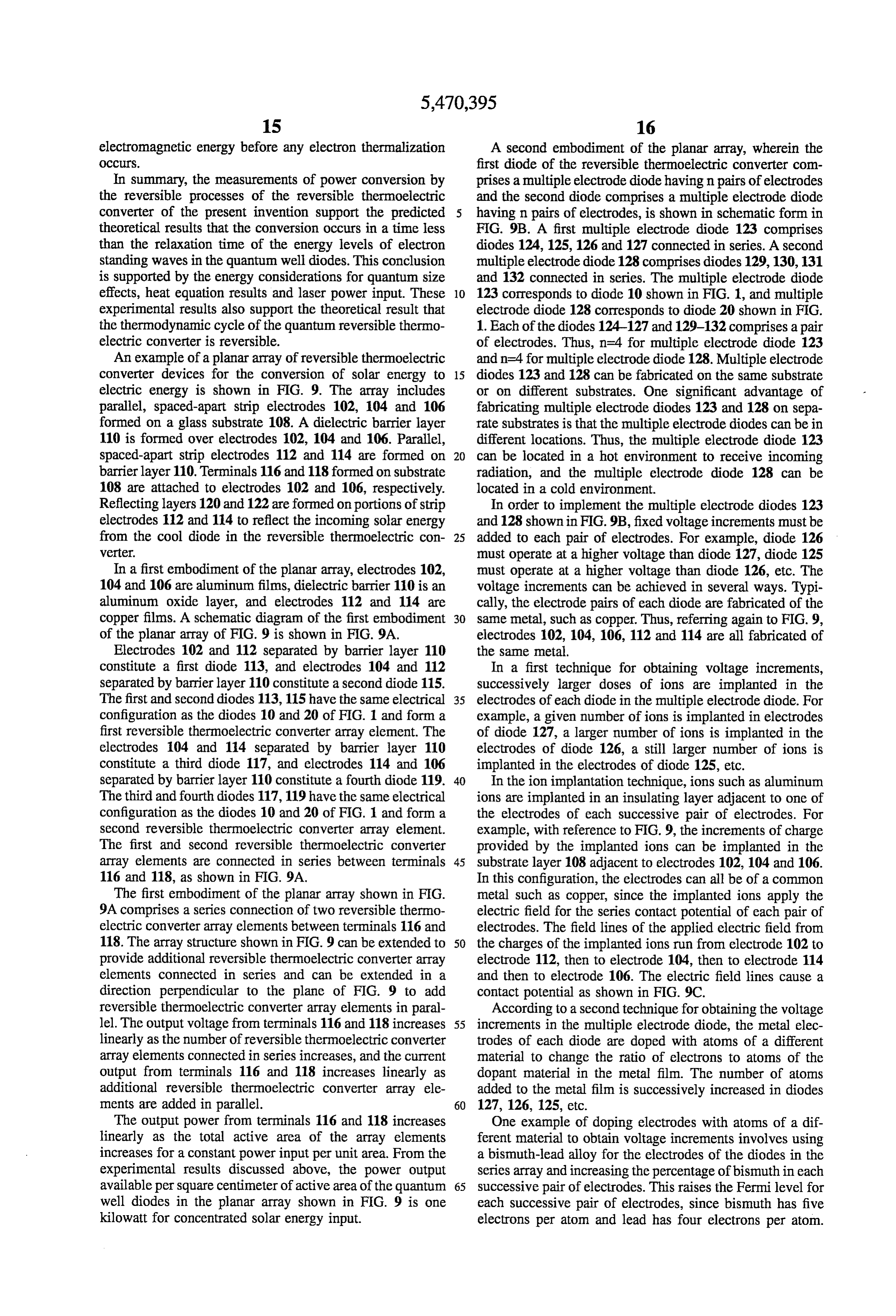
electromagnetic energy before any electron thermalization A second embodiment of the planar array, wherein the OCCS. first diode of the reversible thermoelectric converter com In summary, the measurements of power conversion by prises a multiple electrode diode having n pairs of electrodes the reversible processes of the reversible thermoelectric and the second diode comprises a multiple electrode diode converter of the present invention support the predicted having n pairs of electrodes, is shown in schematic form in theoretical results that the conversion occurs in a time less FIG. 9B. A first multiple electrode diode 123 comprises than the relaxation time of the energy levels of electron diodes 124, 125, 126 and 127 connected in series. A second standing waves in the quantum well diodes. This conclusion multiple electrode diode 128 comprises diodes 129, 130,131 is supported by the energy considerations for quantum size and 132 connected in series. The multiple electrode diode effects, heat equation results and laser power input. These 10 123 corresponds to diode 10 shown in FIG. 1, and multiple experimental results also support the theoretical result that electrode diode 128 corresponds to diode 20 shown in FIG. the thermodynamic cycle of the quantum reversible thermo 1. Each of the diodes 124-127 and 129-132 comprises a pair electric converter is reversible. of electrodes. Thus, n=4 for multiple electrode diode 123 An example of a planar array of reversible thermoelectric and n=4 for multiple electrode diode 128. Multiple electrode converter devices for the conversion of solar energy to 15 diodes 123 and 128 can be fabricated on the same substrate electric energy is shown in FIG. 9. The array includes or on different substrates. One significant advantage of parallel, spaced-apart strip electrodes 102, 104 and 106 fabricating multiple electrode diodes 123 and 128 on sepa formed on a glass substrate 108. A dielectric barrier layer rate substrates is that the multiple electrode diodes can be in 110 is formed over electrodes 102, 104 and 106. Parallel, different locations. Thus, the multiple electrode diode 123 spaced-apart strip electrodes 112 and 114 are formed on 20 can be located in a hot environment to receive incoming barrier layer 110. Terminals 116 and 118 formed on substrate radiation, and the multiple electrode diode 128 can be 108 are attached to electrodes 102 and 106, respectively. located in a cold environment.
Reflecting layers 120 and 122 are formed on portions of strip In order to implement the multiple electrode diodes 123 electrodes 112 and 114 to reflect the incoming solar energy and 128 shown in FIG.9B, fixed voltage increments must be from the cool diode in the reversible thermoelectric con 25 added to each pair of electrodes. For example, diode 126 Wetter. must operate at a higher voltage than diode 127, diode 125 In a first embodiment of the planar array, electrodes 102, must operate at a higher voltage than diode 126, etc. The 104 and 106 are aluminum films, dielectric barrier 10 is an voltage increments can be achieved in several ways. Typi aluminum oxide layer, and electrodes 112 and 114 are cally, the electrode pairs of each diode are fabricated of the copper films. A schematic diagram of the first embodiment 30 same metal, such as copper. Thus, referring again to FIG. 9, of the planar array of FIG. 9 is shown in FIG. 9A. electrodes 102, 104, 106, 112 and 114 are all fabricated of Electrodes 102 and 112 separated by barrier layer 110 the same metal.
constitute a first diode 113, and electrodes 104 and 112 In a first technique for obtaining voltage increments, separated by barrier layer 110 constitute a second diode 115. successively larger doses of ions are implanted in the The first and second diodes 113,115 have the same electrical 35 electrodes of each diode in the multiple electrode diode. For configuration as the diodes 10 and 20 of FIG. 1 and form a example, a given number of ions is implanted in electrodes first reversible thermoelectric converter array element. The of diode 127, a larger number of ions is implanted in the electrodes 104 and 114 separated by barrier layer 110 electrodes of diode 126, a still larger number of ions is constitute a third diode 117, and electrodes 114 and 106 implanted in the electrodes of diode 125, etc. separated by barrier layer 110 constitute a fourth diode 119. 40 In the ion implantation technique, ions such as aluminum The third and fourth diodes 117, 119 have the same electrical ions are implanted in an insulating layer adjacent to one of configuration as the diodes 10 and 20 of FIG. 1 and form a the electrodes of each successive pair of electrodes. For second reversible thermoelectric converter array element. example, with reference to FIG. 9, the increments of charge The first and second reversible thermoelectric converter provided by the implanted ions can be implanted in the array elements are connected in series between terminals 45 substrate layer 108 adjacent to electrodes 102,104 and 106. 116 and 118, as shown in FIG. 9A. In this configuration, the electrodes can all be of a common The first embodiment of the planar array shown in FIG. metal such as copper, since the implanted ions apply the 9A comprises a series connection of two reversible thermo electric field for the series contact potential of each pair of electric converter array elements between terminals 116 and electrodes. The field lines of the applied electric field from 118. The array structure shown in FIG.9 can be extended to 50 the charges of the implanted ions run from electrode 102 to provide additional reversible thermoelectric converter array electrode 112, then to electrode 104, then to electrode 114 elements connected in series and can be extended in a and then to electrode 106. The electric field lines cause a direction perpendicular to the plane of FIG. 9 to add contact potential as shown in FIG. 9C. reversible thermoelectric converter array elements in paral According to a second technique for obtaining the voltage lel. The output voltage from terminals 116 and 118 increases 55 increments in the multiple electrode diode, the metal elec linearly as the number of reversible thermoelectric converter trodes of each diode are doped with atoms of a different array elements connected in series increases, and the current material to change the ratio of electrons to atoms of the output from terminals 116 and 118 increases linearly as dopant material in the metal film. The number of atoms additional reversible thermoelectric converter array ele added to the metal film is successively increased in diodes ments are added in parallel. 60 127, 126, 125, etc.
The output power from terminals 116 and 118 increases One example of doping electrodes with atoms of a dif linearly as the total active area of the array elements ferent material to obtain voltage increments involves using increases for a constant power input per unit area. From the a bismuth-lead alloy for the electrodes of the diodes in the experimental results discussed above, the power output series array and increasing the percentage of bismuthin each available per square centimeter of active area of the quantum 65 successive pair of electrodes. This raises the Fermi level for well diodes in the planar array shown in FIG. 9 is one each successive pair of electrodes, since bismuth has five kilowatt for concentrated solar energy input. electrons per atom and lead has four electrons per atom.
Page 23
Thus, the required increment of voltage is added to each pair less than the thermalization time t, and 2) the voltage to of electrodes. current ratio must be sufficient for the transmission of the According to a third technique for obtaining voltage power output of the first diode to the second diode of the increments, materials with successively larger work func array element with a minimum heat loss. tions are used in the diodes of the multiple electrode diode. To meet the first requirement for each array element the Thus, for example, the electrodes in diode 126 have a larger value of V/P is maintained less than the value of 21/C, where V is the input voltage to each pair of electrodes, P.
work function than the electrodes in diode 127, etc.
According to a fourth technique for obtaining voltage is the power input to each pair of electrodes, and C is the increments, electric fields are applied to the diodes in the capacitance of each pair of electrodes in the array element. multiple electrode diode to achieve the required voltage O This ment requirement follows from equation (5) and the require that the conversion time t be less than the thermal increments. This technique is described below in connection ization time t.
with FIGS. 14 and 14A. It will be understood that the To meet the second requirement for each array element, techniques described above for providing voltage incre the value of the ratio V'IP is maintained greater than the ments in the multiple electrode diode can be used separately value R, where V is the output voltage, P is the output or in combination. 15 power of the array element and R is the resistance of the
Energy level diagrams for the reversible thermoelectric conducting lead between the first and second diodes of the converter of FIG. 9B are shown in FIGS. 9C and 9D. In array element. This limit on the minimum value of V. order to simplify the energy level diagrams, each electrode insures that the heat power loss in the conducting lead shown in FIGS. 9C and 9D represents the electrodes of between the first diode and the second diode of the array adjacent diodes connected by a conducting lead of the same 20 element is minimized.
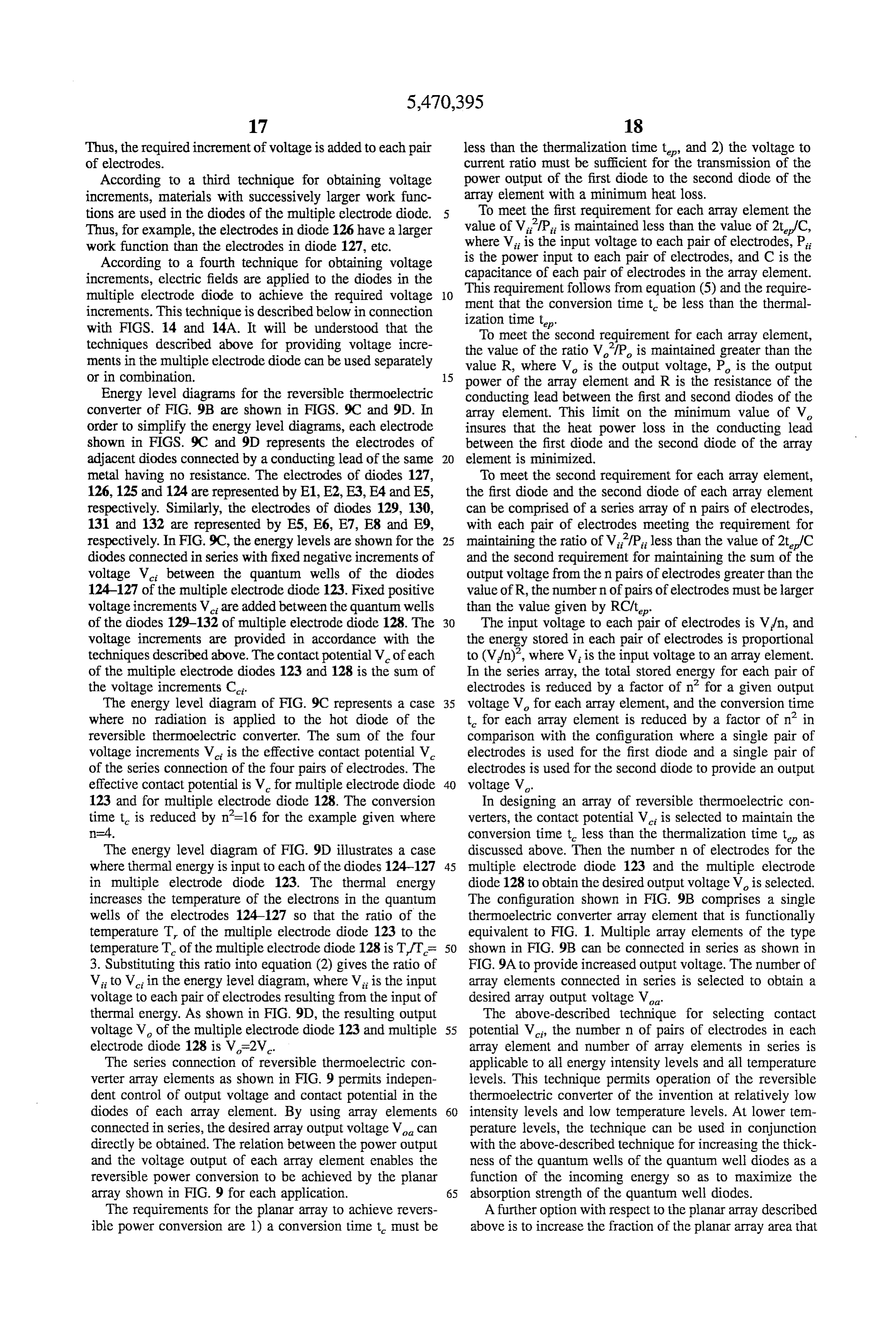
metal having no resistance. The electrodes of diodes 127, To meet the second requirement for each array element, 126,125 and 124 are represented by E1, E2, E3, E4 and E5, the first diode and the second diode of each array element respectively. Similarly, the electrodes of diodes 129, 130, can be comprised of a series array of n pairs of electrodes, 131 and 132 are represented by E5, E6, E7, E8 and E9, with each pair of electrodes meeting the requirement for respectively. In FIG. 9C, the energy levels are shown for the 25 maintaining the ratio of V/Pless than the value of 2t/C diodes connected in series with fixed negative increments of and the second requirement for maintaining the sum of the voltage V between the quantum wells of the diodes output voltage from then pairs of electrodes greater than the 124-127 of the multiple electrode diode 123. Fixed positive value of R, the number n of pairs of electrodes must be larger voltage increments V are added between the quantum wells than the value given by RC/t.
of the diodes 129-132 of multiple electrode diode 128. The 30 The input voltage to each pair of electrodes is V/n, and voltage increments are provided in accordance with the the energy stored in each pair of electrodes is proportional techniques described above. The contact potential Vof each to (V/n)', where V is the input voltage to an array element. of the multiple electrode diodes 123 and 128 is the sum of In the series array, the total stored energy for each pair of the voltage increments C. electrodes is reduced by a factor of n for a given output The energy level diagram of FIG. 9C represents a case 35 voltage V for each array element, and the conversion time where no radiation is applied to the hot diode of the t for each array element is reduced by a factor of n’ in reversible thermoelectric converter. The sum of the four comparison with the configuration where a single pair of voltage increments V is the effective contact potential V. electrodes is used for the first diode and a single pair of of the series connection of the four pairs of electrodes. The electrodes is used for the second diode to provide an output effective contact potential is V for multiple electrode diode 40 voltage V.
123 and for multiple electrode diode 128. The conversion In designing an array of reversible thermoelectric con time t is reduced by n=16 for the example given where verters, the contact potential V is selected to maintain the n=4. conversion time t less than the thermalization time t as The energy level diagram of FIG. 9D illustrates a case discussed above. Then the number n of electrodes for the where thermal energy is input to each of the diodes 124-127 45 multiple electrode diode 123 and the multiple electrode in multiple electrode diode 123. The thermal energy diode 128 to obtain the desired output voltage V is selected. increases the temperature of the electrons in the quantum The configuration shown in FIG. 9B comprises a single wells of the electrodes 124-127 so that the ratio of the thermoelectric converter array element that is functionally temperature T of the multiple electrode diode 123 to the equivalent to FIG. 1. Multiple array elements of the type temperature T of the multiple electrode diode 128 is T/T= 50 shown in FIG. 9B can be connected in series as shown in 3. Substituting this ratio into equation (2) gives the ratio of FIG. 9A to provide increased output voltage. The number of V to V in the energy level diagram, where V is the input array elements connected in series is selected to obtain a voltage to each pair of electrodes resulting from the input of desired array output voltage V.
thermal energy. As shown in FIG. 9D, the resulting output The above-described technique for selecting contact voltage V of the multiple electrode diode 123 and multiple 55 potential V, the number n of pairs of electrodes in each electrode diode 128 is V-2V. array element and number of array elements in series is The series connection of reversible thermoelectric con applicable to all energy intensity levels and all temperature verter array elements as shown in FIG. 9 permits indepen levels. This technique permits operation of the reversible dent control of output voltage and contact potential in the thermoelectric converter of the invention at relatively low diodes of each array element. By using array elements 60 intensity levels and low temperature levels. At lower tem connected in series, the desired array output voltage V can perature levels, the technique can be used in conjunction directly be obtained. The relation between the power output with the above-described technique for increasing the thick and the voltage output of each array element enables the ness of the quantum wells of the quantum well diodes as a reversible power conversion to be achieved by the planar function of the incoming energy so as to maximize the array shown in FIG. 9 for each application. 65 absorption strength of the quantum well diodes. The requirements for the planar array to achieve revers A further option with respect to the planar array described ible power conversion are 1) a conversion time t must be above is to increase the fraction of the planar array area that
Page 24
is used by the multiple electrode diode 123 (that corresponds angstrom evaporated aluminum oxide film and electrode 144 to diode 10 in FIG. 1). This is achieved by increasing the can be a 140 angstrom evaporated copper film. Terminal 154 contact potential increment V for the multiple electrode is typically connected to terminal 156. For this embodiment diode 128 (which corresponds to diode 20 in FIG. 1) up to of the invention, 1 kilowatt of output power is available per the limit established by the ratio of the input temperature T square centimeter of active area of the quantum well-diodes. to the cold reservoir temperature T. The ratio of the energy For both planar and nonplanar reversible thermoelectric stored in the multiple electrode diode 123 to the energy converter circuits, it is understood that layers can be used stored in the multiple electrode diode 128 is given by the over the top layer or under the bottom layer of the first diode temperature ratioTIT. The increase in the contact potential in the reversible thermoelectric converter circuit for con increment V up to the limit set by the ratio TT in turn 10 centration, antireflection or trapping of incoming solar establishes a limit of the ratio of the areas of the multiple energy, or for the conduction of circuit current. The radia electrode diode 123 to the area of the multiple electrode tion resistant and heat resistant common metals used in the diode 128. quantum wells of the reversible thermoelectric converter A second option with respect to the planar array is to circuit permit a wide selection of additional layers as to increase the output voltage V by increasing the number n of 15 shape, flexibility and texture. These options also include the pairs of electrodes without an increase in the output current use of minimum size solar concentrators, antireflection of the array element. The increase in the ratio of the output coatings and textured solar trapping cover glasses and voltage to the output current permits the multiple electrode substrates.
diodes 123 and 128 to be separated, while maintaining a The transparent conduction layers can include conduction minimum resistive loss. Thus, the multiple electrode diode 20 layers that can also function as antireflection coatings and 123 for receiving thermal energy for the power conversion trapping layers such as, for example, an indium tin oxide or heat pump process has maximum area at the receiving layer which can be added over the top electrodes of the first location. The configuration with separated hot and cold diode. Also, conduction and trapping layers can be added diodes is preferred in applications such as positioning the under the bottom electrodes of the first diode in the planar hot diode inside a furnace, and the cold diode outside the 25 array of FIG.9. When the conduction and trapping layer for furnace, or the hot diode on a home roof and the cold diode the nonplanar array is under the bottom electrode of the first inside the home. diode, the conduction layer functions as the barrier layer 148 A further option with respect to the planar array is to use shown in FIG. 10.
different numbers of pairs of electrodes in the hot multiple The conduction layers for trapping of incoming radiation electrode diode 123 and the cold multiple electrode diode 30 of any wavelength and intensity can meet the widest range 128 so as to transform the voltage-to-current ratio of the of applications and environments. In addition to the options input energy of the hot electrons to the required voltage-to for trapping, these options include options for maximizing current ratio of the output energy. This configuration can be the power conversion of a wide spectrum of intensities and used to transform the energy of optical photons incoming to wavelengths of incoming thermal radiation. the multiple electrode diode 123 to energy outgoing from the 35 One of these options is adding pairs of electrodes over the multiple electrode diode 128 with a voltage level ranging top electrodes and under the bottom electrodes of the first from below one millivolt to the electron voltage level of diode of the planar or nonplanar array elements, where the optical photons. added pairs of electrodes are connected in series and are A nonplanar reversible thermoelectric converter circuit is spaced by transparent conduction layers to provide addi shown in FIG. 10. In the nonplanar circuit, the quantum well 40 tional trapping path length. Each pair of electrodes has the diodes are fabricated in a vertical stacked array. A quantum required fixed increment of contact potential for the series well diode comprising electrode layers 136 and 138 sepa array, and each pair has the required thickness of the rated by a barrier layer 140 corresponds to diode 10 in FIG. quantum well for each electrode pair to provide the required 1. A quantum well diode comprising electrodes 142 and 144 absorption band.
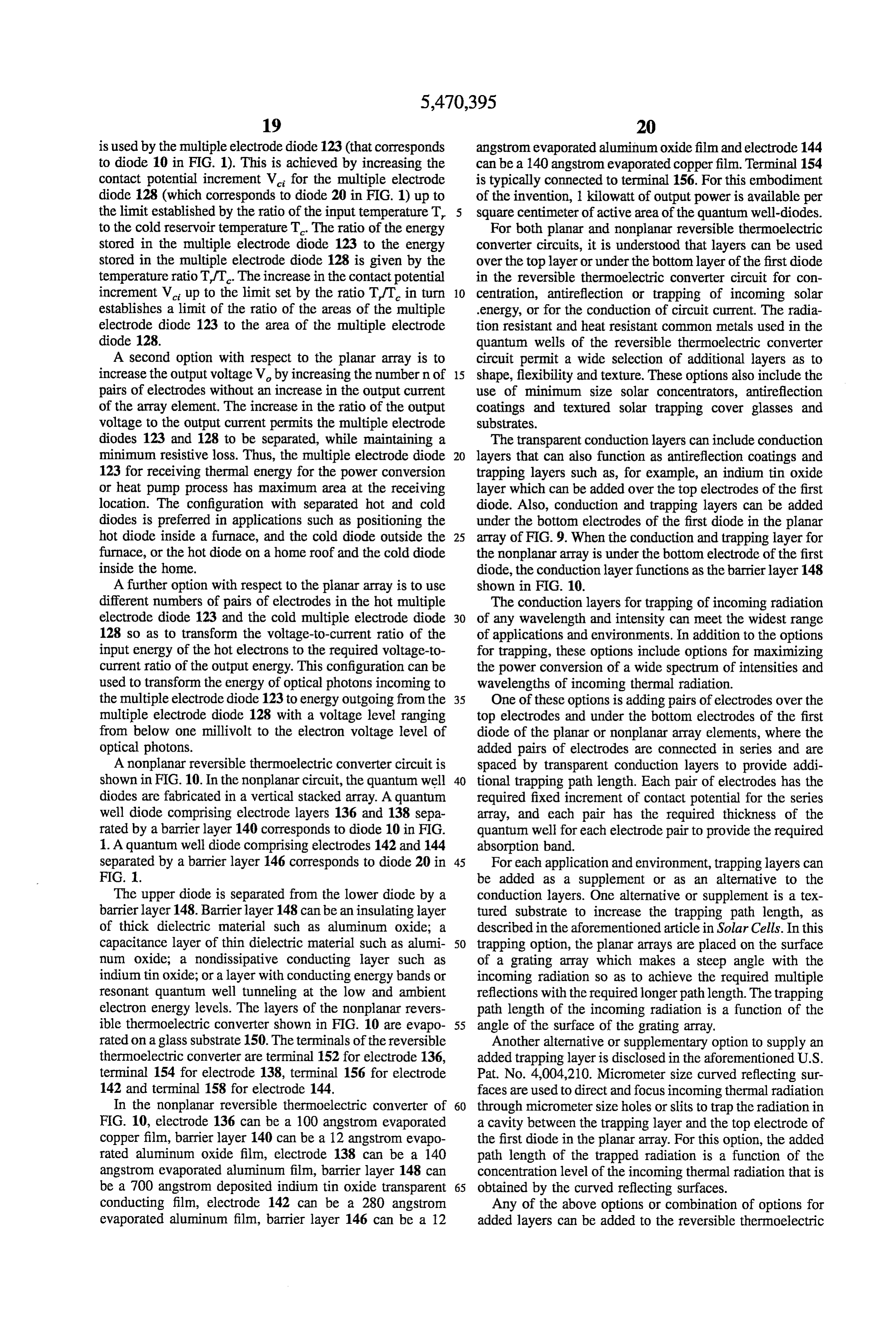
separated by a barrier layer 146 corresponds to diode 20 in 45 For each application and environment, trapping layers can FIG. 1. be added as a supplement or as an alternative to the The upper diode is separated from the lower diode by a conduction layers. One alternative or supplement is a tex barrier layer 148. Barrier layer 148 can be an insulating layer tured substrate to increase the trapping path length, as of thick dielectric material such as aluminum oxide; a described in the aforementioned article in Solar Cells. In this capacitance layer of thin dielectric material such as alumi 50 trapping option, the planar arrays are placed on the surface num oxide, a nondissipative conducting layer such as of a grating array which makes a steep angle with the indium tin oxide, or a layer with conducting energy bands or incoming radiation so as to achieve the required multiple resonant quantum well tunneling at the low and ambient reflections with the required longer path length. The trapping electron energy levels. The layers of the nonplanar revers path length of the incoming radiation is a function of the ible thermoelectric converter shown in FIG. 10 are evapo 55 angle of the surface of the grating array. rated on a glass substrate 150. The terminals of the reversible Another alternative or supplementary option to supply an thermoelectric converter are terminal 152 for electrode 136, added trapping layer is disclosed in the aforementioned U.S. terminal 154 for electrode 138, terminal 156 for electrode Pat. No. 4,004,210. Micrometer size curved reflecting sur 142 and terminal 158 for electrode 144. faces are used to direct and focus incoming thermal radiation In the nonplanar reversible thermoelectric converter of 60 through micrometer size holes or slits to trap the radiation in FIG. 10, electrode 136 can be a 100 angstrom evaporated a cavity between the trapping layer and the top electrode of copper film, barrier layer 140 can be a 12 angstrom evapo the first diode in the planar array. For this option, the added rated aluminum oxide film, electrode 138 can be a 140 path length of the trapped radiation is a function of the angstrom evaporated aluminum film, barrier layer 148 can concentration level of the incoming thermal radiation that is be a 700 angstrom deposited indium tin oxide transparent 65 obtained by the curved reflecting surfaces. conducting film, electrode 142 can be a 280 angstrom Any of the above options or combination of options for evaporated aluminum film, barrier layer 146 can be a 12 added layers can be added to the reversible thermoelectric
Page 25
converter circuit of the present invention. The requirements contact with the thermal reservoir for diode 20. The revers of the application and environment determine the options, if ible thermoelectric converter is protected by a multilayer any, needed to achieve the maximum performance. thermal conduction and convection shield comprised of An important application of the reversible thermoelectric closely-spaced thin film layers which are transparent to the converter is as an electro-optical amplifier. One embodiment incoming thermal radiation.
of this application is a two-stage amplifier in which a first In the furnace application, the heat sources have tempera stage serves to cool the input of a second stage as shown in tures in a range from 6000 K. down to temperatures below FIG. 11. A reversible thermoelectric converter includes 400 K. The design of the quantum well diodes for each second stage quantum well diodes 10 and 20 as shown in application must be in accordance with the design principles FIG. 1. A cooling stage includes quantum well diode 160 10 discussed above for different temperatures and intensity connected in parallel with diode 20 at terminal 22 by levels. The material and thickness of the electrodes of the conducting lead 162 and connected to terminal 164 by quantum well diodes are selected to provide quantum level conducting lead 166. The performance equations for the energy transitions for maximum oscillator strengths at the two-stage reversible thermoelectric converter show that as energy level of the incoming photons from the furnace. the effective input temperature of diode 20 is lowered by the 5 The protective thermal barrier, if needed for protection cooling stage, the gain of the second stage comprising from the environment, is a lightweight, thin film thermal diodes 10 and 20 is increased. The analysis shows a potential barrier layer designed to serve as a protective layer against gain in power of up to 40 dB for the two-stage reversible damage from the heat source. The thermal barrier is placed thermoelectric converter as the input temperature of diode to enable the reversible thermoelectric converter to intercept 20 is lowered to 60 K. The cooling stage, including diodes 20 the maximum amount of thermal energy at the highest 20 and 160 in FIG. 11, enables the two-stage amplifier to temperature from the heat source and to approach the amplify incoming energy that is below the noise level at maximum efficiency of the highest temperature, while main room temperature. taining the temperature of the cold diode at T=300°K. The The cooling stage also enables the amplifier circuit to protective shield intercepts negligible thermal heat on all obtain a 40 dB increase in the signal level so that signal 25 exposed surfaces other than the active area of diode 10 by levels below the noise level at room temperature can be the use of such reflective materials as the reflective layers amplified for signal levels and signal frequencies approach 120, 122 shown in FIG. 9.
ing that for an optical amplifier. To obtain this gain, a ratio In a first furnace embodiment, the reversible thermoelec of 100 must be maintained between the temperature of the tric converter is used at the highest temperature potentially hot electrons in diode 10 and the temperature of the cold 30 available from sources of thermal radiation, a solar furnace. electrons in diode 20. This ratio is obtained at a 60 K. A planar array, which can be fabricated in accordance with temperature of cold electrons in diode 20 when the electrons the above example for solar radiation, is coated with an in diode 10 are heated to a temperature of 6000 K. by oxide coating, such as aluminum oxide having a thickness of applied electrical energy or by incoming visible thermal 500 angstroms, to protect the array for extended periods. For radiation. To maintain this temperature for diode 20, diode 35 lower temperature ranges of 1000 K. to 2000 K., a thin 160 and diode 20 are operated as a heat pump so as to cool transparent film such as quartz can be used for protection. diode 20. The heat pump acts as a refrigerator device for When the reversible thermoelectric converter is operated diode 20. A DC current is applied from terminal 24 through in an AC mode within a thermal barrier enclosure, such as diode 20 and diode 160 to terminal 164. The power input to a furnace environment as described above, each diode the refrigeration cycle is given in part by the product of the 40 operates alternatively as a heat source and a heat sink for the input DC current and the contact potential V across diode other diode. Thus, a thermal reservoir is required for each 20. The other part of the power input to the refrigeration diode. The transported thermal energy is the same for the cycle is the heat energy input to diode 20 from the heat power conversion cycle from diode 10 to diode 20 and for reservoir in thermal contact with diode 20. For a refrigera the heat pump cycle from diode 20 to diode 10. The same tion cycle operating between the 300 K. temperature of 45 amount of heat is removed from the thermal reservoir of diode 160 and the 60 K. temperature of diode 20, the diode 20 during the heat pump cycle as the amount of energy coefficient of refrigeration performance for the reversible that is added to the thermal reservoir during the power thermoelectric converter is given by 60 K/(300 K.-60° conversion cycle.
K.) so that for this operating range, the coefficient of In order to provide high AC power output at low AC refrigeration performance is 1/4. The power input for the 50 frequencies, a larger thermal reservoir than that provided by heat pump P is given by P-4P, where P is the heat the electrodes of the quantum well diodes is required. The power required to be removed from diode 20. larger thermal reservoir can be metal layers contiguous to a One important group of applications of the reversible potential barrier that is deposited on the electrodes of the thermoelectric converter of the present invention is for quantum well diodes. These metal layers operate as a source power conversion where the heat source is fossil fuel, 55 and a sink for hot electrons in the heat pump cycle. nuclear, geothermal, waste heat, or any other fuel source. In An embodiment of a planar array of reversible thermo this case, the temperature of the immediate environment can electric converters having thermal reservoirs for the power approach the maximum temperature generated by the fuel. conversion process inside a thermally-insulated enclosure In general, these applications are referred to as furnace such as a furnace environment is shown in FIG. 12. Metal applications. The physical environment is such that the 60 strips 202, 203, 204 and 205 are deposited on a substrate reversible thermoelectric converter is located where the 210, which can be glass. The metal strips 202, 203, 204 and temperature is higher than room temperature T-300 K., 205 can, for example, be aluminum having a thickness in the where T is the temperature of the thermal reservoir for the range of 100 angstroms to 10 micrometers. The substrate cold diode 20. An example of the location of the reversible 210 is flexible and is supported in tension inside the thermal thermoelectric converter is in the wall of a furnace so as to 65 enclosure within the furnace to minimize heat loss by intercept the maximum amount of thermal radiation at the conduction. A potential barrier 212 is deposited over metal highest temperature, and also to maintain a close thermal strips 202, 203,204 and 205. The potential barrier 212 can,
Page 26
for example, be an aluminum oxide dielectric film having a A schematic diagram of a two-stage reversible thermo thickness of 10 angstroms. The remaining elements of the electric converter suitable for use in a furnace environment planar array are fabricated on potential barrier 212. The is shown in FIG. 13. It will be understood that each remainder of the planar array, including aluminum elec reversible thermoelectric converter is typically implemented trodes 102, 104 and 106, aluminum oxide barrier layer 110, as a planar array as described above. A reversible thermo copper electrodes 112 and 114, terminals 116 and 118 and electric converter comprising diodes 220 and 222 performs reflecting aluminum layers 120 and 122, has the same the power conversion function, and a reversible thermoelec configuration described above in connection with FIG. 9. tric converter comprising diodes 224 and 226 performs the The metal strips 202, 203, 204 and 205 are the thermal heat pump function. Diodes 220 and 222 are connected to reservoirs for the respective diodes of the planar array. The 10 output terminals 230 and 232, respectively, and are con potential barrier 212 allows the transfer of hot electrons to nected to each other via terminals 234 and 236. Diodes 224 and from electrodes 102, 104 and 106. The volume and and 226 are connected to output terminals 240 and 242, specific heat required for metal strips 202,203,204 and 205 respectively, and are connected to each other via terminals for a specific application are determined from the power 244 and 246. Power conversion terminals 230 and 232 output and the AC frequency. From the frequency and the 15 provide output power as described above. A DC source is power output, the amount of heat stored during the heat connected to terminals 240 and 242 to reverse the normal cycle is determined. As the thickness of the metal strips 202, direction of current flow through diodes 224 and 226. 203, 204 and 205 increases, the frequency of the AC power Diodes 222 and 224 are enclosed in a quasi-static heat conversion can be decreased to the range of commercial AC reservoir 250 at a temperature T, diode 220 is enclosed in transmission. 20 a quasi-static heat reservoir 252, and diode 226 is enclosed For AC operation within a thermal enclosure such as a in a quasi-static heatreservoir 254. Diodes 220, 222 and 224 furnace, some energy loss occurs during the fraction of the together with heat reservoirs 250 and 252 are enclosed power conversion-heat pump cycle that is used for operation within a quasi-static heat reservoir 256. of the heat pump cycle. The energy loss and the options for The heat reservoir 256 is the thermally-insulated enclo reducing such loss are a function of the AC frequency and 25 sure formed by thermal barriers and thermal shields inside the power output in each furnace environment. At the the furnace. The volume within the thermally-insulated highest AC conversion frequencies where the period of the enclosure acts as a quasi-static heat reservoir for operation AC conversion cycle and the circuit response time are less of the power conversion cycle of the reversible thermoelec than the electron thermalization time, all incoming energy is tric converter within the furnace. The wavelengths of inci converted into electric energy output during each AC period 30 dent thermal radiation absorbed by diode 220 are the only before any loss from electron thermalization occurs. There significant incoming or outgoing thermal heat to the interior fore, the maximum use of available energy in the furnace of the heat reservoir 256. Within the heatreservoir 256, heat environment is achieved. reservoir 252 operates as a heat reservoir for diode 220 The same result can be obtained for lower AC frequencies during the power conversion cycle. Heat reservoir 250 by reducing the fraction of the period of the AC conversion 35 operates as a heat reservoir for diodes 220 and 224 during cycle required for the heat pump cycle. By scaling the the power conversion and heat pump cycles. Heat reservoir dimensions of the electrodes or the current collection grid of 254, which is at the cool temperature of the output powerfor the quantum well diodes in an array of reversible thermo the power conversion-heat pump cycle, operates at the electric converters, the current capacity of the reversible output temperature T. The output temperature T of diode thermoelectric converter circuit can be increased by the 40 226 and the temperature T of the heat source for the amount needed to transport the thermal energy from diode incoming radiation determine the power conversion effi 20 during a short heat pump cycle needed to maintain the ciency for the power conversion cycle. temperature of diode 20 at the level of the outside cool In the furnace applications of the reversible thermoelec reservoir. Alternatively, mechanical, optical or electro-opti tric converter, resistive losses in the connecting leads can be cal techniques can be used to block absorption of the 45 significant. In order to minimize such losses, it is desirable incoming thermal radiation from the reversible thermoelec to minimize the length of conducting leads and to maximize tric converter during the brief intervals required for the heat the voltage generated by the reversible thermoelectric con pump cycle to remove thermal energy from diode 20. verter. The contact potential V of the quantum well diode is The available location within the furnace determines the a function of the different work functions of the materials size and shape of the power conversion reversible thermo 50 used in the electrodes. The output voltage of the reversible electric converter array. In one embodiment, two thin, ligh thermoelectric converter can be increased as shown in FIGS. weight, flat arrays are supported in tension, back-to-back by 9, 9A, 9B, 9C and 9D and described above. a thin supporting frame of a heat resistant material such as A series array of quantum well diodes having voltage tungsten. One array performs power conversion, and the increments added by an applied electric field is shown in other array acts as a heat pump. The reversible thermoelec 55 FIG. 14. An equivalent circuit diagram is shown in FIG. tric converter arrays are protected within a thermal enclosure 14A. The configuration shown in FIGS. 14 and 14A corre such that the temperature of the array approaches the maxi sponds to one of the multiple electrode diodes 123 or 128 mum temperature of the source while the arrays are ther shown in FIG. 9B and described above. mally protected against unusable convection heat by trans Auxiliary electrodes 270, 271 and 272 are deposited on parent, closely-spaced thin films in front of the active areas 60 glass substrate 108. A terminal 276 is in electrical contact of the quantum well diodes. The arrays are also thermally with electrode 270, and a terminal 278 is in electrical contact protected against unusable wavelengths of incoming thermal with electrode 272. The auxiliary electrodes 270, 271 and radiation using a thin layer that is closely spaced in front of 272 and terminals 276 and 278 can be an aluminum film 200 the active areas of the quantum well diodes. The thin layer angstroms thick. The planar array including electrodes 102, can be covered with a radiation absorbing metal film to 65 104,106, 112 and 114, dielectric layer 110 and terminals 116 convert the unusable wavelength of thermal radiation into a and 118, as described above in connection with FIG. 9, is usable wavelength. positioned over electrodes 270, 271 and 272. The planar
Page 27
array is separated from electrodes 270, 271, 272 by an planar array is given by the product of the total series insulating layer 274, which can be an aluminum oxide layer resistance times the total series capacitance of the n pairs of having a thickness of 500 angstroms. The electrodes 102, electrodes connected in series. The time constant is inde 104 and 106 are aligned with electrodes 270, 271 and 272, pendent of the number of array elements in the series planar respectively and preferably have the same dimensions. array, since the series resistance increases in proportion to A schematic diagram of the planar array of FIG. 14 is the number of pairs of electrodes, and the series capacitance shown in FIG. 14A. As discussed previously in connection decreases in proportion to the number of pairs of electrodes. with FIG. 9, electrodes 102, 104, 106, 112 and 114 define The time constant for the planar array circuit therefore series-connected diodes 280, 281, 282 and 283. A high reduces to the conversion time t for the reversible thermo impedance resistor 284 is connected between electrodes 271 10 electric converter as given by Equation (5), so that the value and 270, and a high impedance resistor 285 is connected oft can be maintained at a value less than 10' seconds. between electrodes 271 and 272. A voltage applied between In the second option, the n pairs of electrodes, each pair terminals 278 and 276 results in successively larger voltages with a capacitance C, are connected in series to terminals applied to electrodes 270, 271 and 272. Thus, equal incre 276 and 278 with a capacitance Co. between auxiliary ments of electric field are applied to diodes 280-283. The 15 electrodes 270 and 272 and electrodes 102 and 106, respec electrodes 102, 104, 106, 112 and 114 are typically of the tively, as shown in FIG. 14. The total sum of the voltage same metal, such as copper. The configuration shown in increments added to the pairs of electrodes is given by the FIGS. 14 and 14A represents one multiple electrode diode of ratio Co/(CohC/n) times the voltage applied between termi a reversible thermoelectric converter, such as diode 10 in nals 276 and 278. As a result of the fast response time with FIG. 1. A similar configuration is used for the second 20 maximum efficiency, together with the ultra light weight of multiple electrode diode of the reversible thermoelectric the planar arrays, the second option is preferred for the converter. Two multiple electrode diodes as shown in FIGS. power conversion of solar energy in space for applications 14 and 14A can be used to form an array element of a Such as the amplification and broadcasting of high frequency reversible thermoelectric converter. The array elements can power output for high definition television (HDTV) or for be connected in series as shown in FIG. 9A to obtain an 25 directed beams of output solar power or environmental data increased output voltage. using radio waves.
For applications where there is a requirement for time In the second option, as well as in all embodiments for varying voltage increments that are added by an applied adding varying voltage increments to the series arrays of electric field, the time constant of the RC circuit of the reversible thermoelectric converters, when the electrodes of auxiliary electrodes shown in FIGS. 14 and 14A can be 30 the series planar array are made of the same metal, with the varied to meet this requirement. As an alternative to a same Fermi level and the same work function, the polarity discrete component circuit, a high impedance resistive film of the contact potential V is reversed when the applied connected to terminals 276 and 278 can be used to replace electric field is reversed, resulting in a reversal of the output the auxiliary electrodes 270, 271 and 272 shown in FIG. 14 voltage Vo. Thus, an AC output voltage can be obtained, and the high impedance resistors 284 and 285 shown in FIG. 35 using any of the embodiments for adding varying increments 14A. The capacitance between each localized region of the of voltage to a series array, by a periodic reversal of the resistive film and the series planar array applies the electric voltage applied to terminals 276 and 278. field to add the voltage increments when a voltage is applied For applications of the second option to high frequency between terminals 276 and 278. output power or signals, two series arrays as shown in FIGS. To permit the resistive film RC circuit or the discrete 40 14 and 14A are connected as shown in FIG. 1 to form an component RC circuit of FIG. 14 to be used as one of the array element of a reversible thermoelectric converter. AC layers in the protective, trapping or antireflection layers on voltage inputs of opposite polarity at the required output the top of a series planar array, an insulating transparent frequency are applied to the terminals 276 and 278 of the protective layer such as aluminum oxide is deposited over two series arrays. The maximum amplitude of the AC the planar array. A transparent resistive film or a transparent 45 voltage input to terminals 276 and 278 for the two series discrete RC circuit is deposited over the transparent protec arrays is given by Equation (5) as the maximum value of Vo tive layer. The terminals for the transparent resistive film or for which the conversion time is less than the electron the transparent discrete component RC circuit are located thermalization time.
adjacent to terminals 116 and 118 and over electrodes 102 For applications of the second option to amplifying and 106, respectively. 50 incoming signals, a DC voltage is applied between terminals In a second option having the lowest RC time constant 276 and 278. The DC voltage meets the same condition for using a capacitance circuit, the voltage increments are the maximum value given by Equation (5) for Vo for the obtained by an applied electric field which adds a voltage amplified output voltage of the maximum incoming signal. increment to each electrode pair that is inversely propor The DC voltage is used as the applied input voltage to tional to the capacitance across each quantum well electrode 55 terminals 276 and 278 of the first and second multiple pair. In the second option of the series planar array, the electrode diodes of a reversible thermoelectric converter. auxiliary electrodes 270 and 272 and the terminals 276 and The incoming AC signal is applied to terminals 276 and 278 278 are used. The voltage applied between terminais 276 of the cold first multiple electrode diode attemperature T. and 278 is capacitively coupled by auxiliary electrodes 270 The Solar energy is incident on the hot second multiple and 272 to electrodes 102 and 106, respectively, of the 60 electrode diode at temperature T.
planar array. For an extended series and parallel connection of revers In the second option, with the auxiliary electrodes on ible thermoelectric converter array elements, each com either the top layer or the bottom layer of the planar array, prised of first and second multiple electrode diodes as shown the response time to the voltage that is applied between in FIGS. 14 and 14A, a desired output voltage can be terminals 276 and 278 can be as short as the response time 65 obtained from the series connection of array elements and a of the reversible thermoelectric converter of the present desired output current can be obtained from the parallel invention. The time constant of each option of the series connection of array elements. For an extended array in
Page 28
which the intensity and temperature of the input thermal thermal radiation in the high temperature band. Diode 224, energy are varying with time over the area of the total planar which converts the lower temperature band, is in close array, the voltage applied to each section of the array can be thermal contact with diode 220 and uses a series planar array varied as required to achieve optimum performance for each of electrodes designed for the lower temperature range. section of the array. Diode 224 can also include thermal reservoirs for the power Also, optimum performance can be achieved for each conversion process, corresponding to metal strips 202-205 Section of the planar array using variable applied voltage to in FIG. 12, and has a series planar array of electrodes for control the contact potential in the planar array structure of adding voltage increments corresponding to that shown, for FIG. 9. A transparent auxiliary electrode is affixed to the top example, in FIG. 14. The use of thermal reservoirs allows of the planar array, and an auxiliary electrode is affixed to the 10 the reversible transfer of hot electrons to and from the bottom of the planar array shown in FIG. 9. In this configu electrodes of diode 220 and the electrodes of diode 224. The ration, the reflecting layers 120 and 122 and the electrodes ability to vary voltage increments applied to the series array, are fabricated of the same metal, and the contact potential of corresponding to that shown in FIG. 14, permits the perfor the array element corresponds to the voltage applied mance of the two-stage reversible thermoelectric converter between the auxiliary electrodes. 5 for a power conversion-heat pump cycle or for a dual For each section of an array using planar arrays as shown thermal band power conversion cycle to be optimized. The in FIGS. 14 and 14A and described above, the application of option to generate AC output power can be used in the a varying voltage between the terminals 276 and 278 permits furnace environment for transmission of conversion energy the total contact potential of n pairs of electrodes to be varied outside the furnace environment, using either thermally in proportion to the applied voltage. Also, for each section 20 insulated conducting leads or capacitive coupling of the of an array using the planar array structure shown in FIG.9 conversion energy between heat reservoirs. in which the workfunction of each electrode is the same, the The planar array of reversible thermoelectric converters application of a varying voltage between auxiliary elec of the present invention can be utilized in a lightweight, trodes above and below the planar array permits the contact highly efficient space module array for solar energy conver potential for each diode of the array section to be varied in 25 sion or as an amplifier. For the space environment, no proportion to the applied voltage. thermal insulation of the space module array is required, For all of the array embodiments using electrodes fabri except for the nonactive surfaces that are exposed to direct cated of the same metal, AC output power can be obtained sunlight. The absorption of solar energy by the nonactive without storing thermal energy during the AC cycle. surfaces is minimized by a reflective surface coating such as The variable contact potential options described above are 30 aluminum. The low temperature space environment enables in addition to the fixed contact potential options, such as the power conversion-heat pump thermodynamic cycle for obtained by the use of implanted ions or metal alloys. The the reversible thermoelectric converter to be operated near fixed increments of contact potential are used for applica maximum efficiency. The incident solar energy that is tions that do not require variable applied contact potential. absorbed by the nonactive area of the array is very small, and Examples of applications of variable applied contact poten 35 the power loss due to the incremental change in temperature tial are to vary the contact potential V as a function of is not a significant factor in the power output. Planar arrays varying temperature and/or intensity of the input thermal of reversible thermoelectric converters with a thin film energy, or to vary the contact potential V to obtain AC construction can be supported with a lightweight structure output power without storing thermal energy during the AC and can be unfurled in space. The ultra light weight of the cycle. 40 space module array is evident from the fact that the weight In the furnace application, the cool diode of the reversible of a 100 square meter space array, including supporting thermoelectric converter can be separated from the hot booms, can be as little as 10 kilograms, as described by J. C. diode, so that the hot diode is located on the inside surface Yater in Applied Optics, February 1975, pages 526-536, in of the furnace wall and the cool diode is located outside the connection with supporting a film of similar size in syn furnace in thermal contact with the cold heat reservoir. This 45 chronous orbit. The three millimeter diameter quartz booms separation is achieved by increasing the voltage to current supporting one square meter panels of arrays have a bending ratio of the series array as described above. For example, moment well below the critical bending moment. At this with reference to FIG. 13, where diodes 224 and 226 remove diameter, the ratio of boom weight to array weight is small. power conversion heat loss from diode 222, diode 226 can The space support structure for the thin film planar arrays be removed from the furnace environment to a cold reser 50 can be several orders of magnitude lighter than the support voir. In a similar manner, diodes 222 and 226 can be structure for a comparable thin film planar array on Earth. removed from the furnace environment, and diode 224 can For a space structure using 100 rows of 100 panels, each of be placed in close thermal contact with diode 220 so as to one square meter, the total power can be larger than 10 operate either in a power conversion-heat pump cycle or in megawatts. The weight of the square space array can be as a dual thermal band power conversion cycle. This configu 55 little as 20 kilograms, not including the weight required for ration is used for obtaining maximum efficiency and/or the interconnection as a power relay of solar energy or as a maximum power output for the power conversion cycle. power source for signal relay of digital high definition TV Operating in the heat pump cycle, the diode 224 improves signals.
power conversion performance by lowering the temperature A second embodiment of the space module uses a two of diode 220. Operating in the dual thermal band power 60 stage reversible thermoelectric converter as shown in FIG. conversion cycle, diode 224 improves power conversion 13, which can operate reversibly using little or no concen performance by increasing available power output for a tration of solar energy. In this case, the space module second lower temperature band of incoming heat through comprises three submicrometer thick substrates supported in heat reservoir 256. For the dual thermal band power con tension by millimeter diameter booms. The first substrate versions cycle, diode 220, which converts the high tempera 65 supports the series array first diode corresponding to diode ture heat band, uses series array electrodes of high tempera 220 in FIG. 13. The second substrate is in thermal contact ture metals such as tungsten to intercept all the incoming with the first substrate and supports both the series array
Page 29
second diode corresponding to diode 222 in FIG. 13 and the operation of the power conversion-heat pump cycle shown cold series array first diode of the heat pump corresponding in FIG. 15 are an AC signal control and a DC signal control to diode 224 in FIG. 13. connected in series with the output of the panel array. The The third substrate is not in thermal contact with the AC signal control delivers the power required to reverse the second substrate and supports the series array second diode output current direction. The AC and DC controls allocate a of the heat pump cycle corresponding to diode 226 in FIG. portion or all of the power to DC power such as for storage 13. The inner surface of the third substrate has a thermally of DC power.
reflective layer adjacent to the second substrate and has a The planar array and the power conversion-heat pump thermally emissive layer on the outer surface so as to operate cycles of the reversible thermoelectric converter of the as the heat reservoir for the series array second diode of the 10 present invention have applications for the energy needs of heat pump cycle. the home. In one option, the planar arrays mounted in panels Using DC power from the power conversion cycle, the on the home roof as shown in FIG. 13 can comprise only the heat pump cycle operates between the cryogenic tempera first diode (diode 10, FIG. 1) of the reversible thermoelectric converter. The planar array second diode (diode 20, FIG. 1) ture of the second substrate and the temperature of the third is placed in a separate location to enable the power conver substrate of approximately 160 K. The Carnot efficiency 5 sion heat loss to be directed inside the home when needed limit for this power conversion-heat pump cycle of the for heat or to be directed outside the home when not needed intercepted solar energy is 97%. The operation of the revers for heat. When the first and second diodes are separated, the ible power conversion-heat pump cycle using components at ACneeds of the home can be obtained by operating with AC cryogenic temperatures minimizes heat losses, including power output, without storing heat energy during the AC transmission losses of the output power. 20 cycle. When there is no solar energy input, the roof first Either of the power conversion space modules described diodes and the second diodes can be operated in the heat above can be used by attaching the power conversion space pump cycle for air conditioning in warm weather, or as a module to the two-stage amplifier shown in FIG. 11 for heat pump in cold weather, operation in a combined power conversion-amplifier cycle The two-stage reversible thermoelectric converter shown to broadcast radio waves, such as HDTV signals. Preferably, 25 in FIG. 13 and described above can be used in the hone the two-stage space module corresponding to FIG. 13 is configuration. The heat pump function is performed by used. Signals received by a dipole filament array antenna are diode 224 in FIG. 13 operating in thermal contact with the applied between terminals 22 and 24 of diode 20 of the second diode of the home roof configuration. The diode two-stage amplifier shown in FIG. 11. The received radio corresponding to diode 224 is positioned to transport ther wave signals are amplified using solar energy input to heat 30 mal energy to the inside of the home. The two-stage revers the electrons in diode 10 to a temperature of 6000 K. Also, ible thermoelectric converter can also be operated to cool the the input DC power from the two-stage space module output second diode of the home roof power conversion configu terminals, corresponding to terminals 230 and 232 in FIG. ration to the low temperature that is required in the power 13, is applied to terminals 24 and 164 of the two-stage conversion-heat pump cycle. The two-stage reversible ther amplifier shown in FIG. 11 to cool diode 20. 35 moelectric converter can also be used to help maintain The amplified received signal at output terminals 14 and power conversion as the solar intensity decreases. 24 of the two-stage amplifier shown in FIG. 11 is applied An application of the reversible thermoelectric converter between terminals corresponding to terminals 276 and 278 of the present invention in heating and air conditioning ducts of the series array first diode shown in FIG. 14, wherein the is shown in FIGS. 16A and 16B. Insulated ducts 330 and 332 planar array first diode corresponding to diode 220 in FIG. 40 run side-by-side with one duct carrying heated air and the 13 is implemented as shown in FIG. 14. Also, an amplified other duct carrying cooled air. Openings are formed inducts received signal of equal amplitude and opposite polarity is 330 and 332, and a reversible thermoelectric converter applied between the terminals corresponding to terminals assembly is mounted between the ducts. Quantum well 276 and 278 of a separate planar array second diode, also diode arrays 334 are mounted within duct 332, and quantum implemented as shown in FIG. 14. The planar array second 45 well diode arrays 336 are mounted within duct 330. Diode diode corresponding to diode 222 in FIG. 13 is implemented array 334 corresponds to diode 10 in FIG. 1, and diode array as shown in FIG. 14. The applied signal modulates the AC 336 corresponds to diode 20. The diode arrays are fabricated waveform of the space module output power delivered on substrates 338 which can be flexible films of glass or between output terminals corresponding to output terminals quartz. The diode arrays 334 and 336 are mounted in slots 230 and 232 in FIG. 13. The output power is delivered to a 50 in a plastic or ceramic support frame 340 positioned between transmitting antenna, such as a dipole filament array air ducts 330 and 332. The diode arrays 334 and 336 are antenna. The transmitted signal can be the combined power clamped in position by metal contacts 342 attached to output of an array of one square meter space modules. support frame 340. Outer surfaces 344 of support frame 340 An application of the reversible thermoelectric converter facing air ducts 330 and 332 are coated with a thermal of the present invention for power conversion and heat pump 55 reflector such as aluminum. Diode arrays 334 and 336 are cycles is shown in FIG. 15. Panels 302, each comprising connected in series by conducting leads 346 and 348 in the planar arrays of reversible thermoelectric converters with a configuration shown in FIG. 1 and are connected to output series/parallel configuration as described above, are terminals 350 and 352.
mounted on a roof 304 of a home 306. The panels 302 are For the reversible thermoelectric converter of the inven mounted by steel wires 308 connected to brackets 310 60 tion operating in the heat pump cycle, the first and second attached to roof 304. A power output cable 312 is connected diodes can comprise n pairs of electrodes as described above to a distribution box 314 and to a power storage means 316. in connection with FIGS. 9-9D., 14 and 14A. The ability to Each panel 302 contains a power conversion-heat pump operate at low heat intensity and low temperatures, the module comprising planar arrays of reversible thermoelec ability to separate the first and second diodes of the heat tric converter circuits. The output voltage is 120 volts, and 65 pump, and the ability to utilize the various array configu the maximum power output is on the order of several rations described above can be applied to the heat pump hundred watts. The only additional items required for the configurations.
Page 30
The heat pump configuration can be utilized in automo of FIG. 13, is placed on top of diode 226. Diode 226 is biles. In this case, a series array first diode is mounted in the mounted on substrate 338 and in close thermal contact with upholstery of the seats and/or the ceiling of the automobile, diode array 336.
and the series array second diode is placed in an area of the The planar arrays Of the two-stage configuration as automobile exposed to the outside air. This configuration can applied to FIG. 16A can utilize the diode array shown in be used to heat or cool the automobile efficiently. FIG. 14. The terminals 276 and 278 in the array of FIG. 14 The configuration shown in FIGS. 16A and 16B can also are used for applying an external electric field to add be utilized in the power conversion of thermal energy in a incremental increase in contact potential for successive pairs high temperature or furnace environment. For this applica of electrodes. The terminals 116 and 118 of the planar array tion, the required number of pairs of electrodes for the diode 10 of FIG. 14 correspond to terminals 350 and 352 in FIG.16A. array 334 and the required number of pairs of electrodes for In the two-stage reversible thermoelectric converter, con the diode array 336 are selected to permit separation of diode ducting leads 350 and 352 are replaced with multiple leads arrays 334 and 336, while minimizing the dissipative ther including conducting leads for each of the diodes and mal conduction loss. Insulated duct332 carries unheated gas conducting leads for applying an external electric field to inside the transparent wall of duct 332 facing diode array 15 each of the array elements.
334. The walls of duct332 can be of quartz film spaced from In the two-stage reversible thermoelectric converter, the diode array 334 to permit air flow for cooling of the diode arrays corresponding to diodes 224 and 226 in FIG. 13 transparent film and diode array 334. The duct 330 is a rigid are operated in the heat pump cycle to remove the small non-transparent duct carrying cooled gas or cooled liquid for incoming leakage heat so as to achieve maximum conver removing power conversion heat loss so as to maintain a 20 sion efficiency from diode arrays 334 and 336. When the cool temperature of the diode array 336. Either AC or DC incoming heat is at a lower temperature, the diode array 224 operation can be utilized. The AC output can be transported of FIG. 13 is operated in a lower temperature power con over longer distances by using step-up transformers at the version cycle. The dual ranges for the temperature and output of terminals 350 and 352. power outputs are obtained by controlling the contact poten When cooling gas flow is not utilized in duct 332, the 25 tial V and the output voltage so as to maximize the power diode array 334 can be constructed of high temperature output. For both power conversion cycles, an AC output can material, such as tungsten for the metal electrodes and be used to supplement the power output from inside the aluminum oxide for the substrate. For operation between the furnace environment so as to minimize thermal conduction temperature of the source of incoming radiation and the cold losses.
temperature of diode array 336, there are no dissipative heat 30 In summary, the physical basis for the reversible process losses in diode array 334. of the reversible thermoelectric conversion invention is that The rate of incoming heat conduction to diode array 334 the conversion time of the thermal energy of the incoming can be minimized by using spaced layers of quartz material hot electrons is smaller than the thermalization time t for for the transparent wall of duct 332 facing diode array 334. the hot electrons. This result is achieved by limiting the The equilibrium temperature of the crystal lattice in diode 35 storage time for the electromagnetic energy in the energy array 334 is thereby minimized so that a moderate tempera levels of the quantum well electrodes so as to thereby limit ture is maintained. The equilibrium temperature depends on the conversion time.
thermal equilibrium for the radiation of the metal electrode This is achieved by reducing the level of the voltage input crystal lattice in the direction back to the heat source being V generated by the conversion of the thermal energy input equal to the heat conduction through the transparent wall of 40 of the hot electrons, by limiting the contact potential V for duct 332 facing diode array 334. An increase in the voltage the quantum well electrodes. The limit for V is a function to current ratio by increasing the number n of electrode pairs of the incoming power rate, the capacitance between the in diode array 334 enables the heat loss by thermal conduc quantum well electrodes, the ratio of the temperature of the tion through conducting leads 346 and 348 to be minimized. hotelectrons to the temperature of the cold electrons, and the To further decrease and minimize heat conduction loss 45 thermalization time of the hot electrons. through conducting leads 346 and 348, the power conver The physical basis of the reversible process of the revers sion output can be a high frequency AC power output that is ible thermoelectric conversion invention which enables the transmitted through capacitors that replace conducting leads first diode to be separated from the second diode of the 346 and 348. conversion circuit by the distance required for each appli The configuration shown in FIGS. 16A and 16B can be 50 cation and environment is that each first diode and each used in a variety of furnace and high temperature environ second diode can be comprised of a series array of pairs of ments including spatially distributed heat sources and heat electrodes as shown in FIG. 9B. For this series array, the sources that vary in temperature and intensity. For example, contact potential between each pair of electrodes can be in the power conversion application where cooling gas flow added in series with the series sum the same for the resultant is not used and where the maximum power output is required 55 contact potential for the first diode and the second diode. The for a high temperature turbulent environment with varying resultant contact potentials V for the series array of pairs of temperature bands, a two-stage reversible thermoelectric electrodes in the reversible thermoelectric conversion circuit converter can be used to provide increased output by utiliz can be increased so as to give the voltage output V, which ing a power conversion-heat pump process or by utilizing a is required to transport the conversion energy from the first dual thermal band power conversion cycle. 60 diode over the required separation distance to the second A two-stage reversible thermoelectric converter as shown diode.
in FIG. 13 can be used for high capacity output when Examples of the options for adding the increments of mounted on substrates 338 in FIG. 16A. For high capacity contact potential V to the series array of electrode pairs are use, diode array 334, which corresponds to diode 220 in given above for both fixed increments and variable incre FIG. 13, is placed on top of diode 224 of FIG. 13. Diode 224 65 ments of voltage. For each option, as shown in the energy is mounted on substrate 338 and in close thermal contact level diagram of FIG. 9C, the Fermi levels become equal for with diode 334. Diode 336, which corresponds to diode 222 the equilibrium state after contact is made between all pairs
Page 31
of electrodes for the reversible thermoelectric circuit. After time varying contact potential can be achieved for the the equilibrium state shown in FIG.9C is established for the reversible thermoelectric conversion circuit. typical ultrafast conversion circuit, it can be seen from FIG. The physical basis of the reversible process which enables 9C that the pairs of electrodes represented by E1 to E4 and the electrical energy from the power conversion, heat pump, E6 to E9 are equivalent electrically to two diodes. These two or refrigeration cycle, or combined cycles, to be transported equivalent diodes are able to function as one first diode and between the first and second diodes over extreme distances, one second diode with each diode having an effective as in geothermal or space power conversion or over extreme contact potential V equal to the sum of the contact poten temperature differences, as from incandescent to cryogenic tials V of these 4 pairs of electrodes. As a result, by temperatures, is that the use of reversible auxiliary compo increasing the number n of pairs of electrodes in series for O nents together with the use of the input voltage waveform the first diode and the second diode as required to achieve required for the transportation of the electrical energy the required output voltage, the separation distance between between the first and second diodes, enables the perfor the first diode and the second diode can be increased to meet mance of the reversible thermoelectric conversion cycles of the requirements of all the major applications. this invention to be achieved.
The performance output of the reversible thermoelectric 15 To achieve the required input waveforms, an AC electric conversion circuit is a function of the resultant contact field is used to apply a variable AC contact potential to the potentials V of the sum of the contact potentials of the series array of pairs of electrodes for the first and second series array whereas, the conversion time for each incoming diodes as described above. For each diode, as shown in FIG. hot electron input is a function of the contact potential V. 14, auxiliary electrodes 270 and 272 connected to terminals of only one pair of quantum well electrodes in the series 276 and 278, can be used to apply the AC contact potential array for the first diode. As a result, both the conversion time by capacitance coupling to the first and last electrodes, 102 and the output voltage of the reversible thermoelectric and 106, of the series array for both the first and second conversion circuit can be achieved independently so as to diodes. The required Voltage level for the AC waveforms for meet the requirements for each of the major applications. the transportation of the conversion energy in each direction The physical basis of the reversible process of the revers 25 between the first and second diodes is obtained by the use of ible thermoelectric conversion invention which enables an two voltage transformers.
applied electric field to add a variable contact potential in The primary terminals of each step up transformer are series between each pair of electrodes in the series array of connected to the terminals 16 and 118 of each series array pairs of electrodes is comprised of two combined reversible as shown in FIG. 14. One of the secondary terminals of each processes. In one of the reversible processes, the energy of 30 step up transformer is connected to the connecting lead the resultant electrostatic field between the pairs of elec between the first and second diodes, and the other secondary trodes is minimized and, in the second of the reversible terminal of each step up transformer is connected to the processes, the equilibrium for the chemical potential of the output lead of the reversible thermoelectric converter. The reversible thermoelectric conversion circuit is established. voltage level of the AC waveform for the electrical energy In the first of the reversible processes, the electric field is 35 output from the first and second diodes is increased by the applied by auxiliary electrodes and the energy of the elec step up transformer up to the voltage level required for trostatic field between the pairs of electrodes is minimized, minimizing all transmission losses between the first and in accordance with Thompson's Theoren, by the separate Second diodes. For applications such as for the geothermal distribution of charges on the surface of each auxiliary energy conversion at maximum depth and temperature, the electrode and each pair of quantum well electrodes. This 40 use of transparent heat reservoir to enclose the first diode charge distribution occurs within the minimum response and connected step up transformer, such as described above time for the capacitance of each electrode pair and generates using spaced layers of quartz material, can enable the the contact potential V for each electrode pair that is equilibrium temperature inside the heat reservoir, for the inversely proportional to the capacitance of each electrode crystal lattice of the first diode and the conducting wire of pair. Each contact potential V represents the added positive 45 the connected step up transformer, to be minimized so that or negative voltage to each electrode that increases or the reversible conversion processes of the first diode and the decreases the voltage potential level of each succeeding connected step transformer can be achieved without the use electrode pair in the applied electric field. of coolant flow or added heat pump processes. The second of the combined reversible processes estab Similar increased separation distances for transporting lishes the equilibrium for the chemical potential of the Fermi 50 thermal energy from the second diode to the first diode can Dirac distribution in the reversible thermoelectric conver be achieved by this reversible process for the heat pump or sion circuit and also in the ultrafast time for a typical refrigeration cycles. To further increase this temperature application. Equilibrium for the chemical potentiai, which, range for the power conversion cycle, the thermal heat for the Fermi Dirac distribution, is equal to the Fermi energy, reservoirs for the second diode can be used to alternatively gives the result that the Fermi level has a constant value for 55 store and then remove the power conversion loss by using a all Fermi conductors in the reversible thermoelectric con heat pump cycle for the second diode during the AC cycle version circuit so that the levels must be equal for all pairs for which a DC component is added to the AC waveform for of quantum well electrodes that are in contact. additional cooling of the second diode. The energy level diagram for the final result of these two A basic option to achieve the required reversible perfor combined reversible processes is shown in FIG. 9C. As 60 mance from the voltage transformers for the power conver shown, the first reversible process establishes the contact sion cycle from a hot environment is the combined revers potential V of these 8 pairs of electrodes for the reversible ible cycle option shown in FIG. 13 with diodes 224 and 226 thermoelectric circuit represented by FIG.9C. The result of operating in a heat pump cycle to lower the temperature of the second reversible process as shown establishes the equal diode 220 where the first diode 220 and the second diode Fermi level of all the pairs of electrodes for the reversible 65 222 can operate in a power conversion cycle with diodes 222 thermoelectric circuit represented by FIG.9C. As a result of and 226 being located in cool temperature reservoirs outside these two processes that, typically, can both be ultrafast, a the hot environment. This combined cycle can maintain the
Page 32
temperature of the quasi-static heat reservoir 252 enclosing than the external source, comprising: first diode 220 at the lower temperature required for revers a first device comprising first and second regions wherein ible power conversion without any loss in the overall electric carriers are quantized in discrete energy levels, efficiency. For this option, the step up transformer is placed and a third region providing a potential barrier between within the quasi-static heat reservoir 252 and with the said first and second regions, said first device receiving temperature maintained as low as required to transform the thermal energy from the external source and converting voltage reversibly, using superconduction operation for the the thermal energy into electric voltage fluctuations; transformers if required. This example of an option for the a second device comprising first and second regions control of the environment for auxiliary state-of-the-art wherein electric carriers are quantized in discrete components is an example of achieving a practical reversible 0 energy levels, and a third region providing a potential process for many applications of the reversible thermoelec barrier between said first and second regions, said tric converter.
Additional reversible auxiliary components that can be second device converting electric voltage fluctuations placed in the connecting leads between the first and second to thermal energy at a higher temperature than the diode are capacitors. One application for the series connec 15 means temperature of the external source; tion of coupling capacitors to the connecting leads is to for supplying to said first device a DC voltage reduce the energy loss by thermal conduction through the sufficient to reverse a contact potential across said first conducting leads in regions of high thermal gradients such device; and as in the high temperature region close to the first diode. For means for electrically connecting said first device to said the refrigeration cycle approaching that for cryogenic tem second device without a thermal barrier between them peratures, these regions can be close to the second diodes. 20 such that the electric voltage fluctuations generated by The protection afforded by the capacitors against thermal said first device in response to energy fluctuations from loss for extreme temperature gradients can be used alone or said external source are coupled to said second device together with the transformers in the connecting leads for and are converted by said second device to thermal high to low temperature applications involving supercon energy at a higher temperature than the temperature of ducting materials. 25 said external source.
One example of the combined use of capacitors to protect against thermal loss and transformers to protect against second devices as 2. Apparatus defined in claim 1 wherein said first and each comprise quantum well diodes.
resistance loss is based on adding the use of the coupling 3. Apparatus as defined in claim 1 wherein the first and capacitor to the above example of the combined reversible second regions of said first device and said second device power conversion-heat pump cycle shown in FIG. 13. For 30 comprise electrode pairs and said first device comprises two this example, the coupling capacitor is placed in the thermal insulating wall of the heat reservoir, the outside capacitor or more electrode pairs connected in series and said second terminal is connected through the conducting lead to the device comprises two or more electrode pairs connected in second diode and the inside capacitor terminal is connected series.
to the high voltage output terminal of the step up voltage 4. Apparatus as defined in claim 1 wherein said first and transformer. The combined two stage reversible thermoelec 35 second devices each comprise tunnel diodes. tric converter uses the reversible step up transformer to 5. Apparatus as defined in claim 1 wherein said first and minimize the electrical power loss in transmitting electrical second regions each comprise thin metal films and said third power between the first and second diodes and uses the region comprises a thin dielectric film, said first and second reversible coupling capacitor to minimize the thermal power devices each further including means for applying a contact loss in transmitting electrical power between the inside and 40 potential between the metal films of said first and second the outside of the thermal insulating wall of the cold heat regions.
reservoir inside the furnace. This reversible performance can 6. Apparatus as defined in claim 1 wherein said first and be obtained for the maximum power output that is generated second regions each comprise thin metal films and said third inside the highest temperature furnace and that is transmitted region comprises a thin dielectric film, said first and second for reversible power conversion to the cold second diode 45 devices each further including auxiliary electrodes for over the separation distance between the first and second applying an electric field between the metal films of said first diodes. This performance can be achieved using state-of and second regions.
the-art auxiliary components by controlling the environment 7. Apparatus as defined in claim 1 wherein the first region inside the heat reservoirs enclosing the auxiliary compo of said first and second devices comprises a first thin metal letS. 50 film, wherein the second region of said first and second Therefore, since the transformer and capacitors are devices comprises a second thin metal film and the third reversible components in this controlled environment, these region of said first and second devices comprises a thin components, as well as other reversible components or dielectric film, said first and second thin metal films being combinations of reversible components in a controlled envi fabricated of metals with different work functions. ronment, can be used in circuits connected to the reversible 55 8. Apparatus as defined in claim 1 wherein the first region thermoelectric converter of this invention, while accom of said first and second devices comprises a first thin metal plishing the reversible processes inherent to the reversible film, wherein the second region of said first and second thermoelectric processes of this invention. devices comprises a second thin metal film and the third While there have been shown and described what are at region of said first and second devices comprises a thin present considered the preferred embodiments of the present 60 dielectric film, said first and second thin metal films being invention, it will be obvious to those skilled in the art that fabricated of metals with the same work function. various changes and modifications may be made therein 9. Apparatus as defined in claim 1 wherein the first region without departing from the scope of the invention as defined of said first and second devices comprises a thin aluminum by the appended claims. film, the second region of said first and second devices What is claimed is: 65 comprises a thin copper film and the third region of said first 1. Apparatus for converting thermal energy from an and second devices comprises a thin aluminum oxide film. external source to thermal energy at a higher temperature 10. Apparatus as defined in claim 1 wherein the first
Page 33
region of said first and second devices comprises a thin for supplying to the third quantum well diode a DC copper film, the second region of said first and second voltage sufficient to reverse the contact potential across devices comprises a thin copper film and the third region of the third quantum well diode, and means for electri said first and second devices comprises a thin aluminum cally connecting the third quantum well diode to the oxide film. fourth quantum well diode without a thermal barrier 11. Apparatus as defined in claim 3 wherein said means between them such that electric voltage fluctuations for electrically connecting said first device to said second generated by the third quantum well diode are coupled device comprises a conducting lead, wherein the electrical to the fourth quantum well diode and are converted by conductance of said conducting lead allows the efficiency of the fourth quantum well diode to thermal energy at a the heat pump process to approach the efficiency of the O higher temperature than the temperature of the second
Carnot cycle. quantum well diode.
12. Apparatus as defined in claim 11 wherein a sum of 14. A two-stage reversible thermoelectric converter as added voltage for said first device and a sum of added defined in claim 13 wherein said first quantum well diode, voltage for said second device are selected to achieve a required output voltage for a given thermal energy output to 5 diode and said fourth well said second quantum diode, said third quantum well quantum well diode each comprises said second device, wherein the number n of electrode pairs two or more electrode pairs connected in series. connected in series in said first device is selected such that a voltage to currentratio of the electric energy from said first 15. A two-stage reversible thermoelectric converter as device is sufficient to achieve efficient transmission of said defined in claim 13 wherein said second and third quantum thermal energy output of said first device such that said first 20 well16.diodes
are enclosed in a quasi-static heat reservoir.
two-stage reversible, thermoelectric converter as and second devices can be physically separated. defined in claim 13 wherein said first, second and third 13. A two-stage reversible thermoelectric converter com quantum well diodes are enclosed in a quasi-static heat prising: reservoir.
a power conversion stage comprising a first quantum well 17. A two-stage reversible thermoelectric converter as diode for receiving thermal energy and converting the 25 defined in claim 13 wherein said first, second and third thermal energy to electric voltage fluctuations, a second quantum well diodes are enclosed in a quasi-static heat quantum well diode for converting electric voltage reservoir for mounting in a high temperature environment. fluctuations to electric energy, and means for electri 18. A two-stage reversible thermoelectric converter as cally connecting the first quantum well to the second defined in claim 13 wherein said first, second, and third quantum well diode without a thermal barrier between 30 quantum well diodes are enclosed in a quasi-static heat them such that the electric voltage fluctuations gener reservoir for mounting in a furnace environment. ated by the first quantum well diode are coupled to the 19. A two-stage reversible thermoelectric converter as second quantum well diode and are converted to elec defined in claim 13 wherein said first and third quantum well tric energy by the second quantum well diode; and diodes are enclosed in a quasi-static heat reservoir for
a heat pump stage for reducing the temperature of the mounting in a furnace environment.
second quantum well diode in the power conversion 20. A two-stage reversible thermoelectric converter as stage, said heat pump stage comprising a third quantum defined in claim 13 further including means for supporting well diode for receiving thermal energy from the sec the converter in space.
ond quantum well diode and converting the thermal 40 21. A two-stage reversible thermoelectric converter as energy into electric voltage fluctuations, a fourth quan defined in claim 13 further including means for mounting tum well diode for converting electric voltage fluctua the converter on the roof of a home.
tions to thermal energy at a higher temperature than the temperature of the second quantum well diode, means ck k k
Provenance
- Collection
- Cited prior art
- Original PDF
- patentimages.storage.googleapis.com →
- Filed
- 1994-06-30
- Pages
- 33
- Method
- pdftotext (the PDF's own text layer) + pdftoppm 300dpi page scans
- Source
- Google Patents bibliographic record
- Granted
- 1995-11-28
- Inventors
- Joseph C. Yater; Jane A. Yater; Joan E. Yater
- Transcribed from
- patentimages.storage.googleapis.com →