patent · US4710588
Combined photovoltaic-thermoelectric solar cell and solar cell array
1 December 1987
Page 1 — bibliographic record
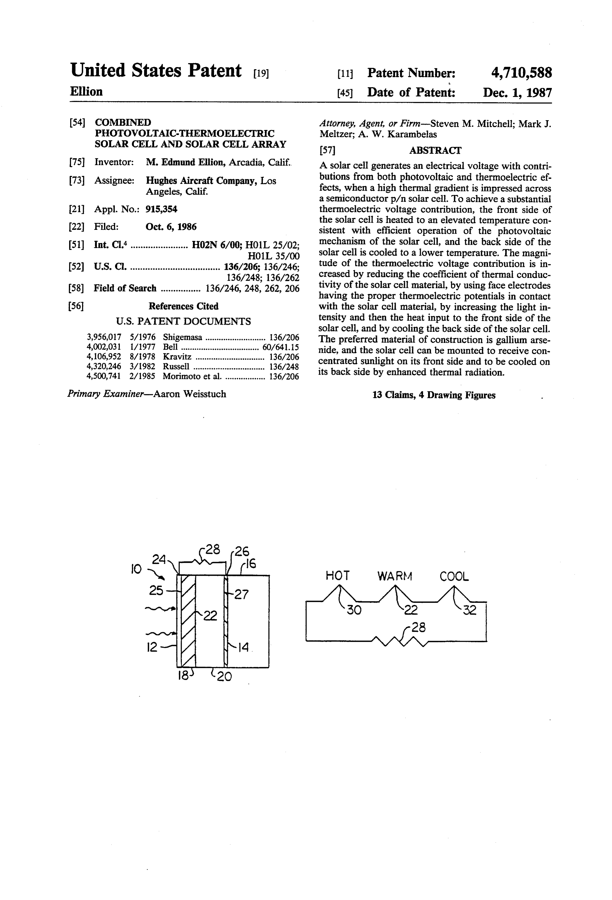
United States Patent (19) 11j Patent Number: 4,710,588 Ellion 45) Date of Patent: Dec. 1, 1987 54 COMBINED Attorney, Agent, or Firm-Steven M. Mitchell; Mark J. PHOTOVOLTAC-THERMOELECTRIC Meltzer; A. W. Karambelas
SOLAR CELL AND SOLAR CELL ARRAY
75 Inventor: M. Edmund Ellion, Arcadia, Calif. A solar cell generates an electrical voltage with contri 73) Assignee: Hughes Aircraft Company, Los butions from both photovoltaic and thermoelectric ef. Angeles, Calif. fects, when a high thermal gradient is impressed across a semiconductor pyn solar cell. To achieve a substantial 21 Appl. No.: 915,354 thermoelectric voltage contribution, the front side of 22 Filed: Oct. 6, 1986 the solar cell is heated to an elevated temperature con sistent with efficient operation of the photovoltaic 51 Int, C. ....................... HO2N 6/00; H01L 25/02; mechanism of the solar cell, and the back side of the HO1L 35/00 solar cell is cooled to a lower temperature. The magni (52) U.S. C. .................................... 136/206; 136/246; tude of the thermoelectric voltage contribution is in 136/248; 136/262 creased by reducing the coefficient of thermal conduc 58) Field of Search ................ 136/246, 248, 262, 206 tivity of the solar cell material, by using face electrodes having the proper thermoelectric potentials in contact 56 References Cited with the solar cell material, by increasing the light in
solar cell, and by cooling the back side of the solar cell.
3,956,017 5/1976 Shigemasa ........................... 136/206 The preferred material of construction is gallium arse 4,002,031 1/1977 Bell ............ ... 60/641.15 nide, and the solar cell can be mounted to receive con 4,106,952 8/1978 Kravitz ............................... 136/206 centrated sunlight on its front side and to be cooled on 4,320,246 3/1982 Russell ................................ 136/248 4,500,741 2/1985 Morimoto et al. .................. 136/206 its back side by enhanced thermal radiation. Primary Examiner-Aaron Weisstuch 13 Claims, 4 Drawing Figures
Page 2
Drawing sheet — no readable text.
Page 3
cal contact and radiation damage such as encountered
COMBINED in a space environment, it is conventional to apply a PHOTOVOLTAC-THERMOELECTRIC SOLAR transparent cover of glass over the solar cell compo CELL AND SOLAR CELL ARRAY nents.
A number of the individual solar cells are connected
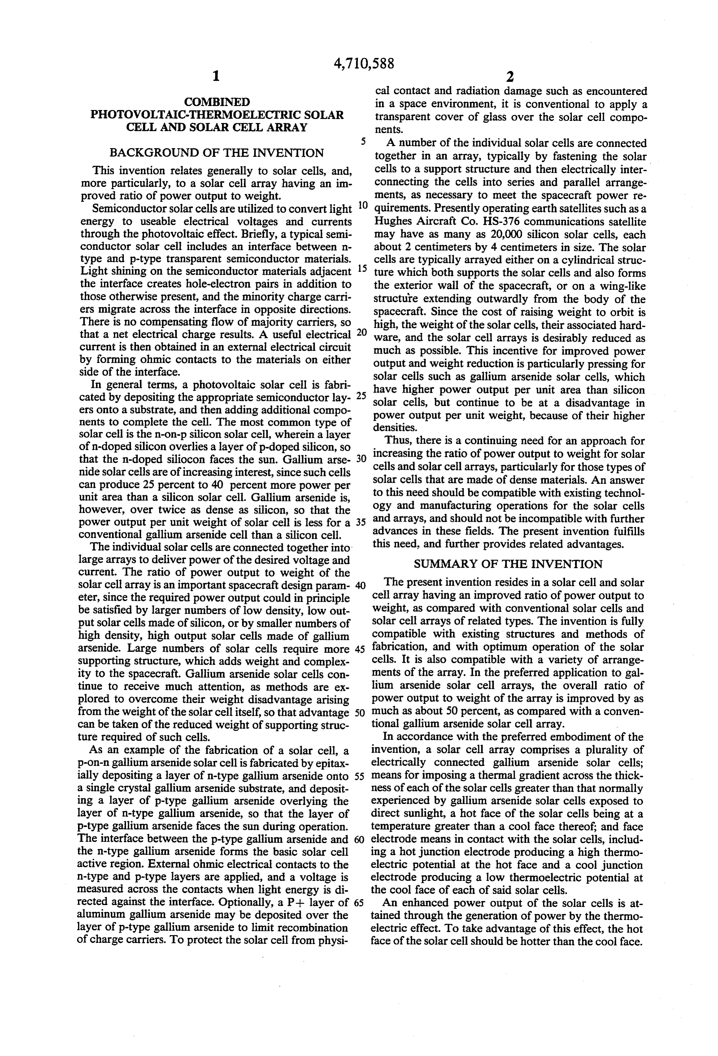
BACKGROUND OF THE INVENTION together in an array, typically by fastening the solar This invention relates generally to solar cells, and, cells to a support structure and then electrically inter more particularly, to a solar cell array having an im connecting the cells into series and parallel arrange proved ratio of power output to weight. ments, as necessary to meet the spacecraft power re Semiconductor solar cells are utilized to convert light 10 quirements. Presently operating earth satellites such as a energy to useable electrical voltages and currents Hughes Aircraft Co. HS-376 communications satellite through the photovoltaic effect. Briefly, a typical semi may have as many as 20,000 silicon solar cells, each conductor solar cell includes an interface between n about 2 centimeters by 4 centimeters in size. The solar type and p-type transparent semiconductor materials. 15 cells are typically arrayed either on a cylindrical struc Light shining on the semiconductor materials adjacent ture which both supports the solar cells and also forms the interface creates hole-electron pairs in addition to the exterior wall of the spacecraft, or on a wing-like those otherwise present, and the minority charge carri structure extending outwardly from the body of the ers migrate across the interface in opposite directions. spacecraft. Since the cost of raising weight to orbit is There is no compensating flow of majority carriers, so 20 high, the weight of the solar cells, their associated hard that a net electrical charge results. A useful electrical ware, and the solar cell arrays is desirably reduced as current is then obtained in an external electrical circuit much as possible. This incentive for improved power by forming ohmic contacts to the materials on either output and weight reduction is particularly pressing for side of the interface. solar cells such as gallium arsenide solar cells, which In general terms, a photovoltaic solar cell is fabri have higher power output per unit area than silicon cated by depositing the appropriate semiconductor lay 25 solar ers onto a substrate, and then adding additional compo powercells, but continue to be at a disadvantage in output per unit weight, because of their higher nents to complete the cell. The most common type of densities.
solar cell is the n-on-p silicon solar cell, wherein a layer Thus, there is a continuing need for an approach for of n-doped silicon overlies a layer of p-doped silicon, so increasing the ratio of power output to weight for solar that the n-doped siliocon faces the sun. Gallium arse cells and solar
cell arrays, particularly for those types of nide solar cells are of increasing interest, since such cells can produce 25 percent to 40 percent more power per solar cells that are made of dense materials. An answer unit area than a silicon solar cell. Gallium arsenide is, to this need should be compatible with existing technol however, over twice as dense as silicon, so that the ogy and manufacturing operations for the solar cells power output per unit weight of solar cell is less for a 35 and arrays, and should not be incompatible with further conventional gallium arsenide cell than a silicon cell. advances in these fields. The present invention fulfills The individual solar cells are connected together into this need, and further provides related advantages. large arrays to deliver power of the desired voltage and SUMMARY OF THE INVENTION current. The ratio of power output to weight of the solar cell array is an important spacecraft design param 40 The present invention resides in a solar cell and solar eter, since the required power output could in principle cell array having an improved ratio of power output to be satisfied by larger numbers of low density, low out weight, as compared with conventional solar cells and put solar cells made of silicon, or by smaller numbers of solar cell arrays of related types. The invention is fully high density, high output solar cells made of gallium compatible with existing structures and methods of arsenide. Large numbers of solar cells require more 45 fabrication, and with optimum operation of the solar supporting structure, which adds weight and complex cells. It is also compatible with a variety of arrange ity to the spacecraft. Gallium arsenide solar cells con ments of the array. In the preferred application to gal tinue to receive much attention, as methods are ex lium arsenide solar cell arrays, the overall ratio of plored to overcome their weight disadvantage arising power output to weight of the array is improved by as from the weight of the solar cell itself, so that advantage 50 much as about 50 percent, as compared with a conven can be taken of the reduced weight of supporting struc tional gallium arsenide solar cell array. ture required of such cells. In accordance with the preferred embodiment of the As an example of the fabrication of a solar cell, a invention, a solar cell array comprises a plurality of p-on-ngallium arsenide solar cell is fabricated by epitax electrically connected gallium arsenide solar cells; ially depositing a layer of n-type gallium arsenide onto 55 means for imposing a thermal gradient across the thick a single crystal gallium arsenide substrate, and deposit ness of each of the solar cells greater than that normally ing a layer of p-type gallium arsenide overlying the experienced by gallium arsenide solar cells exposed to layer of n-type gallium arsenide, so that the layer of direct sunlight, a hot face of the solar cells being at a p-type gallium arsenide faces the sun during operation. temperature greater than a cool face thereof; and face The interface between the p-type gallium arsenide and 60 electrode means in contact with the solar cells, includ the n-type gallium arsenide forms the basic solar cell ing a hot junction electrode producing a high thermo active region. External ohmic electrical contacts to the electric potential at the hot face and a cool junction n-type and p-type layers are applied, and a voltage is electrode producing a low thermoelectric potential at measured across the contacts when light energy is di the cool face of each of said solar cells. rected against the interface. Optionally, a P-- layer of 65 An enhanced power output of the solar cells is at aluminum gallium arsenide may be deposited over the tained through the generation of power by the thermo layer of p-type gallium arsenide to limit recombination electric effect. To take advantage of this effect, the hot of charge carriers. To protect the solar cell from physi face of the solar cell should be hotter than the cool face.
Page 4
The temperature decrease through the thickness of the the presently preferred embodiment of a gallium arse solar cell between the hot face and the cool face should nide solar cell, the preferred face electrode for both the be as great as possible, consistent with the limitation hot and cool junctions is a telluride such as lead tellu that the solar cell must be maintained within its normal ride.
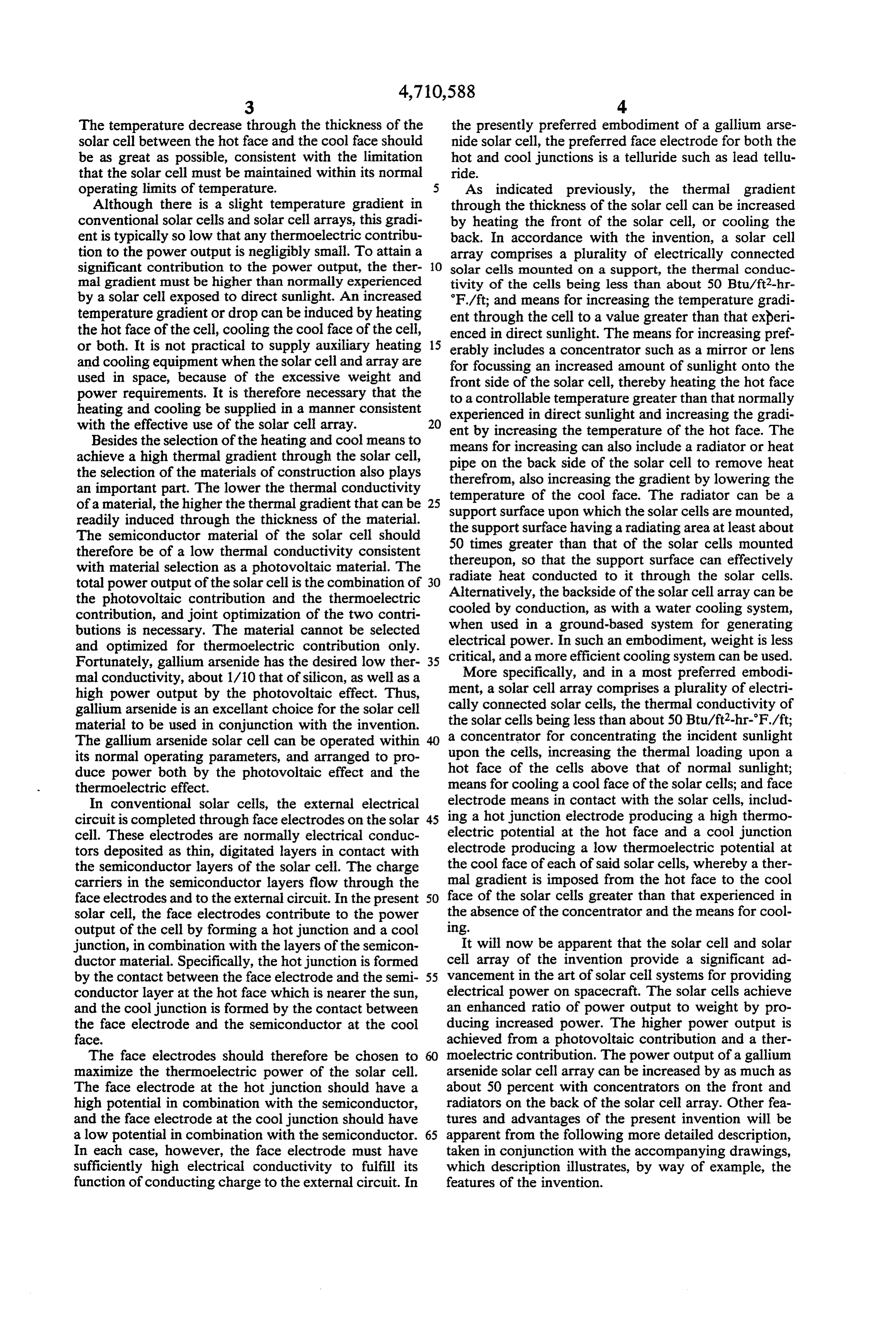
operating limits of temperature. As indicated previously, the thermal gradient Although there is a slight temperature gradient in through the thickness of the solar cell can be increased conventional solar cells and solar cell arrays, this gradi by heating the front of the solar cell, or cooling the ent is typically so low that any thermoelectric contribu back. In accordance with the invention, a solar cell tion to the power output is negligibly small. To attain a array comprises a plurality of electrically connected significant contribution to the power output, the ther O solar cells mounted on a support, the thermal conduc mal gradient must be higher than normally experienced tivity of the cells being less than about 50 Btu/ft2-hr by a solar cell exposed to direct sunlight. An increased F./ft; and means for increasing the temperature gradi temperature gradient or drop can be induced by heating ent through the cell to a value greater than that experi the hot face of the cell, cooling the cool face of the cell, enced in direct sunlight. The means for increasing pref. or both. It is not practical to supply auxiliary heating 15 erably includes a concentrator such as a mirror or lens and cooling equipment when the solar cell and array are for focussing an increased amount of sunlight onto the used in space, because of the excessive weight and front side of the solar cell, thereby heating the hot face power requirements. It is therefore necessary that the to a controllable temperature greater than that normally heating and cooling be supplied in a manner consistent experienced in direct sunlight and increasing the gradi with the effective use of the solar cell array. 20 ent by increasing the temperature of the hot face. The
Besides the selection of the heating and cool means to means for increasing can also include a radiator or heat achieve a high thermal gradient through the solar cell, the selection of the materials of construction also plays pipe on the back side of the solar cell to remove heat therefrom, also increasing the gradient by lowering the an important part. The lower the thermal conductivity temperature of the cool face. The radiator can be a of a material, the higher the thermal gradient that can be 25 support surface upon which the solar cells are mounted, readily induced through the thickness of the material. the support surface having a radiating area at least about The semiconductor material of the solar cell should therefore be of a low thermal conductivity consistent thereupon, so that the that 50 times greater than of the solar cells mounted support surface can effectively with material selection as a photovoltaic material. The radiate heat conducted to it through the solar cells. total power output of the solar cell is the combination of 30 Alternatively, the backside of the solar cell array can be the photovoltaic contribution and the thermoelectric cooled by conduction, as with a water cooling system, contribution, and joint optimization of the two contri when used in a ground-based system for generating butions is necessary. The material cannot be selected and optimized for thermoelectric contribution only. electrical power. In such an embodiment, weight is less Fortunately, gallium arsenide has the desired low ther 35 critical, and a more efficient cooling system can be used. mal conductivity, about 1/10 that of silicon, as well as a ment, More specifically, and in a most preferred embodi high power output by the photovoltaic effect. Thus, a solar cell array comprises a plurality of electri gallium arsenide is an excellant choice for the solar cell cally connected solar cells, the thermal conductivity of material to be used in conjunction with the invention. the solar cells being less than about 50 Btu/ft2-hr-F./ft; The gallium arsenide solar cell can be operated within a concentrator for concentrating the incident sunlight its normal operating parameters, and arranged to pro upon the cells, increasing the thermal loading upon a duce power both by the photovoltaic effect and the hot face of the cells above that of normal sunlight; thermoelectric effect. means for cooling a cool face of the solar cells; and face In conventional solar cells, the external electrical electrode means in contact with the solar cells, includ circuit is completed through face electrodes on the solar 45 ing a hot junction electrode producing a high thermo cell. These electrodes are normally electrical conduc electric potential at the hot face and a cool junction tors deposited as thin, digitated layers in contact with electrode producing a low thermoelectric potential at the semiconductor layers of the solar cell. The charge the cool face of each of said solar cells, whereby a ther carriers in the semiconductor layers flow through the mal gradient is imposed from the hot face to the cool face electrodes and to the external circuit. In the present 50 face of the solar cells greater than that experienced in solar cell, the face electrodes contribute to the power the absence of the concentrator and the means for cool output of the cell by forming a hot junction and a cool ing.
junction, in combination with the layers of the semicon It will now be apparent that the solar cell and solar ductor material. Specifically, the hot junction is formed cell array of the invention provide a significant ad by the contact between the face electrode and the semi 55 vancement in the art of solar cell systems for providing conductor layer at the hot face which is nearer the sun, electrical power on spacecraft. The solar cells achieve and the cool junction is formed by the contact between an enhanced ratio of power output to weight by pro the face electrode and the semiconductor at the cool ducing increased power. The higher power output is face. achieved from a photovoltaic contribution and a ther The face electrodes should therefore be chosen to moelectric contribution. The power output of a gallium maximize the thermoelectric power of the solar cell. arsenide solar cell array can be increased by as much as The face electrode at the hot junction should have a about 50 percent with concentrators on the front and high potential in combination with the semiconductor, radiators on the back of the solar cell array. Other fea and the face electrode at the cool junction should have tures and advantages of the present invention will be a low potential in combination with the semiconductor. 65 apparent from the following more detailed description, In each case, however, the face electrode must have taken in conjunction with the accompanying drawings, sufficiently high electrical conductivity to fulfill its which description illustrates, by way of example, the function of conducting charge to the external circuit. In features of the invention.
Page 5
BRIEF DESCRIPTION OF THE DRAWINGS layer 18, at the hot face 25, is a hot junction 30. The interface between the n-layer face electrode 26 and the
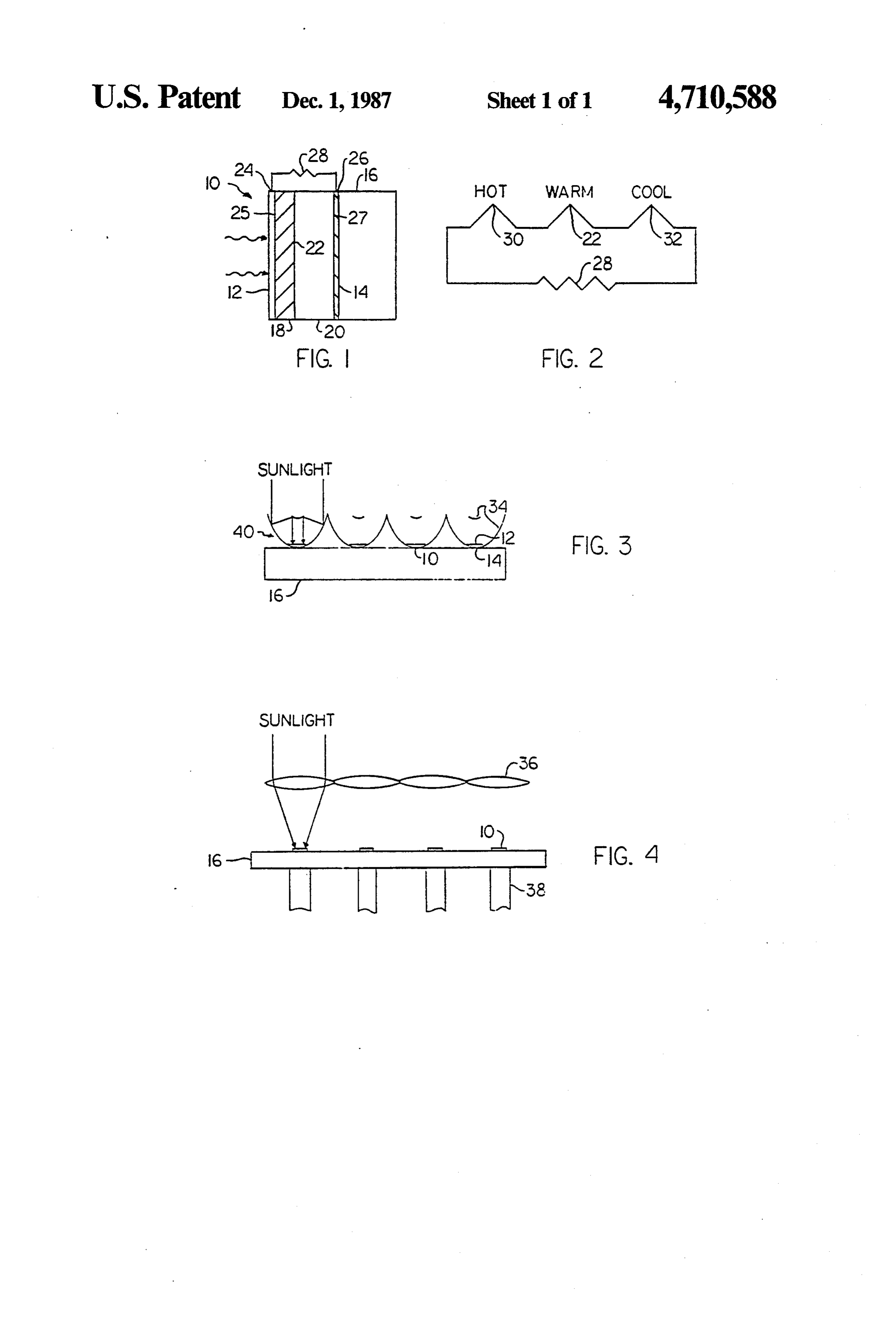
FIG. 1 is a side sectional view of a solar cell; n-doped layer 20, at the cool face 27, is a cool junction FIG. 2 is a schematic circuit diagram of the solar cell 32. The interface 22 between the p-doped layer 18 and of FIG. 1, illustrating the origin of the contributions to 5 the n-doped layer 20 is a warm junction whereat the power output; photovoltaic potential arises. FIG. 3 is a side elevational view of a preferred ar Although all solar cells have a minor thermal gradi rangement for a solar cell array; and ent through their thickness, the magnitude of the ther FIG. 4 is a side elevational view of another arrange moelectric effect has been small due to the low tempera ment for a solar cell array. O ture difference of about 0.01 F. across the normal un DETALED DESCRIPTION OF THE concentrated silicon solar cell. A typical solar cell is on PREFERRED EMBODEMENT the order of about 0.010 inches in thickness, and a low temperature difference results in a temperature gradient
The origins of the photovoltaic and thermoelectric and thermoelectric effect that are negligible. contributions to the solar cell power output are illus 15 In order to have a significant thermoelectric effect, trated in FIGS. 1 and 2. FIG. 1 depicts the elements of the magnitude of the thermal gradient through the a solar cell 10, here shown as a p-on-ngallium arsenide thickness of the solar cell 10 must be increased above solar cell. A front side 12 of the solar cell 10 faces the that produced by normal incident sunlight. This in sun, while a back side 14 rests upon a support 16. The creased gradient can be achieved by increasing the solar cell 10 includes a p-doped layer 18 overlying an temperature at the hot face 12, decreasing the tempera n-doped layer 20, so that an interface 22 is formed be ture at the cool face 14, selecting a solar cell material tween the two layers 18 and 20. Light photons of the having a low thermal conductivity, selecting materials proper energy are absorbed by the layers 18 and 20, having high thermoelectric potentials in combination at creating hole-electron pairs. Due to the internal poten the junctions, or any combination of these actions. tial energy state of the solar cell 10 in the neighborhood 25 The temperature of the hot face 12 is most conve of the interface 22, electrons accumulate in the n-doped niently increased by concentrating the available energy, regions, and holes accumulate in the p-doped regions, sunlight, upon the front side 12. Concentration of the creating a permanent electric field within the solar cell sunlight increases the temperature of the hot face 25 and 10. The voltage created in this manner is a photovoltaic the hot junction 30. The concentration of sunlight can potential, and does not depend upon the presence of a 30 be accomplished by any convenient means, such as thermal gradient within the solar cell 10. It is this photo mirrors 34 illustrated in FIG. 3, or lenses 36 illustrated electric voltage that is the source of the potential and in FIG. 4. The temperature of the hot junction 30 may current in conventional semiconductor solar cells. be increased to arbitrarily high temperatures using mir In accordance with the invention, a further contribu rors or lenses, but the desired maximum temperature is tion to the useable voltage is supplied by the thermo 35 determined by the decreasing efficiency of the photo electric effect, also sometimes called the Seebeck effect. voltaic output of the solar cell 10 with increasing tem A thermoelectric voltage is developed in a thermal perature. The desired maximum temperature is depen gradient, created by a temperature difference, because dent upon the material of the solar cell 10, but for a of the thermal diffusion of electrons and holes. In a gallium arsenide cell the preferred maximum tempera material having an internal thermal gradient and free 40 ture has been determined to be about 200 F. electrons, the charge carriers have greater thermal mo The thermal gradient can be increased by cooling the tion in regions having higher temperature. Thermal back side 14 by radiating heat to space, thence cooling diffusion of electrons builds up an excess of electrons in the cool face 27 and the cool junction 32. Typically, for the cool regions, thereby creating an electric field and a concentrator cell the cool junction 32 operates at a associated thermoelectric voltage. Charge carriers tend 45 temperature of about 150 F., with such cooling in oper to diffuse internally so as to decrease the electric field, ation. The back side 14 can be cooled by any suitable but internal resistance and the potential energy near the means, as by forming the support 16 of an efficiently interface 22 reduce the ability of the charge carriers to radiating material such as one having a high thermal flow internally. Thus, a material such as a semiconduc emissivity and a high thermal conductivity. The radiat tor having a degree of internal resistance can develop an 50 ing area of the support 16 is also made much larger than appreciable thermoelectric potential. the effective area of the solver cells 10 that produce The photovoltaic and thermoelectric effects work power because of the concentrators, so that the heat together in creating an additive electric field in the solar from the solar cell 10 can be efficiently radiated to the cell 10 of the present invention. Both phenomena result vacuum environment of space as illustrated in FIG. 3. in electrons being accumulated in the n-doped layer 20 55 In another approach, heat can be removed from the of the solar cell 10, and holes being accumulated in the cool face 14 with heat pipes 38, illustrated in FIG. 4. In p-doped layer 18. An external electric current can be yet another approach useful in ground-based solar cell produced from the permanent electrical field by attach arrays, the back side can be cooled by conduction, as ing a p-layer face electrode 24 to a hot face 25 of the with a cooling fluid such as water. This alternative is p-doped layer 18, and an in-layer face electrode 26 to a heavier but provides a higher rate of heat extraction cool face 27 of the n-doped layer 20, and then electri from the bakc side 14 to boost the temperature gradient cally connecting the electrodes 24 and 26 through an and thence the efficiency of the solar cell 10. external resistance 28. Although the hot face 25 and the It is essential that the material of the solar cell 10 be cool face 27 are illustrated in FIG. 1 to be adjacent the selected to have a relatively low coefficient of thermal front side 12 and the back side 14, respectively, the faces 65 conductivity. Even if the front side 12 of the solar cell 25 and 27 can be buried inside the solar cell 10. 10 is heated to a relatively high temperature, if the As schematically illustrated in FIG. 2, the interface coefficient of thermal conductivity is high there will not between the p-layer face electrode 24 and the p-doped be a high thermal gradient developed within the solar
Page 6
cell 10. Instead, there will be a high heat flux without that normally experienced by gallium arsenide the necessary gradient. solar cells exposed to direct sunlight, a hot face of It has been determined that the coefficient of thermal said solar cells being at a temperature greater than conductivity of the solar cell material should be less a cool face thereof; and than about 50 Btu/ft2-hr-F./ft for a solar cell of con 5 face electrode means in contact with said solar cells, ventional thickness. If materials of higher conductivity including a hot junction electrode producing a high are used, the slight increase in efficiency over a conven thermoelectric potential at said hot face and a cool tional solar cell is not sufficient to justify the change. junction electrode producing a low thermoelectric Fortunately, gallium arsenide has a coefficient of ther potential at said cool face of each of said solar cells. mal conductivity of about 30 Btu/ft2-hr-F./ft, and 10 2. The solar cell array of claim 1, wherein said said meets this requirement. The low coefficient of thermal face electrodes are lead telluride.
conductivity permits a high thermal gradient within the 3. The solar cell array of claim 1, wherein said means solar cell, if a sufficiently high temperature is applied to for imposing includes means for increasing the tempera the front side 12. ture of said hot face of said solar cells. The thermoelectric effect and its contribution to the 15 4. The solar cell array of claim 1, wherein said means total output of the solar cell 10 can be further improved for imposing includes a mirror for concentrating sun by selecting materials having desirable thermoelectric light onto said hot face of said solar cells. potentials. The material for the hot junction face elec trode 24 should have an inherently high thermoelectric for5.imposing The solar cell array of claim 1, wherein said means includes a lens for concentrating sunlight potential in combination with the layer 18 to which it is 20 onto said hot face of said solar cells. bonded. The cool junction face electrode 26 should have an inherently low thermoelectric potential in con for6.imposing The solar cell array of claim 1, wherein said means includes means for removing heat from bination with the layer 20 to which it is bonded, inas said cool face of said solar cells. much as its potential is opposite to that of the hot junc tion and the photovoltaic effect, but is much smaller in 25 for7.imposing
The solar cell array of claim 1, wherein said means magnitude. The selection of the materials used in the said cells are includes mounted, a radiating support upon which said radiating support having a face electrodes depends upon the materials of the solar radiating area at least about cell. For a gallium arsenide solar cell, the preferred active area of said solar cells.50 times greater than the material for both the p-layer face electrode 24 and the 8. The solar cell array of claim 1, wherein said means n-layer face electrode 26 is lead telluride. 30 for imposing includes a heat pipe for removing heat
For a conventional gallium arsenide solar cell operat from the cool face of said solar cells. ing at 200' F., the cell efficiency is about 15.5 percent. 9. A solar cell array, comprising: Concentrating the light of the sun on the hot face of the cell with a concentration ratio of 50 (that is, collecting a plurality of electrically connected solar cells, the sunlight from an area 50 times larger than the area of the 35 thermal conductivity of said solar cells being less solar cell, and concentrating that light onto the face of than about 50 Btu/ft2-hr-F./ft; the solar cell), the efficiency rises to about 18.6 percent. a concentrator for concentrating the incident sunlight By operating with the preferred solar cell array 40 upon said cells, increasing the thermal loading illustrated in FIG. 3 having a ratio of radiating area to upon a hot face of said cells above that of normal active solar cell area of about 50, and so that the temper 40 sunlight;
ature of the hot face is about 200 F. and the tempera means for cooling a cool face of said solar cells; and ture of the cool face is about 150 F., the efficiency is face electrode means in contact with said solar cells, raised to about 22 percent, a 40 percent increase over an including a hot junction electrode producing a high unconcentrated cell and an 18 percent increase over a thermoelectric potential at said hot face and a cool concentrated cell not having the through-thickness 45 junction electrode producing a low thermoelectric cooling that promotes a thermoelectric potential. potential at said cool face of each of said solar cells, Thus, the present invention permits the improvement whereby a thermal gradient is imposed from the in solar cell output power by judicious selection of hot face to the cool face of said solar cells greater materials of construction and array design, to obtain a than that experienced in the absence of said con significant contribution from the thermoelectric effect 50 centrator and said means for cooling. as well as the photovoltaic effect. Although a particular 10. The solar cell array of claim 9, wherein said solar embodiment of the invention has been described in cells are gallium arsenide solar cells. detail for purposes of illustration, various modifications 11. The solar cell array of claim 9, wherein said may be made without departing from the spirit and means for cooling is a support upon which said cells are scope of the invention. Accordingly, the invention is 55 mounted, the radiating area of said support being at not to be limited except as by the appended claims. least 50 times that of the power-producing area of said What is claimed is: solar cells.
1. A solar cell array, comprising: 12. The solar cell array of claim 9, wherein said a plurality of electrically connected gallium arsenide means for cooling is a heat pipe.
solar cells; 13. The solar cell array of claim 9, wherein said solar means for imposing a thermal gradient across the cells are gallium arsenide.
thickness of each of said solar cells greater than : : e :
Provenance
- Collection
- Cited prior art
- Original PDF
- patentimages.storage.googleapis.com →
- Filed
- 1986-10-06
- Pages
- 6
- Method
- pdftotext (the PDF's own text layer) + pdftoppm 300dpi page scans
- Source
- Google Patents bibliographic record
- Granted
- 1987-12-01
- Inventors
- M. Edmund Ellion; Hughes Aircraft Co
- Transcribed from
- patentimages.storage.googleapis.com →