patent · US6222116
Pre-equilibrium chemical reaction energy converter
24 April 2001
Page 1 — bibliographic record
(12) United States Patent (10) Patent No.: US 6,222,116 B1 Zupper0 et al. (45) Date of Patent: Apr. 24, 2001
(54) PRE-EQUILIBRIUM CHEMICAL REACTION OTHER PUBLICATIONS
ENERGY CONVERTER
"Electron-hole pair creation by reactions at metal Surfaces', (75) Inventors: Anthony C. Zuppero, Idaho Falls, ID downloaded from www.aps.org/meet/CENT99/BAPS/ (US); Jawahar M. Gidwani, San abs2S6980001.html American Physical Society Centennial Francisco, CA (US) Meeting Program, Atlanta, GA. 20-26 Mar. 1999. “Electron-Hole Pair Creation at Ag and Cu. Surfaces by (73) Assignee: Neokismet, L.L.C., San Francisco, CA Adsorption of Atomic Hydrogen and Deuterium”, Physical (US) Review Letters, vol. 82, No. 2. Jan. 11, 1999. Primary Examiner Mark Chapman (*) Notice: Subject to any disclaimer, the term of this (74) Attorney, Agent, or Firm-Baker & McKenzie patent is extended or adjusted under 35
U.S.C. 154(b) by 0 days. (57) ABSTRACT
The use of newly discovered chemical reaction products, (21) Appl. No.: 09/589,938 created when reactants combine to form products on the Surface of a catalyst, to generate electricity, beams of radia tion or mechanical motion. The invention also provides (22) Filed: Jun. 7, 2000 methods to convert the products into electricity or motion. The electric generator consists of a catalyst nanocluster,
Related U.S. Application Data nanolayer or quantum well placed on a Substrate consisting of a Semiconductor diode, and a Semiconductor diode on the (62) Division of application No. 09/304,979, filed on May 4, Surface of the Substrate near the catalyst. The device to 1999, now Pat. No. 6,114,620. generate mechanical motion consists of a catalyst (51) Int. Cl. ................................................... H01L 31/00 nanocluster, nanolayer or quantum well placed on a (52) U.S. Cl. .......................... 136/253; 136/254; 310/300; Substrate, and a hydraulic fluid in contact with the non 310/314; 310/322 reaction side of the Substrate, with the Surfaces of both the (58) Field of Search ..................................... 136/253,254; catalyst and Substrate mechanically formed to enhance the 310/300, 314, 322 unidirectional forces on the fluid. Both devices use a fuel oxidizer mixture brought in contact with the catalyst. The (56) References Cited apparatus converts a Substantial fraction of the reaction product energy into useful work during the brief interval
5,651,838 7/1997 Fraas et al. .......................... 136/256 5,932,885 8/1999 DeBellis et al. .................. 250/493.1 6 Claims, 2 Drawing Sheets
Page 2
Drawing sheet — no readable text.
Page 3
Drawing sheet — no readable text.
Page 4
PRE-EQUILIBRIUM CHEMICAL REACTION magnitude is less than approximately the mean free path of ENERGY CONVERTER the appropriate ballistic charge carrier originating in the catalyst. In one embodiment, the diode is located adjacent to
CROSS-REFERENCE TO RELATED the catalyst cluster, while in a further embodiment, the diode APPLICATIONS is located under the catalyst, as a Substrate.
This is a division of application Ser. No. 09/304,979, filed canThe charge carriers travel ballistically over distances that exceed the width of appropriately fabricated Semicon
May 4, 1999 now U.S. Pat. No. 6,114,620. ductor junctions, Similar to a thermionic effect. However, FIELD OF THE INVENTION unlike the thermionic effect, the charge carriers in the case of the present invention need not have energy greater than
The present invention relates to the extraction of electrical the work function of the material involved. The charge or mechanical energy or coherent radiation from chemical carrier motion is trapped as a difference in fermi level, or reactions occurring on the Surface of a catalyst before chemical potential, between either Side of the junction. The thermal equilibrium has been reached by the forms of the resulting Voltage difference is indistinguishable from that of released energy. 15 a photovoltaic collector. However, the charge carrier forces itself into the Valence or conduction band and the circuit
BACKGROUND INFORMATION provides a counterpart hole or electron.
Recent experimental observations have revealed clues to The present invention also provides devices and methods various catalytic processes occurring: 1) during the 0.01 for converting the energy generated by catalytic reactions to picoSecond time interval during which chemical reactants mechanical motion before the energy thermalizes. In an form bonds with the Surface of a catalyst, causing the exemplary embodiment, the converted motion is used to emission of charge carriers, Such as electrons and holes; 2) move a hydraulic fluid against a resisting pressure. during the picoSecond time interval during which reactants Recent advances in the art of quantum wells, atomically adsorb and lose energy in quantum Steps after becoming Smooth Superlattices and nanometer Scale fabrication permit trapped at a potential well between an adsorbate and a 25 a degree of tailoring of the physical parameters to favor a catalyst Surface, producing electronic friction, charge carrier particular reaction pathway (charge carrier, phonon, photon) currents and phonon emission; and 3) during the nanoSecond or to enhance the efficiency of the energy collector. and longer time intervals during which reaction intermedi The temperature of operation of a device in accordance ates and products radiate electromagnetic energy, either with the present invention can be as low as hundreds of while trapped on a catalyst Surface or immediately after degrees Kelvin, which is much lower than the typical escaping it. These processes entail three energy releasing operational temperatures of conventional thermophotovol processes, namely: 1) charge carrier emission (electrons and taics and thermionic systems (1500 to 2500 Kelvin). holes), 2) phonon emission and 3) photon emission. Moreover, the power per mass and power per Volume The discovery of these pre-equilibrium emissions pro ultimately achievable using pre-equilibrium emissions in vides new pathways to convert the high grade chemical accordance with the present invention exceeds that of fuel energy available during pre-equilibrium phases into useful 35 cells, conventional thermo-photovoltaics, and conventional work. The term “pre-equilibrium” refers to the period, thermionic Systems.
however brief, during which the products of reactions have Furthermore, in comparison to fuel cells which require not yet come to thermal equilibrium. These products include complex ducting, the devices of the present invention allow energy emissions, Such as charge carriers, high frequency mixing of fuel and air in the same duct, thereby simplifying phonons normally associated with the optical branch lattice 40 ducting requirements.
vibrations and with acoustic branch vibrations of similar The combination of high Volume and mass power density, wavelength and energy; and excited State chemical product Simplicity, and lower temperature operation makes the meth Species. ods and devices of the present invention competitive and Prior to the discovery of these rapid energy emission uniquely useful.
pathways, the energies resulting from a catalytic process, 45
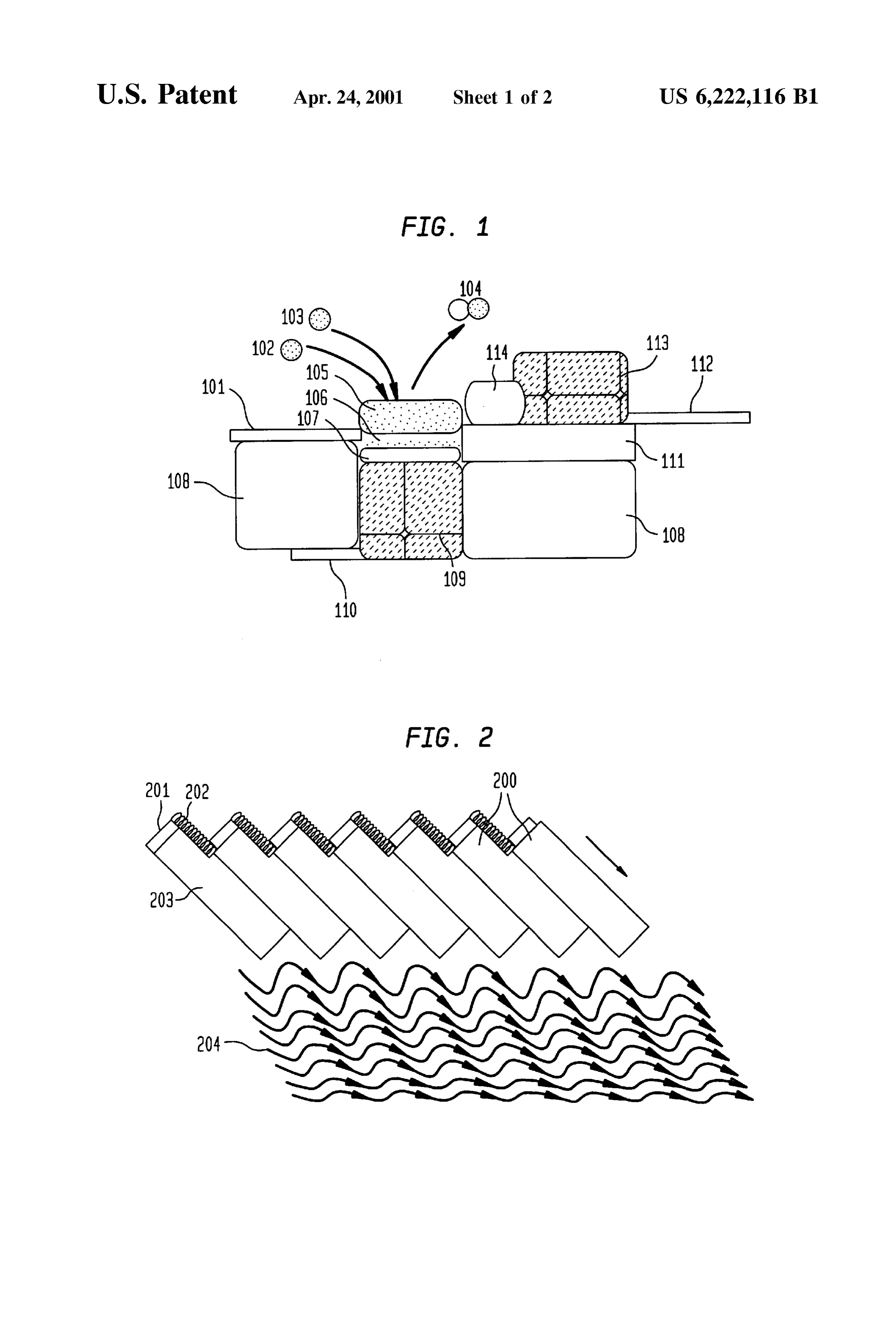
Such as the heat of adsorption and the heat of formation, BRIEF DESCRIPTION OF THE DRAWING were considered to be heat associated with an equilibrium FIG. 1. Shows a cross-section of an exemplary embodi condition. Indeed, after tens of femtoseconds, emitted ment of a device for generating electricity in accordance charge carriers have thermalized and after a few to hundreds with the present invention.
of picoSeconds, emitted phonons have thermalized. 50
FIG. 2 shows a cross-section of an exemplary embodi
SUMMARY OF THE INVENTION ment of a device for converting the energy released by a In an exemplary embodiment of the present invention, the catalytic reaction into mechanical work. emissions of charge carriers, Such as electron-hole pairs, ment of a shows
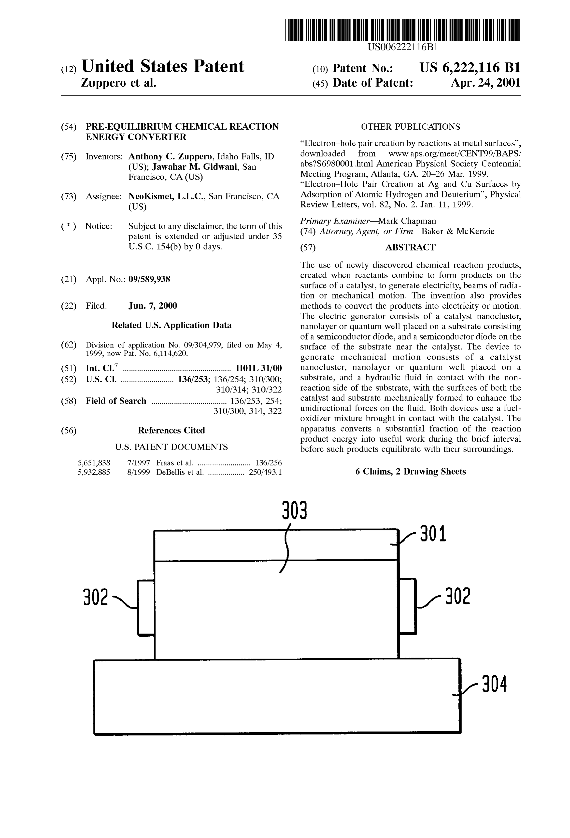
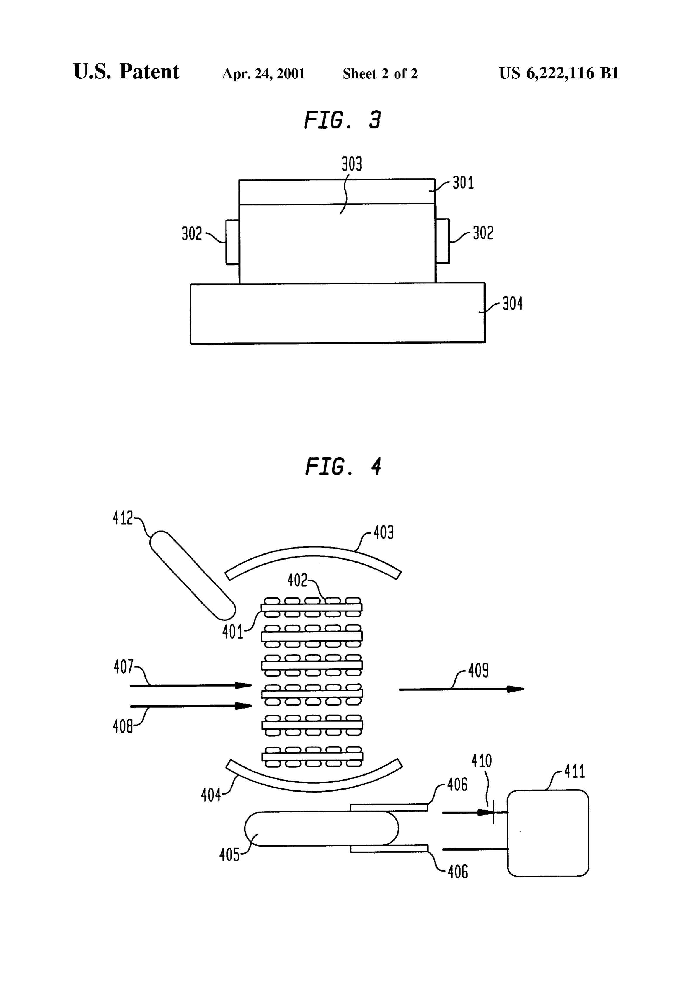
FIG. 3 a cross-section of an exemplary embodi device for generating electricity piezoelectrically.
generated by chemical activity and reactions on or within 55 catalyst Surfaces, clusters or nanoclusters, are converted into FIG. 4 shows an exemplary embodiment of an arrange electric potential. In an exemplary embodiment, Semicon ment for generating electricity or radiation beams in accor ductor diodes Such as p-n junctions and Schottky diodes dance with the present invention.
formed between the catalyst and the Semiconductors are DETAILED DESCRIPTION used to carry out the conversion. The diodes are designed to 60 collect ballistic charge carriers and can be Schottky diodes, FIG. 1 shows a cross-sectional view of an exemplary pn junction diodes or diodes formed by various combina embodiment of a device in accordance with the present tions of metal-Semiconductor-oxide Structures. The inter invention. The device of FIG. 1, includes a catalyst 105 layer oxide thickneSS is preferably less than the particular which is arranged on a top Surface of the device to come into ballistic mean free path asSociated with the energy loss of contact with oxidizer molecules 103 and fuel molecules 102. the appropriate charge carrier (e.g., hole or electron). The 65 In the exemplary embodiment of FIG. 1, the catalyst 105 can diodes are placed in contact with or near the catalyst be comprised of platinum or palladium, the oxidizer 103 can nanolayer or nanocluster within a distance whose order of be comprised of air and the fuel 102 can be comprised of
Page 5
hydrogen or a reactant hydrocarbon Such as methanol or of metal that permits matching the lattice parameters of the ethanol. Exhaust molecules 104 result from the. catalyzed catalyst to this interlayer. The catalyst 105 and interlayer 106 reaction. comprise the quantum well. The interlayer 106 must be The exemplary device of FIG. 1 comprises a pair of Sufficiently thin So as to permit non-energy changing elec Schottky diodes which act as charge carrier collectors, with tron transport into the diode. The thickness of the interlayer one diode 113 being arranged on the top Surface of the 106 should be preferably less than 20 nanometers. device, adjacent to the catalyst 105 (the “adjacent surface In an exemplary embodiment of a device in accordance diode') and the other diode 109 being arranged in the with the present invention, the substrate diode 109 com substrate 108, below the catalyst (the “substrate diode”). An prises an n-type direct band gap Semiconductor with a band insulating layer 111 is arranged between the adjacent Surface gap chosen to favor the emission of energetic electrons. diode 113 and the substrate 108, as shown. The diodes 109 In a further exemplary embodiment, the thickness or and 113 preferably comprise a bipolar Semiconductor mate cluster size (if arranged in clusters) of the catalyst layer 105 rial Such as InGaASSb with a composition chosen to opti is Sufficiently Small So as to permit the appearance of band mize the chosen operating conditions. For example, the gaps, discrete electron States and catalyst properties unlike Second harmonic of a CO Stretch vibration on a catalyst 15 the same material in bulk. In this case, the catalyst 105 can Surface at 2340 per cm energies gives a photon energy of be comprised, preferably, of gold, Silver, copper, or nickel 0.58 eV. (This matches the 0.53 eV band gap of a recently and be arranged as monolayer, 200 atom clusters. developed InCaAsSb diode described in G.W. Charache et FIG. 2 shows an exemplary embodiment of a device in al., “InGaAsSb thermophotovoltaic diode: Physics accordance with the present invention in which the emis evaluation,” Journal of Applied Physics, Vol. 85, No. 4, Feb. Sions of phonons generated by adsorbing and bonding 1999). The diodes 109 and 113 preferably have relatively reactions on or within catalyst Surfaces, clusters or nano low barrier heights, such as 0.05 to 0.4 volts. Structures are converted into hydraulic fluid pressure. The Substrate diode 109 should be forward biased Suffi In accordance with the present invention, pressures gen ciently (e.g., up to 3 volts) to raise its conduction and erated by phonons directed into a catalyst body on a first Side valence bands above the fermi level of the catalyst 105 so as of the catalyst body form a phonon wave which can be to match the energy levels of the adsorbed reactants on the 25 guided by the geometry of the catalyst (or Substrate upon catalyst Surface, Such as oxygen or hydrocarbon free radi which the catalyst may be situated) So that the phonons cals. This induces resonant tunneling of energy into the travel to the other Side of the Substrate and impart a preSSure substrate diode 109 by photons. The dimension of the oxide onto a fluid. The thickness of this travel should be less than barrier or the depletion region should be kept to less than the the mean distance over which the direction of the phonon ballistic transport dimension, which is on the order of 10 remains Substantially unperturbed. The phonons arrive at an nanometerS. angle (a "grazing” angle) Such that the directional and A metal such as Mg, Sb, Al, Ag, Sn Cu or Ni may be used asymmetric pressure of the arriving phonons appears as to form an interlayer 106 between the catalyst 105 and the wave motion on the other side of the catalyst body which semiconductor of the substrate diode 109. The interlayer 106 pushes against a fluid Such as a liquid metal or Sacrificial Serves to provide a lattice parameter match between the 35 interface, causing it to move in a direction parallel to the catalyst material and the Substrate, which in turn provides a bottom Surface. An apparent negative coefficient of friction Smooth and planar interface Surface with which to construct between the wall and the fluid is exhibited due to the wave a quantum well Structure consisting of the catalyst, the motion or directed impulses along the Surface of the bottom Vacuum above and the interlayer below. A quantum well of the device.
Structure with Smooth interfaces alters the density of elec The exemplary device comprises a substrate 202 with top tron States in the directions toward the Substrate and toward 40 and bottom Surfaces having a Saw-tooth pattern, as shown in the vacuum, So as to enhance the number of electrons with the cross-sectional view of FIG. 2. The bottom Surface is in the desired energy. The thickness of the catalyst and the contact with a hydraulic fluid 204. As shown in FIG. 2, the interlayer should be Small enough to permit ballistic trans Substrate can be thought of as comprising a plurality of port of charge carriers. This dimension is typically less than Sub-structures 200 having rectangular cross-sections and 20 nanometers. Quantum well Structures with thickneSS leSS 45 arranged adjacent to each other at an angle with respect to than 0.5 nanometer are possible in the present State of the art. the hydraulic fluid 204.
The quantum well Structure may be constructed as an island, At the top surface of the substrate, each sub-structure 200 like a pancake on a Surface (also referred to as a "quantum includes a layer 201 comprising a catalyst. On an exposed dot”). Side Surface between adjacent Sub-structures, each Sub The device of FIG. 1 may also include a non-conducting 50 structure 200 includes a layer 202 of material which is inert layer 107 arranged between the substrate diode 109 and the with respect to the catalyst and the reactants. The body of catalyst 105. The layer 107, which can be comprised of an each sub-structure is comprised of a substrate 203, which oxide, permits forward-biasing of the diode 109 without a also acts as a phonon waveguide. Platinum can be used for significant increase in the forward current. The layer 107 the catalyst layer 201 and for the Substrate 203 with air as the provides a barrier against Such forward current. An optional 55 oxidizer, ethanol or methanol as the hydrocarbon reactant oxide 114 barrier may also be arranged on the Surface of the fuel and water or mercury as the hydraulic fluid 204. The device between the catalyst 105 and the surface diode 113. hydraulic fluid can also serve as a coolant for the device, Electrical contacts 101, 110 and 112 are arranged as thereby permitting high power density operation. shown in FIG. 1. Contacts 101 and 110 serve as electrical The catalyst 201 and substrate 203 may be comprised of output leads for the substrate diode. Contacts 101 and 112 60 the same material, e.g., platinum. Other Substrate materials are the electrical output leads for the Surface diode. may be based on Structural considerations, manufacturabil In the device of FIG. 1, the catalyst layer 105 may ity and/or impedance matching So as to maximize the comprise a quantum well Structure (including quantum dots) propagation of the phonon motion into the hydraulic fluid. having a thickness typically less than 20 nm and being The thickness of the platinum catalyst layer 201 and Sufficiently Small So as to alter the density of electron States Substrate 203 should be less than the energy-changing mean in the catalyst to favor the production of Substantially 65 free path of optical branch phonons or high frequency monoenergetic holes or electrons. The Substrate diode 109 acoustic branch phonons, which is at least of order 10 and the catalyst 105 may be separated by an interlayer 106 nanometers and can be as large as one micron.
Page 6
S 6
Nanofabrication methods can be used to form the saw tude atomic motions at the focus. The atomic motions tooth patterns on the surfaces of the Substrate 202, with the induced by this focusing cause the piezoelectric material to dimension of a unit of Such pattern being as large as 1 become nonlinear, causing non-linear responses Such as the micron. generation of electricity in the material at the focus. This in By depositing the inert layerS 202 as shown, e.g., on the turn results in the piezo-material becoming a rectifier of the right-facing facets of the Saw-tooth pattern of the top phonon-induced high frequency current.
Surface, a preferential direction is thereby established for Acoustic, ultraSonic or gigahertz acoustic Rayleigh waves reactions and thus for phonon propagation, as indicated by can be used on the catalyst Side of the exemplary device of the arrow in FIG. 2. FIG. 3 to stimulate the reaction rate and synchronize the Acoustic, ultraSonic or gigahertz acoustic Rayleigh waves emission of phonons, to enhance the magnitude of the on the catalyst Side can be used to Stimulate the reaction rate phonon emission and to cause coherent emission, greatly and Synchronize the emission of phonons. The waves enhancing bothmaterial the peak and average power delivered to the increase the magnitude of the phonon emission and cause piezoelectric 303. Acoustic Rayleigh waves accel coherent emission, greatly enhancing both the peak and erate oxidation reactions on platinum catalyst Surfaces. average power. 15
Surface acoustic waves can be generated on the Surface of
In a further embodiment, a thin layer or layers of material maycatalyst the have 301 using a generator (not shown). Such waves acoustic, ultrasonic or gigahertz frequencies. The are arranged between the Substrate and the fluid. These Rayleigh waves induce reactions So as to Synchronize the layers are comprised of materials having acoustic imped reactions, which in turn Synchronizes the emission of ances between that of the substrate 202 and the hydraulic phonons. The result is a pulsing bunching of the reactions, fluid 204, So as to maximize the transmission of momentum which enhances the power delivered to the piezoelectric into the hydraulic fluid and minimize reflections back into material 303.
the Substrate 204. The material should be selected So that the bulk modulus and phonon propagation properties of the preferably The frequency of operation of the device of FIG. 3 is material cause the phonons emerging from the Substrate to of the alternating in the GHz range and lower so that rectification be transmittied substantially into the fluid with minimal 25 material 303 can be currents produced by the piezoelectric achieved with conventional means, Such reflection and energy loSS. as with Semiconductor diodes.
In a further embodiment of a device in accordance with the present invention, the emissions of phonons generated invention, In a further exemplary embodiment of the present by catalytic reactions are converted into electrical current by tons emittedelectromagnetic radiation, Such as infrared pho piezo-electric effects within materials as the phonons impact tionally excited radicals andproducts by excited State final
Such as highly vibra product molecules, is the materials. An exemplary embodiment of Such a device is converted into electricity photovoltaically. Stimulated emis shown in FIG. 3.
Sion of radiation is used to extract the energy
The exemplary device of FIG.3 comprises a catalyst layer excited State products, Such as highly vibrationally excited from the 301 arranged on a piezo-electric element 303, which is in radical and reaction product molecules both on the catalyst turn arranged on a Supporting Substrate 304. The catalyst Surface and desorbing from it. The extracted energy appears layer 301 can be implemented as a nanocluster, nanolayer or 35 in the form of a coherent beam or a Super-radiant beam of quantum well. Electrical leads 302 are provided at opposite infra-red or optical energy. The frequencies of the radiation ends of the piezoelectric element 303 across which a poten correspond to fundamental (vibration quantum number tial is developed, in accordance with the present invention. change of 1) or overtones (vibration quantum number In the exemplary embodiment of FIG. 3, the catalyst layer change 2 or greater) of the normal mode vibration frequen 301 comprises platinum, with air as the oxidizer and ethanol 40 cies of the reactants. Several different frequencies may be or methanol as the hydrocarbon reactant fuel. The piezo extracted simultaneously in this invention. While the result electric element 303 can comprise any piezomaterial, ing coherent beam is useful in its own right, this high including. Semiconductors that are not normally intensity beam can also be photovoltaically converted into piezoelectric, Such as InGaAsSb. The lattice mismatch electricity. In accordance with the present invention, Such between the Semiconductor and the platinum produces a 45 emissions are created by reactions on catalyst Surfaces, and Strain, commonly called a deformation potential which are accelerated by the use of optical cavities. FIG. 4 shows induces piezoelectric properties in Semiconductors, or fer an exemplary embodiment of an electric generator for roelectric or piezoelectric materials with a high nonlinearity performing Such a conversion.
such as (Ba, Sr)TiO3 thin films, AlxGa1-xAS/GaAs and strained layer InCaAS/GaAs (111) B quantum well p-i-n 50 401Theupon device of FIG. 4 comprises one or more substrates which a catalyst 402 is arranged in a plurality of
StructureS.
islands, nanoclusters, quantum well clusters or quantum
Where the piezoelectric element 303 is comprised of a dots. The catalyst clusters are Sufficiently spaced apart (e.g., Semiconductor, the Semiconductor becomes a diode element tens of nanometers or more) and the Substrate is made that converts photons into electricity, collects electrons as Sufficiently thin (e.g., less than a centimeter total optical electricity, and converts phonons into electricity. thickness), So that IR absorbtion is mitigated at the frequen In the exemplary embodiment of FIG. 3, as the reactants 55 cies of Specie emission. The assembly of catalyst clusters on interact with the catalytic layer 301, phonons generated by the Substrates 401 is substantially transparent to the reaction the reactions are conducted into the piezoelectric material radiations. The catalyst 402 is preferably platinum or pal 303. AS a result, a potential is induced in the piezoelectric ladium. The device preferably comprises a plurality of material 303 at the electrical contacts 302. Substrates 401 Stacked So as to permit a volume of reactions. The geometry of the substrate 303 is preferably such as to 60 The catalyst-substrate stack 401/402 is enclosed in an focus phonons So as to enhance the nonlinearity of the optical cavity having a highly reflective element 403 and a piezoelectric element 303. This results in self-rectification of less reflective element 404 arranged as shown in FIG. 4. The the high frequency phonons. In an exemplary embodiment, optical cavity and the catalyst-substrate stack 401/402 are the piezoelectric element 303 is preferably curved and preferably resonant to the reaction radiations or their over shaped like a lens or concentrating reflector So as to focus 65 tones. The optical cavity can be used to Stimulate overtone the phonons generated by the catalyst on to the piezoelectric radiation, i.e., multipole radiation where the change in material. The focusing of the phonons causes large ampli quantum number is 2 or more, to increase the energy of the
Page 7
radiation. The optical cavity preferably has multiple rotate. These features permit a near monochromatic over frequencies, as in a Fabrey-Perot cavity, that are tuned to tone light amplification by Stimulated emission of radiation. overtones of the Specie frequencies. The electromagnetic energy radiated by the Stimulation of A fuel 407, Such as hydrogen, ethanol or methanol and an species, as in the embodiment of FIG. 4, can be formed into oxidizer 408, such as air, are introduced into the optical high brightness, quasi-monochromatic, poly-chromatic cavity where they interact with the catalyst-Substrate Stack radiations or coherent beams.
401/.402. Lean mixtures of fuel can be used so as to In each of the above described embodiments which minimize resonant transfer, exchange or decay of excited include photovoltaic Semiconductors, the catalyst is prefer State vibrational energy to other Specie of the same chemical ably operated at a high Surface power density, e.g., in exceSS makeup in the exhaust Stream, during the time these Species of 10 watts per Square centimeter or with a peak Surface are in the optical cavity and the photovoltaic converter 405 power density of at least one watt per Square centimeter, to collects the radiation and converts it into electricity. enhance the efficiency of the photovoltaic Semiconductors. A Stimulated emission initiator and Synchronizer device What is claimed is:
412 is used to initiate and Synchronize the emissions in the 1. A device for generating electricity comprising: optical cavity. The device 412 can be a commonly available 15 a catalyst; and
Stimulated emission oscillator and can be coupled to the a Substrate, wherein the catalyst is arranged on a Surface device of the present invention in known ways. The optical of the Substrate and the Substrate includes a piezoelec cavity can be designed in a known way to create Stimulated tric element, emission of radiation. A photovoltaic cell is typically not wherein phonons generated upon interaction of the very efficient in converting long wavelength IR photons catalyst with reactants travel through the piezoelec (1000 to 5000 per centimeter) characteristic of the catalytic tric element which develops an electrical potential as reactions. The high peak power output of the device 412 a result.
remedies this situation and makes the IR photovoltaic cell more efficient. 2. The device of claim 1, wherein the catalyst includes at A photovoltaic converter 405 is placed outside the volume least one of a nanocluster, nanolayer and a quantum well. 3. The device of claim 1, wherein the piezoelectric of the catalyst-substrate stack 401/402 anywhere visible to 25 element the emitted radiation. Such a placement allows cooling the propertiesincludescaused a Semiconductor having piezoelectric by a lattice mismatch between the Semi photovoltaic collector 405 using known methods. The elec conductor and the catalyst.
trical output leads 406 of the photovoltaic collector 405 can 4. The device of claim 1, wherein the Substrate focuses be coupled to an electrical energy Storage device 411 via a phonons So as to enhance a non-linear responses. diode 410. The output of the photovoltaic converter 405 is in pulses with the pulse rate typically being greater than one one5. The
device of claim 1, wherein a wave including at least an acoustic, ultraSonic and a gigahertz acoustic megahertz. The electrical energy Storage device 411 may Rayleigh wave is applied to the catalyst to Stimulate a comprise, for example, a capacitor, Super-capacitor or bat reaction rate and Synchronize the phonon emission, thereby tery. Given the high frequency of the pulsed output, a enhancing a magnitude capacitor used as the Storage device 411 can be quite 35 coherent emission. of the phonon emission and causing compact. The capacitor need only be large enough to collect 6. The device of claim 1 comprising: the energy of a Single pulse. The energy Stored in the capacitor can thus be millions of times less than the energy electrical contacts, the electrical contacts being arranged delivered by the converter 405 in one second. on the piezoelectric element, wherein the electrical The chemical reactants on the catalyst Surface permit 40 potential appears at the electrical contacts, and overtone transitions because they are part of a “ladder” of an electrical Storage device, the electrical Storage device transitions and Strongly polarized on the catalyst Surface, being coupled to the electrical contacts, wherein the which permits all the transitions to have non-Zero dipole electrical Storage device includes at least one of a radiation transition matrix elements. Also, the reactants have capacitor, a Super-capacitor and a battery. no rotational Smearing associated with free molecules in a gas because they are attached to the Surface and can not k k k k k
Provenance
- Collection
- Cited prior art
- Original PDF
- patentimages.storage.googleapis.com →
- Filed
- 2000-06-07
- Pages
- 7
- Method
- pdftotext (the PDF's own text layer) + pdftoppm 300dpi page scans
- Source
- Google Patents bibliographic record
- Granted
- 2001-04-24
- Inventors
- Anthony C. Zuppero; Jawahar M. Gidwani; Neokismet LLC
- Transcribed from
- patentimages.storage.googleapis.com →