patent · US4849799
Resonant tunneling transistor
18 July 1989
Page 1 — bibliographic record
United States Patent (19) (11) Patent Number: 4,849,799 Capasso et al. 45) Date of Patent: Jul.18, 1989 54 RESONANTTUNNELING TRANSISTOR FOREIGN PATENT DOCUMENTS 75 Inventors: Federico Capasso, Westfield, N.J.; 0068.064 1/1983 European Pat. Off. .......... 357/45 L Harry T. French, New York, N.Y.; 0159273 10/1985 European Pat. Off........... 357/45 L Arthur C. Gossard, Warren; Albert L. 58-142574 8/1983 Japan ................................. 357/45 L Hutchinson, Piscataway, both of 59-67676 4/1984 Japan................................. 357/45 L N.J.; Richard A. Kiehl, New York,
N.Y.; Sustana Sen, Scotch Plains, OTHER PUBLICATIONS
N.J. Dubon et al. "Double Heterojunction . . . Circuits', (73) Assignee: American Telephone and Telegraph IEDM Wash. D.C. 1983, pp. 689-693. Company AT&T Bell Laboratories, Yokoyama et al. "A New Functional ... (RHET)”Jap. Murray Hill, N.J. J. of Appl. Phys, vol. 24, No. 11, Nov. 85, pp. 853-854. Miller et al. "Parabolic System” Physical Review B vol.
21 Appl. No.: 897,378 29 No. 6. Mar. 15, 1984 pp. 3740-3743. 22 Filed: Aug. 18, 1986 Woodland Practical Electronics London McGraw-Hill. Primary Examiner-Andrew J. James
Related U.S. Application Data Assistant Examiner-Jerome Jackson, Jr.
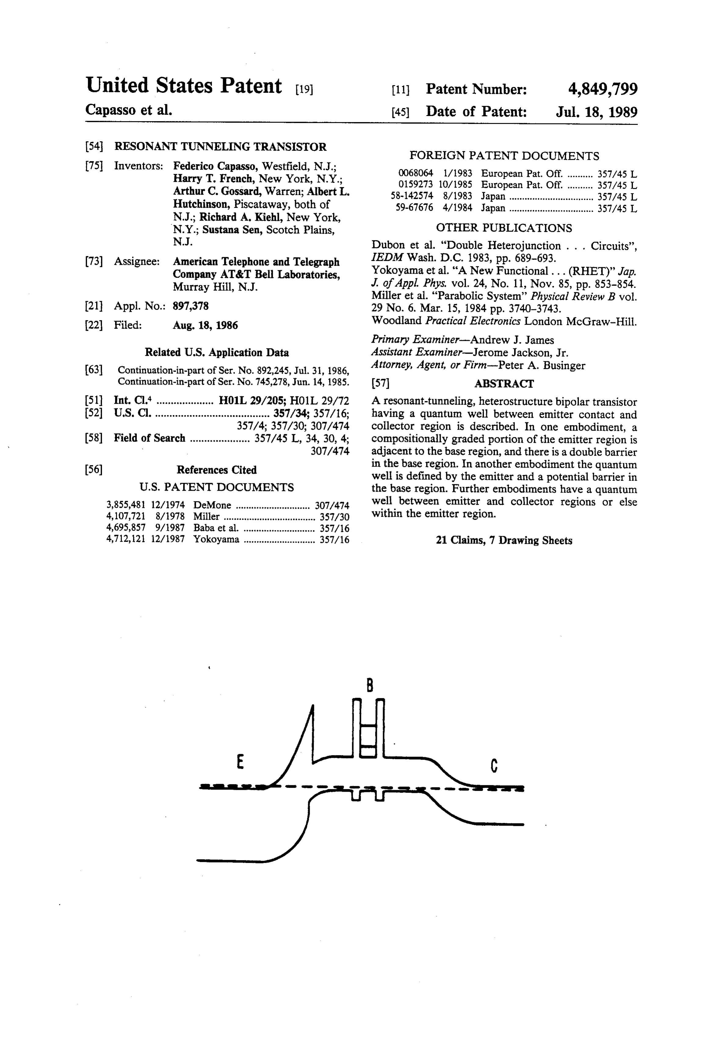
(63) Continuation-in-part of Ser. No. 892,245, Jul. 31, 1986, Attorney, Agent, or Firm-Peter A. Businger Continuation-in-part of Ser. No. 745,278, Jun. 14, 1985. (57) ABSTRACT 51 Int. Cl." .................... H01L 29/205; HO1L 29/72 A resonant-tunneling, heterostructure bipolar transistor (52) U.S.C. ........................................ 357/34; 357/16; having a quantum well between emitter contact and 357/4; 357/30, 307/474 collector region is described. In one embodiment, a (58) Field of Search ..................... 357/45 L, 34, 30, 4; compositionally graded portion of the emitter region is 307/474 adjacent to the base region, and there is a double barrier 56) References Cited in the base region. In another embodiment the quantum well is defined by the emitter and a potential barrier in
3,855,481 12/1974 DeMone ............................. 307/474 well between emitter and collector regions or else 4,107,721 8/1978 Miller ..................................., 357/30 within the emitter region.
4,695,857 9/1987 Baba et al. ............................ 357/16 4,712,121 12/1987 Yokoyama ............................ 357/16 21 Claims, 7 Drawing Sheets
Page 2
Drawing sheet — no readable text.
Page 3
Drawing sheet — no readable text.
Page 4
Drawing sheet — no readable text.
Page 5
Drawing sheet — no readable text.
Page 6
Drawing sheet — no readable text.
Page 7
Drawing sheet — no readable text.
Page 8
Drawing sheet — no readable text.
Page 9
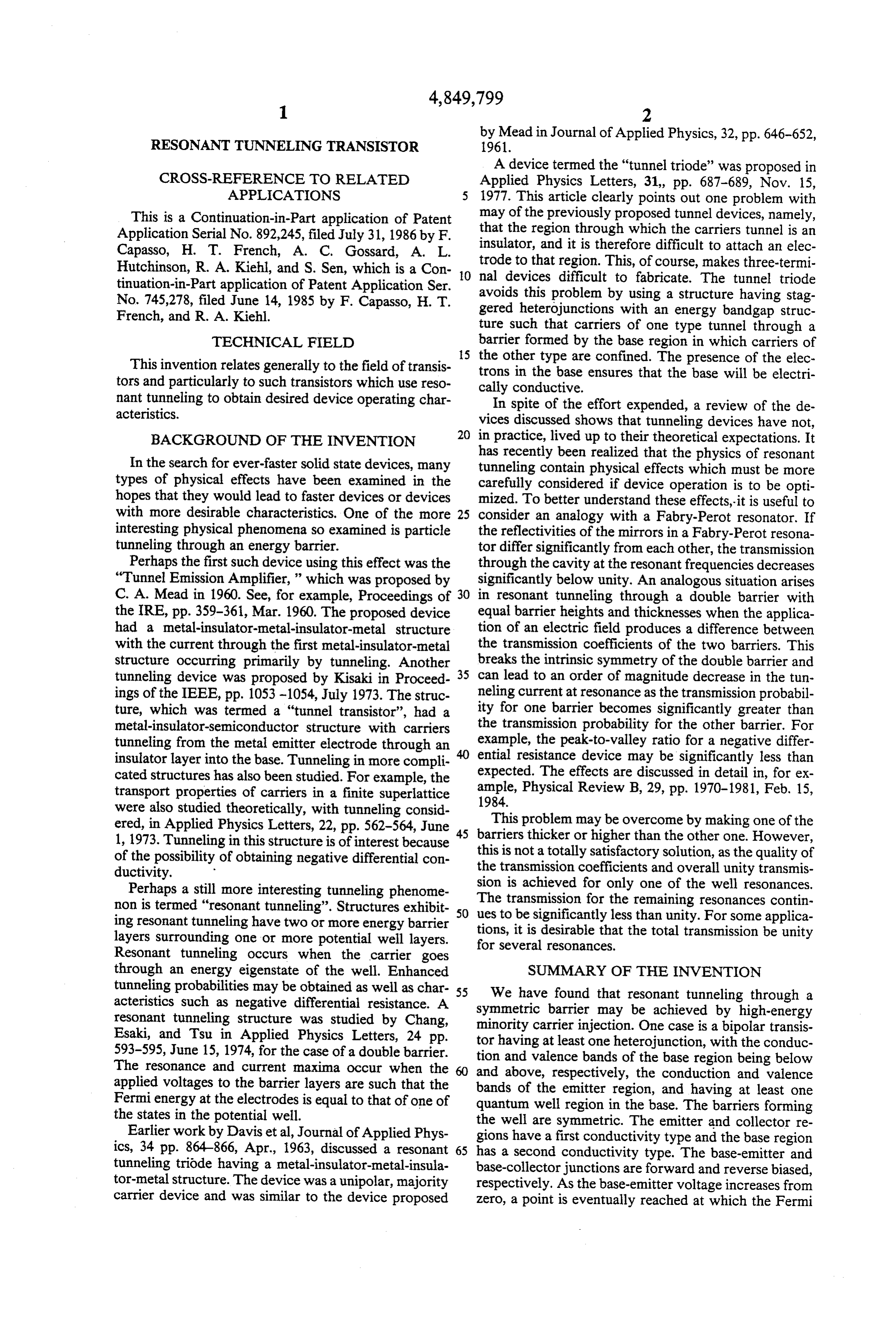
by Mead in Journal of Applied Physics, 32, pp. 646-652,
RESONANT TUNNELING TRANSISTOR 1961.
A device termed the "tunnel triode' was proposed in
CROSS-REFERENCE TO RELATED Applied Physics Letters, 31, pp. 687-689, Nov. 15, APPLICATIONS 1977. This article clearly points out one problem with This is a Continuation-in-Part application of Patent may of the previously proposed tunnel devices, namely, that the region through which the carriers tunnel is an
Application Serial No. 892,245, filed July 31, 1986 by F. insulator, and it is therefore difficult to attach an elec Capasso, H. T. French, A. C. Gossard, A. L. trode to that region. This, of course, makes three-termi Hutchinson, R. A. Kiehl, and S. Sen, which is a Con nal devices difficult to fabricate. The tunnel triode tinuation-in-Part application of Patent Application Ser. 10 avoids this problem by using a structure having stag No. 745,278, filed June 14, 1985 by F. Capasso, H. T. gered heterojunctions with an energy bandgap struc French, and R. A. Kiehl. ture such that carriers of one type tunnel through a TECHNICAL FIELD barrier formed by the base region in which carriers of 15 the other type are confined. The presence of the elec
This invention relates generally to the field of transis trons in the base ensures that the base will be electri tors and particularly to such transistors which use reso cally conductive.
nant tunneling to obtain desired device operating char In spite of the effort expended, a review of the de acteristics.
vices discussed shows that tunneling devices have not, 20 in practice, lived up to their theoretical expectations. It
BACKGROUND OF THE INVENTION
has recently been realized that the physics of resonant
In the search for ever-faster solid state devices, many tunneling contain physical effects which must be more types of physical effects have been examined in the carefully considered if device operation is to be opti hopes that they would lead to faster devices or devices mized. To better understand these effects, it is useful to with more desirable characteristics. One of the more 25 consider an analogy with a Fabry-Perot resonator. If interesting physical phenomena so examined is particle the reflectivities of the mirrors in a Fabry-Perot resona tunneling through an energy barrier. tor differ significantly from each other, the transmission Perhaps the first such device using this effect was the through the cavity at the resonant frequencies decreases "Tunnel Emission Amplifier," which was proposed by significantly below unity. An analogous situation arises C. A. Mead in 1960. See, for example, Proceedings of 30 in resonant tunneling through a double barrier with the IRE, pp. 359-361, Mar. 1960. The proposed device equal barrier heights and thicknesses when the applica had a metal-insulator-metal-insulator-metal structure tion of an electric field produces a difference between with the current through the first metal-insulator-metal the transmission coefficients of the two barriers. This structure occurring primarily by tunneling. Another breaks the intrinsic symmetry of the double barrier and tunneling device was proposed by Kisaki in Proceed 35 can lead to an order of magnitude decrease in the tun ings of the IEEE, pp. 1053-1054, July 1973. The struc neling current at resonance as the transmission probabil ture, which was termed a "tunnel transistor', had a ity for one barrier becomes significantly greater than metal-insulator-semiconductor structure with carriers the transmission probability for the other barrier. For tunneling from the metal emitter electrode through an example, the peak-to-valley ratio for a negative differ insulator layer into the base. Tunneling in more compli ential resistance device may be significantly less than cated structures has also been studied. For example, the expected. The effects are discussed in detail in, for ex transport properties of carriers in a finite superlattice ample, Physical Review B, 29, pp. 1970-1981, Feb. 15, were also studied theoretically, with tunneling consid 1984.
This problem may be overcome by making one of the ered, in Applied Physics Letters, 22, pp. 562-564, June 45 barriers 1, 1973. Tunneling in this structure is of interest because this is notthicker
or higher than the other one. However, totally satisfactory solution, as the quality of of the possibility of obtaining negative differential con ductivity. the transmission coefficients and overall unity transmis Perhaps a still more interesting tunneling phenome sion is achieved for only one of the well resonances. non is termed "resonant tunneling'. Structures exhibit 50 The transmission for the remaining resonances contin ing resonant tunneling have two or more energy barrier tions, itbeissignificantly ues to less than unity. For some applica desirable that the total transmission be unity layers surrounding one or more potential well layers. for several resonances.
Resonant tunneling occurs when the carrier goes through an energy eigenstate of the well. Enhanced SUMMARY OF THE INVENTION tunneling probabilities may be obtained as well as char 55 We have found that resonant tunneling through a acteristics such as negative differential resistance. A symmetric barrier may be achieved by high-energy resonant tunneling structure was studied by Chang, minority carrier injection. One case is a bipolar transis Esaki, and Tsu in Applied Physics Letters, 24 pp.
593-595, June 15, 1974, for the case of a double barrier. tor having at least one heterojunction, with the conduc The resonance and current maxima occur when the 60 and and tion valence bands of the base region being below applied voltages to the barrier layers are such that the bands of therespectively, above, the conduction and valence emitter region, and having at least one
Fermi energy at the electrodes is equal to that of one of quantum well region in the base. The barriers forming the states in the potential well. the well are symmetric. The emitter and collector re Earlier work by Davis et al, Journal of Applied Phys gions have a first conductivity type and the base region ics, 34 pp. 864-866, Apr., 1963, discussed a resonant 65 has a second conductivity type. The base-emitter and tunneling triode having a metal-insulator-metal-insula base-collector junctions are forward and reverse biased, tor-metal structure. The device was a unipolar, majority respectively. As the base-emitter voltage increases from carrier device and was similar to the device proposed zero, a point is eventually reached at which the Fermi
Page 10
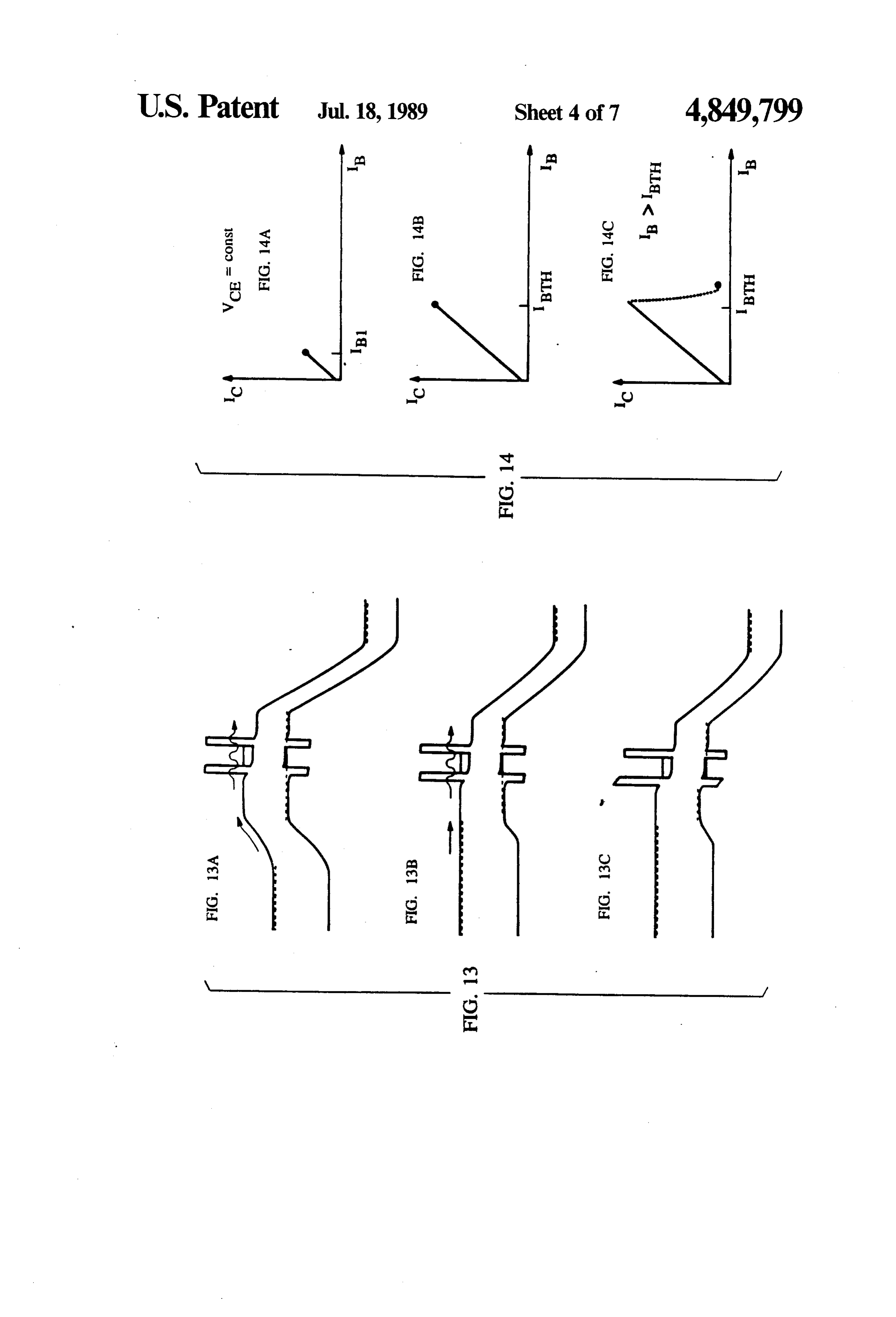
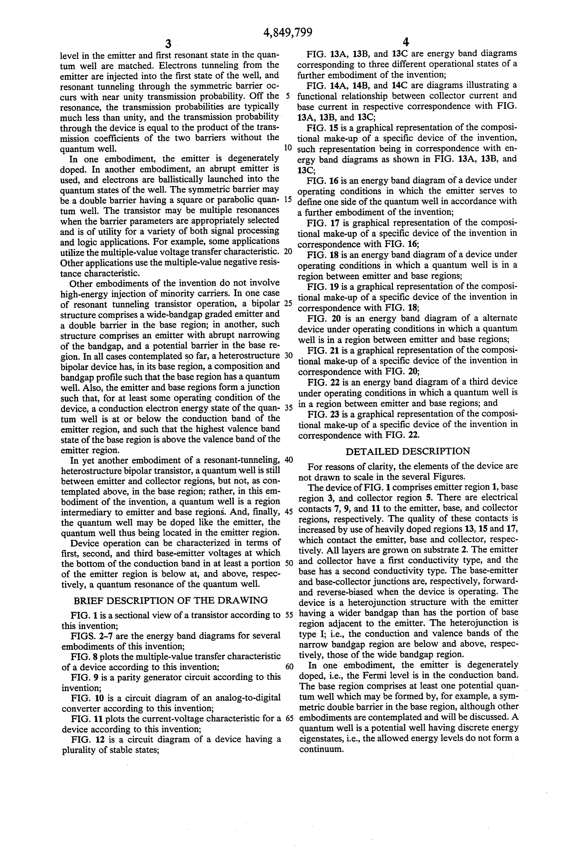
level in the emitter and first resonant state in the quan FIG. 13A, 13B, and 13C are energy band diagrams tum well are matched. Electrons tunneling from the corresponding to three different operational states of a emitter are injected into the first state of the well, and further embodiment of the invention; resonant tunneling through the symmetric barrier oc FIG. 14A, 14B, and 14C are diagrams illustrating a curs with near unity transmission probability. Off the functional relationship between collector current and resonance, the transmission probabilities are typically base current in respective correspondence with FIG. much less than unity, and the transmission probability 13A, 13B, and 13C;
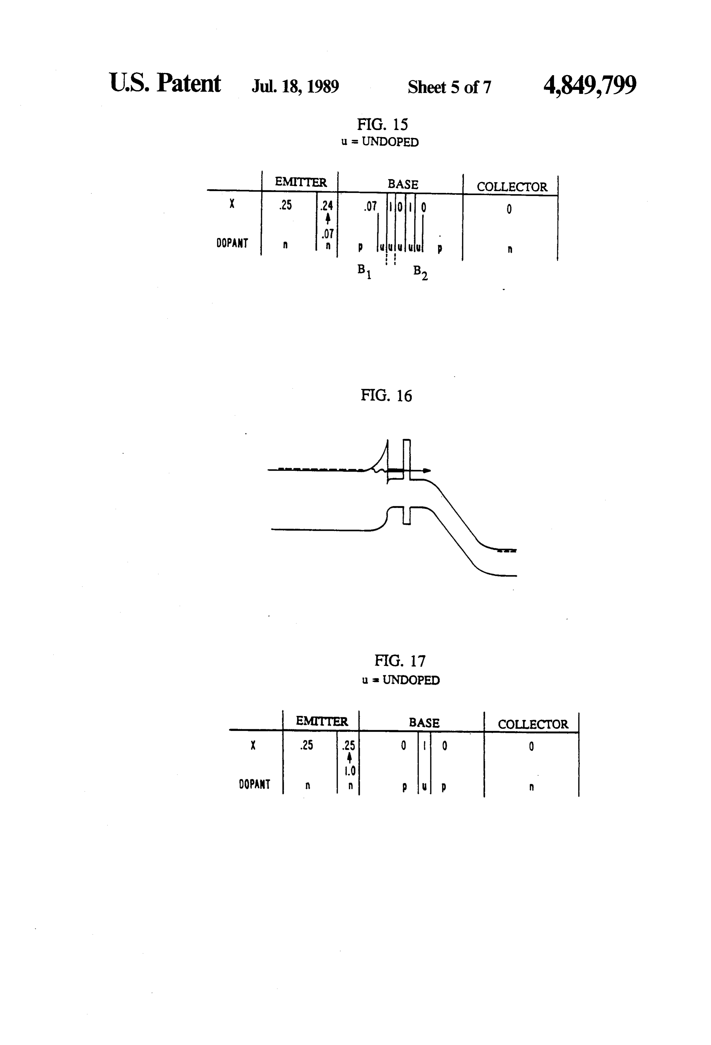
through the device is equal to the product of the trans FIG. 15 is a graphical representation of the composi mission coefficients of the two barriers without the tional make-up of a specific device of the invention, quantum well. O such representation being in correspondence with en In one embodiment, the emitter is degenerately ergy band diagrams as shown in FIG. 13A, 13B, and doped. In another embodiment, an abrupt emitter is 13C;
used, and electrons are ballistically launched into the FIG. 16 is an energy band diagram of a device under quantum states of the well. The symmetric barrier may operating conditions in which the emitter serves to be a double barrier having a square or parabolic quan 15 define one side of the quantum well in accordance with tum well. The transistor may be multiple resonances a further embodiment of the invention;
when the barrier parameters are appropriately selected FIG. 17 is graphical representation of the composi and is of utility for a variety of both signal processing tional make-up of a specific device of the invention in and logic applications. For example, some applications correspondence with FIG. 16;
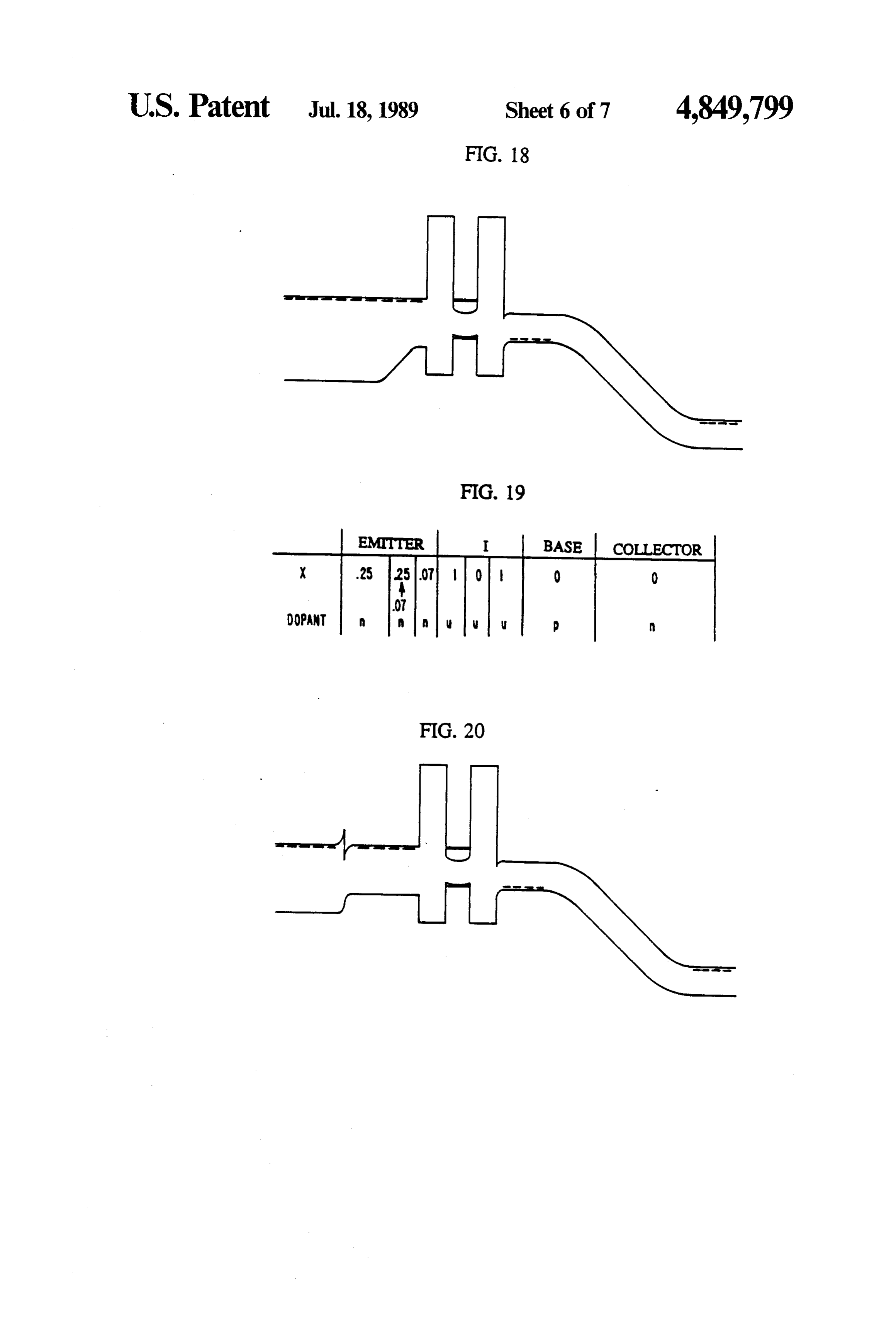
utilize the multiple-value voltage transfer characteristic. 20 FIG. 18 is an energy band diagram of a device under Other applications use the multiple-value negative resis operating conditions in which a quantum well is in a tance characteristic. region between emitter and base regions; Other embodiments of the invention do not involve FIG. 19 is a graphical representation of the composi high-energy injection of minority carriers. In one case tional make-up of a specific device of the invention in of resonant tunneling transistor operation, a bipolar correspondence with FIG. 18;
structure comprises a wide-bandgap graded emitter and FIG. 20 is an energy band diagram of a alternate a double barrier in the base region; in another, such device under operating conditions in which a quantum structure comprises an emitter with abrupt narrowing of the bandgap, and a potential barrier in the base re well is in a region between emitter and base regions; FIG. 21 is a graphical representation of the composi gion. In all cases contemplated so far, a heterostructure 30 tional make-up bipolar device has, in its base region, a composition and correspondenceofwith a specific device of the invention in
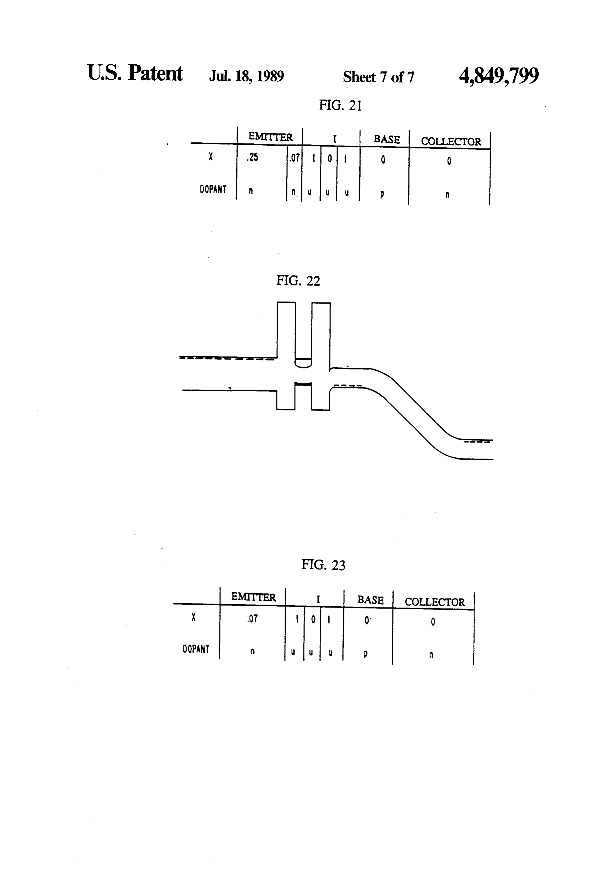
bandgap profile such that the base region has a quantum FIG. 22 is an energy band diagram of a third device well. Also, the emitter and base regions form a junction under operating conditions such that, for at least some operating condition of the in a region between emitterinandwhich base a quantum well is regions; and device, a conduction electron energy state of the quan 35
FIG. 23 is a graphical representation of the composi tum well is at or below the conduction band of the tional make-up of a specific device of the invention in emitter region, and such that the highest valence band correspondence state of the base region is above the valence band of the with FIG. 22. emitter region. DETAILED DESCRIPTION In yet another embodiment of a resonant-tunneling, 40 For reasons of clarity, the elements of the device are heterostructure bipolar transistor, a quantum well is still between emitter and collector regions, but not, as con notThe drawn to scale in the several Figures. templated above, in the base region; rather, in this em region device of FIG. 1 comprises emitter region 1, base bodiment of the invention, a quantum well is a region contacts3,7,and collector region 5. There are electrical 9, and 11 to the emitter, base, and collector intermediary to emitter and base regions. And, finally, 45 regions, respectively. The quality of these contacts is the quantum well may be doped like the emitter, the quantum well thus being located in the emitter region. increased by use of heavily doped regions 13, 15 and 17, which contact the emitter, base and collector, respec
Device operation can be characterized in terms of tively. All layers are grown on substrate 2. The emitter first, second, and third base-emitter voltages at which and collector have a first conductivity type, and the the bottom of the conduction band in at least a portion base has a second
conductivity type. The base-emitter of the emitter region is below at, and above, respec and base-collector junctions are, respectively, forward tively, a quantum resonance of the quantum well.
and reverse-biased when the device is operating. The
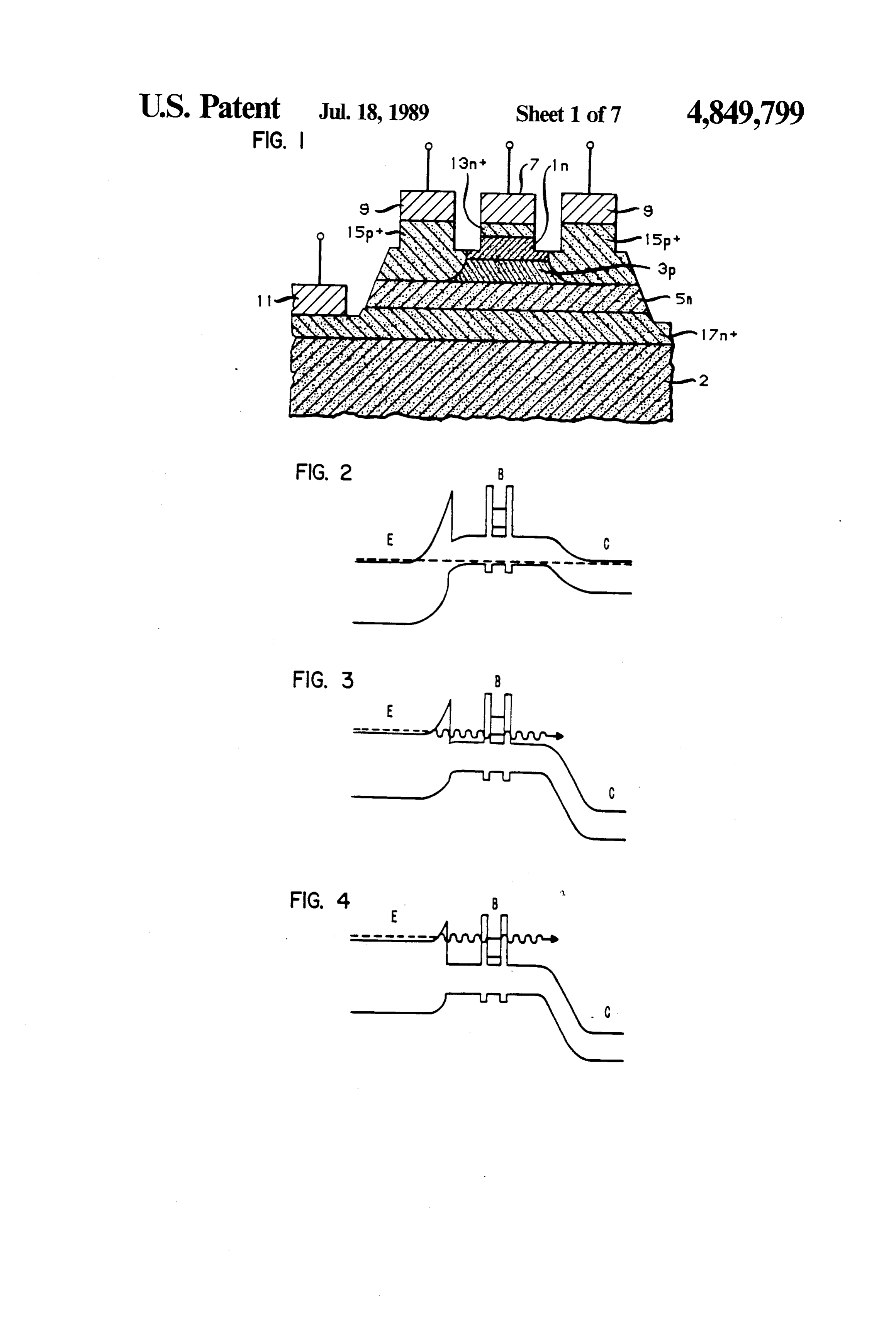
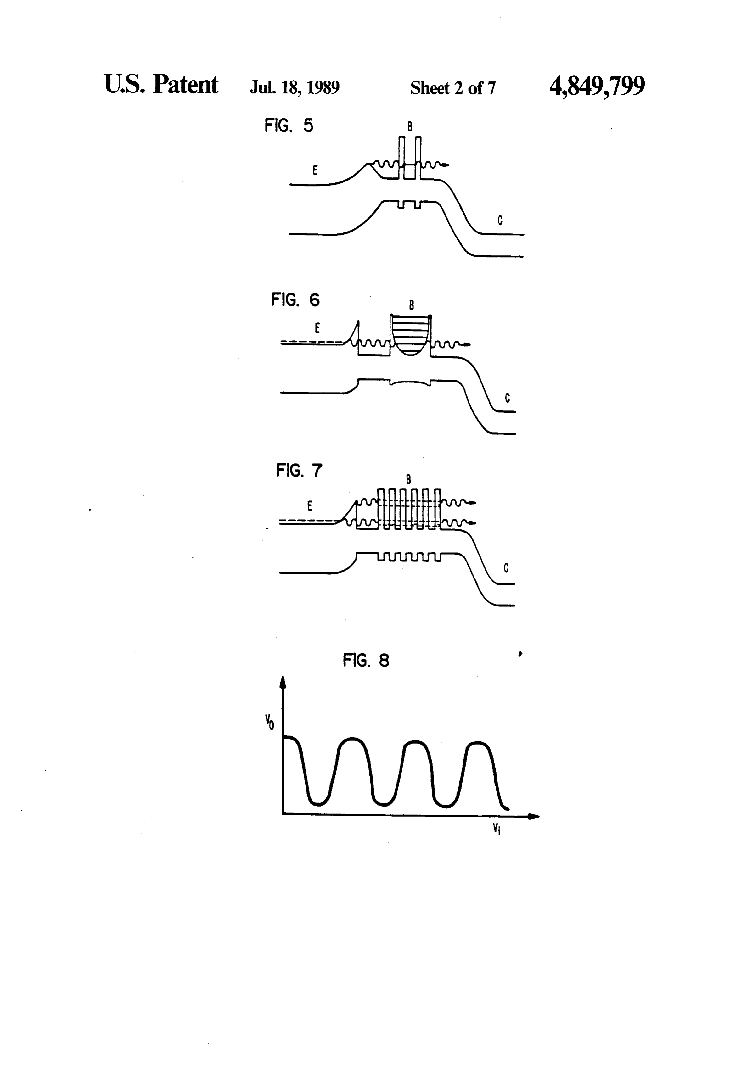
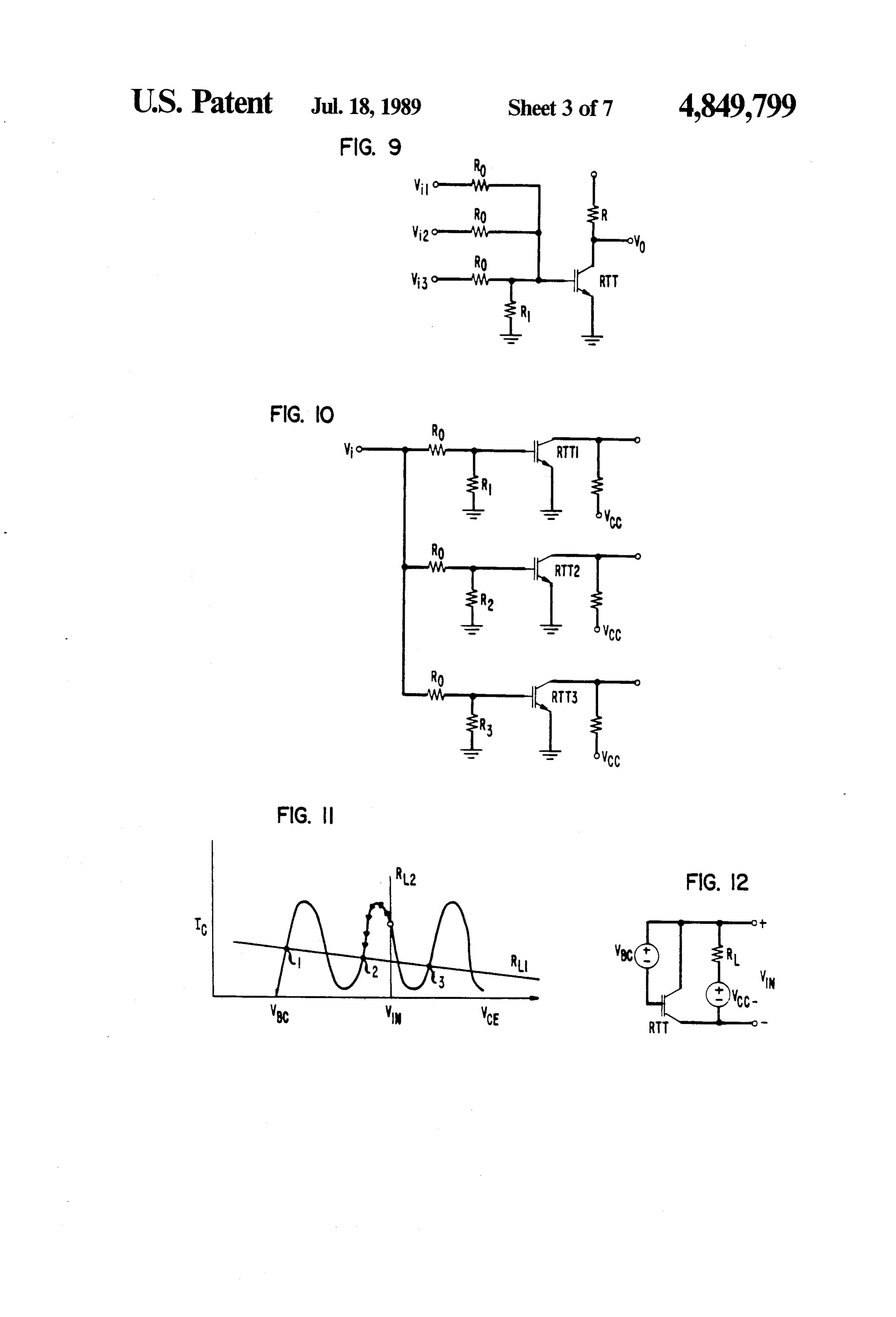
BRIEF DESCRIPTION OF THE DRAWING device is a heterojunction structure with the emitter FIG. 1 is a sectional view of a transistor according to 55 having a wider bandgap than has the portion of base this invention; region adjacent to the emitter. The heterojunction is FIGS. 2-7 are the energy band diagrams for several type I; i.e., the conduction and valence bands of the embodiments of this invention; narrow bandgap region are below and above, respec FIG. 8 plots the multiple-value transfer characteristic tively, those of the wide bandgap region. of a device according to this invention; 60 In one embodiment, the emitter is degenerately FIG. 9 is a parity generator circuit according to this doped, i.e., the Fermi level is in the conduction band. invention; The base region comprises at least one potential quan FIG. 10 is a circuit diagram of an analog-to-digital tum well which may be formed by, for example, a sym converter according to this invention; metric double barrier in the base region, although other FIG. 11 plots the current-voltage characteristic for a 65 embodiments are contemplated and will be discussed. A device according to this invention; quantum well is a potential well having discrete energy FIG. 12 is a circuit diagram of a device having a eigenstates, i.e., the allowed energy levels do not form a plurality of stable states; continuum.
Page 11
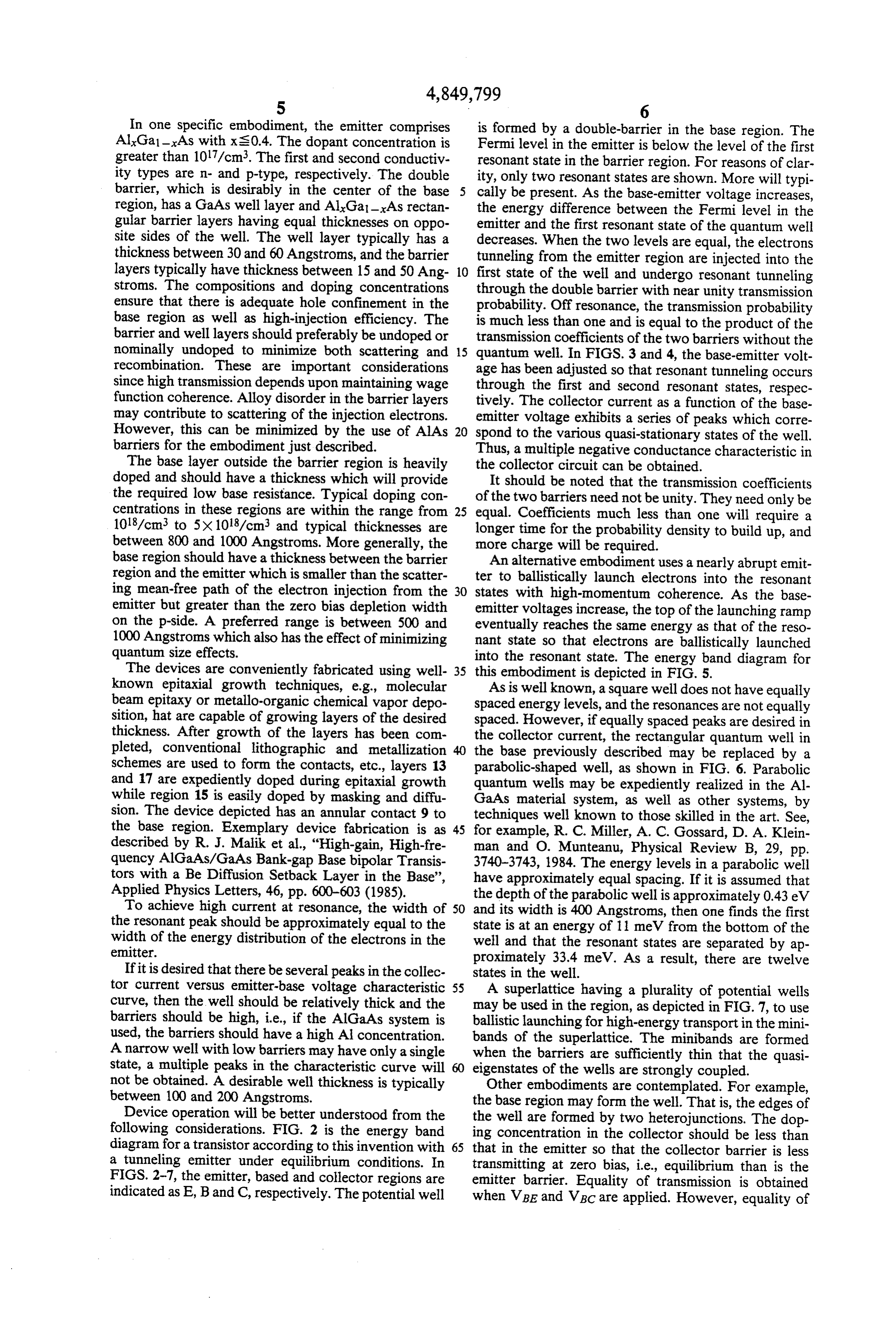
In one specific embodiment, the emitter comprises is formed by a double-barrier in the base region. The AlxGa1-xAs with xS0.4. The dopant concentration is Fermi level in the emitter is below the level of the first greater than 1017/cm3. The first and second conductiv resonant state in the barrier region. For reasons of clar ity types are n- and p-type, respectively. The double ity, only two resonant states are shown. More will typi barrier, which is desirably in the center of the base cally be present. As the base-emitter voltage increases, region, has a GaAs well layer and AlxGa1-xAs rectan the energy difference between the Fermi level in the gular barrier layers having equal thicknesses on oppo emitter and the first resonant state of the quantum well site sides of the well. The well layer typically has a decreases. When the two levels are equal, the electrons thickness between 30 and 60 Angstroms, and the barrier tunneling from the emitter region are injected into the layers typically have thickness between 15 and 50 Ang 10 first state of the well and undergo resonant tunneling stroms. The compositions and doping concentrations through the double barrier with near unity transmission ensure that there is adequate hole confinement in the probability. Off resonance, the transmission probability base region as well as high-injection efficiency. The is much less than one and is equal to the product of the barrier and well layers should preferably be undoped or transmission coefficients of the two barriers without the nominally undoped to minimize both scattering and 15 quantum well. In FIGS. 3 and 4, the base-emitter volt recombination. These are important considerations age has been adjusted so that resonant tunneling occurs since high transmission depends upon maintaining wage through the first and second resonant states, respec function coherence. Alloy disorder in the barrier layers tively. The collector current as a function of the base may contribute to scattering of the injection electrons. emitter voltage exhibits a series of peaks which corre However, this can be minimized by the use of AlAs 20 spond to the various quasi-stationary states of the well. barriers for the embodiment just described. Thus, a multiple negative conductance characteristic in The base layer outside the barrier region is heavily the collector circuit can be obtained. doped and should have a thickness which will provide It should be noted that the transmission coefficients the required low base resistance. Typical doping con of the two barriers need not be unity. They need only be centrations in these regions are within the range from 25 equal. Coefficients much less than one will require a 1018/cm3 to 5x 10¹⁸/cm3 and typical thicknesses are longer time for the probability density to build up, and between 800 and 1000 Angstroms. More generally, the more charge will be required.
base region should have a thickness between the barrier An alternative embodiment uses a nearly abrupt emit region and the emitter which is smaller than the scatter ter to ballistically launch electrons into the resonant ing mean-free path of the electron injection from the 30 states with high-momentum coherence. As the base emitter but greater than the zero bias depletion width emitter voltages increase, the top of the launching ramp on the p-side. A preferred range is between 500 and eventually reaches the same energy as that of the reso 1000 Angstroms which also has the effect of minimizing nant state so that electrons are ballistically launched quantum size effects. into the resonant state. The energy band diagram for The devices are conveniently fabricated using well 35 this embodiment is depicted in FIG. 5. known epitaxial growth techniques, e.g., molecular As is well known, a square well does not have equally beam epitaxy or metallo-organic chemical vapor depo spaced energy levels, and the resonances are not equally sition, hat are capable of growing layers of the desired spaced. However, if equally spaced peaks are desired in thickness. After growth of the layers has been com the collector current, the rectangular quantum well in pleted, conventional lithographic and metallization the base previously described may be replaced by a schemes are used to form the contacts, etc., layers 13 parabolic-shaped well, as shown in FIG. 6. Parabolic and 17 are expediently doped during epitaxial growth quantum wells may be expediently realized in the Al while region 15 is easily doped by masking and diffu GaAs material system, as well as other systems, by sion. The device depicted has an annular contact 9 to techniques well known to those skilled in the art. See, the base region. Exemplary device fabrication is as 45 for example, R. C. Miller, A. C. Gossard, D. A. Klein described by R. J. Malik et al., "High-gain, High-fre man and O. Munteanu, Physical Review B, 29, pp. quency AlGaAs/GaAs Bank-gap Base bipolar Transis 3740-3743, 1984. The energy levels in a parabolic well tors with a Be Diffusion Setback Layer in the Base', have approximately equal spacing. If it is assumed that Applied Physics Letters, 46, pp. 600-603 (1985). the depth of the parabolic well is approximately 0.43 eV To achieve high current at resonance, the width of 50 and its width is 400 Angstroms, then one finds the first the resonant peak should be approximately equal to the state is at an energy of 11 meV from the bottom of the width of the energy distribution of the electrons in the well and that the resonant states are separated by ap emitter. proximately 33.4 meV. As a result, there are twelve If it is desired that there be several peaks in the collec states in the well.
tor current versus emitter-base voltage characteristic 55 A superlattice having a plurality of potential wells curve, then the well should be relatively thick and the may be used in the region, as depicted in FIG. 7, to use barriers should be high, i.e., if the AlGaAs system is ballistic launching for high-energy transport in the mini used, the barriers should have a high A concentration. bands of the superlattice. The minibands are formed A narrow well with low barriers may have only a single when the barriers are sufficiently thin that the quasi state, a multiple peaks in the characteristic curve will eigenstates of the wells are strongly coupled. not be obtained. A desirable well thickness is typically Other embodiments are contemplated. For example, between 100 and 200 Angstroms. the base region may form the well. That is, the edges of Device operation will be better understood from the the well are formed by two heterojunctions. The dop following considerations. FIG. 2 is the energy band ing concentration in the collector should be less than diagram for a transistor according to this invention with 65 that in the emitter so that the collector barrier is less a tunneling emitter under equilibrium conditions. In transmitting at zero bias, i.e., equilibrium than is the FIGS. 2-7, the emitter, based and collector regions are emitter barrier. Equality of transmission is obtained indicated as E, Band C, respectively. The potential well when VBE and VBC are applied. However, equality of
Page 12
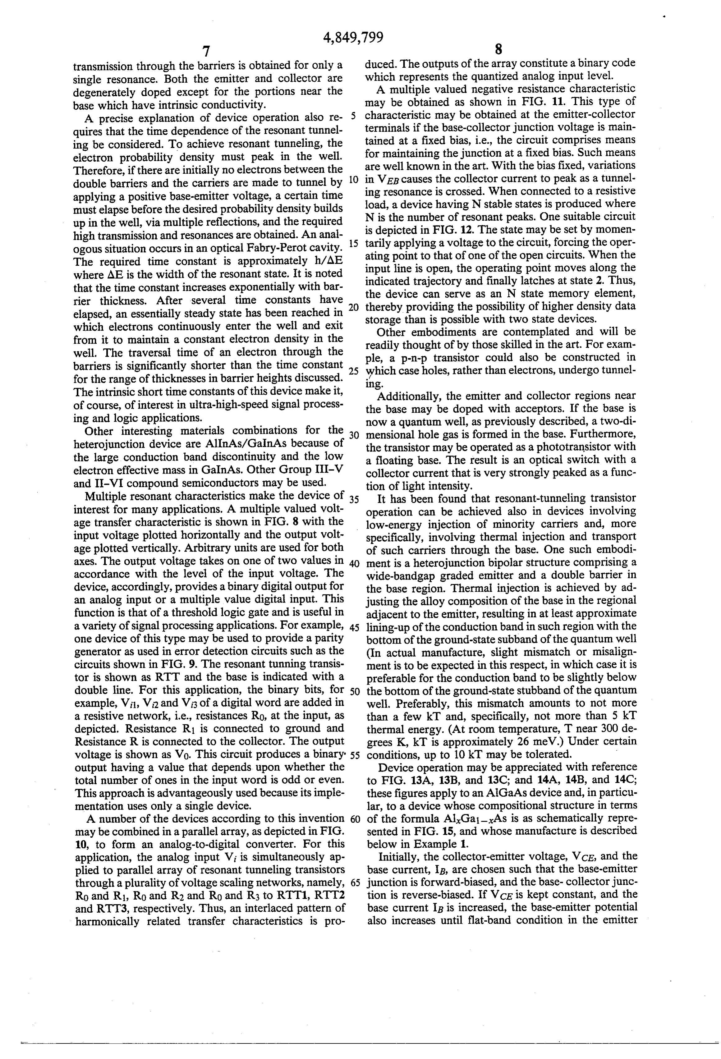
transmission through the barriers is obtained for only a duced. The outputs of the array constitute a binary code single resonance. Both the emitter and collector are which represents the quantized analog input level. degenerately doped except for the portions near the A multiple valued negative resistance characteristic base which have intrinsic conductivity. may be obtained as shown in FIG. 11. This type of A precise explanation of device operation also re- 5 characteristic may be obtained at the emitter-collector quires that the time dependence of the resonant tunnel terminals if the base-collector junction voltage is main ing be considered. To achieve resonant tunneling, the for tained at a fixed bias, i.e., the circuit comprises means electron probability density must peak in the well. maintaining the junction at a fixed bias. Such means Therefore, if there are initially no electrons between the are well known in the art. With the bias fixed, variations double barriers and the carriers are made to tunnel by 10 in VEB causes the collector current to peak as a tunnel applying a positive base-emitter voltage, a certain time ing resonance is crossed. When connected to a resistive load, a device having N stable states is produced where must elapse before the desired probability density builds N is the number of resonant peaks. One suitable circuit up in the well, via multiple reflections, and the required is depicted in FIG. 12. The state may be set by momen high transmission and resonances are obtained. An anal 15 tarily applying a voltage to the circuit, forcing the oper ogous situation occurs in an optical Fabry-Perot cavity. ating point to that
The required time constant is approximately hMAE input line is open, of one of the open circuits. When the the operating point moves along the where AE is the width of the resonant state. It is noted that the time constant increases exponentially with bar the indicated trajectory and finally latches at state 2. Thus, rier thickness. After several time constants have 20 thereby device can serve as an N state memory element, elapsed, an essentially steady state has been reached in storage than providing the possibility of higher density data which electrons continuously enter the well and exit is possible with two state devices. Other embodiments from it to maintain a constant electron density in the readily thought of by those are contemplated and will be well. The traversal time of an electron through the ple, a p-n-p transistor could skilled in the art. For exam also be constructed in barriers is significantly shorter than the time constant 25 which case holes, rather than electrons, for the range of thicknesses in barrier heights discussed. 1ng. undergo tunnel The intrinsic short time constants of this device make it, of course, of interest in ultra-high-speed signal process theAdditionally, the emitter and collector regions near base may be doped with acceptors. If the base is ing and logic applications. now a quantum well, as previously described, a two-di Other interesting materials combinations for the 30 mensional hole gas is formed in the base. Furthermore, heterojunction device are AlInAs/GanAs because of the transistor may be operated as a phototransistor with the large conduction band discontinuity and the low a floating base. The result is an optical switch with a electron effective mass in GainAs. Other Group III-V collector current that is very strongly peaked as a func and II-VI compound semiconductors may be used. tion of light intensity.
Multiple resonant characteristics make the device of is It has been found that resonant-tunneling transistor interest for many applications. A multiple valued volt operation can be achieved also in devices involving age transfer characteristic is shown in FIG. 8 with the low-energy injection of minority carriers and, more input voltage plotted horizontally and the output volt specifically, involving thermal injection and transport age plotted vertically. Arbitrary units are used for both of such carriers through the base. One such embodi axes. The output voltage takes on one of two values in 40 ment is a heterojunction bipolar structure comprising a accordance with the level of the input voltage. The wide-bandgap graded emitter and a double barrier in device, accordingly, provides a binary digital output for the base region. Thermal injection is achieved by ad an analog input or a multiple value digital input. This justing the alloy composition of the base in the regional function is that of a threshold logic gate and is useful in adjacent to the emitter, resulting in at least approximate a variety of signal processing applications. For example, 45 lining-up of the conduction band in such region with the one device of this type may be used to provide a parity bottom of the ground-state subband of the quantum well generator as used in error detection circuits such as the (In actual manufacture, slight mismatch or misalign circuits shown in FIG. 9. The resonant tunning transis ment is to be expected in this respect, in which case it is tor is shown as RTT and the base is indicated with a preferable for the conduction band to be slightly below double line. For this application, the binary bits, for 50 the bottom of the ground-state stubband of the quantum example, Vil, Vi2 and Vi3 of a digital word are added in well. Preferably, this mismatch amounts to not more a resistive network, i.e., resistances R0, at the input, as than a few kT and, specifically, not more than 5 kT depicted. Resistance R1 is connected to ground and thermal energy. (At room temperature, T near 300 de Resistance R is connected to the collector. The output grees K., kT is approximately 26 meV.) Under certain voltage is shown as Vo. This circuit produces a binary 55 conditions, up to 10 kT may be tolerated. output having a value that depends upon whether the Device operation may be appreciated with reference total number of ones in the input word is odd or even. to FIG. 13A, 13B, and 13C; and 14A, 14B, and 14C; This approach is advantageously used because its imple these figures apply to an AlGaAs device and, in particu mentation uses only a single device. lar, to a device whose compositional structure in terms A number of the devices according to this invention 60 of the formula AlxGa1-xAs is as schematically repre may be combined in a parallel array, as depicted in FIG. sented in FIG. 15, and whose manufacture is described 10, to form an analog-to-digital converter. For this below in Example 1.
application, the analog input Vi is simultaneously ap Initially, the collector-emitter voltage, VCE, and the plied to parallel array of resonant tunneling transistors base current, IB, are chosen such that the base-emitter through a plurality of voltage scaling networks, namely, 65 junction is forward-biased, and the base-collector junc R0 and R1, Ro and R2 and R0 and R3 to RTT1, RTT2 tion is reverse-biased. If VcE is kept constant, and the and RTT3, respectively. Thus, an interlaced pattern of base current IB is increased, the base-emitter potential harmonically related transfer characteristics is pro also increases until flat-band condition in the emitter
Page 13
region is reached (see FIG. 13A). In going from the In the case of an InP substrate there are two preferred band configuration of FIG. 13A to that of FIG. 13B, the major choices depending on barrier material; these are device behaves like a conventional transistor with the discussed in the following paragraphs (i) and (ii), re collector current linearly increasing with the base cur spectively.
rent (see FIG. 14A). The slope of this curve is the cur (i) The collector can be made of InP or else of Gao rent gain 3 of the device. In this region of operation, 47Ino.53As, the former being preferred in the case of electrons in the emitter overcome, by thermionic injec double heterostructure. Barriers are made of InP, and tion, the barrier of the base-emitter junction and un the quantum well of Gao.47Ino.53As, lattice matched to dergo resonant tunneling through the double barrier. If InP. For the quantum well, quaternary compounds can now the base current is further increased above the 10 also be used. The non-contacted part of the base is made value IBTH corresponding to the flat-band condition, the of InGaAsP, lattice-matched to InP. The ungraded part additional potential difference drops primarily across of the emitter is made of InP, and the graded part of the first potential barrier (see FIG. 13C) between a InGaAsP.
contact portion B2 and an uncontacted portion B of the (ii) The collector can be made either of Gao.47 Ino base because the highly doped emitter is now fully 15 53As, or of Alo.48Ino.52As, or else of InP, the latter two conducting. This pushes the conduction band edge of being preferred in the case of double heterostructure. the aluminum gallium arsenide above the first energy Barriers are made of AlO48Ino.52As, lattice-matched to level of the well, thus quenching the resonant tunneling. InP, and the quantum well of Gao.47Ino.53As, lattice The net effect is that the base transport factor and the 20 matched to InP. The non-contact part of the base is current gain are greatly reduced. This causes an abrupt made of AlInGaAs, lattice-matched to InP. The un drop of the collector current as the base current exceeds graded part of the emitter is made of Alo.48Ino.52As, and a certain threshold value IBTH (see FIG. 18). This is an theAmong graded part of AlInGaAs.
techniques suitable for the deposition of lay important manifestation of the inherent negative trans ers in structures in accordance with the invention are conductance and negative differential resistance of this 5 the following: molecular beam epitaxy (MBE), metal device. (Depending on operating point, all devices of organic chemical vapor deposition (MOCVD), vapor the invention are capable of exhibiting negative trans phase epitaxy, levitation epitaxy, and pulsed-beam mo conductance and negative differential resistance. Oper lecular beam epitaxy; with respect to the latter, see e.g., ating point depends on a number of parameters such as, M. Kawabe et al., "Composition Control e.g., the resistance between the collector and the volt 30 Ga1-xAs and New Type of Superlattice by ofPulsed Al age source and on the specific amount of the base cur Molecular Beam', Japanese Journal of Applied Phys rent.)
As illustrated by FIG. 15, the quantum well is un al., ics, Vol. 21 (1982), pp. L447-L448; and R. C. Miller et doped; alternatively, a doped quantum well may be Ga1-xAs “Parabolic Quantum Wells with the GaAs - Al advantageous in the interest of facilitating electrical 35 pp. 3740-3743. System”, Physical Review B, Vol. 29 (1984), contact. In the interest of minimized scattering, the It has been realized further that resonant-tunneling, barriers defining the quantum well are undoped. Ad heterostructure joining offset regions are optional, and they may be duced in cases inbipolar transistor operation can be pro doped or undoped. No contact is made to region B1 of base and emitter regions,aand which quantum well is in between also in cases where such the base. 40 quantum well is actually within the emitter region, the Alternatively, region B1 may be omitted altogether latter case being realized by n-doping the quantum well. as, e.g., in the case of an abrupt emitter as illustrated by Specific the band diagram shown in FIG. 16 and corresponding quantumpreferred embodiments of the case in which the compositional diagram shown in FIG. 17 relating to illustrated by energy bandbase well is between and emitter regions are diagrams presented as FIG.
AlxGa1-xAS material. This represents a variant of the 45 18, 20, and 22 in combination with corresponding com invention in which the emitter serves to define one side positional diagrams presented as FIG. 19, 21, and 23. of the quantum well in lieu of one of the potential barri As in FIG. 17, "u" stands for "undoped' in the sense ers. In this case, under operating conditions, the emitter that there is no intentional dopant addition during layer preferably is degenerately doped, and thermal injection deposition. While barrier layers are preferably un is achieved by forward-biasing. 50 doped, doping combinations as shown in Table 1 are not In all cases, the quantum well may have a non-rectan precluded. And, even in the preferred case of an un gular profile and, in particular, a parabolic profile. Also, doped well, there will be, at room temperature, a den a multiplicity of quantum wells can be used as produced sity of holes in the well which have tunneled through by a superlattice in the base region.
With respect to material systems, preferred devices of 55 the p-doped base. (In Table 1, B1 denotes the barrier region first encountered by injected carriers, W denotes the invention can be made either on GaAs or on InP the quantum well region, and B2 denotes the second substrates as follows: barrier region.) Energy band diagrams of FIG. 18, 20, In the case of GaAs, the collector is made of GaAs or and 22, as those of FIG. 2-7, 13B, and 16 apply to max AlGaAs, the latter being preferred in the case of double imum-collector-current conditions.
heterostructure. Barriers are preferably made of Al 60 The following Examples illustrate device manufac Gai-xAs, with 0.2Six S1, and the quantum well of ture and device performance, room-temperature opera GaAs which preferably is binary or essentially binary, tion as reported in Example 1 being an especially desir but with AlGaAs not precluded. The non-contacted able feature of this embodiment of the invention. part of the base is preferably made of AlGa1-As with EXAMPLE 1. ySX, the upgraded part of the emitter of AlzGa1-zAs, 65 with 0.05<zs 1, and the graded part preferably linearly A device was made by molecular beam epitaxy graded between the non-contacted part of the base and (MBE) deposition on a GaAs substrate doped n with the upgraded part of the emitter. Si. A 2100"-Angstrom GaAs buffer layer, ndoped with Si
Page 14
to 3X 10.7/cm3 carrier concentration was deposited, that of FIG. 14C was observed, which shows that heat followed by a 1.6-micrometer collector layer of GaAs, ing effects do not play a significant role. n-doped with Sito approximately 1016/cm3 carrier con The device exhibited similar behavior at other tem centration. The base layer starts with a 1900-Angstrom peratures in the range of from 100 degrees K. to 300 GaAs region adjacent to the collector, and pt-doped 5 degrees K.; the negative transconductance being with Be to approximately 1018/cm3 carrier concentra greater at lower temperatures. This is attributed to more tion; followed by a 210-Angstrom setback layer of un rapid quenching of resonant tunneling at lower temper doped GaAs. A double barrier was then grown consist atureS.
ing of a 74-Angstrom undoped GaAs quantum well When biased in the negative conductance region of sandwiched between two undoped 22-Angstrom AlAs 10 the characteristic, the device acted as an oscillator. The barriers. The last portion of the base was a 530 current oscillation in the collector circuit was picked up Angstrom layer of Alo,07Gao.93As, 105 Angstrom adja by a loop and displayed. The operating point was cent to the double barrier being undoped and the re VCE = 12 V, IB=6 mA. Oscillation was observed hav mainder p-doped with Be to approximately 1018/cm ing high spectral purity, particularly at low tempera carrier concentration. The two setback layers serve to 15 ture.
offset Be diffusion into the double barrier during high By changing the bias conditions (IB, VCE), the oscilla temperature growth at approximately 680 C. of the tion frequency could be tuned over a range of several AlGaAs graded emitter. The latter was made as a 530 megahertz. At room temperature the device ceases to Angstrom layer of AlxGa1-xAs, linearly graded from 20 oscillate for base currents less than approximately 2.5 x=0.07 to x=0.24 adjacent to the base and doped in mA because, at such currents, device operation is out with Si to approximately 3X 10.7/cm3 carrier concen side of the negative conductance region where resonant tration; and of a 3200-Angstrom layer of Alo,25Gao tunneling is not quenched; see FIG. 14C. 75As, doped n+ with Si to approximately 3X10⁷/cm3 EXAMPLE 2 carrier concentration. Finally, a 1000-Angstrom contact layer was deposited, doped in with Si to ap 25 A structure as follows represents an embodiment of proximately 3x 10¹⁸/cm3 carrier concentration, sepa the invention in accordance with FIG. 18 and 19: rate from the emitter by a 530-Angstrom region, doped A GaAs substrate (semi-insulating or doped in with n+ with Si to approximately 3X10¹⁸/cm3 carrier con Si) with a 2000-Angstrom GaAs buffer layer, n-doped centration and linearly graded from X=0.24 to x=0. 30 with Si to approximately 3x10¹⁷/cm3 carrier concen Samples having an emitter area of approximately tration;
7.5X 10.5 cm2 were made using photolithographic and a 1.5-micrometer GaAs collector layer, n-doped with wet etching techniques. The base layer was revealed by Si to approximately 5x 10¹⁶/cm3 carrier concentration anodic etching in H3PO4/H2O. The portion of the base (such thick, weakly doped layer is conveniently made, (Alo,07Gao.93As) adjacent to the emitter was also etched 35 e.g., by depositing 300 periods alternating between 1.7- away. The remainder of the base was provided with a Angstrom GaAs, n-doped with Si to approximately contact of AuBe (400 Angstroms) on Au (1100 Ang 3X 10¹⁷/cm3 carrier concentration, and 48.3-Angstrom stroms), alloyed at approximately 400 C. in a hydrogen undoped GaAs);
flow for 2 seconds. For the n-type contact to the emitter a 3000-Angstrom GaAs based layer, p-doped with Be and the collector, Au (500 Angstroms) on Sn (250 Ang to a carrier concentration in a preferred range from stroms) on Au (2000 Angstroms) was used, alloyed at 1018 to 5x 10¹⁸/cm3, optionally followed by an undoped approximately 450 C. for 1 second. GaAs offset layer which typically has a thickness in The barrier structure of this sample device is such range from 20 to 1000 Angstroms;
that the first quantized energy level is E1=65 meV, and an undoped AlAs first barrier layer which typically AEC is approximately equal to E1. Approximate equal 45 has a thickness in a range from 20 to 100 Angstroms; ity is understood in the sense that E1 does not exceed an undoped GaAs quantum well layer having a thick AEC by more than a few kT. The use of aluminum ness in a preferred range from 30 to 300 Angstroms; arsenide for the barriers is in the interest of minimizing an undoped AlAs second barrier layer which typi thermionic currents. The quantum well region was left cally has a thickness in a range from 20 to 100 Ang undoped; nevertheless, there is a high concentration 50 stroms, optionally followed by an undoped Al (approximately 7x10ll/cm2) of two-dimensional hole Ga1-xAs offset layer typically having a thickness in a gas in the well. Such holes have transferred from the range from 20 to 1000 Angstroms, where choice of nearby aluminum gallium arsenide region by tunneling composition, x, is motivated by the condition that the through the aluminum arsenide barrier, so as to achieve first quantum state, El, be equal to or exceed the con Fermi level line-up in the base. 55 duction band discontinuity between the material of the The device was tested at a temperature of approxi well and the material adjacent to the barrier first en mately 300 degrees K., and the current-voltage charac countered by injected carriers, AEC, by at most a few teristics were displayed on a tracer. For base currents kT;
IB less than or equal to 2.5 mA, the transistor exhibited a 500-Angstrom AlxGa1-xAs emitter graded layer, normal characteristics, while for IB greater than or 60 with X gradually changing across the thickness of the equal to 2.5 mA the behavior was as discussed above. layer from a value of 0.07 to a value of 0.25, and n Collector current increases in direct relationship with doped with Si to approximately 5x10¹⁷/cm3 carrier base current and there is current gain (3=7 for Ice 4 concentration (e.g., grading may be in linear or para mA). As the base current exceeds 2.5 mA there is a drop bolic fashion);
in IC due to quenching of the current gain mechanism 65 a 2000-Angstron emitter layer of Alo.25Gao.75As, by the suppression of resonant tunneling. The transistor n-doped with Si to approximately 5x10¹⁷/cm3 carrier characteristics were also measured in a pulsed mode concentration (other compositions of the form Al using 300 microsecond pulses. A behavior identical to Ga1-xAs, 0.2Sx S0.75 also represent possible emitter
Page 15
layer materials, with carrier concentration preferably in bottom of the conduction band in at least a portion a range from 5x 10¹⁶ to 1018/cm3); of said emitter region is blow, at, and above, re a 500-Angstrom AlxGa1-xAs graded layer, with X spectively, a quantum resonance of said quantum gradually changing across the thickness of the layer well, said portion being between said first electrical from the corresponding value in the emitter layer to a and said quantum well. value of 0, and n-doped with Si to approximately 2. A device as recited in claim 1 in which, at said first 3X 10¹⁸/cm3 carrier concentration; and a 3000-Angstrom GaAs contact layer, doped n with and third base-emitter voltages, the bottom of the con Si to a carrier concentration of approximately is below band duction in at least a portion of said emitter region and above, respectively, a plurality of quantum 3X10¹⁸/cm3. 10
Barrier layers can also be made of AlxGa1-xAs, resonances of said quantum well, said portion being where preferably, 0.3sxs 1. Also, barriers can be made between said first electrical contact and said quantum in the form of a superlattice, e.g., by pulsed-beam mo well.
lecular beam epitaxy as referred to above. The emitter 3. A device as recited in claim 1 in which said quan may be degenerately or nondegenerately doped. Device 15 tum well is in said emitter region. operation typically is under conditions of base-emitter 4. A device as recited in claim 1 in which said quan forward bias and base-collector reverse bias. Contact is tum well is between said emitter region and said collec to the base, and contact may also be made to the well in tor region.
the intermediary region between emitter and base (des 5. A device as recited in claim 4 in which said quan ignated “I” in FIG. 18). 20 tum well is in said base region. EXAMPLE 3 6. A device as recited in claim 4, said device compris ing a region intermediary to said emitter region and said
An embodiment of the invention in accordance with base region, and said quantum well being in said inter FIG. 20 and 21 can be viewed as obtained upon modifi mediary region.
cation of the structure of Example 2 by greater thick 25 7. A device as recited in claim 1 in which said first ness of the Alo,07Gao.93As offset layer and omission of conductivity type is n-type.
the emitter graded layer. In the interest of prevention of quantization, thickness of the offset layer is preferably tum8. well
A device as recited in claim 1 in which said quan is a parabolic well.
greater than approximately 500 Angstroms. 9. A device as recited in claim 1 in which said collec EXAMPLE 4 30 tor region and said base region form a heterojunction which is such that the conduction band of the base
An embodiment of the invention in accordance with region is below the conduction band of the collector
FIG.22 and 23 can be viewed as obtained upon modifi region, and the valence band of the base region is above cation of the structure of Example 2 by omission of the the valence band of the collector region. emitter graded layer and choice of the emitter composi 35 10. A device - tion such that El-AEC is at most a few kT. as recited in claim 9 in which the edges
TABLE 1.
of said quantum well are defined by two heterojunc tions.
B1 W B2 11. A circuit comprising a plurality of devices as recited in claim 1, and further comprising a resistive network connected to said second electrical contact, said network having a plurality of inputs.
12. A circuit comprising a plurality of devices as recited in claim 1, said devices being connected in paral
lel, further comprising a voltage scaling network, said network being connected to said second electrical
COntact.
What is claimed is: 13. A circuit comprising a device as recited in claim 1. A heterostructure bipolar device comprising: 1, further comprising means for maintaining said base an emitter region having a first conductivity type and 50 collector junction at fixed bias, and resistance con nected to said third electrical contact.
a first composition and bandgap profile; 14. A device as recited in claim 5, said device com a base region having a second conductivity type and prising means for tunneling injection of minority carri a second composition and bandgap profile;
a collector region having said first conductivity type ers into said quantum well, and said device having and having a third composition and bandgap pro 55 structure such that, for at least some operation condi file; tion, the conduction band of a portion of said base re first, second, and third electrical contracts to said gion adjoining said emitter region is essentially at the emitter, base, and collector regions, respectively; same level as the bottom of the ground-state subband of a quantum well between said collector region and said quantum well.
said electrical contact to said emitter region, said 15. A device as recited in claim 14, said portion of quantum well being the only quantum well be said base region not being electrically contacted. tween said collector region and said electrical 16. A device as recited in claim 14, said conduction contact to said emitter region. band lying below said bottom of the ground-state sub said device being capable of operating such that there band not by more than 5 kT.
are first and third base-emitter voltages and a sec 65 17. A device as recited in claim 1, said quantum well ond base-emitter voltage intermediary to said first being defined by potential barriers.
and third base-emitter voltages such that, at said 18. A device as recited in claim 17 in which said first, second, and third base-emitter voltages, the potential barriers are undoped.
Page 16
19. A device as recited in claim 17 in which said a quantum well between said collector region and quantum well is undoped. said electrical contact to said emitter region, said 20. A device as recited in claim 4, one side of said quantum well being the only quantum well be quantum well being defined by the heterojunction tween said collector region and said electrical formed by said emitter region and said base region. 5 contact to said emitter region, 21. A heterostructure bipolar photodetector device said device being capable of operating such that there comprising: are first and third base-emitter voltages and a sec an emitter region having a first conductivity type and ond base-emitter voltage intermediary to said first a first composition and bandgap profile; and third base-emitter voltages such that, at said a base region having a second conductivity type and 10 first, second, and third base-emitter voltages, the a second composition and bandgap profile; bottom of the conduction band in at least a portion a collector region having said first conductivity type of said emitter region is below, at, and above, re and having a third composition and bandgap pro- spectively, a quantum resonance of said quantum file; well, said portion being between said first electrical first, second, and third electrical contacts to said 15 contact and said quantum well. emitter, base, and collector regions, respectively; ck k it sk k
Provenance
- Collection
- Cited prior art
- Original PDF
- patentimages.storage.googleapis.com →
- Filed
- 1986-08-18
- Pages
- 16
- Method
- pdftotext (the PDF's own text layer) + pdftoppm 300dpi page scans
- Source
- Google Patents bibliographic record
- Granted
- 1989-07-18
- Inventors
- Federico Capasso; Harry T. French; Arthur C. Gossard; Albert L. Hutchinson; Richard A. Kiehl; Sustana Sen; AT&T Bell Laboratories Inc
- Transcribed from
- patentimages.storage.googleapis.com →