patent · US4590507
Variable gap devices
20 May 1986
Page 1 — bibliographic record
United States Patent (19) 11 Patent Number: 4,590,507 Capasso et al. (45) Date of Patent: May 20, 1986 54 VARIABLE GAP DEVICES 4,525,687 6/1985 Chemia et al. ............... 357/4 SL X
(75) Inventors: Federico Capasso, Westfield; Arthur OTHER PUBLICATIONS C. Gossard, Warren; Michael J.
Stavola, Westfield, all of N.J. Döhler, "Solid State Superlattices', Scientific American, (73) Assignee: AT&T Bell Laboratories, Murray Nov. 1983, pp. 144-151.
Hill, N.J. Sourcebook of Pyroelectricity, Chapter I, Sidney Lang, Gordon and Breach Co., 1974, pp. 1-47.
Primary Examiner-Martin H. Edlow 22 Filed: Jul. 31, 1984 Attorney, Agent, or Firm-Richard D. Laumann (51 Int. Cl." ...................... H01L 23/56; HO1L 27/12 (57) ABSTRACT (52) U.S. C. .......................................... 357/28; 357/4; A device having a selectively doped varying bandgap
58 Field of Search ..................... 357/4 SL, 4, 88, 28, region with pyroelectric characteristics is described 357/30, 16 which is useful as a photodetector or temperature sen
References Cited sor. A plurality of selectively doped regions forming a 56 superlattice may also be used. Ferroelectric devices are
4,348,686 9/1982 Esaki ............................ 357/4 SL X 4,353,081. 10/1982 Allyn et al. ....................... 357/88 X 19 Claims, 14 Drawing Figures
Page 2
Drawing sheet — no readable text.
Page 3
Drawing sheet — no readable text.
Page 4
Drawing sheet — no readable text.
Page 5
Drawing sheet — no readable text.
Page 6
plications include temperature sensors and memory
SUMMARY OF THE INVENTION
TECHNICAL FIELD
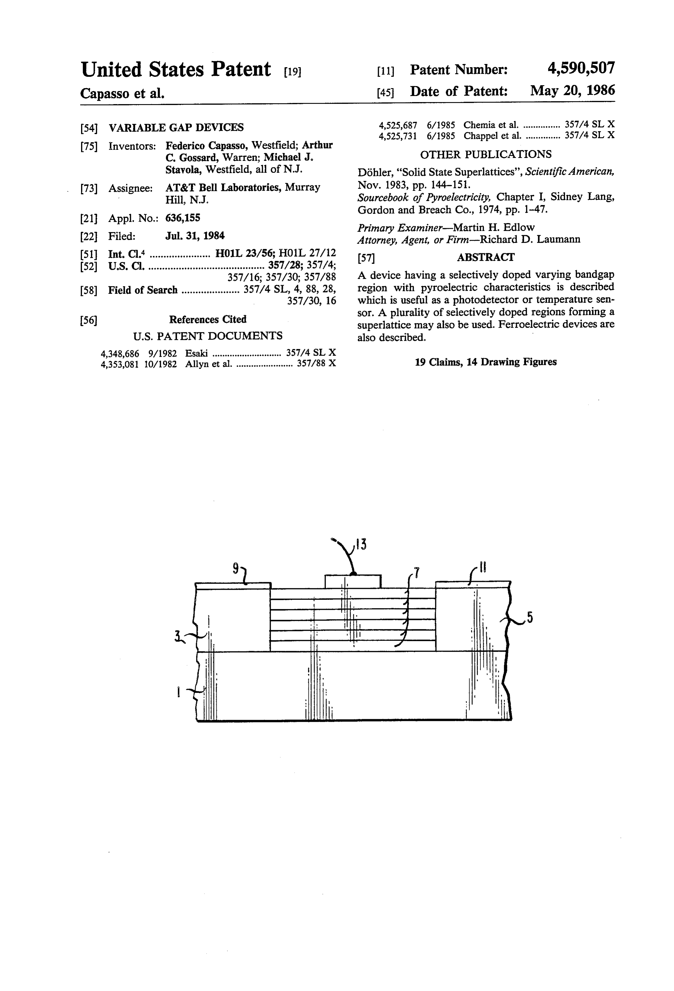
This invention relates generally to semiconductor 5 We have found that a device comprising a varying bandgap region having carriers in an asymmetric en devices and particularly to such devices having a vari ergy well has useful properties. The varying bandgap able gap structure with broken symmetry upon reflec region is in a third semiconductor region between first tion. and second semiconductor regions. The device has first BACKGROUND OF THE INVENTION 10 and second electrical contacts to said first and second regions, respectively. In particular, we have found that
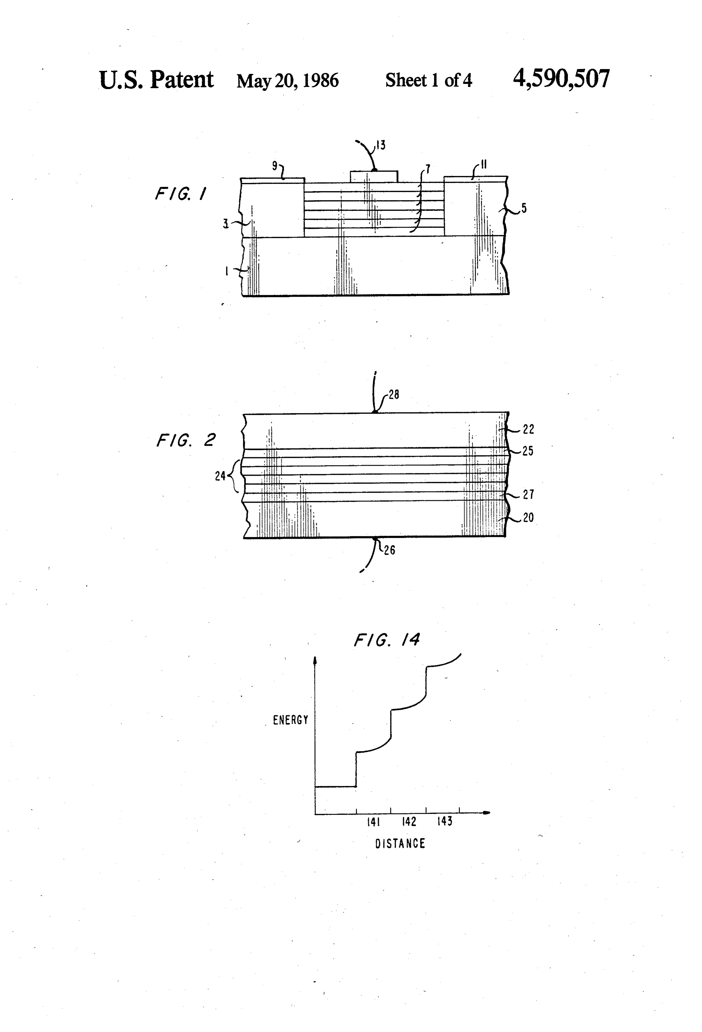
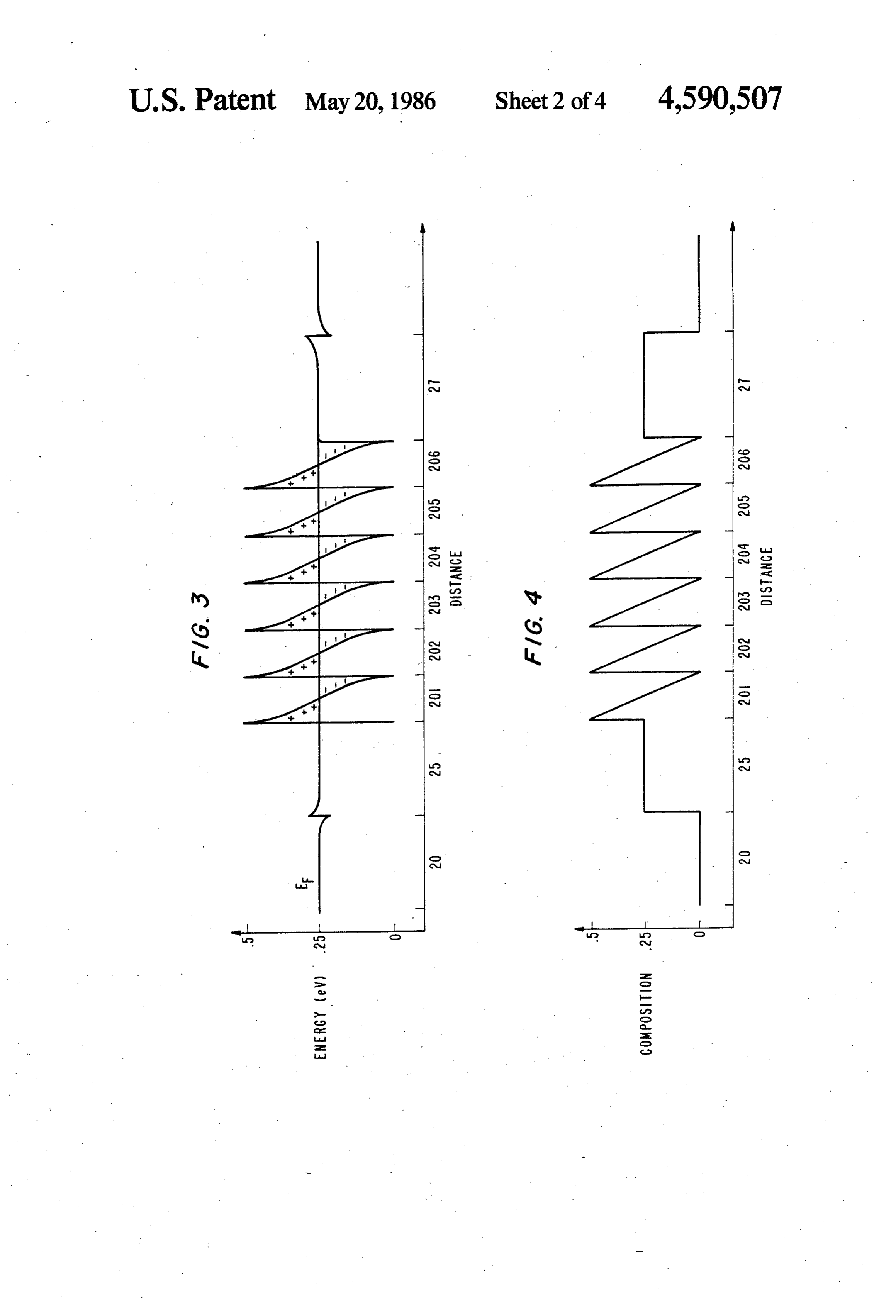
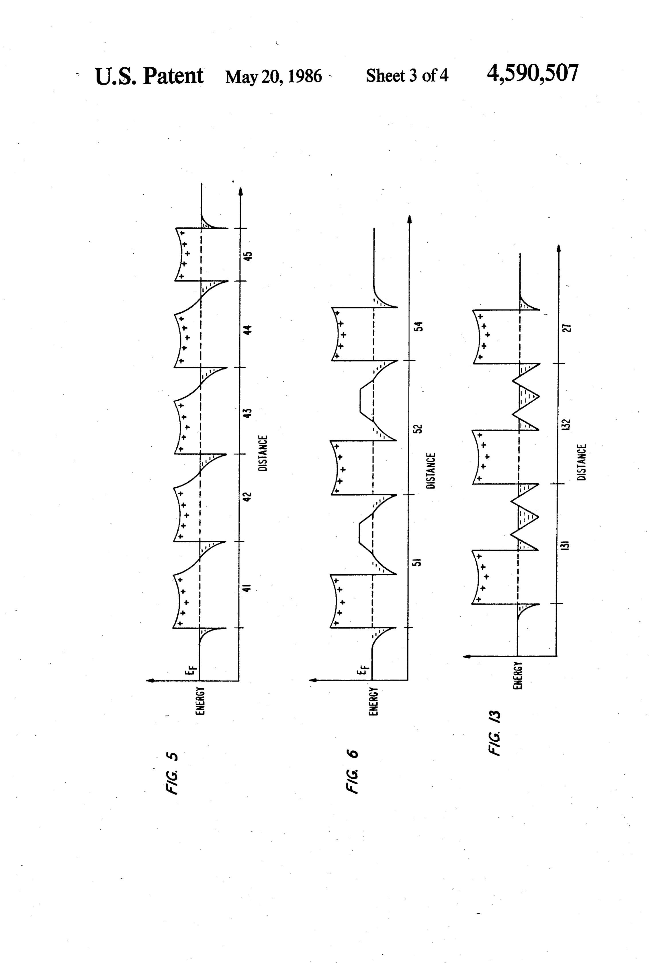
In a large number of crystals, the center of positive a device comprising a plurality of varying bandgap charge does not coincide with the center of negative regions that are selectively doped, i.e., a sawtooth charge. Such crystals are not symmetric upon reflection superlattice region has useful pyroelectric properties. and possess, in many cases, physically interesting prop 15 The third region has at least one varying bandgap re erties. For example, they may possess a spontaneous gion and is selectively doped so that the carriers and the electric polarization the magnitude of which depends dopant atoms are, energetically speaking on the aver upon the temperature of the crystal. Such crystals are age, on different sides of the Fermi level. A wide band termed pyroelectric by those skilled in the art. gap region, i.e., a confining region, provides carrier A simple physical model is usefully discussed to ex 20 confinement, i.e., the carriers are in an energy well plain the origin of pyroelectricity. Because the centers formed at the interface of the confining region and a of the negative charges and positive charges do not varying bandgap region. The well is asymmetric in a coincide, each local structural unit will have a net elec preferred embodiment. The structure exhibits a macro tric dipole. If the crystal structure is such that the elec scopic static electrical polarization because the center tric dipoles for all units do not cancel each other out, 25 of charge of the electrons does not coincide with the the structure will exhibit a spontaneous electrical polar center of charge of the ionized donors. In one preferred ization. This will happen if the orientations of the di embodiment, the varying bandgap region comprises at poles are not random, i.e., the orientations exhibit some the least one graded bandgap layer with at least a portion of degree of correlation. If the temperature of the struc 30 energy band diagram of the layer being above the ture is now increased or decreased, the strength of the in Fermi level and doped n-type. The carriers, which are dipoles is likely to change because the positions of the an asymmetric well, form a two-dimensional electron positive and negative charges with respect to each other gas below the Fermi level. It will be appreciated that vary as the charges acquire or lose thermal energy. See, some carriers may have sufficient energy to be above the Fermi level at room temperature. In another em for example, Sourcebook of Pyroelectricity, Chapter I, 35 bodiment, the carriers in the energy well are optically Sidney Lang, Gordon and Breach Co., 1974. generated by photon absorption. In some pyroelectric materials, the orientation of the electric dipoles in the crystal may be reversed by means BRIEF DESCRIPTION OF THE DRAWING of an applied external electric field. Thus, the direction FIG. 1 is a sectional view of one embodiment of our of the electrical polarization may be changed. These invention;
materials are termed ferroelectrics by those skilled in FIG. 2 is a sectional view of another embodiment of the art and form a subset of pyroelectric materials. It our invention;
will be appreciated that not all pyroelectrics have di FIG. 3 is the conduction band diagram of a pyroelec poles which can have their orientation reversed be tric superlattice device according to our invention; cause, for example, the field required for reversal might 45 FIG. 4 plots the composition in units of Al mole have a magnitude greater than the electrical breakdown fraction for a device depicted in FIG. 3; field of the material. Thus, not all pyroelectric materials FIG. 5 is the conduction band diagram of another are also ferroelectric materials. pyroelectric superlattice device according to our inven Several naturally occurring crystals are ferroelec tion;
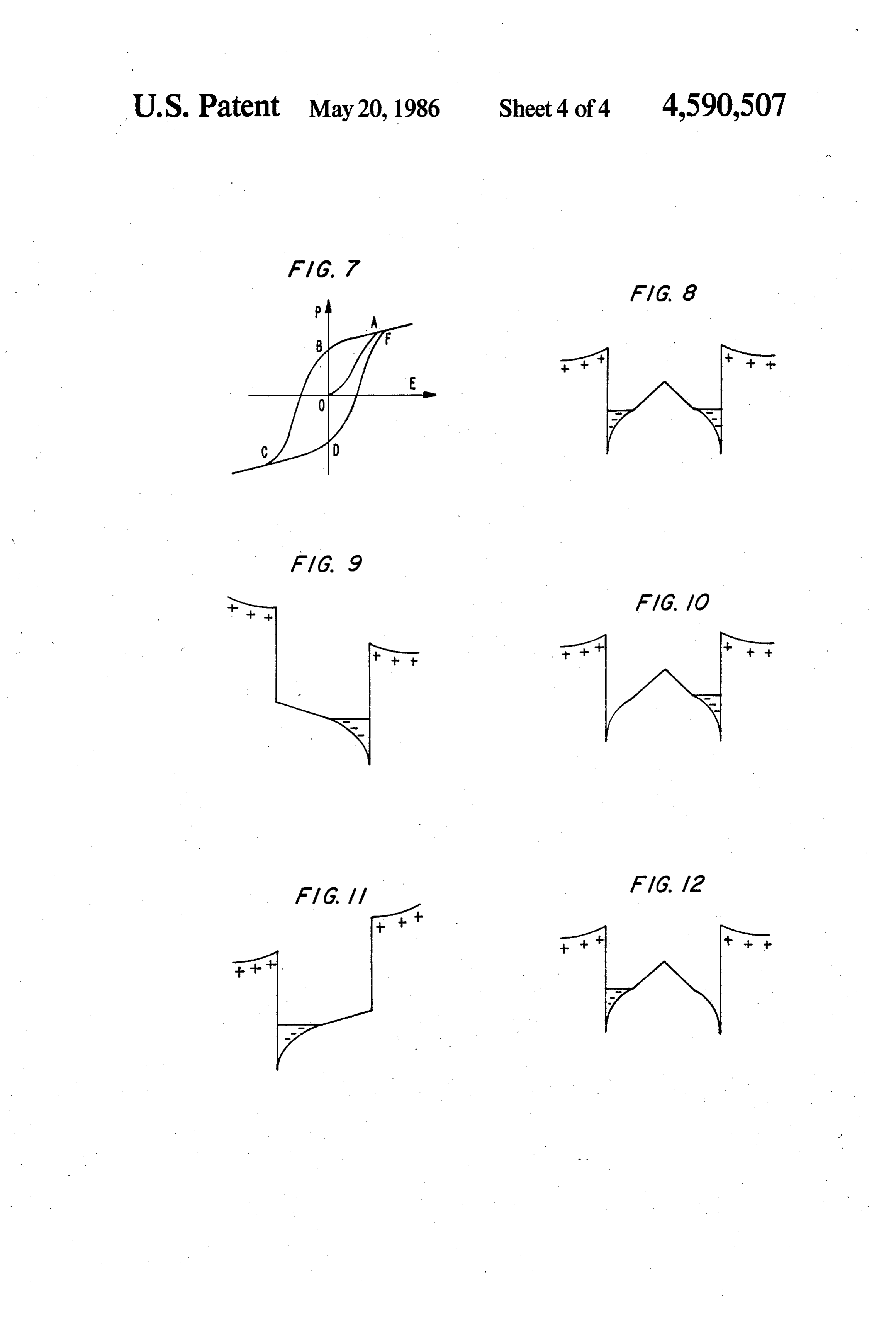
trics. First, there is Rochelle salt together with several 50 FIG. 6 is the conduction band diagram of a ferroelec chemically related salts. The origin of ferroelectricity in tric superlattice device according to our invention; these materials is believed due to the water of hydration FIG. 7 shows a hysteresis loop for an exemplary in the molecule. Second, there is a set of crystals which ferroelectric device;
includes potassium dihydrogen phosphate and related FIGS. 8-12 are conduction band diagrams of a ferro salts. The ferroelectric behavior in these materials is 55 electric superlattice device according to our invention related to the hydrogen bonds and the motion of the that is useful in explaining the polarization hysteresis associated protons. Third, there is a class of ionic crys curve in the device;
tals with either the perovskite or illemite structure. Bar FIG. 13 is the conduction band diagram of another ium titanate is an illustrative member of this class. Fer ferroelectric superlattice device according to our inven roelectric behavior is observed because the positive and tion; and negative charges are displaced with respect to each FIG. 14 is the conduction band diagram for an exem other and one type of charge has two possible lattice plary capacitor according to our invention. sites. For reasons of clarity, the elements of the devices are Ferroelectric and pyroelectric materials are thus not drawn to scale.
fairly common in nature. These materials are of com 65 DETAILED DESCRIPTION mercial interest because of their dielectric and piezo electric properties. The materials often have, for exam The structures of several embodiments of devices ple, very high dielectric constants. Other potential ap according to our invention will be described and then
Page 7
the energy band diagrams of several varying bandgap The conduction band grading depicted is conve structures useful in the devices will be discussed to niently obtained by varying the semiconductor compo explain device operation. sition. For example, AlxGa1-xAs may be used with X FIG. 1 is a sectional view of one embodiment of a varying from 0.0 to 0.5. Other semiconductors may, of pyroelectric device according to our invention. The 5 course, be used. The compositional variation in units of device comprises substrate 1, and disposed thereon, a Al more fraction is depicted in FIG. 4. The waveguid first semiconductor region 3, a second semiconductor ing regions are typically 5000 Angstroms thick and the region 5, and a third, varying bandgap, semiconductor graded bandgap regions are typically 50 to 1000 Ang region 7 which is between regions 3 and 5. Regions 3 stroms thick. If the regions are too thin, unwanted tun and 5 may have either the same or opposite conductiv 10 neling will occur between energy wells. If the regions ity types. The substrate is desirably semi-insulating or are too thick, there will not be any quantized energy insulating. The third region is a superlattice comprising States.
a plurality of regions having a varying bandgap and The regions are selectively doped with a portion of being selectively doped so that the centers of positive 15 the energy band diagram of the regions above the Fermi and negative charge do not coincide. Substrate 1 may level being n-type, that is, it has donors. Approximately also serve as a carrier confining region if there is an half of each graded bandgap region is doped n-type energy well adjacent the substrate. Regions 3, 5 and 7 with a concentration of typically between 5X10¹⁶/cm3 are electrically contacted by contacts 9, 11 and 13, to 5X10¹⁸/cm3. In general, it is desirable to have a respectively. Contacts 9 and 11 are conventional ohmic carrier 1010/cm2 density in the energy well between approxi contacts. Contact 13 may be fabricated by any of the 20 mately and approximately 1012/cm2. In the equilibrium state, the electrons from the donor conventional technologies, for example, metal-insulator atoms fill the portion of the energy band diagram of the or metal, used to fabricate gates on field effect transis conduction band below the Fermi level thus leaving a iOS,
FIG. 2 is a sectional view of another embodiment net positive charge in the portion of the structure with the conduction band above the Fermi level. The elec according to our invention. The device depicted com 25 trons prises first semiconductor region 20, second semicon dent, form a two-dimensional electron gas. As is evi ductor region 22 and a third region 24 between these with the center ofofthe the center positive charge does not coincide negative charge and the device two regions. Also present are waveguiding layers 25 thus has a net electric dipole moment and is a pyroelec and 27. The third region is similar to that in FIG. 1. 30 tric device.
Regions 20 and 22 may have either the same or opposite It will also now be appreciated that the center of conductivity type. Waveguiding regions 25 or 27 may negative charge will change as electrons are excited be omitted if desired. These regions have refractive into higher energy states. When electrons are excited, indices less than the refractive indices of the adjacent their energy states will change and because of the asym varying bandgap region. Region 27 has a bandgap 35 metric structure of the regions and the resulting energy greater than the bandgap of the adjacent portion of the wells, their average position will also change. This, of superlattice region. Region 27 may be omitted if region 20 has a larger bandgap than the adjacent superlattice course, changes the electric dipole moment and thus the net electrical polarization. The electrons may be excited region. That is, either region 20 or region 27 will be a in any of several ways such as, for example, thermal, carrier confining region. Regions 20 and 22 are electri 40 i.e., heating or cooling; optical, i.e., absorption; or elec cally contacted by contacts 26 and 28, respectively. trical, i.e., an electric field perpendicular or parallel to The regions comprise semiconductors such as Group the regions, means may be used. The internal polariza III-V compound semiconductors which are expediently tion, which is dynamically detectable, is thus modu fabricated with graded bandgaps and selective doping. lated. The devices are thus useful as temperature sen Semiconductors such as AlxGa1-xAs, AlAs, (Al-Ga1. 45 sors and photodetectors. The gate permits the electron x)yn1-yAS, GaxIn 1-xPAS1, AlxGa1-xSb, AlSb, and well shape and depth to be varied and thus varies the GaSb may be used. Hg-CdTe may also be used. The electron transport properties between regions 3 and 5. devices are expediently fabricated by, for example, The presence of a varying bandgap region in which growing the layers by molecular beam epitaxy and the electrons are confined, i.e., the asymmetric energy using conventional processing techniques. 50 well, is essential. For example, if the electrons were Our invention will be better understood by reference confined in a square or other symmetrically shaped to an exemplary energy band diagram of the third re well, their average positions will not change as they gion which forms a superlattice. For reasons of simplic receive energy and the dipole moment will not vary, ity, the energy band diagrams plot the conduction band. Alternatively, the regions may be selectively doped Unless otherwise stated, all conduction band diagrams 55 with acceptors. In such embodiments, the two dimen are depicted at Zero applied bias. Such a conduction sional gas comprises holes, which, in the energy band band diagram is depicted in FIG. 3 with the energy diagram, preferentially fill the energy band diagram plotted vertically in arbitrary units versus the distance above the Fermilevel. This type of doping will be desir normal to the superlattice regions horizontally. Six able when most of the energy bandgap difference is in superlattice regions 201, 202, 203, 204, 205 and 206 are 60 the valence band.
depicted as well as regions 25 and 27 and substrate 20. Other energy band structures are possible for the The Fermi level is indicated as EF. Although the super third region. FIG. 5 illustrates the conduction band for lattice region depicted comprises six graded bandgap yet another embodiment in which the third region com regions, it is to be understood that more or fewer re prises a superlattice with a plurality of regions. Four gions may be usefully employed in some embodiments. 65 superlattice regions 41, 42, 43, and 44 are depicted al The portion of the region with the energy band diagram though it will be understood that more or fewer may be below the Fermi level forms an energy well for elec used. Region 45 is a carrier confining region. In this trOns. embodiment, each superlattice region has a region of
Page 8
essentially constant bandgap which is doped n-type, thus possesses a hysteresis loop. If the electric field is between two adjacent graded regions. The graded again increased, the polarization moves along the curve bandgap regions comprise, for example, AlxGa1-xAs DF. It will be readily understood that such a device with a linear variation of x with distance. Again, the may be used as a memory device.
equilibrium states for the electrons are such that they The conduction band diagram depicted in FIG. 10 is are, on the average, below the Fermi level and form a of further interest for the following device application. two-dimensional electron gas which is spatially sepa If the voltage between regions 3 and 5 is increased, the rated from the donor atoms. The dip in the conduction electrons in the energy well acquire energy and move in band of the constant bandgap region arises because of the direction parallel to the superlattice region. When the space charge of the ionized donors. Thus, the center 10 they acquire sufficient energy, i.e., when the voltage is of positive charge does not coincide with the center of great enough, they will move to the adjacent well. The negative charge and the device is pyroelectric. Differ device is thus a real space electron transfer device. If ent compositional variations may be used. For example, the electron mobilities in the two wells differ, the de a parabolic compositional variation can be used. vice will exhibit negative differential resistance. FIG. 6 illustrates the conduction band diagram of a 15 FIG. 13 depicts yet another ferroelectric superlattice ferroelectric superlattice region according to our inven energy band diagram. Two superlattice regions 131 and tion. Two varying bandgap superlattice regions 51 and 132 are depicted. Region 27 is a carrier confining re 52 are depicted. Region 54 is a carrier confining region. gion. Each region has a constant bandgap region and Each region has a region of relatively constant bandgap between constant bandgap regions, a varying bandgap which is doped n-type. Between the constant bandgap 20 region having two local maxima and three local minima. regions, there is a varying bandgap region which has a The varying bandgap region is adjacent the constant maximum energy above the Fermi level and two min bandgap region of the next superlattice region. It will be ima below the Fermi level. Thus, each superlattice noted, however, that this is a tristable device as there region has two electron wells lying below the Fermi are three electron wells between the constant bandgap level between each constant bandgap region of the 25 regions and the device may be biased so that the elec superlattice structure. The resulting structure may have trons are in any of the three wells. Operation of this the direction of the net electric dipole moment reversed device is similar to that of the device depicted in FIG. by an applied electric field and is thus a ferroelectric. 10 although it will be readily understood that the hyste FIG. 7 illustrates an exemplary hysteresis loop of the resis curve is considerably more complicated. device with the electric field plotted horizontally and 30 FIG. 14 is the conduction band diagram of a saw the polarization plotted vertically. tooth superlattice under bias. Three varying bandgap This may be better understood by reference to FIGS. regions 141, 143, and 8-12 which illustrate the polarization reversal of the is inserted between a145 p-n are depicted. The superlattice junction, i.e., the first and device under the influence of an external electric field.
For reasons of simplicity, only a single superlattice 35 second semiconductor regions have opposite conduc region is depicted. The device has two wells for elec tivity types and the p-n junction is reverse biased. At a certain reverse bias voltage, the energy band trons between the constant bandgap regions. Each well diagram is initially occupied by electrons. FIG. 8 illustrates the electronsbecomes are a staircase as shown in FIG. 14. The removed from the wells and the superlat equilibrium state of the charge carriers as the device is originally fabricated, that is with no applied electric tice becomes free of carriers. This corresponds to a field. This corresponds to point O, i.e., the origin, in steep drop in device capacitance and the device may be FIG. 7. If an electric field is now applied perpendicular used as a varactor diode.
Although our invention has been described by refer to the layer and increased in magnitude, the reflection ence to embodiments using selective doping to produce symmetry of the well is broken and the structure is carriers electrically polarized as the electrons leave one well ciated that 45 in wells below the Fermi level, it will be appre and move to the second well. The polarization increases the superlattice other techniques may be used. For example, along the line OA. Eventually, above a certain value of put into wells bylayers the may be undoped and the carriers absorption of photons. Of course, the electric field, A, the polarization tends to saturate. the recombination time for electrons and holes should This situation is depicted in FIG. 9. At this point, all be greater than the time required for useful device oper electrons have moved from one well to the other well. 50 ation. Additionally, the superlattice regions may be
If the applied electric field is now reduced to zero, the uniformly energy band diagram depicted in FIG. 10 results. This doped in which case dopants on the high corresponds to point B in FIG. 7. Although the electric energy sides of the wells will transfer charges to the low field is now the same as it was in FIG. 8, it should be energy sides below the Fermi energy. Again, only one noted that there is a remenant polarization in this situa 55 varying
What bandgap layer need be present.
is claimed is:
tion. That is, the superlattice remains polarized as all the electrons remain in one well. If the electric field is now 1. A device comprising first and second semiconduc increased in the direction opposite to that depicted in tor regions, first and second electrical contacts to said FIG. 9, polarization reversal occurs, i.e., the electrons first and second regions, respectively, a third region move to the well unoccupied in FIG. 10. The polariza between said first and second semiconductor regions, tion moves along the line BC, Saturation eventually said third region comprising at least one graded band occurs and the energy band diagram depicted in FIG. gap region, a confining region adjacent said third re 11 results. Saturation occurs at point C in FIG. 7. gion, said confining region and said third region form Again, if the electric field is now reduced to zero, there ing2.aAcarrier confining energy well. device as recited in claim 1 in which said third is a remenant polarization as depicted in FIG. 12. This 65 corresponds to point D in FIG. 7. That is, the electrons region comprises a selectively doped region with the remain in one well. It will be readily appreciated by energy levels of the carriers and the dopant atoms being those skilled in the art that the ferroelectric superlattice on different sides of the Fermi level at zero applied bias.
Page 9
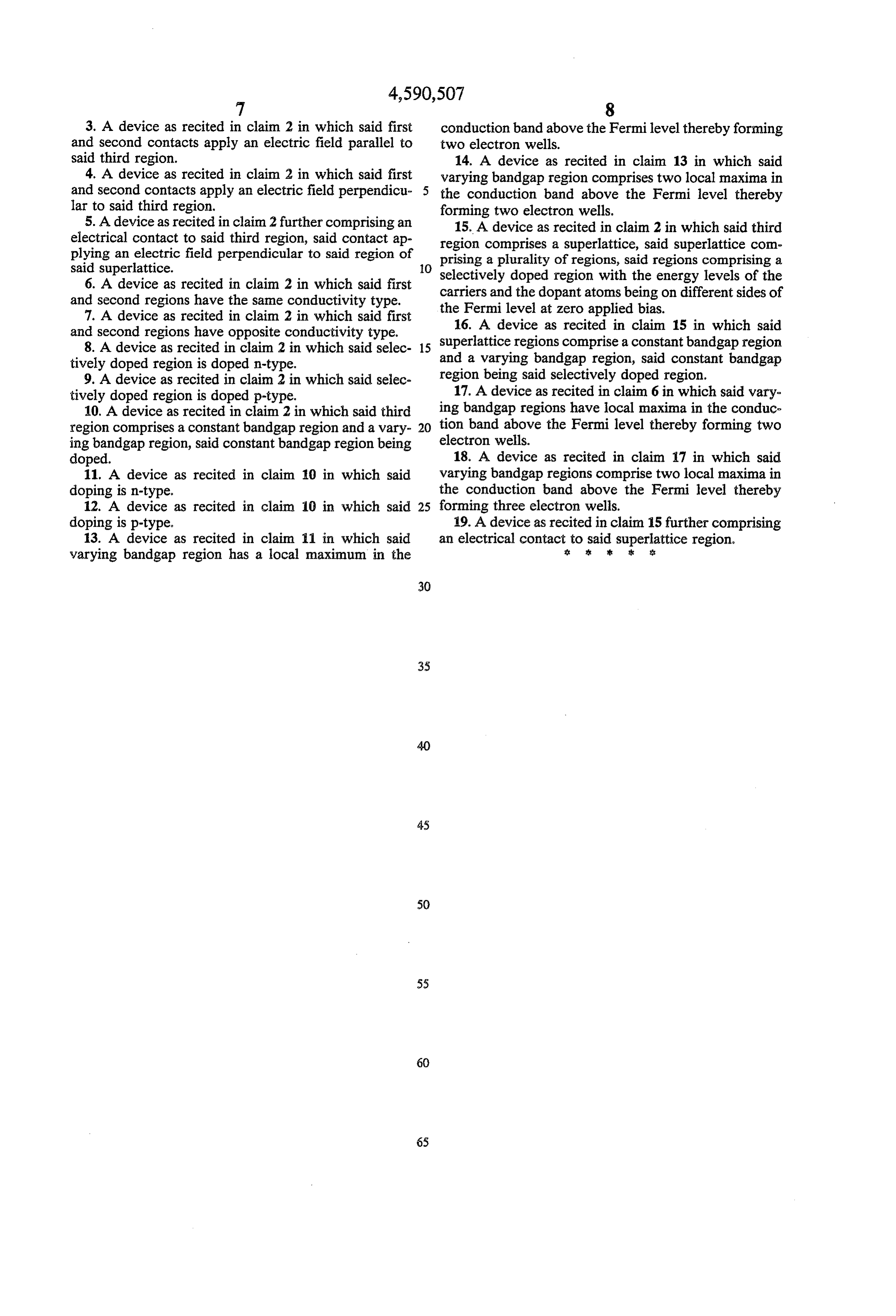
3. A device as recited in claim 2 in which said first conduction band above the Fermi level thereby forming and second contacts apply an electric field parallel to two electron wells.
said third region. 14. A device as recited in claim 13 in which said 4. A device as recited in claim 2 in which said first varying bandgap region comprises two local maxima in and second contacts apply an electric field perpendicu 5 the conduction band above the Fermi level thereby lar to said third region. forming two electron wells.
5. A device as recited in claim 2 further comprising an 15. A device as recited in claim 2 in which said third electrical contact to said third region, said contact ap region comprises a superlattice, said superlattice com plying an electric field perpendicular to said region of prising a plurality of regions, said regions comprising a
selectively doped region with the energy levels of the 6. A device as recited in claim 2 in which said first and second regions have the same conductivity type. carriers and the dopant atoms being on different sides of 7. A device as recited in claim 2 in which said first the Fermi level at zero applied bias. and second regions have opposite conductivity type. 16. A device as recited in claim 15 in which said 8. A device as recited in claim 2 in which said selec 15 Superlattice regions comprise a constant bandgap region tively doped region is doped n-type. and a varying bandgap region, said constant bandgap 9. A device as recited in claim 2 in which said selec region being said selectively doped region. tively doped region is doped p-type. 17. A device as recited in claim 6 in which said vary 10. A device as recited in claim 2 in which said third ing bandgap regions have local maxima in the conduce region comprises a constant bandgap region and a vary 20 tion band above the Fermi level thereby forming two ing bandgap region, said constant bandgap region being electron wells.
doped. 18. A device as recited in claim 17 in which said 11. A device as recited in claim 10 in which said varying bandgap regions comprise two local maxima in doping is n-type. the conduction band above the Fermi level thereby 12. A device as recited in claim 10 in which said 25 forming three electron wells.
doping is p-type. 19. A device as recited in claim 15 further comprising 13. A device as recited in claim 1 in which said an electrical contact to said superlattice region, varying bandgap region has a local maximum in the g :
Page 10
UNITED STATES PATENT AND TRADEMARK OFFICE
CERTIFICATE OF CORRECTION
INVENTOR(S) : Federico Capasso, Arthur C. Gossard and Michael J. Stavola
It is certified that error appears in the above-identified patent and that said Letters Patent is hereby corrected as shown below:
Column 5, Line 55, "remenant" should read --remnant"; Line 65, "remenant" should read-remnant--.
eigned and Sealed this
Ninth O 2 y of September 1986
SEAL
Attest:
DONALDJ. QUIGG
Attesting Officer Commissioner of attents and Trademarks
Provenance
- Collection
- Cited prior art
- Original PDF
- patentimages.storage.googleapis.com →
- Filed
- 1984-07-31
- Pages
- 10
- Method
- pdftotext (the PDF's own text layer) + pdftoppm 300dpi page scans
- Source
- Google Patents bibliographic record
- Granted
- 1986-05-20
- Inventors
- Federico Capasso; Arthur C. Gossard; Michael J. Stavola; AT&T Bell Laboratories Inc
- Transcribed from
- patentimages.storage.googleapis.com →