patent · US6232546
Microcavity apparatus and systems for maintaining a microcavity over a macroscale area
15 May 2001
Page 1 — bibliographic record
(12) United States Patent (10) Patent No.: US 6,232,546 B1 DiMatte0 et al. (45) Date of Patent: May 15, 2001
(54) MICROCAVITY APPARATUS AND SYSTEMS 5,867,990 2/1999 Ghoshal. FOR MANTAINING AMCROCAVITY 6,048,173 7/2000 DiMatteo ............................. 136/201 OVERAMACROSCALE AREA OTHER PUBLICATIONS (75) Inventors: Robert Stephen DiMatteo, Stoughton; Raynolds, J.E., Enhanced electro-magnetic energy transfer Marc Steven Weinberg, Needham; between a hot and cold body at close spacing due to Gregory A. Kirkos, Somerville, all of evanescent fields, 1999, AIP Conference Proceedings 460, MA (US) Thermophotovoltaic Generation of Electricity, Fourth NREL Conference, Denver, CO, Oct. 1998, pp. 49–57.
(73) Assignee: The Charles Stark Draper Dalvit, Diego, A.R., and Mazzitelli, Francisco D., Creation Laboratory, Inc., Cambridge, MA (US) of photons in an oscillating cavity with two moving mirrors
(*) Notice: Subject to any disclaimer, the term of this DiMatteo, R.S., Enhanced Semiconductor Carrier Genera patent is extended or adjusted under 35 tion Via Microscale Radiative Transfer. . . , Jun. 1996, U.S.C. 154(b) by 0 days. Thesis, Department of Electrical Engineering and Computer Science, Massachusetts Institute of Technology, Cambridge, (21) Appl. No.: 09/426,542 Massachusetts, pp. 1-86 and 157-162. Whale, M.D., A Fluctuational Electrodynamic Analysis of (22) Filed: Oct. 25, 1999 Microscale Radiative Transfer and the Design of Microscale Thermophotovoltaic Devices, Jun. 1997, PhD Thesis,
Related U.S. Application Data Department of Mechanical Engineering, Massachusetts Institute of Technology, Cambridge, Massachusetts.
(63) Continuation-in-part of application No. 08/902,817, filed on Wu, Ying, Chu, M.C., and Lueng P.T., Dynamics of the Jul. 30, 1997, now Pat. No. 6,084,173. quantized radiation field in a cavity vibrating at the funda mental frequency, Physical Review, vol. 59, No. 4 (Apr.
(51) Int. Cl. .......................... H01L 31/058; H01L 35/00 1999).
(52) U.S. Cl. .......................... 136/253; 136/201; 136/200;
310/306; 438/57; 438/73; 438/90 * cited by examiner (58) Field of Search ..................................... 136/253, 201, Primary Examiner Alan Diamond 136/200; 310/306; 438/57, 73, 90 (74) Attorney, Agent, or Firm-andiorio & Teska (56) References Cited (57) ABSTRACT
cavity Spacing over a macroscopic area. An application of 4,128,732 12/1978 Kaplow et al. . this invention is a microScale generator. This microScale 4,667,126 5/1987 Fitzpartick ........................... 3.10/306 generator includes a first element for receiving energy; a 4,776,895 10/1988 Goldstein. Second element, opposite the first element for transferring
5,571,339 11/1996 Ringel et al.. energy; at least one panel on either of the first element or the 5,605,171 2/1997 Tam. Second element, the panel facing the other element; a device 5,611,870 3/1997 Horne et al. . for controlling the distance between the at least one panel 5,616, 186 4/1997 Fraas et al. . and the facing element to form a predetermined, Sub-micron 5,700,332 12/1997 Brown et al.. gap between the panel and the facing element for increasing 5,753,050 5/1998 Charache et al. . energy transfer to the element for receiving, and a device, 5,769,964 6/1998 Charache et al. . responsive to the energy transfer, for generating electricity.
5,865,906 2/1999 Ferguson et al. . 37 Claims, 4 Drawing Sheets
Page 2
Drawing sheet — no readable text.
Page 3
Drawing sheet — no readable text.
Page 4
-S . S capacior
- S S
SWITCH
CIRCUIT
-4A-7- FIG. 5 MTPV System Themal Paths
a2 ; : I. S. 18 : 15 y
> Rarefied air Conduction ) Glass COnduction NY uspacer Conduction EH) Active area radiation NY standoff Conduction FIG. 6
Page 5
Drawing sheet — no readable text.
Page 6
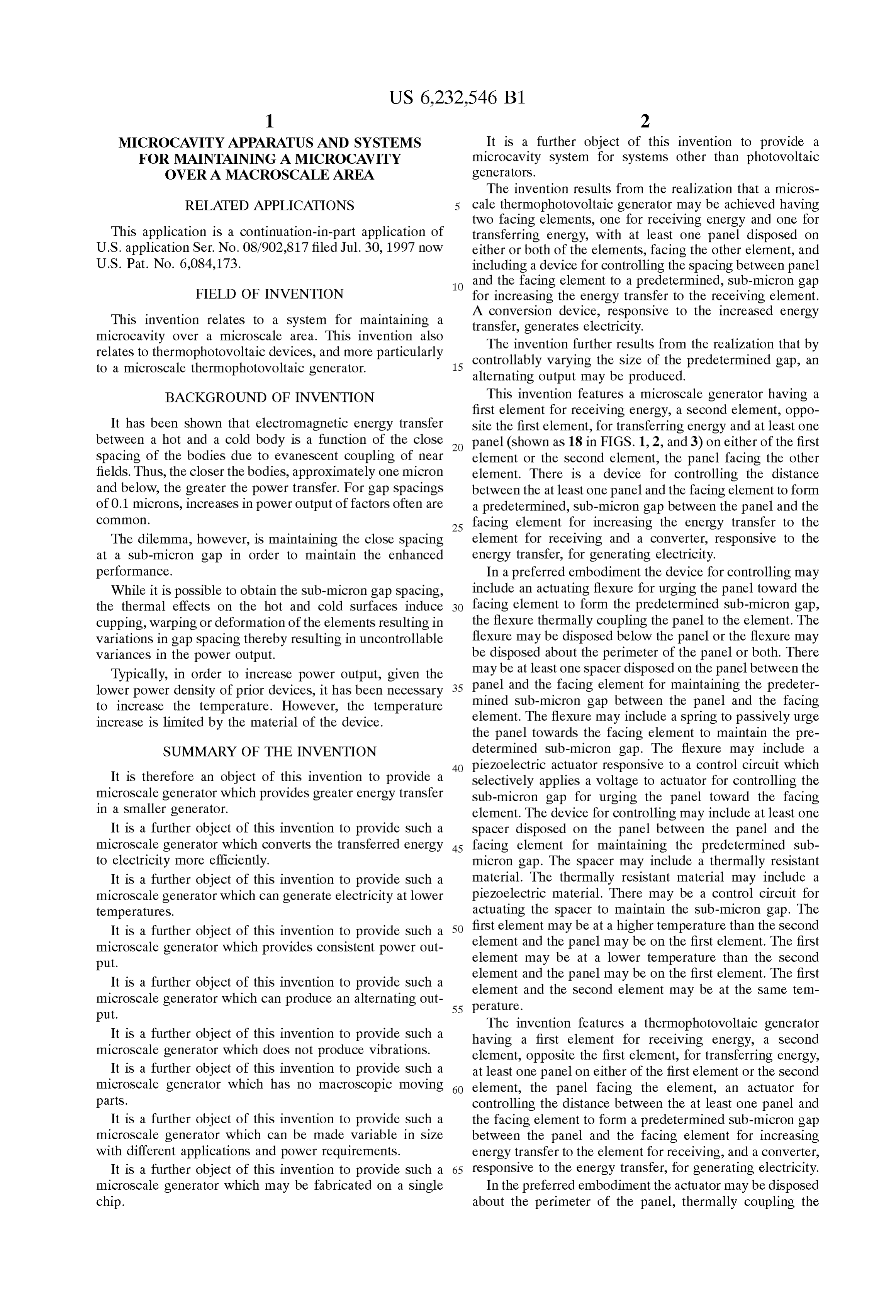
MICROCAVITY APPARATUS AND SYSTEMS It is a further object of this invention to provide a FOR MAINTAINING AMCROCAVITY microcavity System for Systems other than photovoltaic OVERAMACROSCALE AREA generatorS.
The invention results from the realization that a microS
RELATED APPLICATIONS cale thermophotovoltaic generator may be achieved having two facing elements, one for receiving energy and one for
This application is a continuation-in-part application of transferring energy, with at least one panel disposed on U.S. application Ser. No. 08/902,817 filed Jul. 30, 1997 now either or both of the elements, facing the other element, and U.S. Pat. No. 6,084,173. including a device for controlling the Spacing between panel and the facing element to a predetermined, Sub-micron gap
FIELD OF INVENTION for increasing the energy transfer to the receiving element. This invention relates to a System for maintaining a A conversion device, responsive to the increased energy transfer, generates electricity.
microcavity over a microScale area. This invention also The invention further results from the realization that by relates to thermophotovoltaic devices, and more particularly controllably varying the size of the predetermined gap, an to a microScale thermophotovoltaic generator. 15 alternating output may be produced.
BACKGROUND OF INVENTION This invention features a microScale generator having a first element for receiving energy, a Second element, oppo
It has been shown that electromagnetic energy transfer Site the first element, for transferring energy and at least one between a hot and a cold body is a function of the close panel (shown as 18 in FIGS. 1, 2, and 3) on either of the first spacing of the bodies due to evanescent coupling of near element or the Second element, the panel facing the other fields. Thus, the closer the bodies, approximately one micron element. There is a device for controlling the distance and below, the greater the power transfer. For gap spacings between the at least one panel and the facing element to form of 0.1 microns, increases in power output of factors often are a predetermined, Sub-micron gap between the panel and the 25 facing element for increasing the energy transfer to the
COO.
The dilemma, however, is maintaining the close spacing element for receiving and a converter, responsive to the at a Sub-micron gap in order to maintain the enhanced energy transfer, for generating electricity. performance. In a preferred embodiment the device for controlling may While it is possible to obtain the Sub-micron gap Spacing, include an actuating flexure for urging the panel toward the the thermal effects on the hot and cold Surfaces induce facing element to form the predetermined Sub-micron gap, cupping, warping or deformation of the elements resulting in the flexure thermally coupling the panel to the element. The variations in gap spacing thereby resulting in uncontrollable flexure may be disposed below the panel or the flexure may Variances in the power output. be disposed about the perimeter of the panel or both. There Typically, in order to increase power output, given the may be at least one Spacer disposed on the panel between the lower power density of prior devices, it has been necessary 35 panel and the facing element for maintaining the predeter to increase the temperature. However, the temperature mined Sub-micron gap between the panel and the facing increase is limited by the material of the device. element. The flexure may include a Spring to passively urge the panel towards the facing element to maintain the pre
SUMMARY OF THE INVENTION determined Sub-micron gap. The flexure may include a 40 piezoelectric actuator responsive to a control circuit which
It is therefore an object of this invention to provide a Selectively applies a Voltage to actuator for controlling the microScale generator which provides greater energy transfer Sub-micron gap for urging the panel toward the facing in a Smaller generator. element. The device for controlling may include at least one It is a further object of this invention to provide such a Spacer disposed on the panel between the panel and the microScale generator which converts the transferred energy 45 facing element for maintaining the predetermined Sub to electricity more efficiently. micron gap. The Spacer may include a thermally resistant It is a further object of this invention to provide such a material. The thermally resistant material may include a microScale generator which can generate electricity at lower piezoelectric material. There may be a control circuit for temperatures. actuating the Spacer to maintain the Sub-micron gap. The It is a further object of this invention to provide such a 50 first element may be at a higher temperature than the Second microScale generator which provides consistent power out element and the panel may be on the first element. The first put. element may be at a lower temperature than the Second It is a further object of this invention to provide such a element and the panel may be on the first element. The first microScale generator which can produce an alternating out 55 perature.and the Second element may be at the same tem element put.
The invention features a thermophotovoltaic generator
It is a further object of this invention to provide such a having a first element for receiving energy, a Second microScale generator which does not produce vibrations. element, opposite the first element, for transferring energy, It is a further object of this invention to provide such a at least one panel on either of the first element or the Second microScale generator which has no macroscopic moving 60 element, the panel facing the element, an actuator for parts. controlling the distance between the at least one panel and It is a further object of this invention to provide such a the facing element to form a predetermined Sub-micron gap microScale generator which can be made variable in size between the panel and the facing element for increasing with different applications and power requirements. energy transfer to the element for receiving, and a converter, It is a further object of this invention to provide such a 65 responsive to the energy transfer, for generating electricity. microScale generator which may be fabricated on a single In the preferred embodiment the actuator may be disposed chip. about the perimeter of the panel, thermally coupling the
Page 7
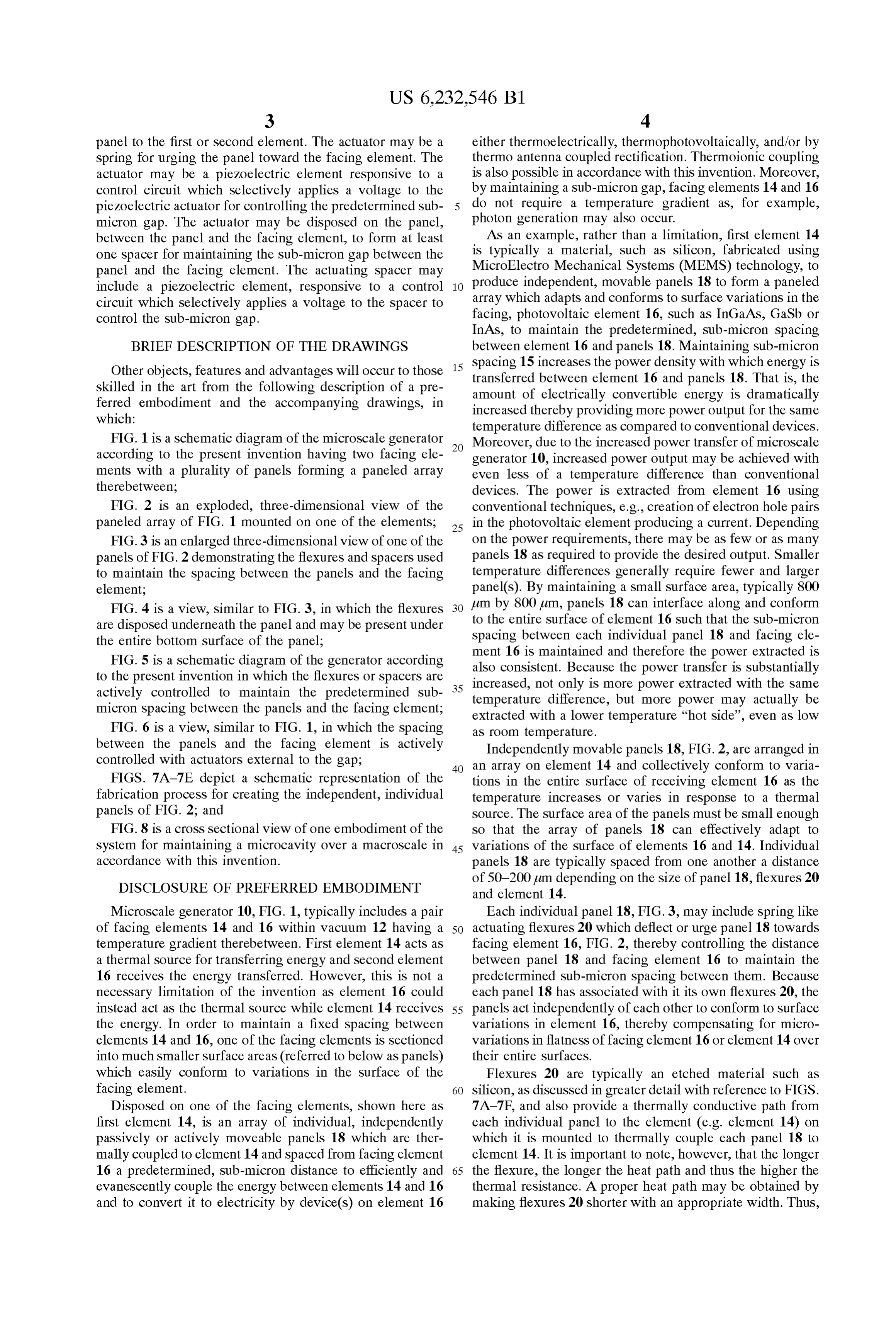
panel to the first or Second element. The actuator may be a either thermoelectrically, thermophotovoltaically, and/or by Spring for urging the panel toward the facing element. The thermo antenna coupled rectification. Thermoionic coupling actuator may be a piezoelectric element responsive to a is also possible in accordance with this invention. Moreover, control circuit which Selectively applies a Voltage to the by maintaining a Sub-micron gap, facing elements 14 and 16 piezoelectric actuator for controlling the predetermined Sub do not require a temperature gradient as, for example, micron gap. The actuator may be disposed on the panel, photon generation may also occur. between the panel and the facing element, to form at least AS an example, rather than a limitation, first element 14 one Spacer for maintaining the Sub-micron gap between the is typically a material, Such as Silicon, fabricated using panel and the facing element. The actuating Spacer may MicroElectro Mechanical Systems (MEMS) technology, to include a piezoelectric element, responsive to a control produce independent, movable panels 18 to form a paneled circuit which Selectively applies a voltage to the Spacer to array which adapts and conforms to Surface variations in the control the Sub-micron gap. facing, photovoltaic element 16, Such as InGaAS, GaSb or InAS, to maintain the predetermined, Sub-micron spacing
BRIEF DESCRIPTION OF THE DRAWINGS between element 16 and panels 18. Maintaining sub-micron Other objects, features and advantages will occur to those 15 spacing 15 increases the power density with which energy is skilled in the art from the following description of a pre amount of between transferred element 16 and panels 18. That is, the electrically convertible energy is dramatically ferred embodiment and the accompanying drawings, in increased thereby providing more power output for the same which:
temperature difference as compared to conventional devices.
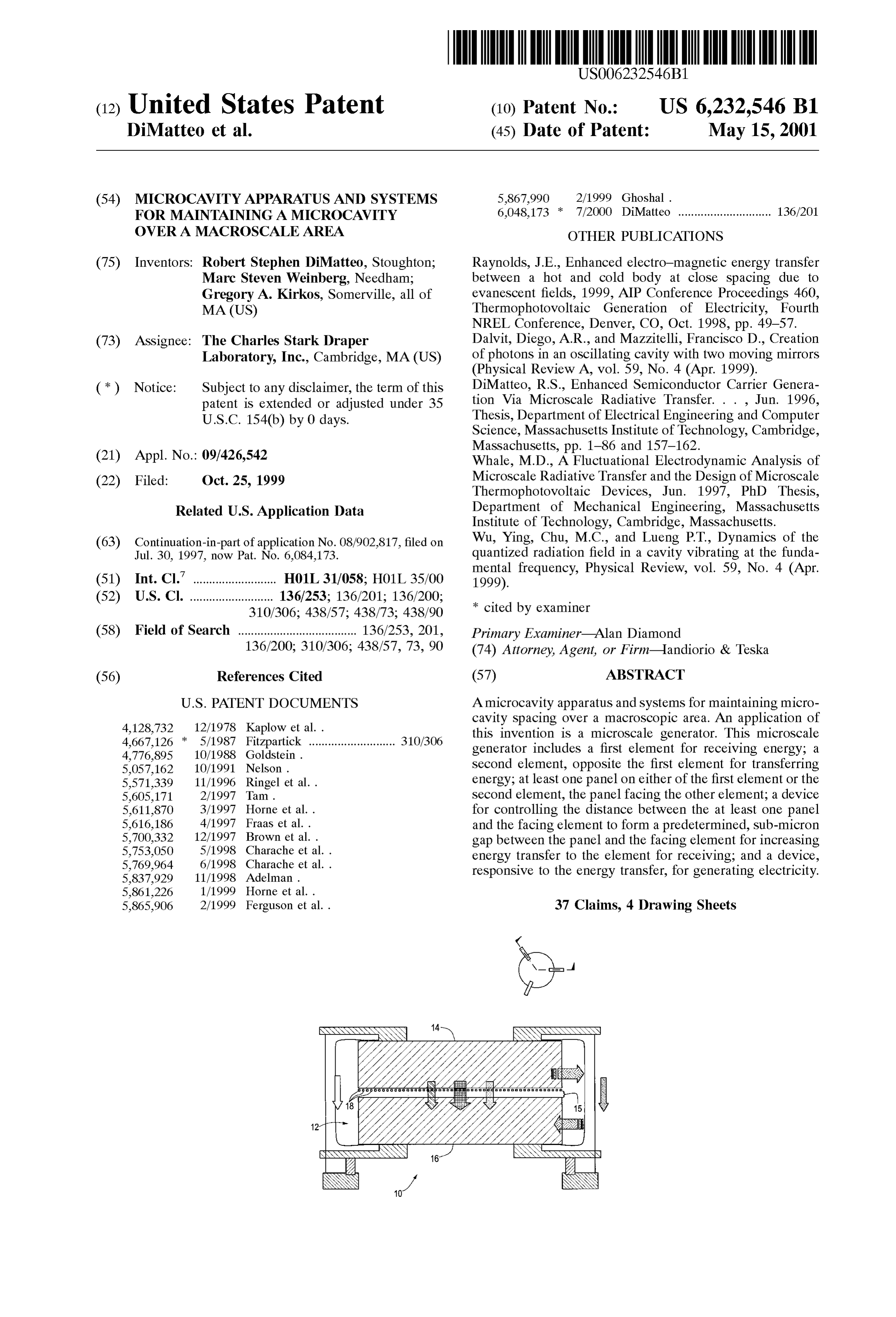
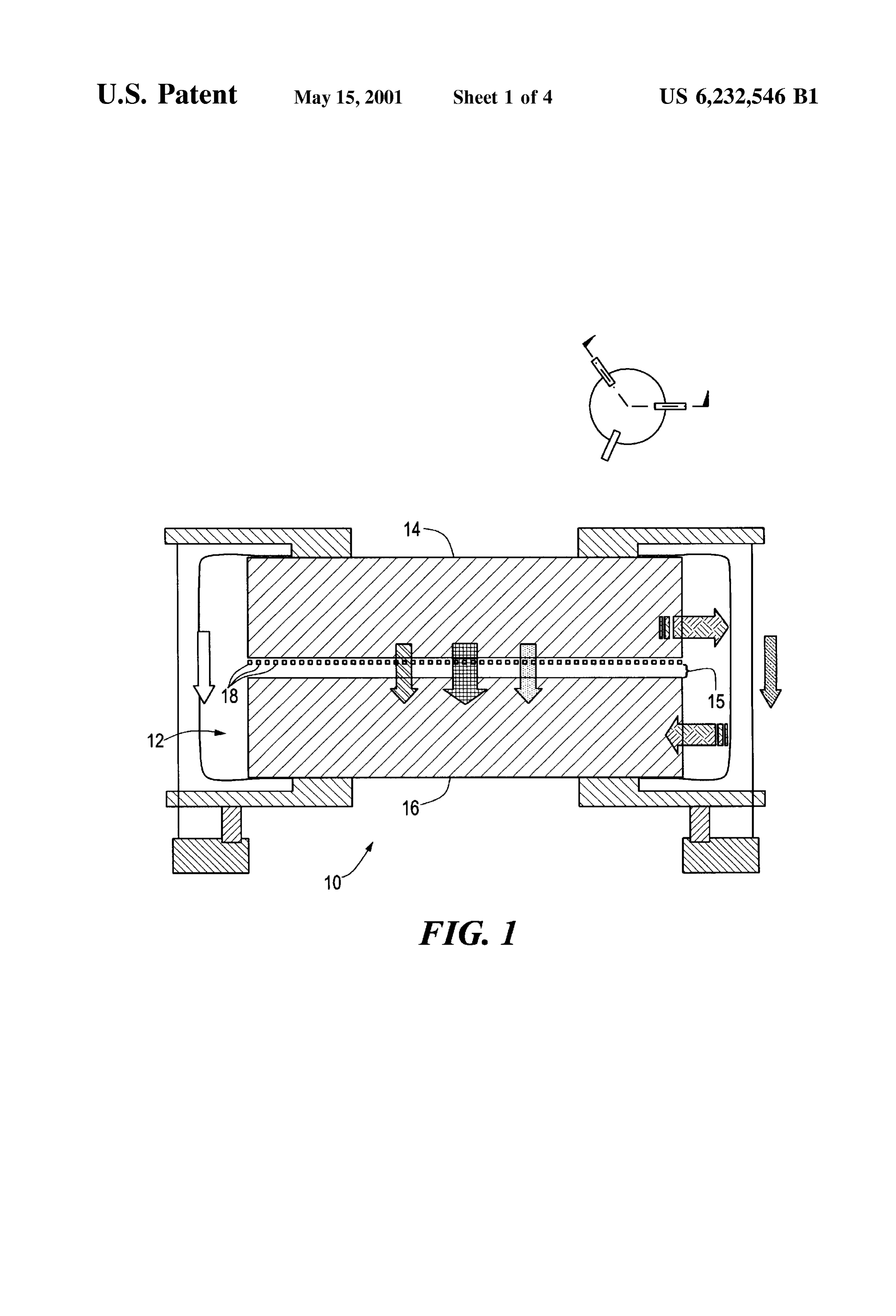
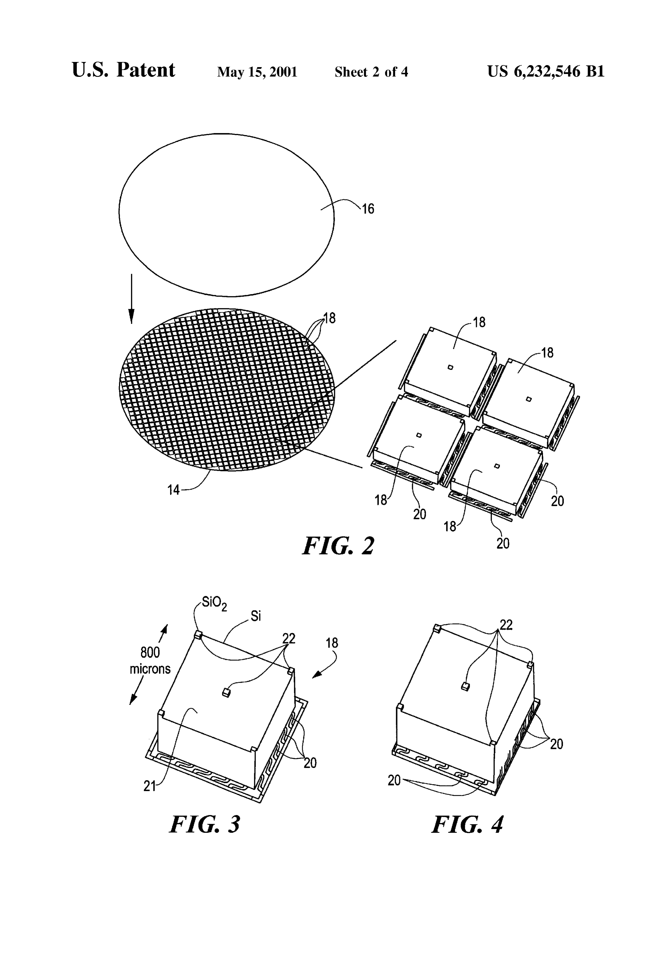
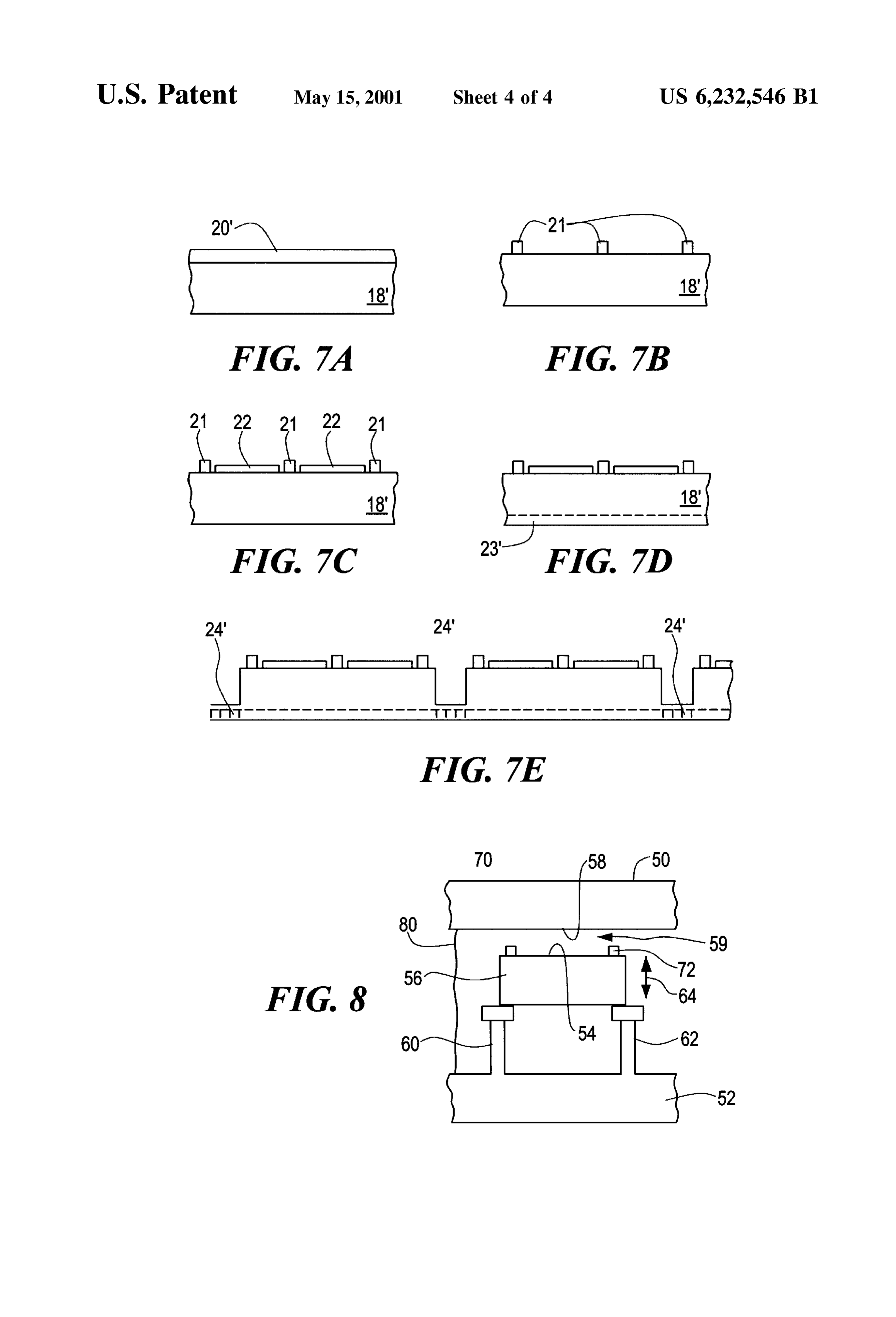
FIG. 1 is a Schematic diagram of the microScale generator Moreover, due to the increased power transfer of microScale according to the present invention having two facing ele generator 10, increased power output may be achieved with ments with a plurality of panels forming a paneled array even less of a temperature difference than conventional therebetween; devices. The power is extracted from element 16 using FIG. 2 is an exploded, three-dimensional view of the conventional techniques, e.g., creation of electron hole pairs paneled array of FIG. 1 mounted on one of the elements; 25 in the photovoltaic element producing a current. Depending FIG. 3 is an enlarged three-dimensional view of one of the on the power requirements, there may be as few or as many panels of FIG. 2 demonstrating the flexures and Spacers used panels 18 as required to provide the desired output. Smaller to maintain the spacing between the panels and the facing temperature differences generally require fewer and larger element; panel(s). By maintaining a Small Surface area, typically 800 FIG. 4 is a view, similar to FIG. 3, in which the flexures tum by 800 um, panels 18 can interface along and conform are disposed underneath the panel and may be present under to the entire Surface of element 16 Such that the Sub-micron the entire bottom Surface of the panel; spacing between each individual panel 18 and facing ele FIG. 5 is a schematic diagram of the generator according ment also 16 is maintained and therefore the power extracted is consistent. Because the power transfer is Substantially to the present invention in which the flexures or spacers are 35 increased, not only is more power extracted with the same actively controlled to maintain the predetermined Sub micron Spacing between the panels and the facing element; temperature difference, but more power may actually be extracted with a lower temperature “hot side', even as low
FIG. 6 is a view, similar to FIG. 1, in which the spacing as room temperature.
between the panels and the facing element is actively Independently movable panels 18, FIG. 2, are arranged in controlled with actuators external to the gap, 40 an array on element 14 and collectively conform to varia FIGS. 7A-7E depict a schematic representation of the tions in the entire Surface of receiving element 16 as the fabrication process for creating the independent, individual temperature increases or varies in response to a thermal panels of FIG. 2; and Source. The Surface area of the panels must be Small enough FIG. 8 is a cross sectional view of one embodiment of the so that the array of panels 18 can effectively adapt to System for maintaining a microcavity over a macroScale in 45 variations of the Surface of elements 16 and 14. Individual accordance with this invention. panels 18 are typically Spaced from one another a distance
DISCLOSURE OF PREFERRED EMBODIMENT
of 50-200 um depending on the size of panel 18, flexures 20 and element 14.
Microscale generator 10, FIG. 1, typically includes a pair Each individual panel 18, FIG. 3, may include spring like of facing elements 14 and 16 within vacuum 12 having a 50 actuating flexures 20 which deflect or urge panel 18 towards temperature gradient therebetween. First element 14 acts as facing element 16, FIG. 2, thereby controlling the distance a thermal Source for transferring energy and Second element between panel 18 and facing element 16 to maintain the 16 receives the energy transferred. However, this is not a predetermined Sub-micron Spacing between them. Because necessary limitation of the invention as element 16 could each panel 18 has associated with it its own flexures 20, the instead act as the thermal Source while element 14 receives 55 panels act independently of each other to conform to Surface the energy. In order to maintain a fixed spacing between variations in element 16, thereby compensating for micro elements 14 and 16, one of the facing elements is Sectioned variations in flatness of facing element 16 or element 14 over into much smaller Surface areas (referred to below as panels) their entire Surfaces.
which easily conform to variations in the Surface of the Flexures 20 are typically an etched material Such as facing element. 60 Silicon, as discussed in greater detail with reference to FIGS. Disposed on one of the facing elements, shown here as 7A-7F, and also provide a thermally conductive path from first element 14, is an array of individual, independently each individual panel to the element (e.g. element 14) on passively or actively moveable panels 18 which are ther which it is mounted to thermally couple each panel 18 to mally coupled to element 14 and Spaced from facing element element 14. It is important to note, however, that the longer 16 a predetermined, Sub-micron distance to efficiently and 65 the flexure, the longer the heat path and thus the higher the evanescently couple the energy between elements 14 and 16 thermal resistance. A proper heat path may be obtained by and to convert it to electricity by device(s) on element 16 making flexures 20 shorter with an appropriate width. Thus,
Page 8
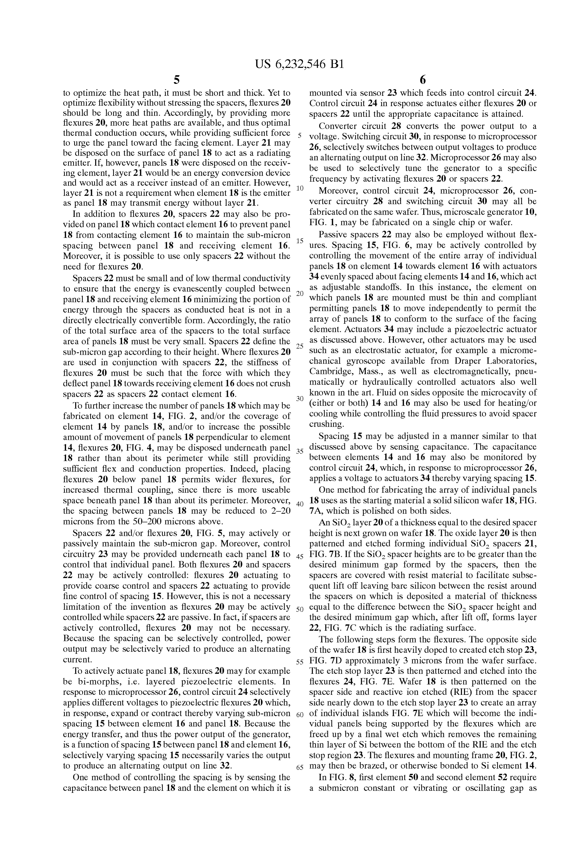
S 6 to optimize the heat path, it must be short and thick. Yet to mounted via sensor 23 which feeds into control circuit 24. optimize flexibility without Stressing the Spacers, flexures 20 Control circuit 24 in response actuates either flexures 20 or should be long and thin. Accordingly, by providing more Spacers 22 until the appropriate capacitance is attained. flexures 20, more heat paths are available, and thus optimal Converter circuit 28 converts the power output to a thermal conduction occurs, while providing Sufficient force Voltage. Switching circuit 30, in response to microprocessor to urge the panel toward the facing element. Layer 21 may 26, Selectively Switches between output voltages to produce be disposed on the Surface of panel 18 to act as a radiating an alternating output online 32. Microprocessor 26 may also emitter. If, however, panels 18 were disposed on the receiv be used to Selectively tune the generator to a specific ing element, layer 21 would be an energy conversion device frequency by activating flexures 20 or Spacers 22. and would act as a receiver instead of an emitter. However, layer 21 is not a requirement when element 18 is the emitter Moreover, control circuit 24, microprocessor 26, con as panel 18 may transmit energy without layer 21. verter circuitry 28 and Switching circuit 30 may all be In addition to flexures 20, Spacers 22 may also be pro fabricated on the same wafer. Thus, microScale generator 10, vided on panel 18 which contact element 16 to prevent panel FIG. 1, may be fabricated on a single chip or wafer. 18 from contacting element 16 to maintain the sub-micron Passive Spacers 22 may also be employed without flex spacing between panel 18 and receiving element 16. 15 ures. Spacing 15, FIG. 6, may be actively controlled by Moreover, it is possible to use only spacers 22 without the controlling the movement of the entire array of individual need for flexures 20. panels 18 on element 14 towards element 16 with actuators Spacers 22 must be small and of low thermal conductivity 34 evenly spaced about facing elements 14 and 16, which act to ensure that the energy is evanescently coupled between as adjustable Standoffs. In this instance, the element on panel 18 and receiving element 16 minimizing the portion of which panels 18 are mounted must be thin and compliant energy through the Spacers as conducted heat is not in a permitting panels 18 to move independently to permit the directly electrically convertible form. Accordingly, the ratio array of panels 18 to conform to the Surface of the facing of the total Surface area of the Spacers to the total Surface element. Actuators 34 may include a piezoelectric actuator area of panels 18 must be very small. Spacers 22 define the 25 as discussed above. However, other actuators may be used Sub-micron gap according to their height. Where flexures 20 Such as an electroStatic actuator, for example a microme are used in conjunction with Spacers 22, the Stiffness of chanical gyroscope available from Draper Laboratories, flexures 20 must be such that the force with which they Cambridge, Mass., as well as electromagnetically, pneu deflect panel 18 towards receiving element 16 does not crush matically or hydraulically controlled actuators also well Spacers 22 as Spacers 22 contact element 16. known in the art. Fluid on Sides opposite the microcavity of To further increase the number of panels 18 which may be (either or both) 14 and 16 may also be used for heating/or fabricated on element 14, FIG. 2, and/or the coverage of cooling crushing.
while controlling the fluid pressures to avoid Spacer element 14 by panels 18, and/or to increase the possible amount of movement of panels 18 perpendicular to element Spacing 15 may be adjusted in a manner Similar to that 14, flexures 20, FIG. 4, may be disposed underneath panel 35 discussed above by Sensing capacitance. The capacitance 18 rather than about its perimeter while still providing between elements 14 and 16 may also be monitored by Sufficient fleX and conduction properties. Indeed, placing control circuit 24, which, in response to microprocessor 26, flexures 20 below panel 18 permits wider flexures, for applies a voltage to actuators 34 thereby varying spacing 15. increased thermal coupling, Since there is more uSeable One method for fabricating the array of individual panels space beneath panel 18 than about its perimeter. Moreover, 40 18 uses as the starting material a solid silicon wafer 18, FIG. the spacing between panels 18 may be reduced to 2-20 7A, which is polished on both sides.
microns from the 50-200 microns above. An SiO2 layer 20 of a thickness equal to the desired spacer Spacers 22 and/or flexures 20, FIG. 5, may actively or height is next grown on wafer 18. The oxide layer 20 is then passively maintain the Sub-micron gap. Moreover, control patterned and etched forming individual SiO, Spacers 21, circuitry 23 may be provided underneath each panel 18 to 45 FIG. 7B. If the SiO spacer heights are to be greater than the control that individual panel. Both flexures 20 and spacers desired minimum gap formed by the Spacers, then the 22 may be actively controlled: flexures 20 actuating to Spacers are covered with resist material to facilitate Subse provide coarse control and Spacers 22 actuating to provide quent lift off leaving bare Silicon between the resist around fine control of Spacing 15. However, this is not a necessary the Spacers on which is deposited a material of thickness limitation of the invention as flexures 20 may be actively 50 equal to the difference between the SiO, Spacer height and controlled while Spacers 22 are passive. In fact, if Spacers are the desired minimum gap which, after lift off, forms layer actively controlled, flexures 20 may not be necessary. 22, FIG. 7C which is the radiating surface. Because the Spacing can be Selectively controlled, power The following steps form the flexures. The opposite side output may be Selectively varied to produce an alternating of the wafer 18 is first heavily doped to created etch stop 23, Current. 55 FIG. 7D approximately 3 microns from the wafer surface. To actively actuate panel 18, flexures 20 may for example The etch stop layer 23 is then patterned and etched into the be bi-morphs, i.e. layered piezoelectric elements. In flexures 24, FIG. 7E. Wafer 18 is then patterned on the response to microprocessor 26, control circuit 24 Selectively Spacer side and reactive ion etched (RIE) from the Spacer applies different Voltages to piezoelectric flexures 20 which, Side nearly down to the etch Stop layer 23 to create an array in response, expand or contract thereby varying Sub-micron 60 of individual islands FIG. 7E which will become the indi spacing 15 between element 16 and panel 18. Because the vidual panels being Supported by the flexures which are energy transfer, and thus the power output of the generator, freed up by a final wet etch which removes the remaining is a function of spacing 15 between panel 18 and element 16, thin layer of Sibetween the bottom of the RIE and the etch Selectively varying spacing 15 necessarily varies the output stop region 23. The flexures and mounting frame 20, FIG. 2, to produce an alternating output on line 32. 65 may then be brazed, or otherwise bonded to Si element 14. One method of controlling the Spacing is by Sensing the In FIG. 8, first element 50 and second element 52 require capacitance between panel 18 and the element on which it is a Submicron constant or vibrating or oscillating gap as
Page 9
defined by Surface 54 on panel 56 and Surface 58 of element 5. The microScale generator of claim 2 further including 50. See Diego, A. R.; and Mazzitelli, F. D., Creation of at least one spacing element disposed on the panel between Photons in an Oscillating Cavity with Two Moving Mirrors, the panel and the facing element for maintaining the Sub Physical Review. A vol. 59, No. 4, 1999, The American micron gap between the panel and the facing element. Physical Society; and Wu, Y. and Leung, P.T., Dynamics of 5 6. The microscale generator of claim 5 in which the Quantified Radiation Field in a Cavity Vibrating at the flexure includes and also serves as a Spring to passively urge Fundamental Frequency, Physical Review A, vol. 59., No. 4, the panel towards the facing element to maintain the Sub 1999, the American Physical Society, incorporated herein by micron gap.
this reference. 7. The microscale generator of claim 2 in which the AS Such, a number of panels 56 are disposed on Surface flexure includes a piezoelectric actuator responsive to a 52 via flexure devices 60, 62 which allow panel 56 to move control circuit which Selectively applies a Voltage to the with respect to element 52 in the direction shown by arrow actuator for controlling the Sub-micron gap. 64 to position Surface 54 at a predetermined spacing from 8. The microscale generator of claim 1 in which the device surface 58 of element 50. Also included may be protrusions for controlling includes at least one spacer disposed on the or spacers 70 and 72 for limiting spacing between surface 58 15 panel between the panel and the facing element for main and Surface 54. Thus, the subject invention is not limited to taining the Sub-micron gap.
thermophotovoltaic generators. 9. The microscale generator of claim 8 in which the spacer In a thermophotovoltaic generator, if element 50 receives includes a thermally resistant material. thermal energy, spacers 70 and 72 should be small to prevent 10. The microscale generator of claim 9 in which the heat transfer through conduction but not So Small and fragile thermally resistant material includes a piezoelectric mate that they are crushed by the flexure force of flexures 60 and rial.
62. Flexures 60 and 62 are made more flexible by making 11. The microscale generator of claim 10 further including them longer and thinner. A flexible membrane 8 may also be a control circuit for activating the Spacer to maintain the disposed between elements 50 and 52 and/or between adja Sub-micron gap.
cent elements 56 for Sealing, if required. 25 12. The microscale generator of claim 2 in which the first In Some embodiments, element 50 may be pressed against element is at a higher temperature than the Second element. spacers 70 and 72 flexing flexures 60 and 62 slightly. 13. The microscale generator of claim 12 in which the Flexures 60 and 62 and spacers 70 and 72 will then keep panel is on the first element.
micron or Submicron gap 54 at the desired spacing. In other 14. The microscale generator of claim 1 in which the first embodiments, flexures 70 and 72 will be rendered active to element is at a lower temperature than the Second element. compensate for dimensional changes in elements 50, 52 15. The microscale generator of claim 14 in which the and/or to create an oscillating or vibratory gap 54. panel is on the first element.
Thus, the generator of the present invention provides 16. The microScale generator of claim 1 in which the first greater power density and/or efficiency than prior devices element is at the Same temperature as the Second element. yet may be contained on a single chip or large arrayS. 35 17. A thermophotovoltaic generator comprising: Moreover, the generator may also produce an alternating a first element for receiving energy; current or run in reverse to heat or cool. a Second element, opposite the first element, for transfer Although specific features of the invention are shown in ring energy,
Some drawings and not in others, this is for convenience 40 at least one panel on either or both of the first element and only as each feature may be combined with any or all of the the Second element, the panel facing the other element; other features in accordance with the invention.
Other embodiments will occur to those skilled in the art an actuator for controlling the distance between the at least one panel and the facing element to form a and are within the following claims: Sub-micron gap between the panel and the facing What is claimed is: element for increasing energy transfer to the element
1. A microScale generator comprising: for receiving, and a first element for receiving energy; a converter, responsive to the energy transfer, for gener a Second element, opposite Said first element, for trans ating electricity.
ferring energy, 18. The thermophotovoltaic generator of claim 17 in at least one panel on either of the first element or the 50 which the actuator is disposed about the perimeter of the Second element, the panel facing the other element; panel, thermally coupling the panel to one of the first and a device for controlling the distance between the at least Second element.
one panel and the facing element to form a Sub-micron 19. The thermophotovoltaic generator of claim 18 in gap between the panel and the facing element for which the actuator is a Spring loaded flexure for urging the increasing energy transfer to the element for receiving, 55 panel toward the facing element.
and 20. The thermophotovoltaic generator of claim 17 in a converter, responsive to the energy transfer, for gener which the actuator includes a piezoelectric element respon ating electricity. Sive to a control circuit which Selectively applies a voltage 2. The microScale generator of claim 1 in which the device to the piezoelectric actuator for controlling the Sub-micron for controlling includes an actuating flexure for urging the 60 gap.
panel toward or away from the facing element to form the 21. The thermophotovoltaic generator of claim 17 in Sub-micron gap, the flexure thermally coupling the panel to which the actuator is disposed on the panel, between the the element to which the panel is attached. panel and the facing element, to form at least one Spacer for 3. The microscale generator of claim 2 in which the maintaining the Sub-micron gap between the panel and the actuating flexure is disposed below the panel. 65 facing element.
4. The microScale generator of claim 2 in which the 22. The thermophotovoltaic generator of claim 21 in flexure is disposed about the perimeter of the panel. which the actuating Spacer includes a piezoelectric element,
Page 10
responsive to a control circuit which Selectively applies a 30. A microelectro mechanical cell comprising a pair of Voltage to the Spacer to control the Sub-micron gap. juxtaposed parallel opposing planar Surfaces Separated by a 23. A System for maintaining a microcavity over a microgap of Spacing, one Surface comprising a mosaic of macroScale, the System comprising: Similar planar Silicon Surfaces each provided with Silicon a first element; dioxide protrusions at a plurality of points on each Silicon a Second element spaced from the first element; Surface, the mosaic being mounted against the other Surface an array of panels mounted on the Second element having with Said protrusions of each Silicon Surface contacting the Surfaces facing the first element defining a Sub-micron other Surface.
gap between the panel Surfaces and the first element; 31. The microelectro mechanical cell of claim 30 wherein and the Silicon Surfaces are each flexible to control the mounting a device associated with each panel which allows each against Said other Surface.
panel to move with respect to the Second element to 32. The microelectro mechanical cell of claim 30 wherein position each panel's Surface at a spacing from the first means is provided for maintaining the Surfaces at different element thereby defining a microcavity between the 15 temperatures.
first and Second elements. 33. The microelectro mechanical cell of claim 31 wherein 24. The system of claim 23 in which each panel's surface a Sensor is provided for Sensing Said spacing, and means is includes protrusions thereon which are engagable with the provided responsive to Said Sensing for varying the Spacing first element for limiting the Spacing between each panels through flexing of one or more of the Silicon Surfaces. Surface and the first element. 34. A method of constructing a microelectro mechanical 25. The system of claim 23 in which the device includes cell comprising a planar photovoltic Surface juxtaposed with flexural elements connected between at least one panel of a parallel mosaic of planar Silicon Surfaces therefrom to the array of panels and the Second element for passively define a microgap there between to provide Such a microgap maintaining the Spacing between each panel's Surface and of uniform spacing that comprises oxidizing a plurality of the first element. 25 marginal points of each Silicon Surface that is to oppose the 26. The system of claim 23 in which the device includes photovoltic Surface to grow corresponding Silicon oxide an actuator connected between at least one panel of the array protrusions from the Silicon Surfaces, and juxtaposing the of panels and the Second element for actively maintaining mosaic and photovoltic Surfaces with the Silicon oxide the Spacing between each panel's Surface and the first protrusions of each Silicon Surface resting on the opposing element. points of the juxtapose photovoltic Surface. 27. The system of claim 23 in which the first element is 35. The method of claim 34 and in which the opposing positioned to receive thermal energy. Silicon Surfaces are made compliant to flex upon Such 28. The system of claim 27 in which the second element juxtaposition.
is connected to a converter for generating electricity in 36. The method of claim 34 wherein said microgap is response to thermal energy transferred from the first element 35 evacuated.
to the panel Surfaces. 37. The method of claim 34 where the photovoltaic 29. The system of claim 23 in which the microcavity is an Surface is heated.
oscillating cavity and the device includes an actuator for moving each panel to cause oscillations in the cavity.
Provenance
- Collection
- Cited prior art
- Original PDF
- patentimages.storage.googleapis.com →
- Filed
- 1999-10-25
- Pages
- 10
- Method
- pdftotext (the PDF's own text layer) + pdftoppm 300dpi page scans
- Source
- Google Patents bibliographic record
- Granted
- 2001-05-15
- Inventors
- Robert Stephen DiMatteo; Marc Steven Weinberg; Gregory A. Kirkos; Charles Stark Draper Laboratory Inc
- Transcribed from
- patentimages.storage.googleapis.com →