patent · US6067309
Compound semiconductor light-emitting device of gallium nitride series
23 May 2000
Page 1 — bibliographic record
United States Patent (19) 11 Patent Number: 6,067,309 Onomura et al. (45) Date of Patent: May 23, 2000 54) COMPOUND SEMICONDUCTOR LIGHT FOREIGN PATENT DOCUMENTS
EMITTING DEVICE OF GALLUM NITRIDE
SERIES 3-286526 12/1991 Japan.
75 Inventors: Masaaki Onomura, Kawasaki; Primary Examiner James W. Davie Kazuhiko Itaya; Genichi Hatakoshi, Attorney, Agent, or Firm-Oblon, Spivak, McClelland, both of Yokohama, all of Japan Maier & Neustadt, P.C.
73 Assignee: Kabushiki Kaisha Toshiba, Kawasaki,
Japan There is disclosed a compound Semiconductor light-emitting device of gallium nitride Series having high reliability, which 21 Appl. No.: 08/921,693 can be operated by a low threshold current and a low operation Voltage without deterioration. The device com 22 Filed: Sep. 2, 1997 prises a p-type Semiconductor Structure having high carrier 30 Foreign Application Priority Data concentration, which can easily form a low resistance p-side electrode, and which can uniformly implant carriers to an
Sep. 6, 1996 JP Japan .................................... 8-236743 active layer highly efficiently. A p electrode contact layer (51) Int. Cl. .................................................. H01S 3/19 having Mg added thereto is used as a p-type Semiconductor 52 U.S. Cl. ................................................. 372/46; 372/45 layer. At least a Ga.In 2Al-N (X2+y2+Z2=1,0s x2, Z2s1, 0<y2s 1) Smoothing layer is formed on an active layer than 58 Field of Search .......................................... 372/46, 45 the p-type contact layer. On a Surface of the p-type contact
layer, there is formed a layered Structure having a Pt layer, and a Ti layer containing TN, and a Ti layer in order. An
p-type contact layer and the Pt layer.
5,740,192 4/1998 Hatano et al. ............................ 372/45 5,821,555 10/1998 Saito et al. ................................ 372/45 28 Claims, 10 Drawing Sheets
Pt ALLOY
p - A GON
p- GON
MQW
GON
GoN
GON
SAPPH RE SUBSTRATE
Page 2
Drawing sheet — no readable text.
Page 3
Drawing sheet — no readable text.
Page 4
Drawing sheet — no readable text.
Page 5
Drawing sheet — no readable text.
Page 6
Drawing sheet — no readable text.
Page 7
Drawing sheet — no readable text.
Page 8
Drawing sheet — no readable text.
Page 9
Drawing sheet — no readable text.
Page 10
Drawing sheet — no readable text.
Page 11
Drawing sheet — no readable text.
Page 12
COMPOUND SEMCONDUCTOR LIGHT Since the carriers cannot be uniformly implanted to the EMITTING DEVICE OF GALLUM NITRIDE active layer, it is difficult to realize the device with the low SERIES threshold current and the low operating Voltage.
BACKGROUND OF THE INVENTION
In the light-emitting device of GaN Series, Since the p-side electrode contract resistance was high, the operating Voltage
The present invention relates to a compound Semiconduc was increased. Moreover, nickel, Serving as a p-side elec tor light-emitting device of gallium nitride Series Such as trode metal, and gallium forming the p-type Semiconductor purple blue Semiconductor laser of gallium nitride Series layer, were reacted with each other, melted, and deteriorated (hereinafter called LD) or blue/green light-emitting diode of at an electrical conduction. As a result, it was difficult to gallium nitride series having high luminance (hereinafter continuously generate the laser. called LED). BRIEF SUMMARY OF THE INVENTION A conventional shortwave Semiconductor laser is improved to an extent that reading/writing of a disk can be An object of the present invention is to provide a com executed by a light source of 600 nm Zone using InCaAlP 15 pound Semiconductor light-emitting device of gallium nitrite and is already put to practical use. Series having high reliability, which can be operated by a In order to further improve recording density, shortwave low threshold current and a low operating Voltage without blue Semiconductor laser has been developed. A laser beam deterioration, by use of a compound Semiconductor Structure whose oscillation wave is short is useful to reduce a con of a p-type nitride gallium Series with a high carrier con Vergent size and to improve recording density. centration which can easily form a low resistance p-side For this reason, the compound Semiconductor device of uniformly electrode and which can implant carriers to an active layer and efficiently.
gallium nitrite series such as GaN, InCaN, GaAIN, InCaAlN has been recently considered as a material of the shortwave To attain the above object, there is provided a compound Semiconductor laser to improve the application to a high Semiconductor light-emitting device of gallium nitride Series density optical disk System. 25 having a compound Semiconductor of gallium nitride Series For example, in the Semiconductor laser using GaN Series (Ga, pound
Semiconductor light-emitting device comprising:
material, a room temperature pulse oscillation having wave length of 380 to 417 nm is confirmed. However, in the a Substrate;
Semiconductor laser using GaN Series material, a Satisfying a Semiconductor layer formed on the Substrate; characteristic cannot be obtained, a threshold Voltage for a an n-type Semiconductor layer, formed on the Semicon room temperature pulse oscillation ranges from 10 to 40V, ductor layer, having at least an n-type clad layer; and the variation of the value is large. an active layer formed on the n-type Semiconductor layer; This variation is caused by difficulty in a crystal growth a p-type semiconductor layer, formed on the active layer, of the compound Semiconductor layer of gallium nitride having at least a p-type clad layer; Series, and large device resistance. More specifically, there 35 a Smoothing layer of Ga-In, Al-N (x2+y2+Z2=1,0sX2, cannot be formed the compound Semiconductor layer of Z2s 1, 0<y2s 1) formed on the p-type Semiconductor p-type gallium nitride Series having a Smooth Surface and layer or the active layer; high carrier concentration. Moreover, Since contact resis a p-type contact layer, formed on the p-type Semiconduc tance of a p-side electrode is high, a large Voltage drop is tor layer, having Mg added thereto;
generated, So that the Semiconductor layer is deteriorated by a p-side electrode formed on the p-type contact layer; and a heat generation and a metal reaction even when the pulse oscillation is operated. In consideration of a cheating value, an n-side electrode formed on either the n-type Semicon the room temperature continuous oscillation cannot be ductor layer or a Substrate. achieved unless the threshold Voltage is reduced to less than 45 Thus, the p-type Semiconductor layer of gallium nitride 1OV. series having Mg added is formed on the GainAIN Smooth Moreover, when a current necessary to the laser genera ing layer containing at least In element, the number of tion is implanted, the high current flows locally and a carrier crystal defects Such as porous micro detectS is Small, and acceptor concentration of p-type Semiconductor layer can be cannot be uniformly implanted to an active layer, and an increased.
instantaneous breakage of the device occurs. As a result, the 50 The active layer may be a multi-quantum well Structure continuous generation of the laser cannot be achieved.
Thus, to realize the purple blue Semiconductor laser of having well layers formed of at least Gaan, AlaN (x3+ gallium nitride Series having high reliability, which is oper y3+Z3=1, 0sX3, y3, Z3s 1), and barrier layers, formed ated by the low threshold current to be used in the optical tively Ga, In, Al-N (x4+y4+Z4=1, 0s x4, y4, Z4s 1), alterna layered.
disk and the low threshold Voltage, the following points are 55 As this time, the Gaan, Al-N Smoothing layer is important: formed to be thicker than the thickness of the well layer Specifically, the efficient and uniform implantation of the when In composition y2 is lower than In composition y3 of carriers to the active layer and the reduction of the Voltage the well layer. Thereby, the effective refractive index of the drop by the electrode contact are important. active layer 6 is increased, So that a light guiding charac However, it is difficult to extremely execute Such points in 60 teristic can be improved. In the Gaan, Al-N Smoothing the present State. layer, p-type carrier concentration may be 1x10 cm or AS mentioned above, in the compound Semiconductor more. Thereby, the overflow of the electrons can be laser of gallium nitride series, it is difficult to obtain the prevented, and the laser can be generated by the low compound Semiconductor laser having a good p-type gal threshold value.
lium nitride series with no fine porous defects. Moreover, 65 On the other hand, the Gaan, Al-2N Smoothing layer is Since the p-Side electrode contact resistance is high, large formed to be thinner than the thickness of the well layer Voltage drop is generated by the electrode contact. Further, when In composition y2 is higher than In composition y3 of
Page 13
the well layer. Thereby, the Smoothing layer functions as a an active layer formed on the n-type waveguide layer; Saturated absorption layer, So that the noise of the laser can a p-type waveguide layer, formed on the active layer, be reduced. having a Stripe ridge;
Also, the p-type contact layer may have an alloy layer, a block layer Selectively formed on along a side portion of made of Pt-Semiconductor, Selectively formed on its Surface. the ridge of the p-type waveguide layer; The p-side electrode has a layered structure made of a Pt a Smoothing layer of Ga-In, 2Al-N (x2+y2+Z2=1,0sX2, layer formed on the alloy layer, a Ti layer containing TiN, Z2s 1, 0<y2s 1) formed on the block layer and the thereon, and a Tilayer thereon. The Aulayer may be formed ridge of the p-type conductive layer; on the Ti layer through the second Pt layer. a p-type clad layer formed on the Ga-In, Al-N Smooth Thereby, the thin Pt layer, Serving as an electrode metal, 1O ing layer;
is slightly diffused to the p-type Semiconductor layer, So that a p-type contact layer, formed on the p-type clad layer, the effective electrode contact area is increased. Also, the Pt having Mg added thereto, element works as reduction catalysts of the hydrogen a p-side electrode formed on the p-type contact layer; and element, which is introduced at the same time with the an n-side electrode formed on either the n-type Semicon addition of Mg, and a Surface oxide film due to air exposure 15 ductor layer or a Substrate. after the crystal growth. As a result, the activation ratio of In this case, the block layer may be formed of Mg can be improved, and effective acceptor concentration Gas InsAlsN (x5+y5+z5=1,0s x5, y5s 1, 0<z5s 1). This can be improved. Moreover, the Tilayer of the upper portion is Suitable for the restraint of a crack. Also, the block layer reacts with the nitride element of the semiconductor layer of may be formed of Gas InsAlsN (X5+y5+Z5=1, 0sX5, gallium nitride series, so that extremely stable TiN is Z5s 1, 0<y5s 1). This is suitable for the control of a trans formed. As a result, the Second Pt layer, Serving as an verse mode. The conditions of the active layer, the electrode electrode metal of the upper portion, and the Aulayer can be Structure, and the Smoothing layer are explained above. restrained from being diffused downward, and the quality of In addition, favorable specific forms of the above the crystal can be improved. explained present invention can be obtained by Satisfying Furthermore, when the p-type contact layer contains 25 the following conditions as many as possible: carbon, carbon concentration of the boundary between the Ti (1) The amount of Mg added to the p-type electrode layer containing Ti and the Pt layer is higher than carbon contact layer has a high concentration distribution in concentration of the p-type contact layer. the vicinity of the surface. When the p-type contact layer contains oxygen, oxygen (2) The p-type electrode contact layer is formed of com concentration of the boundary between the Tilayer contain pound Semiconductors of two or more kinds of gallium ing Ti and the Pt layer is higher than oxygen concentration nitride Series whose compositions are different from of the p-type contact layer. An alloy layer made of Pt and each other.
p-type contact layer has MgO which is strong bound to Mg (3) The GalnAIN Smoothing layer is formed Such that the added in p-type contact layer. active layer is a multi-quantum well Structure. In other words, carbon and oxygen of the Semiconductor 35 (4) When the n-type conductive layer exists on the lower layer are Stopped by the Ti layer containing TiN during the portion of the p-type electrode contact layer, at least proceSS in which they are moved outside of the p-type one GainAIN Smoothing layer is inserted between the contact layer by Pt as a catalyst. As a result, the same p-type conductive layer and the n-type conductive function as mentioned above can be brought about. Also, layer. In other words, it is important to form the effective electrode contact resistance is more reduced by 40 electrode contact layer on the upper layer than the MgO having low contact resistance for p-type contact layer. GainAIN Smoothing layer. It does not matter whether When the p-type contact layer contains hydrogen, hydro or not the clad layer and the waveguide layer are gen concentration of the boundary between the Second Pt formed between the GainAIN Smoothing layer and the layer and the Aulayer is higher than hydrogen concentration p-type electrode contact layer. of the p-type contact layer. 45 (5) The electrode structure contacting the p-type electrode In other words, hydrogen of the Semiconductor layer is contact layer is formed such that Ti/Pt/Au are layered moved outside of the p-type contact layer by Pt as a catalyst. on the upper portion of the thin Pt layer whose film AS a result, the same function as mentioned above can be thickness is 10 nm or less. brought about.
The n-side electrode may have the layered Structure 50 forth in theobjects
Additional and advantages of the invention will be having the Tilayer and the Aulayer formed in order. When set description which follows, and in part will be the Substrate is an insulating material, the n-side electrode is obvious from the description, or may be learned by practice formed on the n-type Semiconductor layer which is exposed of the invention. The objects and advantages of the invention may be realized and obtained by means of the instrumen to the Surface of the Substrate. When the Substrate is a conductive Substrate Such as SiC, the n-side electrode is 55 talities appended and combinations particularly pointed out in the claims.
formed on the rear face of the Substrate.
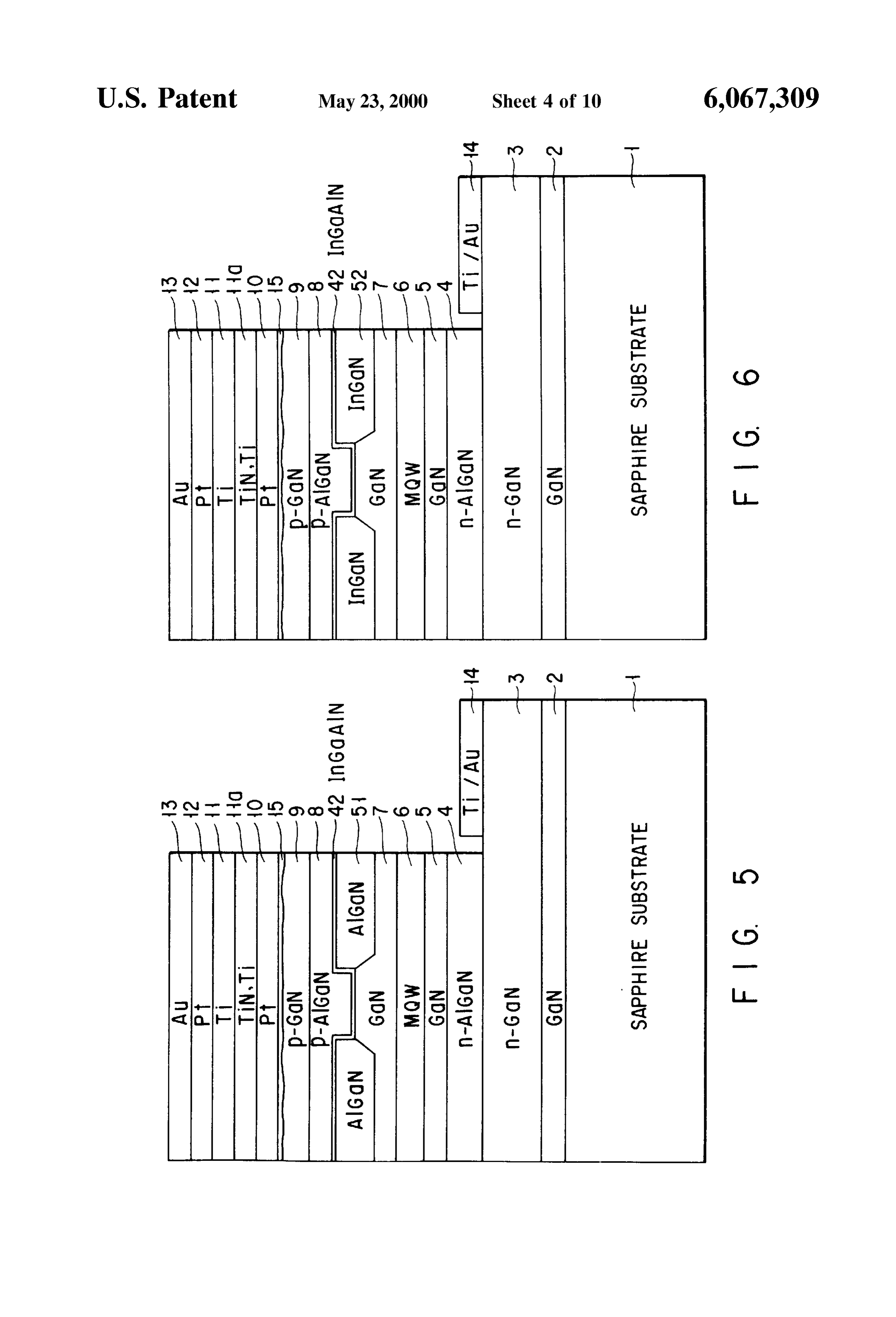
Moreover, in the case of an inner Stripe Structure, accord BRIEF DESCRIPTION OF THE SEVERAL ing to the present invention, there is provided a compound VIEWS OF THE DRAWING Semiconductor light-emitting device of gallium nitride Series The accompanying drawings, which are incorporated in having a compound Semiconductor of gallium nitride Series 60 and constitute a part of the Specification, illustrate presently (Ga, In, Al-N: X1+y1+Z1=1,0sX1, y1, Z1s 1), the com preferred embodiments of the invention, and together with pound Semiconductor light-emitting device comprising: the general description given above and the detailed descrip a Substrate; tion of the preferred embodiments given below, servo to a Semiconductor layer formed on the Substrate; explain the principles of the invention. an n-type clad layer formed on the Semiconductor layer; 65 FIG. 1 is a croSS-Sectional view showing the Schematic an n-type waveguide layer formed on the n-type clad Structure of a blue Semiconductor laser according to a first layer; embodiment of the present invention;
Page 14
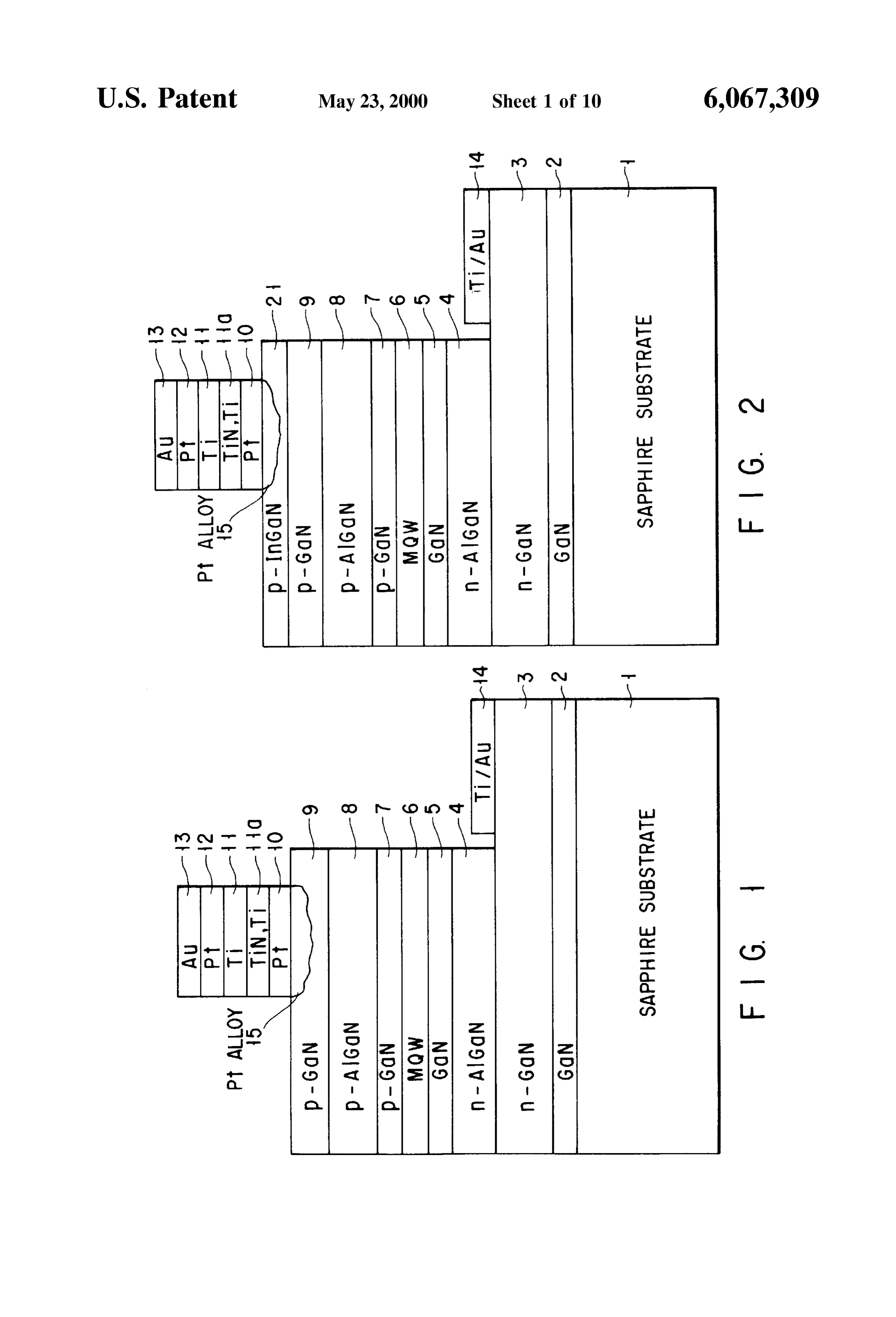
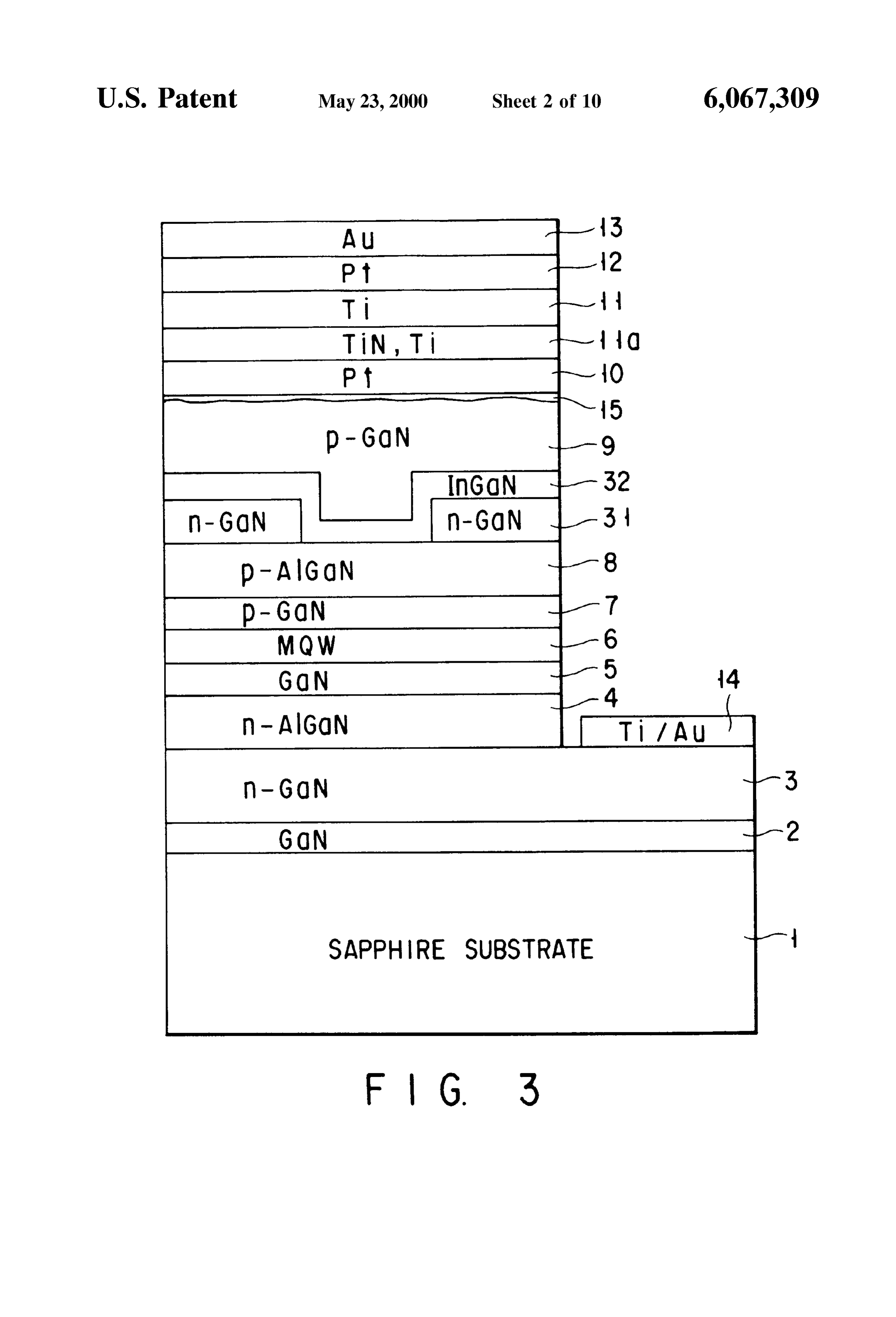
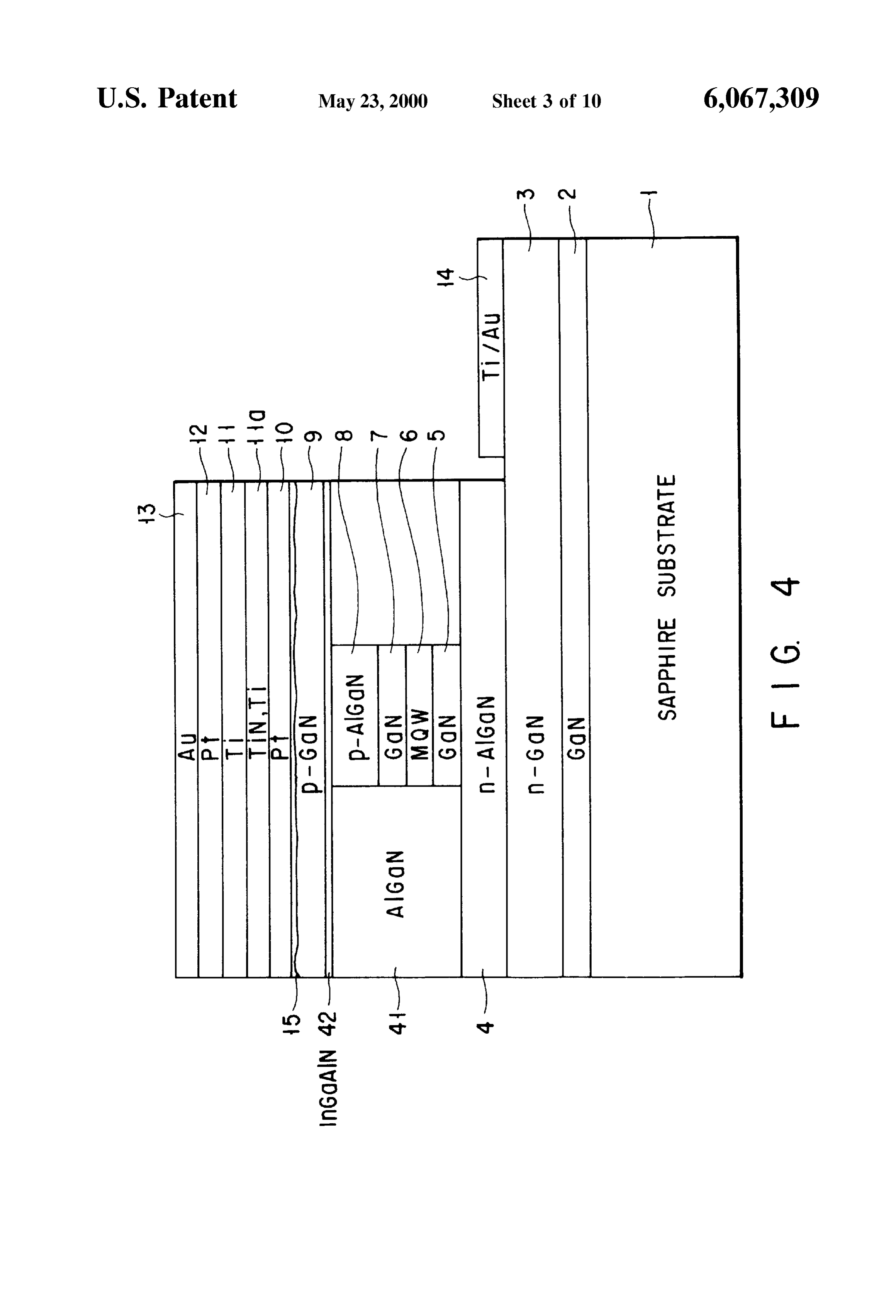
S 6
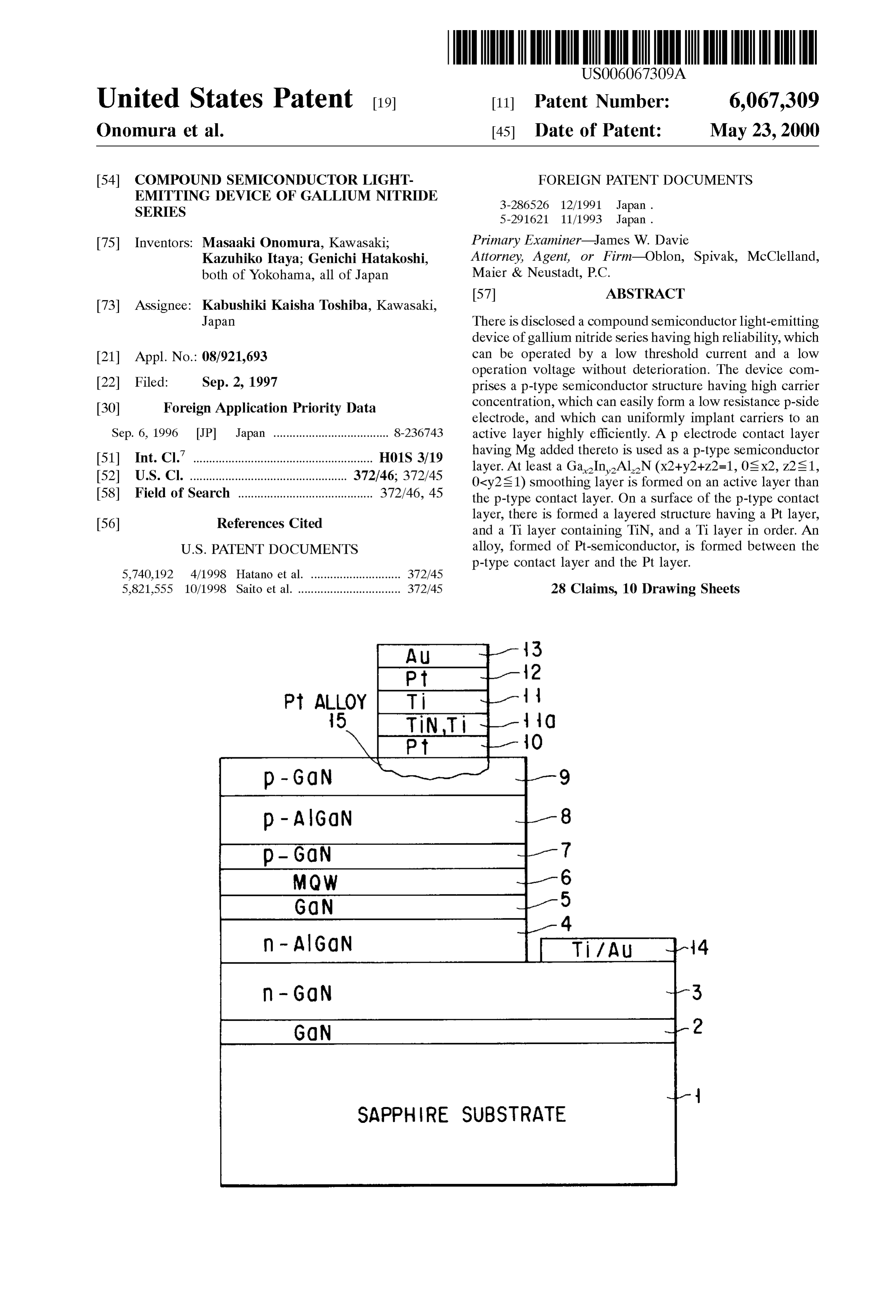
FIG. 2 is a croSS-Sectional view showing the Schematic portion reaching the n-type GaN contact layer 3 by dry Structure of a blue Semiconductor laser according to a etching. Thereby, on the exposed n-type GaN contact layer Second embodiment of the present invention; 3, an n-side electrode 14 is formed. FIG. 3 is a croSS-Sectional view showing the Schematic The active layer 6 is formed of InGaosN multi Structure of a blue Semiconductor laser according to a third quantum Wells (undope, 2.5 nm) and an Inoos Gaolos N embodiment of the present invention; barrier wall layers (undope, 5 nm), which are alternatively FIG. 4 is a croSS-Sectional view showing the Schematic layered on each other to make 10 layers in all. Also, the impurity in p-type GaN waveguide layer, p-type AlGaN clad
Structure of a blue Semiconductor laser according to a fourth layer and p-type GaN layer, are not limited to Mg, but may embodiment of the present invention; be any p-type impurity, like Zn. FIG. 5 is a cross-sectional view showing the schematic Next, the following will explain the manufacturing Structure of a blue Semiconductor laser according to a fifth method of the blue Semiconductor laser and its function. embodiment of the present invention; In FIG. 1, each of GaN buffer layer 2 to p-type GaN FIG. 6 is a croSS-Sectional view showing the Schematic contact layer 9 on the Sapphire substrate 1 is formed by one structure of a modification of the embodiment; 15
MOCVD.
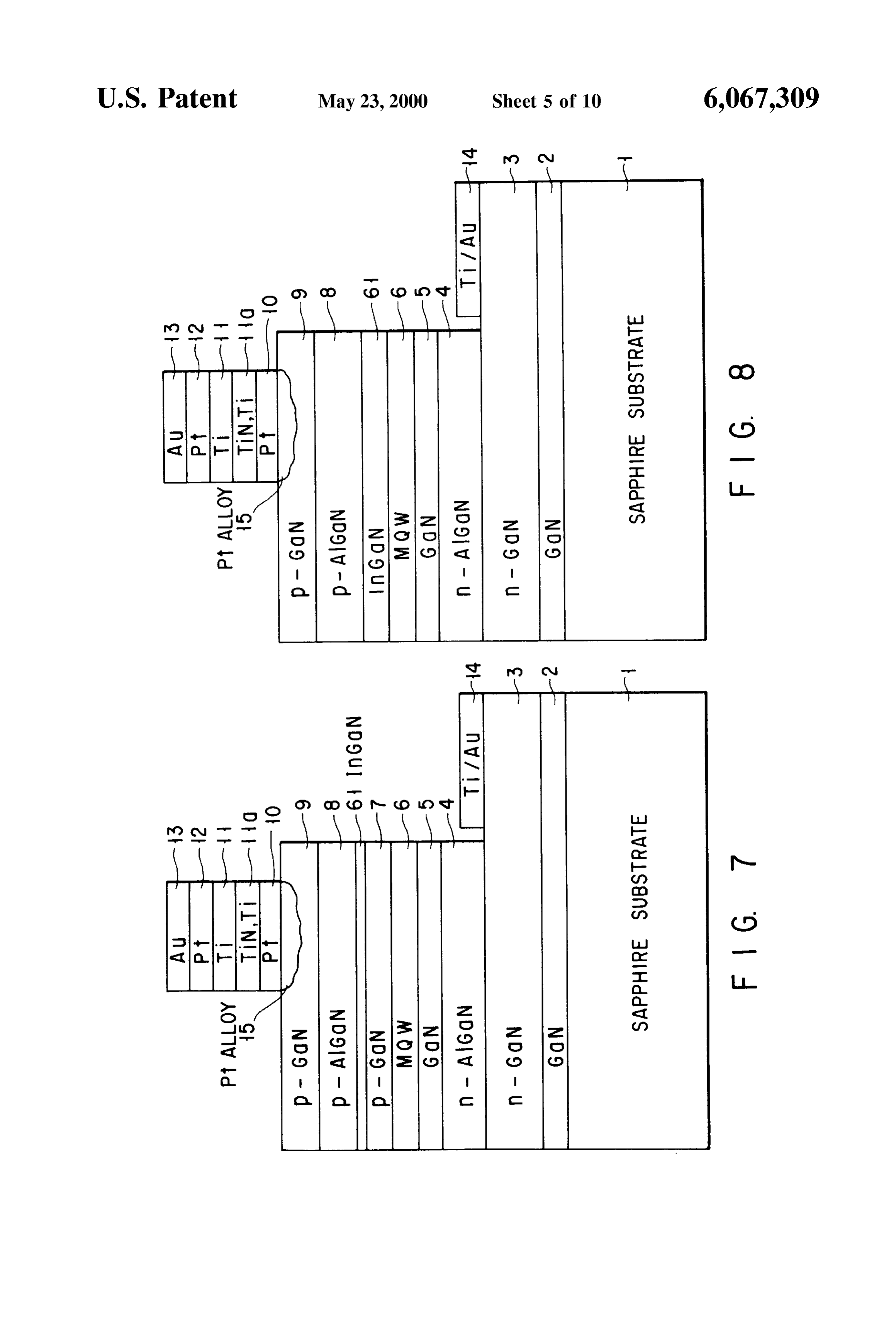
FIG. 7 is a cross-sectional view showing the schematic In the blue semiconductor laser, a GainAIN Smoothing Structure of a blue Semiconductor laser according to a sixth layer containing In is used as InGaN quantum well active embodiment of the present invention; layer 6, and semiconductors 7 and 9 of a nitride gallium FIG. 8 is a cross-sectional view showing the schematic series to which Mg is added are formed thereon. Due to this, structure of a modification of the embodiment; the GanAIN Smoothing layer restrains the fine porous FIG. 9 is a cross-sectional view showing the schematic defects propagated from the Substrate 1 and crystal defects Structure of a blue Semiconductor laser according to a Such as a crack and a transition. As a result, Smooth p-type Seventh embodiment of the present invention; Semiconductor layers can be obtained on the p-side electrode Side.
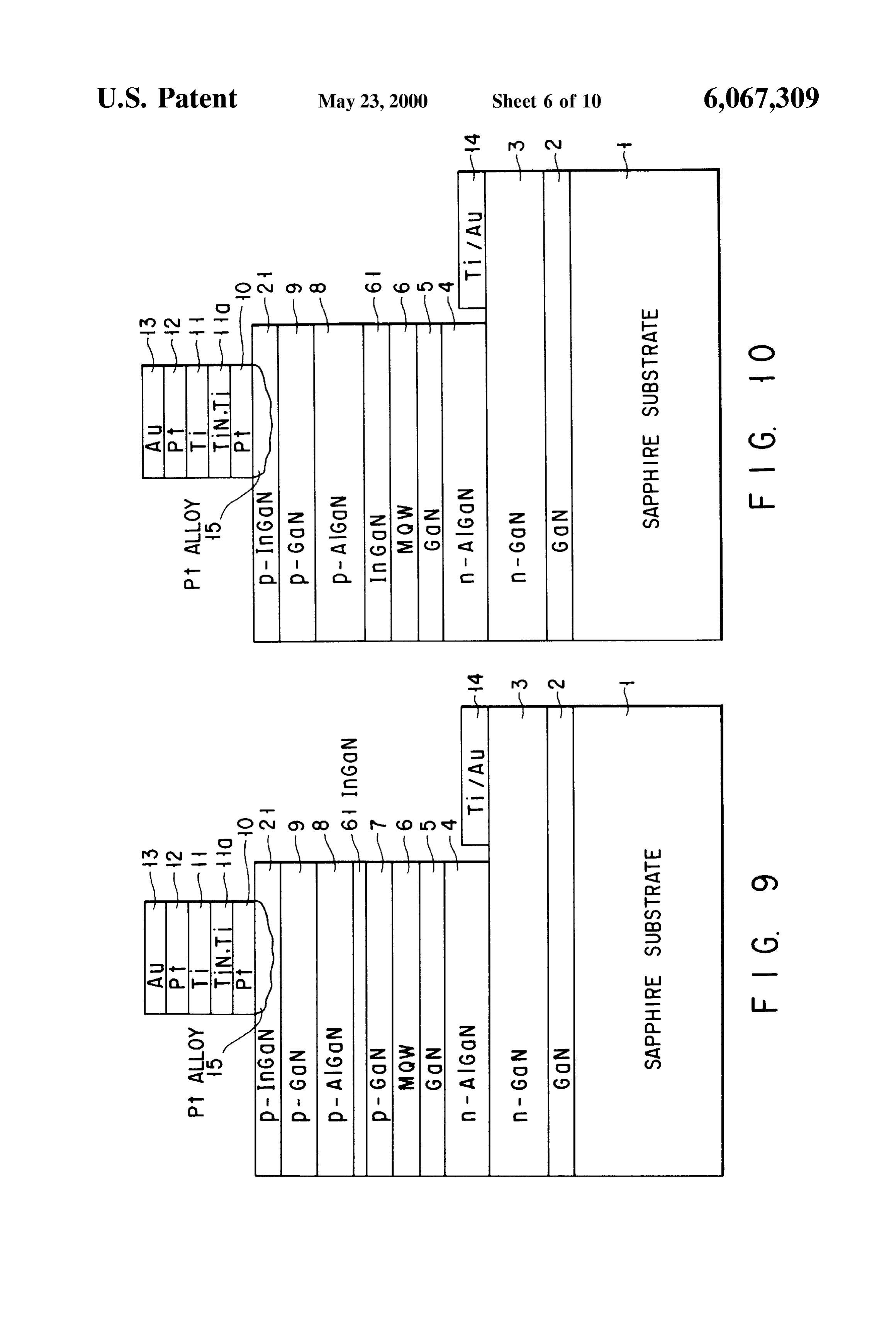
FIG. 10 is a cross-sectional view showing the schematic According to the experiment made by the inventors of the structure of a modification of the embodiment; 25 present invention, even if the GanAIN Smoothing layer is
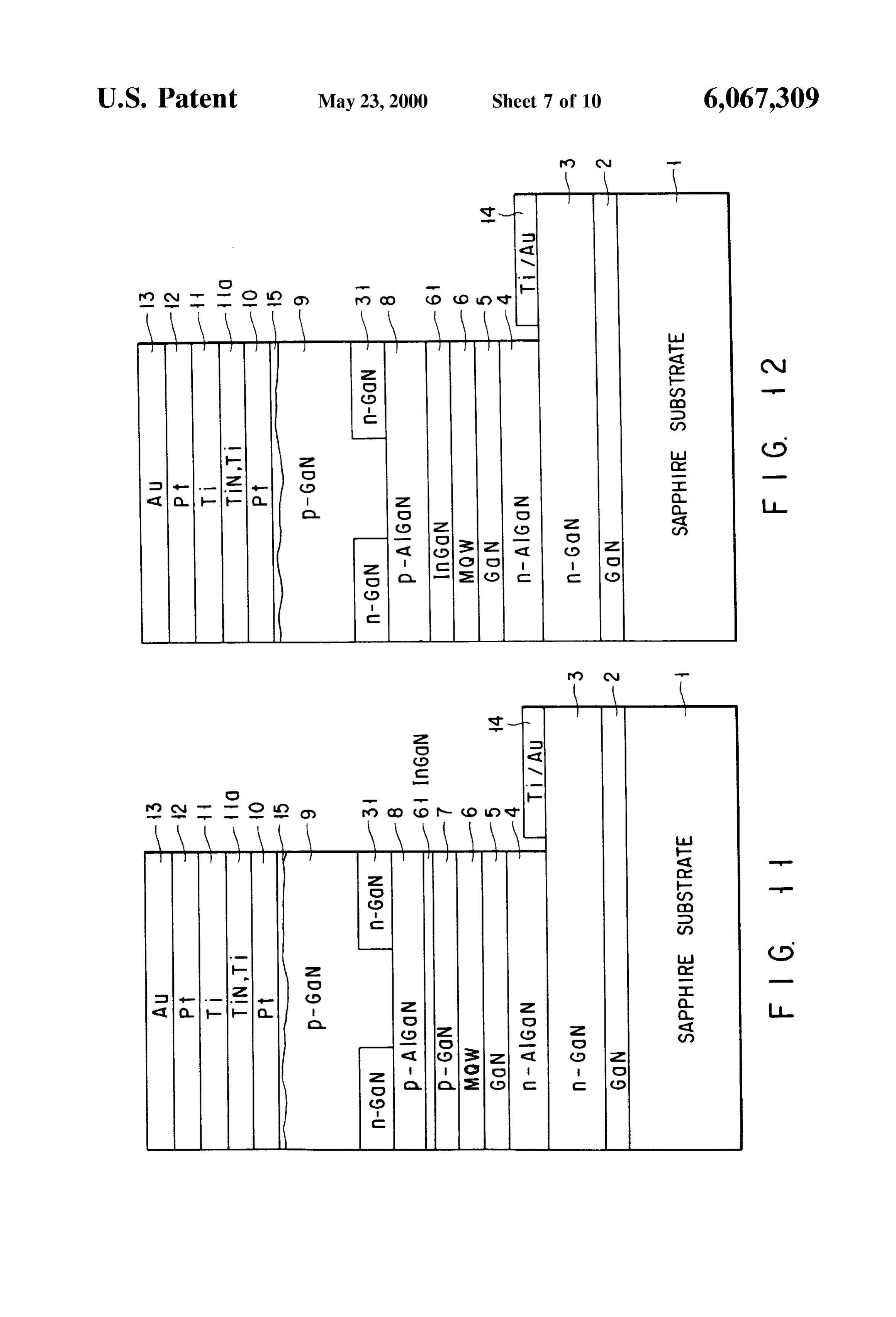
FIG. 11 is a croSS-Sectional view showing the Schematic not formed, the plurality of porous detects can be buried in Structure of a blue Semiconductor laser according to an the surface of the p-type GaN contact layer 9 when the eighth embodiment of the present invention; thickness of the p-type GaN contact layer 9 is 0.6 um and FIG. 12 is a cross-sectional view showing the Schematic more. In other words, in addition to the formation of the structure of a modification of the embodiment; GainAIN Smoothing layer, the thickness of the p-type GaN FIG. 13 is a cross-sectional view showing the schematic contact layer 9 is set to 0.6 um or more. Thereby, the quality Structure of a blue Semiconductor laser according to a ninth of the p-type Semiconductor layer can be Surely improved. embodiment of the present invention; Next, Pt (5 nm)/Ti (30 nm)/Pt (10 nm)/Au (1 lum) layers FIG. 14 is a cross-sectional view showing the Schematic 35 are Sequentially layered on a 10-width um area of the Surface structure of a modification of the embodiment; of the p-type GaN contact layer 9.
FIG. 15 is a cross-sectional view showing the schematic Then, when thermal treatment is provided to the entire Structure of a blue Semiconductor laser according to a tenth substrate under a nitrogenous atmosphere at 350° C., Pt is embodiment of the present invention; and diffused down to a depth, which is three times deeper than FIG. 16 is a cross-sectional view showing the Schematic 40 the thickness of the layered film at its maximum. Then, Pt is structure of a modification of the embodiment. solid phase reacted with Ga of p-type GaN contact layer 9, DETAILED DESCRIPTION OF THE so that an alloy layer 15 of Pt-semiconductor is formed. At INVENTION the same time, Ti is solid phase reacted with N diffusing upward from the p-type GaN contact layer 9. As a result, Ti
Embodiments of the present invention will now be 45 and N are stably combined with each other, the Tilayer 11a described with reference to the accompanying drawings. containing TiN is formed at a boundary Surface between the (First embodiment) Tilayer and the Pt layer. By this heat treatment, Pt works as FIG. 1 is a croSS-Sectional view showing the Schematic a catalyst, and hydrogen and carbon elements, which prevent Structure of a blue Semiconductor laser according to a first the activation of Mg (p-type dopant) as an acceptor, or an embodiment of the present invention. The blue semiconduc 50 oxygen element, which is combined with the Surface of the tor laser has a multi-layered structure having a GaN buffer contact layer 9 by air exposure before forming the electrode, layer 2, an n-type GaN contact layer (Sidope, 5x10" cm, are removed from the film. As a result, acceptor concentra 4 um)3, an n-type AloGaosN clad layer (Sidope, 5x10'7 tion is increased, and an activation ratio of Mg becomes cm, 0.3 um) 4, a GaN waveguide layer (undope, 0.1 um) Substantially 100% (the hydrogen, carbon, and oxygen ele 5, an active layer 6, a p-type GaN waveguide layer (Mg 55 ments are distributed in the multi-layered Structure having dope, 0.3 um) 7, a p-type AloGaosN clad layer (Mg dope, the respective Semiconductor layers at Substantially fixed 5x10'7 cm, 0.3 um)8, and a p-type GaN contact layer (Mg concentration before the above thermal treatment by various dope, 1x10" cm, 1 um) 9 sequentially formed on a reasons at a growth time).
sapphire substrate 1 by MOCVD. Moreover, on the boundary surface between the Ti layer On the p-type GaN contact layer 9, there are sequentially 60 11a containing TiN and the Pt layer 10, concentration of layered a Pt layer 10 having a thickness of 10 nm, a Tilayer each of carbon and oxygen elements is higher than that in the 11a containing TiN treated by heat (to be described later), a p-type GaN contact layer 9. In other words, in the process in Tilayer 11 having a thickness of 30 nm, a Pt layer 12 having which the carbon and oxygen of the Semiconductor layer are a thickness of 10 nm, and an Au electrode pad 13 having a removed outside by the catalyst of Pt, they are stopped by thickness of 1 tim, thereby forming a p-type electrode. 65 the Ti layer 11a containing TiN.
A part of the uppermost Surface of the Au electrode pad Furthermore, on the boundary Surface between the Pt 13 and the p-type GaN contact layer 9 are removed up to a layer 12 and the Au layer 13, hydrogen concentration is
Page 15
higher than that in the p-type GaN contact layer 9. In other Therefore, there can be realized a compound Semicon words, in the proceSS in which the carbon and oxygen of the ductor Structure of p-type gallium nitrite Series with a high Semiconductor layer are removed outside by the catalyst of carrier concentration, which can easily form a low resistance Pt, they are stopped by the Au layer 13. p-side electrode, and which can implant carriers to an active Next, a mesa Shape containing a p-side electrode is layer uniformly and efficiently. Then, the Voltage drop formed to form the n-side electrode 14. The n-side electrode generated by the electrode contract can be restrained, and no 14, which is made of Ti/Au, is formed on the n-type GaN deterioration occurs under conditions of a low threshold contact layer 3 appearing at a lower portion of the mesa current and a low operation Voltage without deterioration, So form. In this case, the p-Side electrode may be formed after that excellent reliability can be brought about. forming the n-side electrode 14. Moreover, the Sapphire (Second embodiment)
Substrate 1 is mirror polished up to 50 lum, and cleaved in a Next, the blue semiconductor laser of the Second embodi Vertical direction against the longitudinal direction of the ment will be explained. FIG. 2 is a cross sectional view p-side electrode. Thereby, a laser chip having a length of 1 showing the Schematic Structure of the blue Semiconductor mm is formed. laser. In FIG. 2, the same reference numerals as FIG. 1 are The above-explained blue Semiconductor laser was con 15 added to the portions common to FIG. 1, and the Specific tinuously generated at room temperature at the threshold explanation will be omitted. Then, only the portions differ current of 80 mA. In this case, the wavelength was 420 nm, ent from FIG. 1 will be described.
the operation Voltage was 7V, and a device life time was The semiconductor laser of this embodiment is to further 5000 hours under conditions of 50° C. and 30 mW drive. In improve contact resistance as compared with the first the case of this laser, the Substantial contact area between the embodiment. More specifically, FIG. 2 shows the structure Pt layer 10 and the p-type GaN contact layer 9 was in which a p-type Inc. GaN contact layer 21 is inserted increased. Due to this, resistance was reduced to 1x10
G2cm. Also, an Mg activation ratio of the p-type GaN between the p-type GaN layer 9 and the Pt electrode 10. contact layer 9 was improved to substantially 100%. As a 25 tor layer (Mg Ino,
The p-type GaoN contact layer 21 is a Semiconduc
result, high carrier concentration was obtained, and the carriers were uniformly implanted to the active layer 6 Excepting for the formation of the p-type Ino, GaoloN through the P-type AlGaN clad layer 8. contact layer 21, this blue Semiconductor laser is manufac Moreover, in the blue semiconductor laser in which tured by the same way as the first embodiment. two-step dope is provided, the characteristic was further The above-explained blue Semiconductor laser was con improved. In this case, the two-step dope means that the tinuously generated at room temperature at the threshold amount of addition of Mg to the P-type GaN contact layer current of 75 mA. In this case, the wavelength was 420 nm, of the above-explained first embodiment is doubled in the the operation Voltage was 6V, and a device life time was range from the Surface to 0.2 um and is set to /2 in the 5000 hours under conditions of 50° C. and 30 mW drive. residual range of 0.8 um. More specifically, in this structured 35 According to this laser, in the contact layer 21 contacting Pt Semiconductor laser, the operation Voltage was further layer 10, Since a bandgap is narrower than the p-type GaN reduced to 6.5V as compared with the first embodiment. By layer 9, a Schottky barrier was reduced. Therefore, electrode forming the p-type contact layer in the two-step dope contact resistance was reduced to 7x10 S2cm together manner, there were obtained an advantage in which elec with the Substantial contact area increasing effect. In trode contact resistance on the Surface was reduced and an addition, the Mg activation ratio of the contact layer 21 was advantage in which resistance of the lower portion of the 40 improved to substantially 100%. As a result, high carrier contact layer was increased to control the leak current to the concentration was obtained, and the carriers were uniformly horizontal direction. implanted to the active layer 6 through the p-type AlGaN According to the above-mentioned first embodiment, the clad layer 8.
Semiconductor layer of nitride gallium Series to which Mg is 45 Thus, according to the Second embodiment, the contact added is formed on the GanAIN Smoothing layer containing layer 21 whose bandgap is narrower than the p-type GaN at least In, thereby reducing crystal defects Such as porous layer 9 is inserted between the p-type GaN layer 9 and the micro detects. Pt electrode 10. As a result, in addition to the advantage Also, the Pt layer 10 is formed on the p-type GaN contact explained in the first embodiment, contact resistance with layer 9, and the Pt layer is slightly diffused to the p-type GaN 50 the p-side electrode can be further reduced, So that the contact layer 9. Thereby, the effective electrode contact area reduction of the operation Voltage can be improved. is increased. The Pt element works as reduction catalysts of (Third embodiment) the hydrogen element, the carbon element, and the oxygen Next, the blue semiconductor laser of the third embodi element, which exist in the p-type Semiconductor layer by ment will be explained. FIG. 3 is a cross sectional view various reasons. Then, these impurity elements are removed 55 showing the Schematic Structure of the blue Semiconductor from the p-type Semiconductor layer. As a result, the acti laser. In FIG. 3, the same reference numerals as FIG. 1 are Vation ratio of Mg can be improved, and effective acceptor added to the portions common to FIG. 1, and the Specific concentration can be increased. explanation will be omitted. Then, only the portions differ Moreover, the Tilayer 11 is formed on the Pt layer 10, and ent from FIG. 1 will be described.
the Tilayer reacts with the N element of the semiconductor 60 Unlike the first embodiment, the semiconductor laser of layer of nitride gallium Series, So that the extremely stable this embodiment has an inner Stripe Structure. Specifically, TiN is formed. As a result, the second Pt layer 12, serving as shown in FIG. 3, in the inner Stripe Structure, there are as an upper electrode metal and the Au layer 13 can be formed a plurality of n-type GaN current block layers 31 prevented from being diffused downward. (1x10" cm, 0.5 um), which are selectively formed on By the respective advantages of these GainAIN Smooth 65 p-type AloGaosN clad layer 8, and an Ino, GaooN Smooth ing layer, Pt layer 10, and Ti layer 11, the quality of the ing layer 32 with a thickness of 0.1 um, which is formed on crystal can be improved. the clad layer 8 and each current block layer 31.
Page 16
Similarly, On the Ino, GaooN Smoothing layer 32, the showing the Schematic Structure of the blue Semiconductor p-type GaN contact layer 9 is formed. laser. In FIG. 5, the same reference numerals as FIG. 1 are This blue semiconductor laser is manufactured by the added to the portions common to FIG. 1, and the Specific Same way as the first embodiment, except that the number of explanation will be omitted. Then, only the portions differ times of growths by MOCVD is three due to the inner stripe ent from FIG. 1 will be described. Structure.
Unlike the first embodiment, the semiconductor laser of
The above-explained blue Semiconductor laser was con this embodiment has an inner Stripe Structure. Specifically, tinuously generated at room temperature at the threshold as shown in FIG. 5, a junction between the GaN waveguide current of 70 mA. In this case, the wavelength was 420 nm, layer 7 and the p-type AlosGaoN clad layer 8 is formed the operation Voltage was 6.5V, and a device life time was through the InGaAlN smoothing layer 42. Then, the inner 5000 hours under conditions of 50° C. and 30 mW drive. Stripe Structure is formed of an undope Alo, Gaolo N block According to this laser, in addition to the advantage layer 51.
explained in the first embodiment, Since the inner Stripe The GaN waveguide layer 7, which is formed on the Structure was formed, the area of the p-Side electrode was active layer 6, is an undope Semiconductor layer having a increased, and p-side electrode contact resistance was 15 reduced to 5x10 G2cm. In other words, the low voltage mesa lum. A
Shape having a width of 10 tim, and a thickness of 0.2 mesa lower portion of the GaN waveguide layer 7 has operation was further improved by the inner Stripe Structure. a thickness of 0.1 tim, and the undope Alo, Gaolo N block Thus, according to the third embodiment, contact resis layer 51 is formed thereon.
tance can be further reduced in addition to the advantage The p-type AloGao N clad layer 8 has a window having explained in the first embodiment. a width of 10 lim. The p-type AlosGaN clad layer 8 is Even if the p-type GaN contact layer 9 is formed just on the Inc. GaN Smoothing layer 32, the Smoothing layer 32 formed on the mesa upper portion of the GaN waveguide prevents the propagation of porous micro detects. Therefore, layer the 7 and the undope Alo, Gaolo N block layer 51 through
InGaAlN Smoothing layer 42 such that the window is the quality of the crystal can be improved.
25 opposite to the mesa upper portion of the GaN waveguide
(Fourth embodiment) layer 7. The p-type AlosGaN clad layer 8 is a layer of Mg Next, the blue semiconductor laser of the fourth embodi dope, 5x107 cm, (window) thickness of 0.3 um). ment will be explained. FIG. 4 is a cross sectional view This blue semiconductor laser is manufactured by the showing the Schematic Structure of the blue Semiconductor Same way as the first embodiment, except that the number of laser. In FIG. 4, the same reference numerals as FIG. 1 are times of growths by MOCVD is three due to the inner stripe added to the portions common to FIG. 1, and the Specific Structure.
explanation will be omitted. Then, only the portions differ ent from FIG. 1 will be described. The above-explained blue Semiconductor laser was con Unlike the first embodiment, the semiconductor laser of current of generated tinuously at room temperature at the threshold this embodiment has a buried inner Stripe Structure. 35 the operation Voltagethis 60 mA. In case, the wavelength was 420 nm,
Specifically, as shown in FIG. 4, the GaN waveguide layer 5000 hours under conditions5V, was and a device life time was of 50° C. and 30 mW drive. In 5 to the p-type AloGaosN clad layer 8 are formed to have the case of this laser, the same advantage as the fourth the mesa Structure having a width of 10 um. Then, an undope embodiment was obtained.
Alo. GaN block layer 41 is formed on both ends of the mesa structure. Moreover, an InCaAlN Smoothing layer 42 40 (Modification) is formed among the Alo, Gaolo N block layer 41, the p-type As shown in FIG. 6, the InGaN block layer 52 may be AloGaosN clad layer 8, and the p-type GaN contact layer used in place of the AlGaN block layer 51. The modification 9. using the InGaN layer 52 can control a transverse mode This blue semiconductor laser is manufactured by the well.
Same way as the first embodiment, except that the number of 45 (Sixth embodiment) times of growths by MOCVD is three due to the buried inner Next, the blue semiconductor laser of the sixth embodi Stripe Structure. ment will be explained. FIG. 7 is a cross sectional view The above-explained blue Semiconductor laser was con showing the Schematic Structure of the blue Semiconductor tinuously generated at room temperature at the threshold laser. In FIG. 7, the same reference numerals as FIG. 1 are current of 60 mA. In this case, the wavelength was 420 nm, 50 added to the portions common to FIG. 1, and the Specific the operation Voltage was 5V, and a device life time was explanation will be omitted. Then, only the portions differ 5000 hours under conditions of 50° C. and 30 mW drive. ent from FIG. 1 will be described. According to this laser, in addition to the advantage Unlike the first embodiment in which the active layer explained in the first embodiment, Since the buried inner (MOW) 6 also serves as a GainAIN Smoothing layer con Stripe Structure was formed, the areas of the p-Side elec 55 taining In, an InCaN Smoothing layer 61 of GainAIN series trodes were increased, and p-Side electrode contact resis material containing In is formed between the p-type AlGaN tance was reduced to 5x10 G2cm. In other words, by the clad layer 8 and the p-type GaN waveguide layer 7. reduction of the gain level of oscillation threshold due to the The InGaN Smoothing layer 61 can be formed in a range thin film quantum well active layer whose thickness is leSS in which In composition is over, e.g., 0 and 0.3 or less. If the than a critical film thickness and the buried inner Stripe 60 In composition is higher than the In composition of the Structure, the low Voltage operation was further improved. quantum well layer of the active layer 6, the thickness of the Thus, according to the fourth embodiment, the inner Stripe InGaN Smoothing layer 61 is formed to be thinner than the Structure can be formed in addition to the advantage thickness of the quantum well layer. For example, in the first explained in the first embodiment. embodiment, the InGaosN well layer having a thickness (Fifth embodiment) 65 of 2.5 nm is used. In accordance with this condition, the Next, the blue semiconductor laser of the fifth embodi InGaN Smoothing layer 61 of the sixth embodiment uses ment will be explained. FIG. 5 is a cross sectional view In Gao,N layer having a thickness of 1.5 nm.
Page 17
Thus, in the case having the high In composition and the The composition of the InGaN Smoothing layer 61 and the thick film thickness, the Smoothing layer functions as Super film thickness are the same as explained in the Sixth embodi Saturated absorption layer. Due to this, the Structure of this ment. The same advantage as the third and Sixth can be embodiment can operate as a laser with low noise, which is obtained by the above-mentioned structure. Particularly, in necessary to, e.g., an optical disk System. the eighth embodiment having the block layer 31, by the If the In composition is lower than the In composition of increase in the effective refractive index of the active layer the quantum well layer of the active layer 6, the thickness of 6, an equivalent refractive index of the active layer 6 is the InGaN Smoothing layer 61 is formed to be thicker than increased, the difference between the active layer 6 and the the thickness of the quantum well layer. For example, in the block layer 31 in the refractive indeX is enlarged. As a result, first embodiment, the InGaosN well layer having a thick the fundamental transverse mode is Stabilized, and an astig neSS of 2.5 nm is used. In accordance with this condition, the matic difference is decreased, So that the laser, which is Smoothing layer 61 of this embodiment uses a layer of Suitable for the optical System, can be realized. In GaooN having a thickness of 0.1 um. The Ino, GaooN (Ninth embodiment) smoothing layer 61 may be replaced with the p-type GaN Next, the blue semiconductor laser of the ninth embodi waveguide layer 7 as shown in FIG. 8. 15 ment will be explained. FIG. 13 is a cross sectional view
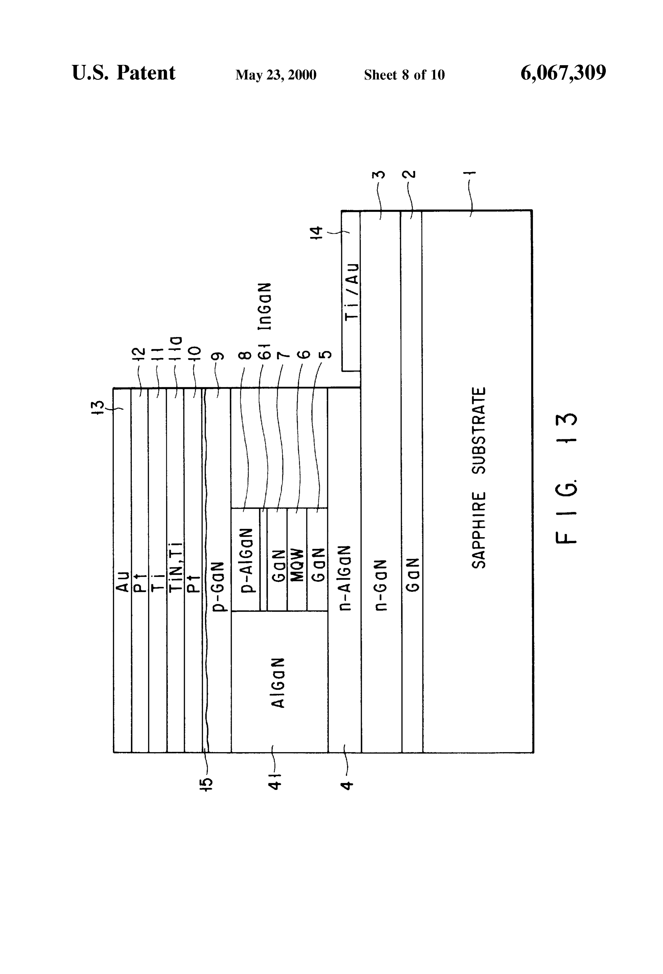
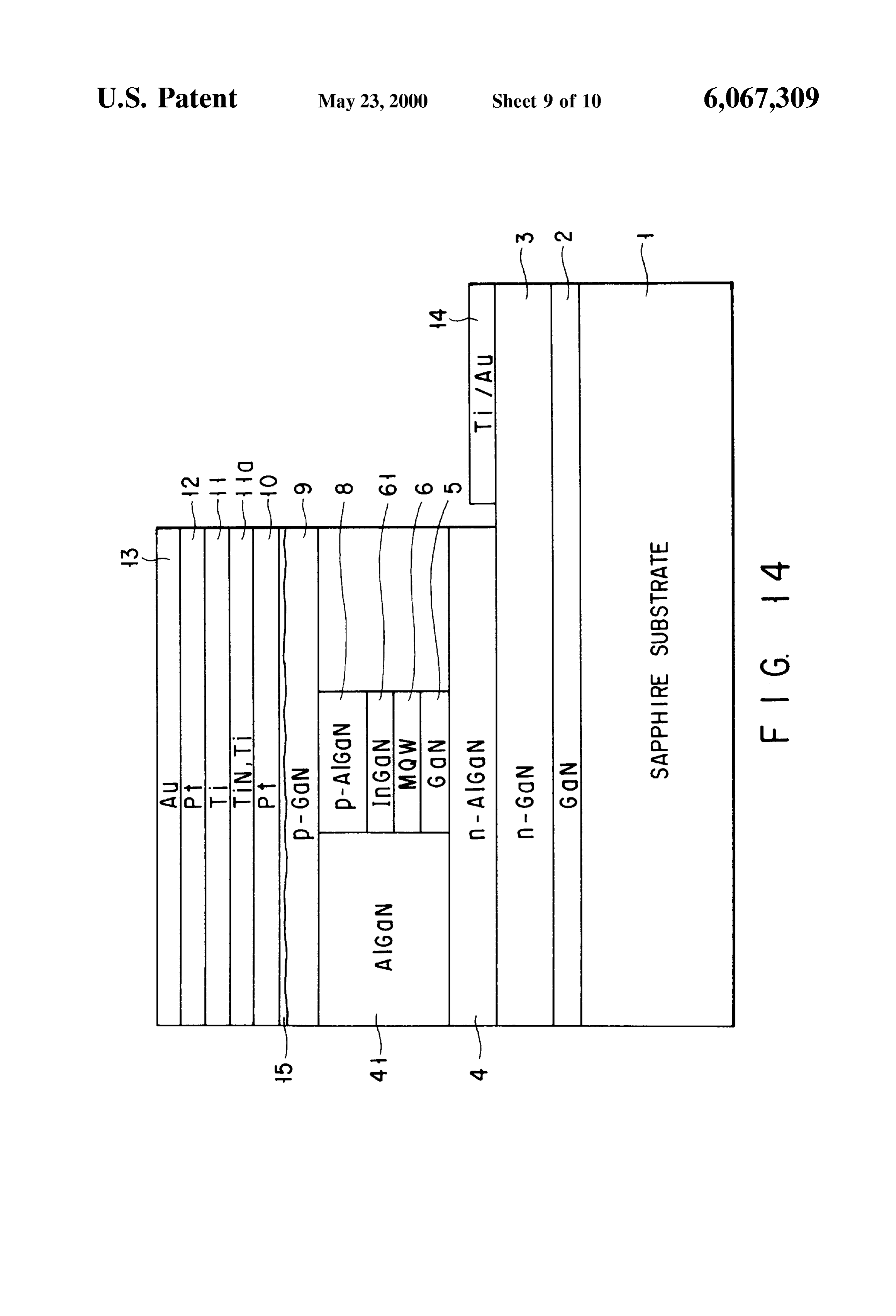
Thus, in the case having the low In composition and a showing the Schematic Structure of the blue Semiconductor high film thickness, the effective refractive index of the laser, and FIG. 14 is a croSS-Sectional view showing the active layer 6 is increased, so that a light guiding (or modification. In these figures, the Same reference numerals confining) characteristic can be improved. In accordance as FIG. 4 are added to the portions common to FIG. 4, and with the increase in the light guiding characteristic, the the specific explanation will be omitted. Then, only the p-type AlGaN clad layer 8 can function even if the film portions different from FIG. 4 will be described. thickneSS is reduced. As compared with the fourth embodiment having the In the case where the In composition is low, the film buried inner stripe structure, as shown in FIG. 13, thickneSS is increased, and p-type carrier concentration is Set 25 Ino. GaN Smoothing layer 42 is omitted. Then, the InGaN to 1x10 cm or more. Thereby, the overflow of the Smoothing layer 61 of GanAIN Series material containing. In electrons can be prevented, and the laser can be generated by is formed between the p-type AlGaN clad layer 8 and the the low threshold value. p-type GaN waveguide layer 7, similar to the sixth embodi (Seventh embodiment) ment. Or, as shown in FIG. 14, the InGaN Smoothing layer Next, the blue semiconductor laser of the seventh embodi 61 is formed in place of the p-type GaN waveguide layer 7. ment will be explained. FIG. 9 is a cross sectional view The composition of the InGaN Smoothing layer 61 and the showing the Schematic Structure of the blue Semiconductor film thickness are the same as explained in the Sixth embodi laser, and FIG. 10 is a cross-sectional view showing the ment. The same advantage as the fourth and Sixth can be modification. In these figures, the Same reference numerals obtained by the above-mentioned structure. as FIG. 2 are added to the portions common to FIG. 2, and 35 (Tenth embodiment) the specific explanation will be omitted. Then, only the Next, the blue semiconductor laser of the tenth embodi portions different from FIG. 2 will be described. ment will be explained. FIG. 15 is a cross sectional view AS compared with the Second embodiment having the showing the Schematic Structure of the blue Semiconductor p-type Ino, GaooN contact layer 21, as shown in FIG. 9, the laser, and FIG. 16 is a croSS-Sectional view showing the InGaN Smoothing layer 61 of GainAIN series material 40 modification. In these figures, the Same reference numerals containing In is formed between the p-type AlGaN clad as FIG. 5 are added to the portions common to FIG. 5, and layer 8 and the p-type GaN waveguide layer 7, similar to the the specific explanation will be omitted. Then, only the sixth embodiment. Or, as shown in FIG. 10, the InGaN portions different from FIG. 5 will be described. smoothing layer 61 is formed in place of the p-type GaN As compared with the fifth embodiment having the inner waveguide layer 7. 45
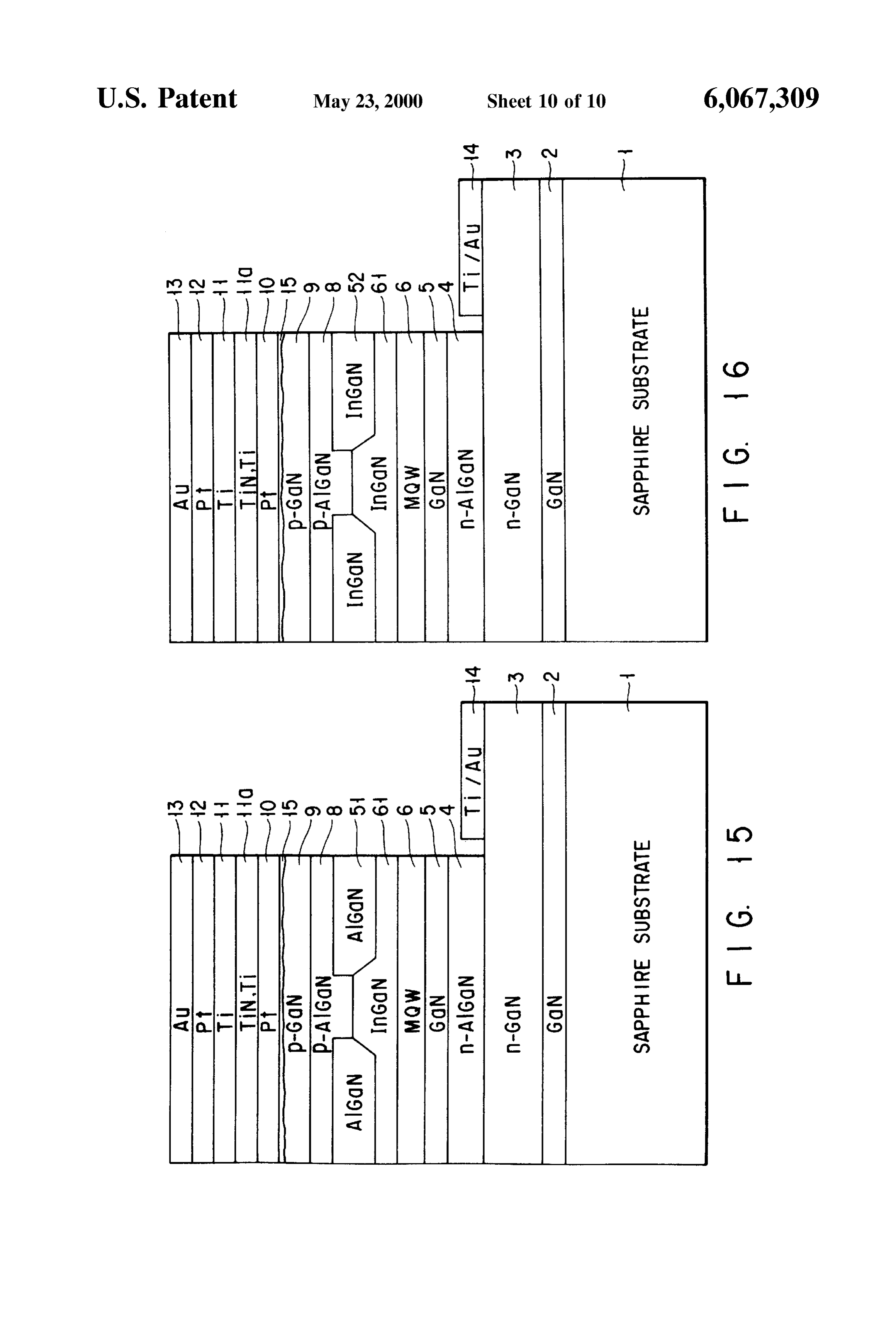
Stripe Structure, as shown in FIG. 15, Ino. GaN Smoothing
The composition of the InGaN Smoothing layer 61 and the layer 42 is omitted. Then, the InGaN Smoothing layer 61 of film thickness are the same as explained in the Sixth embodi GanAIN Series material containing In is formed in place of ment. The same advantage as the Second and Sixth can be the p-type GaN waveguide layer 7, similar to the sixth obtained by the above-mentioned structure. embodiment.
(Eighth embodiment) The composition of the InGaN Smoothing layer 61 and the Next, the blue semiconductor laser of the eighth embodi film thickness are the same as explained in the Sixth embodi ment will be explained. FIG. 11 is a cross sectional view ment. The same advantage as the fifth and Sixth can be showing the Schematic Structure of the blue Semiconductor obtained by the above-mentioned structure. Particularly, in laser, and FIG. 12 is a cross-sectional view showing the 55 the tenth embodiment having the block layer 51, similar to modification. In these figures, the Same reference numerals the third embodiment, the fundamental transverse mode is as FIG. 3 are added to the portions common to FIG. 3, and Stabilized, and an astigmatic difference is decreased, So that the specific explanation will be omitted. Then, only the the laser, which is Suitable for the optical System, can be portions different from FIG. 3 will be described. realized. As shown in FIG. 16, according to this AS compared with the third embodiment having the inner embodiment, it is needless to say that the InGaN block layer
Stripe structure, as shown in FIG. 11, Inc. GaN Smoothing 52 can be used in place of the AlGaN block layer 51. layer 32 is omitted. Then, the InGaN smoothing layer 61 of (Other embodiments)
GainAIN series material containing. In is formed between (P-side electrode structure) the p-type AlGaN clad layer 8 and the p-type GaN In the above first to tenth embodiments, Pt/Ti/Pt/Au were waveguide layer 7, Similar to the Sixth embodiment. Or, as 65 vaporized to form the layered structure of Pt/Ti(N)/Ti/Pt/Au shown in FIG. 12, the InGaN Smoothing layer 61 is formed in forming the p-side electrode. The present invention is not in place of the p-type GaN waveguide layer 7. limited these embodiments. In place of Pt between Ti and
Page 18
Au, a plurality of conductive layerS or a single Nior Mo may Structured. Also, the present invention may be applied to the be formed. The reason is that Ni and Mo have dry etching electronic devices Such as a light receiving device, and a resistance as high as Pt and they are Suitable for a dry etching transistor other than the light-emitting device. process. There is a case in which the Structure having the Additional advantages and modifications will be readily plurality of conductive layerS is needed in the electrode occur to those skilled in the art. Therefore, the invention in wiring. The material of each conductive layer is prevented its broader aspect is not limited to the Specific details and from being diffused downward by Ti. Au or Al is preferably respective devices shown and described here in. used as a top portion of the p-side electrode. Au is Suitable Accordingly, various modifications may be made without for a wire assembly using an Au wire, and this can prevent departing from the Spirit or Scope of the general inventive the Surface of the p-side electrode from being oxidized. Al concept as defined by the appended claims and their equiva can be also used in the wire assembly. Also, a metal layer in lents.
contact with p-type GaN contact layer, is not limited to Pt, We claim:
but may be another metal layer e.g. Pd or Ni. In this case, a 1. A compound Semiconductor light-emitting device hav thickness of the metal layer is preferably thinned to 50 nm ing a compound semiconductor (Ga, In, Al-N: X1+y1+Z1= or less. 15 1,0s X1, y1, Z1s 1) comprising: (N-side electrode structure) an n-type Semiconductor layer having at least an n-type In the first to tenth embodiments, the n-side electrode was clad layer;
formed of Ti/Au. However, the present invention is not an active layer formed on Said n-type Semiconductor limited to the above-mentioned embodiments. The n-side layer;
electrode may be formed of Al/Ti/Au. If there is no process a p-type Semiconductor layer, formed on Said active layer, having a heat history of 400 C. or more after forming the having at least a p-type clad layer; n electrode, the structure of Al/Ti/Au has lower contact resistance. a Smoothing layer of Ga-In, Al-N (x2+y2+Z2=1,0sX2, (Relevant invention) Z2s 1, 0<y2s 1) formed in said active layer; 25 a p-type contact layer, formed on Said p-type Semicon
The following will explain the relevant invention to the ductor layer, having a p-type impurity added thereto, above-explained present invention. To Supply a current to a p-type Semiconductor of GaN Series, there is formed a a p-side electrode formed on Said p-type contact layer; p-type Semiconductor layer containing 1% or more of each and of palladium (Pd) or Pt and Ti. Thereby, the reduction of the an n-side electrode electrically connected with Said n-type operation Voltage and the control of the heating value are Semiconductor layer.
improved. Moreover, the diffusion due to the electrical 2. The compound Semiconductor light-emitting device conduction of the constituent elements is prevented, So that according to claim 1, wherein Said p-type contact layer reliability is improved. contains Mg as Said p-type impurity. For example, to Supply the current to the p-type Semi 35 3. A compound Semiconductor light-emitting device hav conductor layer of the compound Semiconductor device of ing a compound semiconductor (Ga, In, Al-N: X1+y1+z1= III-V group having a hexagonal crystal Structure, there is 1,0s X1, y1, Z1s 1) comprising:
formed a p-type Semiconductor layer containing 1% or more an n-type Semiconductor layer having at least an n-type of each of Pd or Pt and Ti. Thereby, Substantial electrode clad layer;
contact area is increased, and electrode resistance can be 40 an active layer formed on Said n-type Semiconductor reduced to about 10 S2cm. Moreover, the layer formed in layer;
the area, which is shallow from the Surface of the Semicon a p-type Semiconductor layer, formed on Said active layer, ductor of GaN series, contains the combination of Ti and N. having at least a p-type clad layer; AS a result, a stable diffusion prevention layer is formed, and the element diffusion occurred at the time of turning on 45 a Smoothing layer of Ga-In, 2Al-N (x2+y2+Z2=1,0sX2, electricity can be restrained, and the deterioration of the Z2s 1, 0<y2s 1) formed in said active layer; device can be prevented. a p-type contact layer, formed on Said p-type Semicon Also, the p-type Semiconductor layer is Structured to be a ductor layer, having a p-type impurity added thereto, semiconductor of Gain, Al-N (0s x, y, zs 1, and Z+y+Z=1). an alloy layer, made of Pt-Semiconductor, Selectively Thereby, electrode resistance to the p-type Semiconductor 50 formed on a Surface of Said p-type contact layer; layer, which contains 1% or more of each of Pd or Pt and Ti, a p-side electrode, containing a layered Structure made of can be reduced to 10 S2cm. Moreover, in the semicon a Pt layer formed on said alloy layer, a Ti layer ductor device having Pd or Pt (ranging 10 nm or less) containing TiN, thereon, and a Ti layer thereon, and formed on the Surface of the p-type Semiconductor layer of an n-side electrode electrically connected with Said n-type the compound Semiconductor device of III-V group having 55 Semiconductor layer.
a hexagonal crystal structure, Ti (ranging 50 nm or less) 4. The compound Semiconductor light-emitting device formed thereon, and an electrode metal for Supplying a according to claim 3, wherein an Aulayer is formed on Said current to the p-type Semiconductor layer formed thereon, Ti layer through a second Pt layer.
there can be formed a p-type Semiconductor layer having a 5. The compound Semiconductor light-emitting device thickness of 20 nm or leSS and containing 1% or more of 60 according to claim 3, wherein Said p-type contact layer each of Pd or Pt, which has chemically strong combination contains carbon, and carbon concentration of a boundary in the heating treatment of 300° C. or more, and Ti. between said Ti layer containing TiN, and said Pt layer is (Others) higher than carbon concentration of Said p-type contact The present invention and the relevant invention are not layer.
limited to the first to tenth embodiments. The composition 65 6. The compound Semiconductor light-emitting device and the thickness of the Semiconductor layer may be vari according to claim 3, wherein Said p-type contact layer ously changed, and the conductivity may be oppositely contains carbon and oxygen, and carbon concentration of a
Page 19
boundary between said Ti layer containing TiN and said Pt a p-type contact layer, formed on Said p-type Semicon layer is higher than carbon concentration of Said p-type ductor layer, having a p-type impurity added thereto, contact layer, and oxygen concentration of Said boundary is a p-side electrode formed on Said p-type contact layer; higher than oxygen concentration of Said p-type contact and layer. 5 an n-side electrode electrically connected with Said n-type 7. The compound Semiconductor light-emitting device Semiconductor layer, wherein Said n-type Semiconduc according to claim 3, wherein Said p-type contact layer tor layer, wherein said Gaan, Al-N Smoothing layer contains hydrogen, and hydrogen concentration of a bound is formed to be thinner than the thickness of Said well ary between said Second Pt layer and Said Aulayer is higher layer when In composition y2 is higher than In com than hydrogen concentration of Said p-type contact layer. position y3 of said well layer. 8. The compound Semiconductor light-emitting device 13. The compound Semiconductor light-emitting device according to claim 3, wherein Said n-side electrode has a according to claim 12, wherein Said p-type contact layer has layered Structure having the Tilayer and Aulayer formed in an alloy layer, made of Pt-Semiconductor, Selectively formed order. on its Surface, and Said p-Side electrode has a layered 9. A compound Semiconductor light-emitting device hav 15 structure made of a Pt layer formed on said alloy layer, a Ti ing a compound semiconductor (Ga., In, Al-N: X1+y1+z1= layer containing TiN, thereon, and a Ti layer thereon. 1,0s X1, y1, Z1<1) comprising: 14. A compound Semiconductor light-emitting device an n-type-Semiconductor layer having at least an n-type having a compound semiconductor (Ga, In, Al-N: X1+y1+ clad layer: Z1=1,0s X1, y1, Z1s 1) (comprising: an active layer, formed on Said n-type Semiconductor an n-type clad layer;
layer, having a multi-quantum well Structure having an n-type waveguide layer formed on Said n-type clad well layers, formed of at least Gan, Al-N (X3+y3+ layer;
Z3=1,0sX3, y3, Z3s 1) and barrier layers, formed of an active layer formed on Said waveguide layer; Ga, In, Al-N (X4+y4+Z4=1,0sX4, y4, Z4s 1), alter a p-type waveguide layer, formed on Said active layer, natively layered;
a p-type Semiconductor layer, formed on Said active layer, 25 having a Stripe ridge;
having at least a p-type clad layer; a block layer Selectively formed on along a side portion of a Smoothing layer of Ga-In, Al-N (x2+y2+Z2=1,0s x2, the ridge of Said p-type waveguide layer; Z2-1, 0<y2s 1) formed in said p-type semiconductor a Smoothing layer of Ga-In-Al-N (x2+y2+Z2=1, x2, layer; Z2s 1, 0<y2s 1) formed on said block layer and the a p-type contact layer, formed on Said p-type Semicon ridge of Said p-type waveguide layer; ductor layer, having a p-type impurity added thereto; a p-type clad layer formed on said Ga-In, Al-N Smooth ing layer;
a p-side electrode formed on Said p-type contact layer;
and a p-type contact layer, formed on Said p-type clad layer, an n-side electrode electrically connected with Said n-type 35 having a p-type impurity added thereto; semiconductor layer, wherein said Ga-In, Al-N a p-side electrode formed on Said p-type contact layer; Smoothing layer is formed to be thicker than the and thickness of Said well layer when In composition y2 is an n-side electrode electrically connected with Said n-type lower than In composition y3 of said well layer. Semiconductor layer, wherein Said block layer is 10. The compound Semiconductor light-emitting device 40 formed of Gas InsAl-N (x5+y5+Z5=1,0s x5, y5s 1, according to claim 9, wherein Said p-type contact layer has 0s Z5s 1).
an alloy layer, made of Pt-Semiconductor, Selectively formed 15. The compound Semiconductor light-emitting device on its Surface, and Said p-Side electrode has a layered according to claim 14, wherein Said active layer is a multi structure made of a Pt layer formed on said alloy layer, a Ti quantum well structure having well layers (X3+y3+Z3=1, layer containing TiN, thereon, and a Ti layer thereon. 45 0sX3, y3, Z3s 1), formed of at least Gas InsAlaN, and 11. The compound Semiconductor light-emitting device barrier layers, formed Ga, In, Al-N (x4+y4+Z4=1,0sX4, according to claim 9, wherein said Gaan, Al-N Smooth y4,16.Z4sThe1), compound alternatively layered. Semiconductor light-emitting device ing layer is formed to be thicker than the thickness of Said well layer and a p-type carrier concentration is 1x10" cm according to claim 14, wherein Said p-type contact layer has or more when In composition y2 is lower than In compo 50 an alloy layer, made of Pt-Semiconductor, Selectively formed sition y3 of said well layer. on its Surface, and Said p-Side electrode has a layered 12. A compound Semiconductor light-emitting device structure made of a Pt layer formed on said alloy layer, a Ti having a compound semiconductor (Ga, In, Al-N: X1+y1+ layer containing TiN, thereon, and a Ti layer thereon. 17. A compound Semiconductor light-emitting device
an n-type Semiconductor layer having at least an n-type 55 having a compound semiconductor (Ga, In, Al-N: X1+y1+ clad layer; Z1=1,0s X1, y1, Z1s 1) comprising:
an active layer, formed on Said n-type Semiconductor an n-type clad layer;
layer, having a multi-quantum well Structure having an n-type waveguide layer formed on Said n-type clad well layers, formed of at least Gas InsAlaN (x3+y3+ layer;
Z3=1,0sX3, y3, Z3s 1), and barrier layers, formed of 60 an active layer formed on Said n-type waveguide layer; Ga, In, Al-N (X4+y4+Z4=1,0sX4, y4, Z4s 1) alter a p-type waveguide layer, formed on Said active layer, natively layered: having a Stripe ridge;
a p-type Semiconductor layer, formed on Said active layer, a block layer Selectively formed on along a side portion of having at least a p-type clad layer; the ridge of Said p-type waveguide layer; a Smoothing layer of Ga-In, 2Al-N (x2+y2+Z2=1,0sX2, 65 a Smoothing layer of Ga-In, 2Al-N (x2+y2+Z2=1, x2, Z2s 1, 0<y2s 1) formed in Said p-type Semiconductor Z2s 1, 0<y2s 1) formed on said block layer and the layer; ridge of Said p-type conductive layer;
Page 20
a p-type clad layer formed on said Gain, Al-2N Smooth barrier layers, formed of G, In, Al-N(x4+y4+Z4=1,0sX4, ing layer, y4, Z4s 1) alternatively layered.
a p-type contact layer, formed on Said p-type clad layer, 23. A compound Semiconductor light-emitting device having a p-type impurity added thereto; having a compound semiconductor (Ga, In, Al-N: X1+y1+ a p-side electrode formed on Said p-type contact layer; 5 Z1=1,0s an
X1, y1, Z1s 1) comprising:
n-type Semiconductor layer having at least an n-type and clad layer;
an n-side electrode electrically connected with Said n-type an active layer formed on Said n-type Semiconductor Semiconductor layer, wherein Said block layer is layer;
formed of Gas InsAl-N (x5+y5+Z5=1,0s x5, Z5s 1, a p-type Semiconductor layer, formed on Said active layer, 0<y5s 1). having at least a p-type clad layer; 18. The compound Semiconductor light-emitting device a Smoothing layer of Ga-In, 2Al-N (x2+y2+Z2=1,0sX2, according to claim 17, wherein Said active layer is a multi Z2s 1, 0<y2s 1) formed in Said p-type Semiconductor quantum well structure having well layers (X3+y3+Z3=1, layer;
0sX3, y3, Z3s 1), formed of at least Gas InsAl-N, and 15 a p-type contact layer, formed on Said p-type Semicon barrier layers, formed Ga, In, Al-N (x4+y4+Z4=1,0sX4, ductor layer, having a p-type impurity added thereto, y4, Z4s 1), alternatively layered. an alloy layer, made of Pt-Semiconductor, Selectively 19. The compound Semiconductor light-emitting device formed on a Surface of Said p-type contact layer; according to claim 17, wherein Said p-type contact layer has a p-side electrode, containing a layered Structure made of an alloy layer, made of Pt-Semiconductor, Selectively formed a Pt layer formed on said alloy layer, a Ti layer on its Surface, and Said p-Side electrode has a layered containing TiN, thereon, and a Ti layer thereon, and structure made of a Pt layer formed on said alloy layer, a Ti an n-side electrode electrically connected with Said n-type layer containing TiN, thereon, and a Ti layer thereon. Semiconductor layer.
20. A compound Semiconductor light-emitting device 24. The compound Semiconductor light-emitting device having a compound semiconductor (Ga, In, Al-N: X1+y1+ 25 according to claim 23, wherein an Aulayer is formed on Said Z1=1,0s X1, y1, Z1s 1) comprising Ti layer through a second Pt layer. an n-type Semiconductor layer having at least an n-type 25. The compound Semiconductor light-emitting device clad layer; according to claim 23, wherein Said p-type contact layer an active layer formed on Said n-type Semiconductor contains carbon, and a carbon concentration of a boundary layer; between said Ti layer containing TiN and said Pt layer is a p-type Semiconductor layer, formed on Said active layer, higher than a carbon concentration of Said p-type contact having at least a p-type clad layer; layer.
a Smoothing layer of Gan, Al-N(x2+y2+Z2=1,0sX2, according 26. The compound Semiconductor light-emitting device Z2s 1, 0<y2s 1) formed in Said p-type semiconductive 35 contains carbon to claim 23, wherein Said p-type contact layer layer; and oxygen, and a carbon concentration of a boundary between said Tilayer containing TiN and said Pt a p-type contact layer, formed on Said p-type Semicon layer is higher than a carbon concentration of Said p-type ductor layer, having a p-type impurity added thereto; contact layer, and an oxygen concentration of Said boundary a p-side electrode formed on Said p-type contact layer; is higher than an oxygen concentration of Said p-type contact and 40 layer.
an n-side electrode electrically connected with Said n-type 27. The compound Semiconductor light-emitting device Semiconductor layer. according to claim 23, wherein Said p-type contact layer 21. The compound Semiconductor light-emitting device contains hydrogen, and a hydrogen concentration of a according to claim 20, wherein Said active layer is a multi boundary between Said Second Pt layer and Said Au layer is quantum well structure having well layers (X3+y3+Z3=1, 45 higher than a hydrogen concentration of Said p-type contact 0sX3, Z3s 1, 0<y3s 1), formed of at least Gas InsAlaN, layer.
and barrier layers, formed Ga, In, Al-N (x4+y4+Z4=1, 28. The compound Semiconductor light-emitting device 0sX4, Z4s 1,0<y4s 1), alternatively layered. according to claim 23, wherein Said n-side electrode has as 22. The compound Semiconductor light-emitting device layered Structure having the Tilayer and Aulayer formed in according to claim 20, wherein Said active layer is a multi 50 order.
quantum well structure having well layers (X3+y3+Z3=1, 0<x3, y3, Z3s 1), formed of at least Gas InsAlaN, and
Provenance
- Collection
- Cited prior art
- Original PDF
- patentimages.storage.googleapis.com →
- Filed
- 1997-09-02
- Pages
- 20
- Method
- pdftotext (the PDF's own text layer) + pdftoppm 300dpi page scans
- Source
- Google Patents bibliographic record
- Granted
- 2000-05-23
- Inventors
- Masaaki Onomura; Kazuhiko Itaya; Genichi Hatakoshi; Toshiba Corp
- Transcribed from
- patentimages.storage.googleapis.com →