patent · US5740192
Semiconductor laser
14 April 1998
Page 1 — bibliographic record
United States Patent (19) 11 Patent Number: 5,740,192 Hatano et al. 45) Date of Patent: Apr. 14, 1998 54 SEMICONDUCTOR LASER 56) References Cited 75) Inventors: Ako Hatano, Tokyo; Yasuo Ohba, U.S. PATENT DOCUMENTS Yokohama; Hidetoshi Fujimoto,
Kawasaki; Kazuhiko Itaya. Yokohama; 5,617,438 4/1997 Hatano et al. ............................ 372A45 Johji Nishio, Kawasaki, all of Japan 73) Assignee: Kabushiki Kaisha Toshiba, Kawasaki. Primary Examiner-Rodney B. Bovernick Japan Assistant Examiner-Luong-Quyen T. Phan
Attorney, Agent, or Firm-Oblon, Spivak, McClelland,
Maier & Neustadt, P.C.
A semiconductor laser exhibiting an oscillation wavelength
Related U.S. Application Data of 450 nm or less and comprising a substrate, a lower clad layerformed on or above the substrate and mainly composed 63 Continuation-in-part of Ser. No. 567,982, Dec. 11, 1995, Pat. of a III-V Group compound semiconductor, an active layer No. 5,617438. formed directly on the lower clad layer and mainly com 30 Foreign Application Priority Data posed of a III-V Group compound semiconductor, and an Dec. 19, 1994 JP Japan ................................... 6-31490 upper p-type clad layer formed directly on the active layer
Mar. 26, 1996 JP Japan .................................... 8-069590 and mainly composed of a III-V Group compound semicon ductor. This semiconductor laser is characterized in that the (51 int. Cl. ....................... H01S 3/19; H01L 33/00 upper p-type clad layer contains Mg, Si and at least one 52 U.S. Cl. .............. ... 37.2/45; 257/101; 257/102 impurities for compensating residual donors. 58) Field of Search .................................. 372/43, 45, 46;
257/101. 102 22 Claims, 8 Drawing Sheets
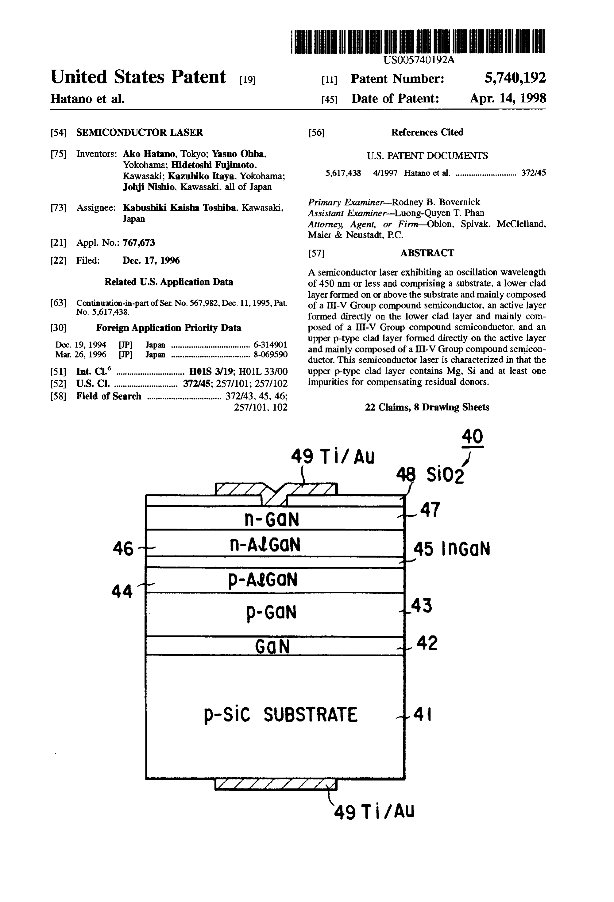
p-SiC SUBSTRATE 4
Page 2
Drawing sheet — no readable text.
Page 3
Drawing sheet — no readable text.
Page 4
Drawing sheet — no readable text.
Page 5
Drawing sheet — no readable text.
Page 6
Drawing sheet — no readable text.
Page 7
Drawing sheet — no readable text.
Page 8
Drawing sheet — no readable text.
Page 9
Drawing sheet — no readable text.
Page 10
SEMCONDUCTOR LASER doped, the laser performance is lowered and, for the case of a semiconductor laser having an active layer as narrow as
CROSS-REFERENCE TO RELATED below 5 nm in thickness in particular, a greater adverse APPLICATIONS influence is exerted over an operating current.
This application is a continuation-in-part of U.S. patent In the case where the Mg doping amount is increased so
application Ser. No. 08/567,982, filed Dec. 11, 1995, now semiconductor to lower the resistance of a p-type cladding layer, a U.S. Pat. No. 5.617.438. laser principally composed of a Mg-doped III-V Group semiconductor is lower in the characteristics,
BACKGROUND OF THE INVENTION such as an efficiency of an emitting layer and, in the worst O case, the operation is not possible.
This invention relates to a semiconductor laser and to a semiconductor light-emitting element. In particular, this conductor In either case, if the Mg amount is increased in a semi invention relates to a semiconductor laser provided with a characteristics, layer, the semiconductor laser becomes poor in its p-type semiconductor film and a p-type layer and also to a thus failing to obtain adequate reliability. semiconductor light-emitting element provided with a 15 By the way, a nitride compound semiconductor such as p-type semiconductor film and a p-type layer. GaN has been attracting attention nowadays as amaterial for In recent years, a III-V Group compound semiconductor, example, a blue light-emitting diode or for a semiconductor laser. For such as GaAs, InP and GainAIP, can be grown, by a metal laser havea blue been light-emitting diode and a semiconductor realized by making use of the nitride organic chemical vapor deposition (MOCVD), with better compound semiconductor. This element.is featured as being controllability and has been extensively utilized as a con 20 formed of a so-called double hetero-structure wherein a stituent component for a semiconductor laser and a light light-emitting layer is sandwiched by a pair of materials, one emitting diode. of which having a p-type conductivity and the other having In the MOCVD method, Zn is generally used as a p-type an n-type conductivity. In this case, the energy band gaps of dopant for the III-V Group compound semiconductor and, the p-type and n-type materials are larger than that of the being used as a p-type dopant for the GaAs, exhibits a 25 light-emitting layer. It is required however in the formation substantially good doping characteristic. If, however, Zn is of a p-type nitride compound semiconductor layer to used as a dopant for a p-type containing III-V Group undergo a step of electron ray irradiation or of thermal compound semiconductor, such as InP and GainAlp, the annealing after the p-type nitride compound semiconductor quantity of Zn that can be incorporated into the compound layer has been grown by way of an MOCVD as described for semiconductor is limited and it has been difficult to dope Zn 30 instance in Japanese Patent Unexamined Publication H/2- in a desired amount. Further, the activation degree of Zn is low and the diffusion of it in a layer is fast, resulting in poor 257679
or Japanese Patent Unexamined Publication H75
However, these steps may bring about a cause for controllability. generating a crystal defect such as a nitrogen void which is The elements Be and Mg for example may be considered 35 peculiar to a nitride compound semiconductor. Due to these as a p-type dopant in place of Zn. The element Be exhibits reasons, even though the formation of a p-type nitride a good characteristic as a p-type dopant in a molecular beam compound semiconductor layer has been realized, it is still epitaxy (MBE) method. impossible to increase the concentration of p-type carrier, However, the organic Be compound is strongly toxic and and hence to lower the resistance of element as well as to it is very difficult to use it as the dopant in the MOCVD lower the contact resistance of electrodes. method. On the other hand, a straight chain type organome As explained above, the conventional process of manu tallic compound of Mg., such as dimethylmagnesium and facturing a p-type compound semiconductor layer is diethylmagnesium, is not toxic in nature, but very strong in involved with a phenomenon which interferes with the aim its self-association and never occurs in single form. For this of the p-type compound semiconductor. Further, it has been reason, the Mg-containing straight chain type organometal 45 difficult according to the conventional method to form a lic compound is not suitable as a doping agent. p-type nitride compound semiconductor layer having a high Recently, biscyclopentadienylmagnesium (Cp2Mg) rela carrier concentration.
tively high in vapor pressure has been used as a Mg-doping material. However, the material CpMg is deposited as a BRIEF SUMMARY OF THE INVENTION residual one in a crystal growing apparatus and exhibits a Accordingly, an object of the present invention is to memory effect so that the doping control is very difficult. In provide a compound semiconductor layer having a p-type spite of the fact that a three-orders-of-magnitude-greater compound semiconductor layer of high carrier concentra concentration variation is required in a 0.1 in film thickness tion.
for a double heterosturcture (DH) laser device, such a sharp Another object of this invention is to provide a semicon concentration variation cannot be ensured at the present 55 ductor light-emitting element having a p-type compound time. In order to enhance the vapor pressure, the methyl semiconductor layer of high carrier concentration. group-attached cyclopentane ring material "bismethylcyclo pentadienyl magnesium" (CH)CpMg is known as one Namely, according to the present invention, there is example of a dopant and, even in this case, no sharp provided a semiconductor laser exhibiting an oscillation Mg-concentration variation is obtained at a doped-to wavelength of 450 nm less and comprising:
undoped interface. a substrate;
In order to reduce a resistivity of a predetermined semi a lower clad layer formed on or above the substrate and conductor layer, more amount of Mg has to be doped as a mainly composed of a III-V Group compound semi p-type dopant. In order to obtain a resistance value of, for conductor;
example, about 0.5 Q.cm to 10 O-cm, the Mg has to be 65 an active layer formed directly on the lower clad layer and doped at a concentration amount of about 5x10fcm to mainly composed of a III-V Group compound semi 5x10"/cm. In the case where more amount of Mg is so conductor; and
Page 11
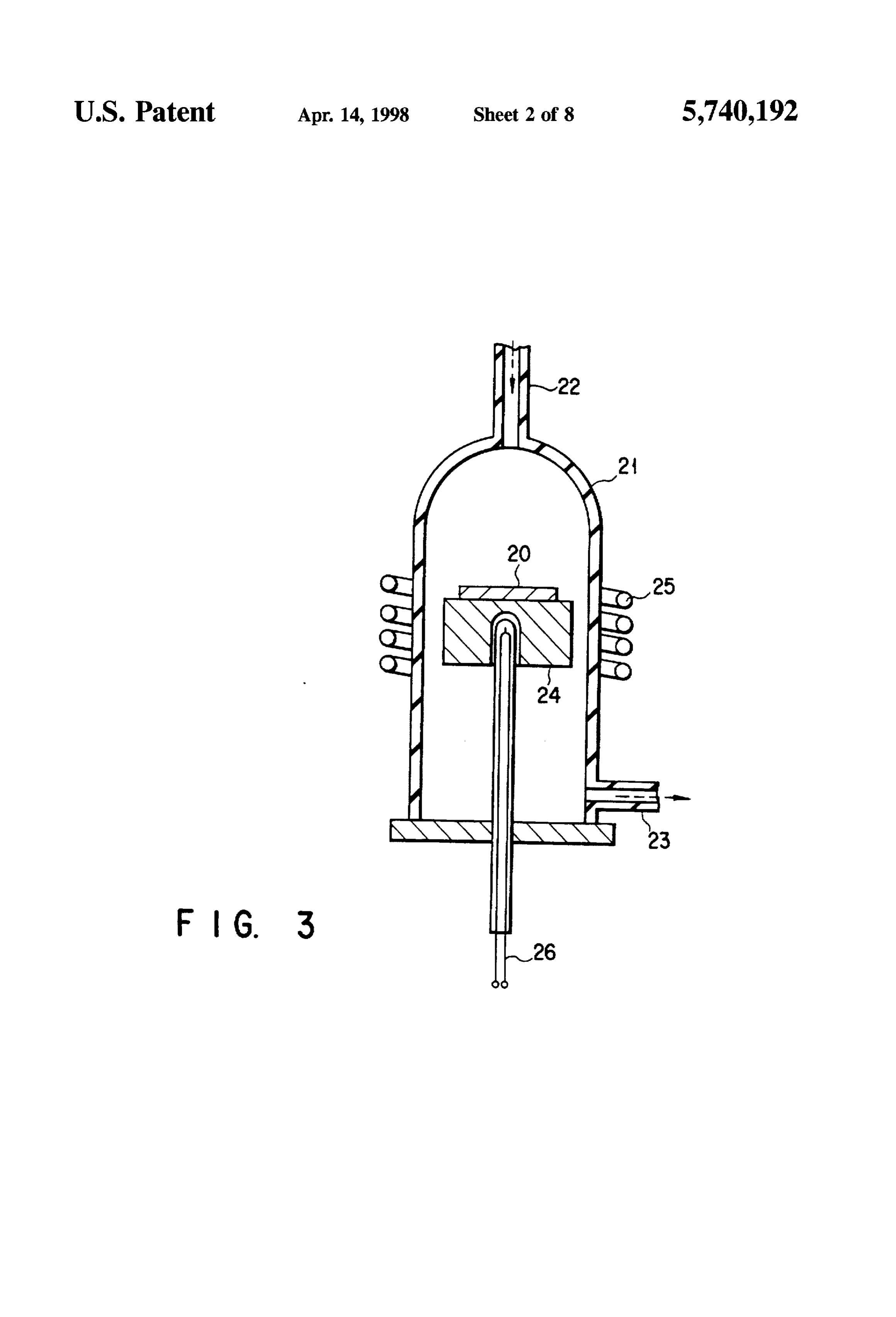
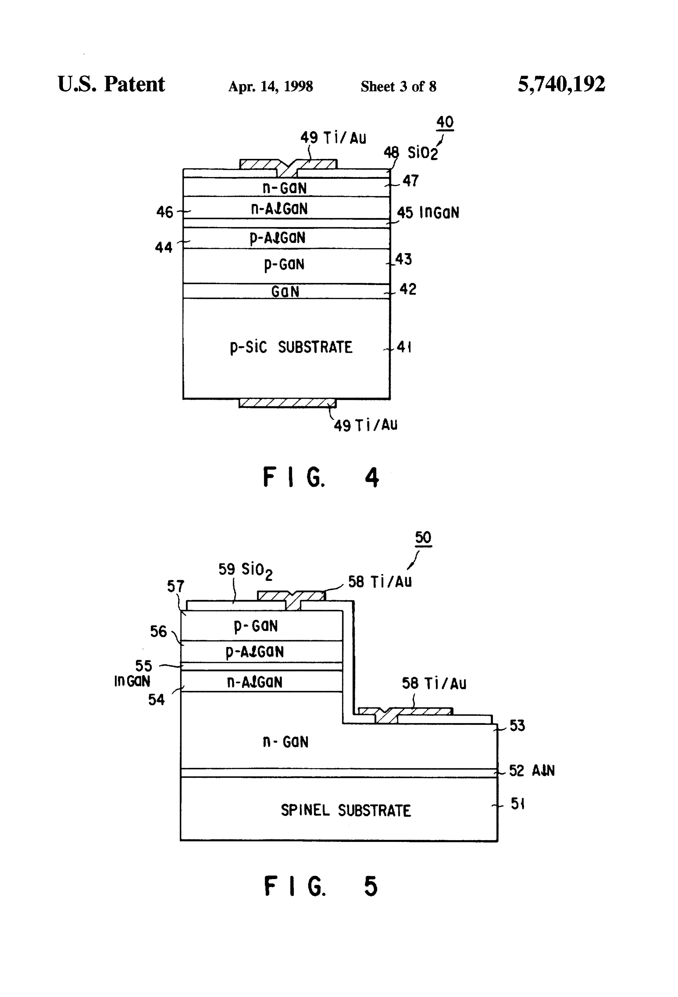
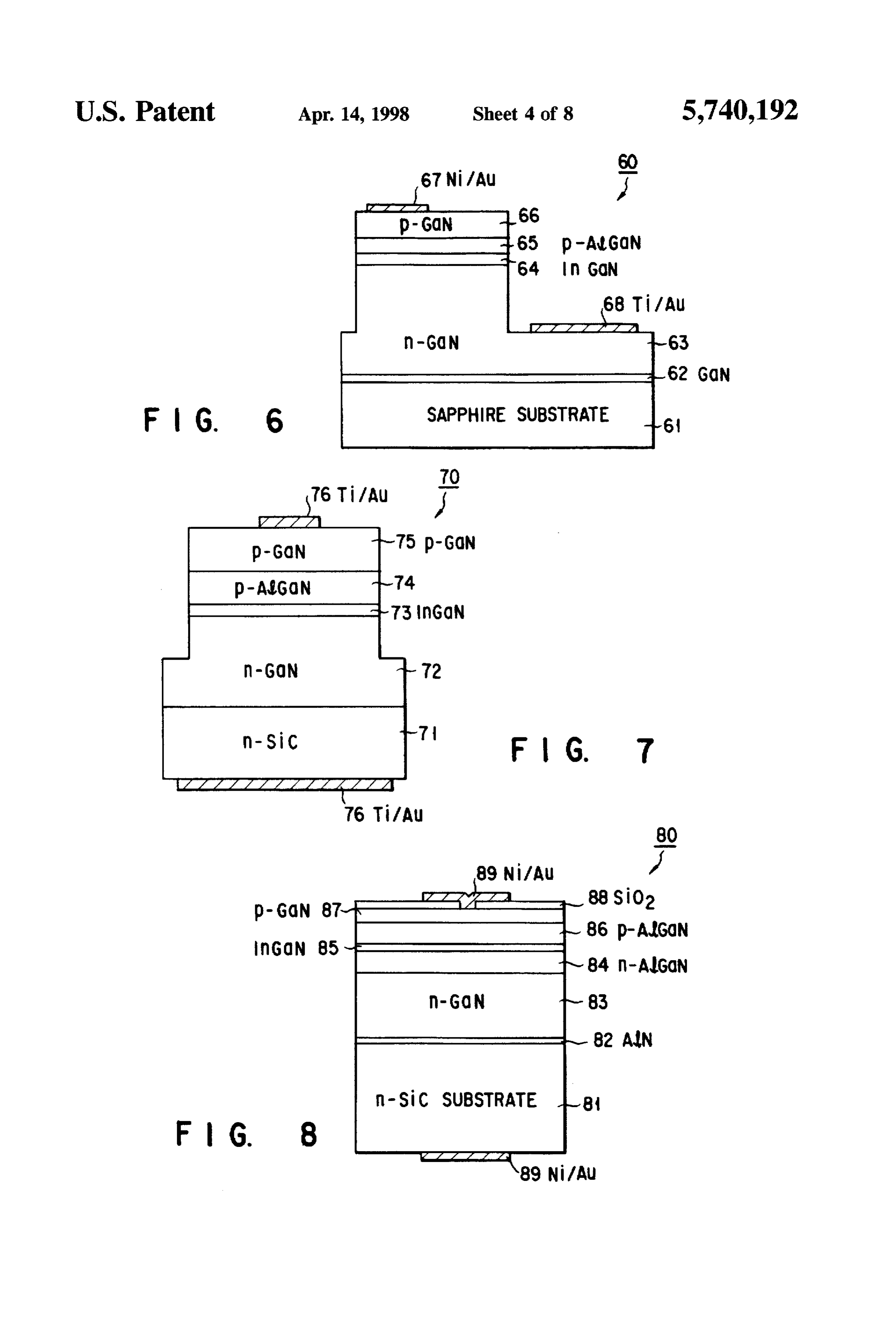
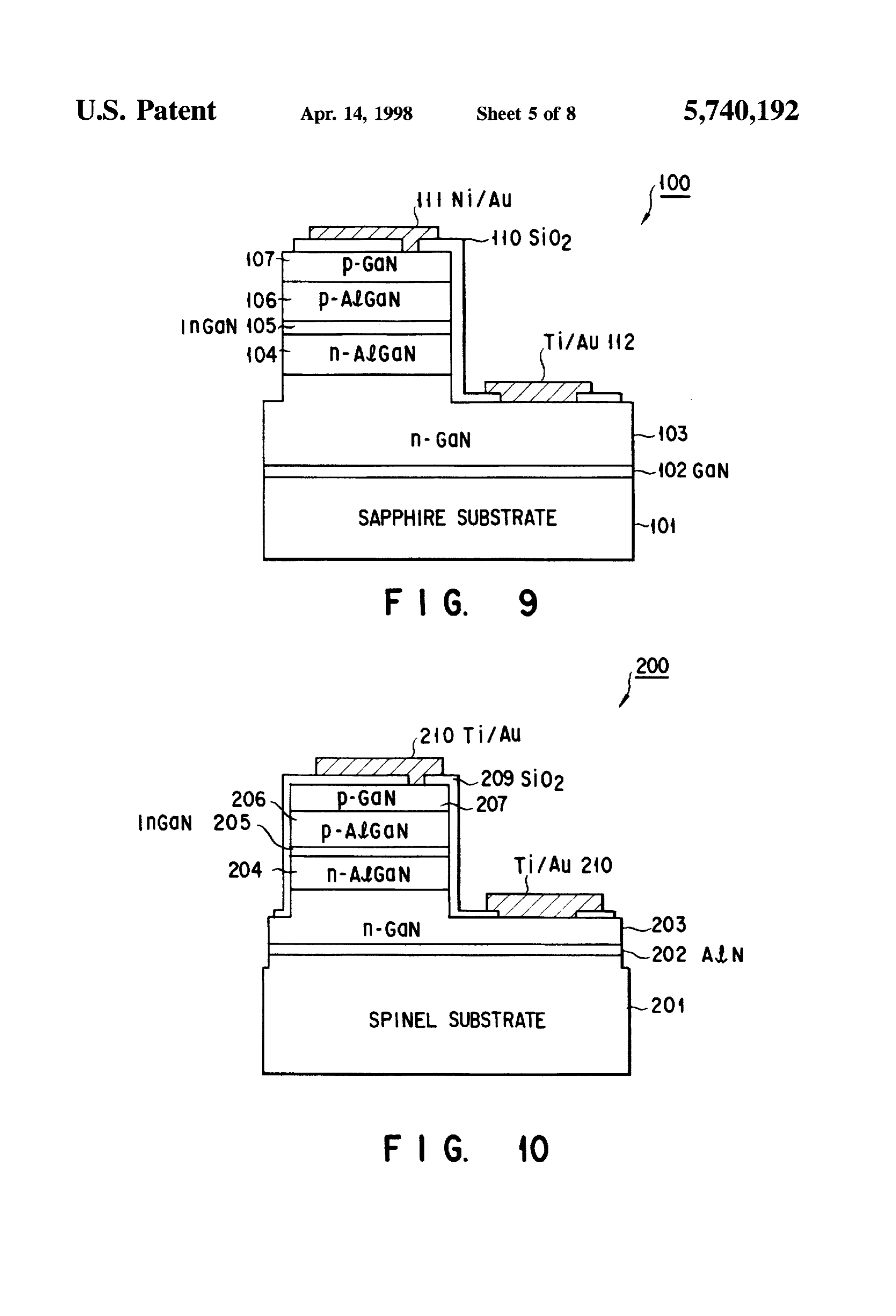
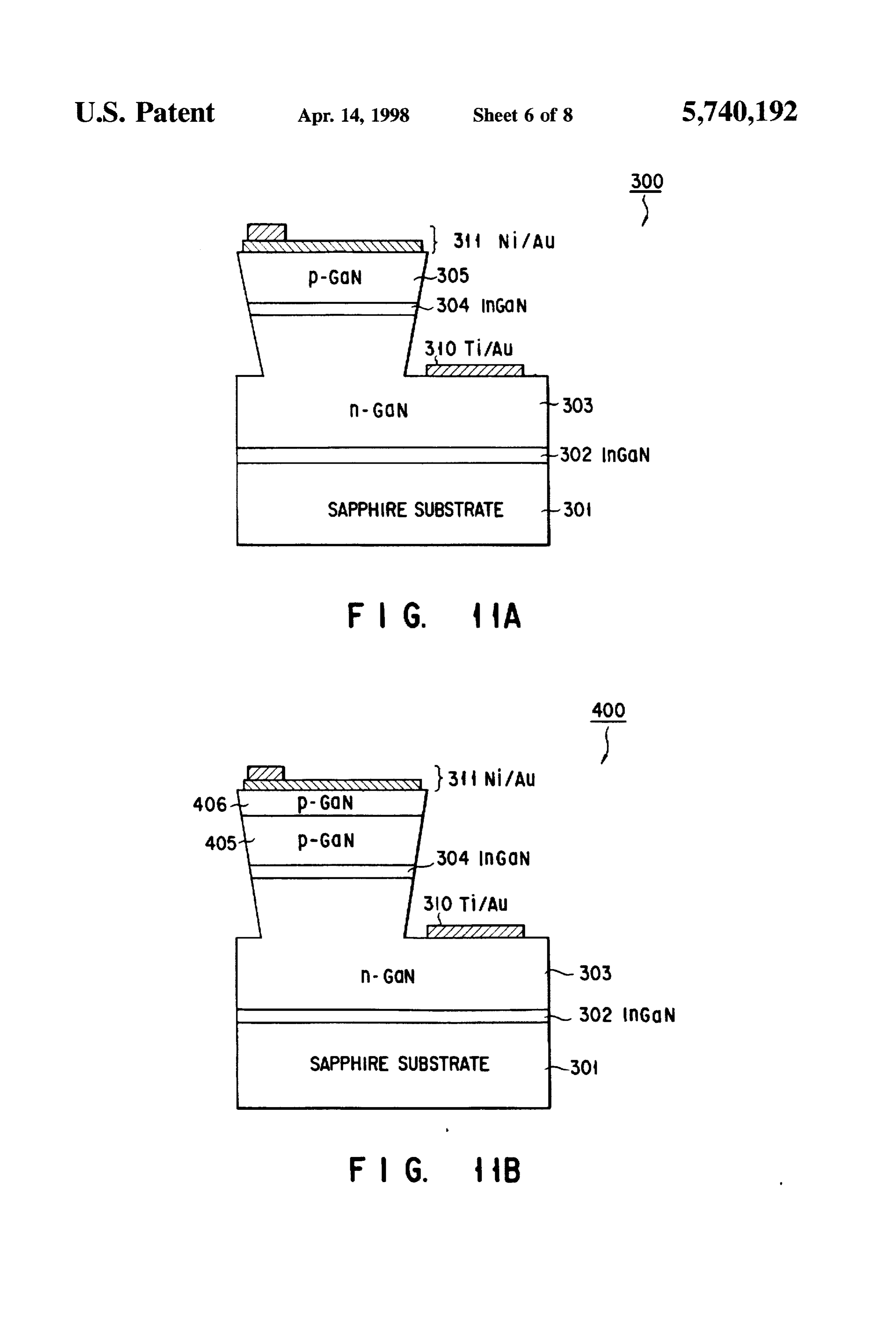
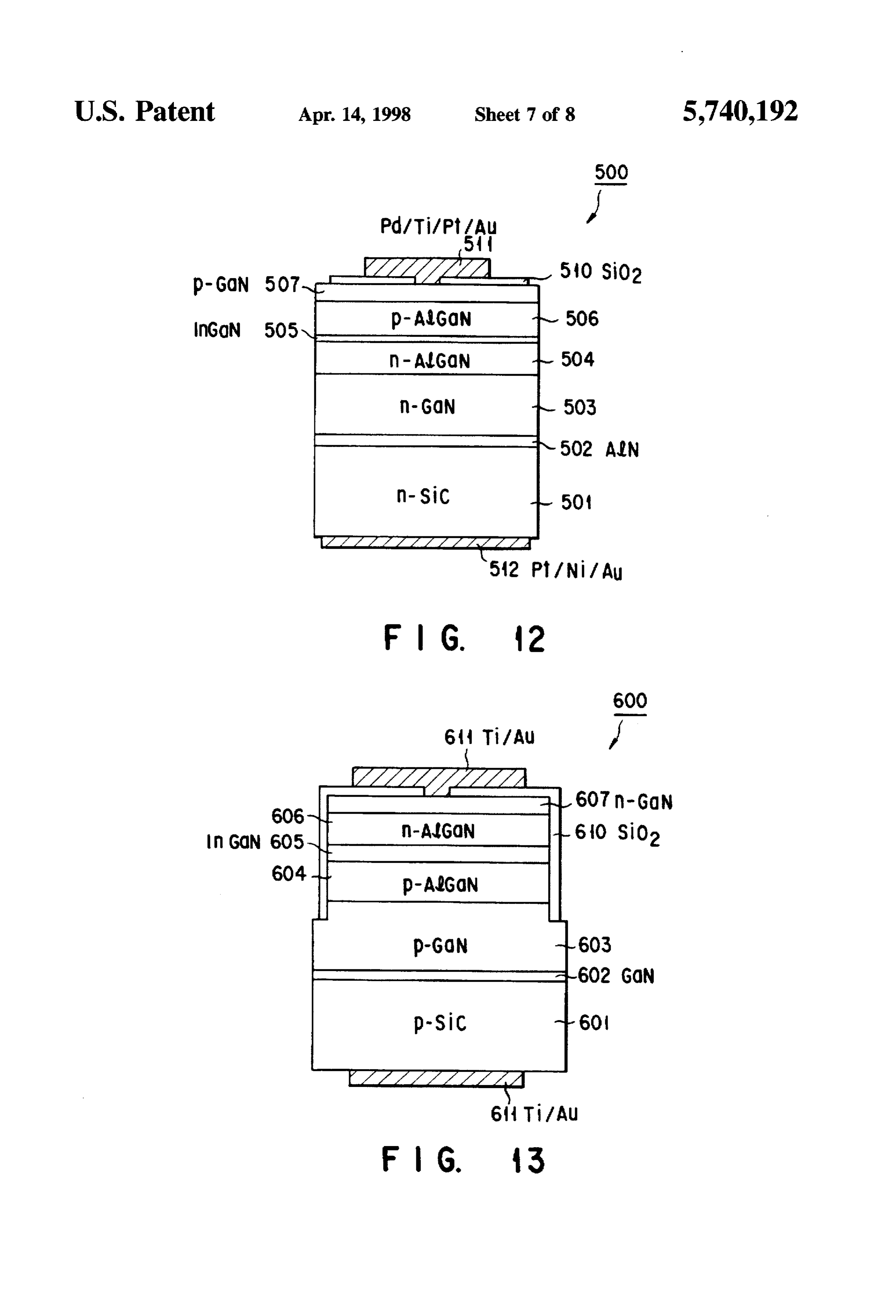
an upper p-type clad layer formed directly on the active FIG. 3 is a diagrammatic view showing a crystal growing layer and mainly composed of a III-V Group compound apparatus as used in the manufacture of the embodiment; semiconductor; FIG. 4 is a cross-sectional view of a semiconductor laser the upper p-type clad layer containing Mg. Si and one or according to another embodiment of this invention; more impurities for compensating residual donors. FIG. 5 is a cross-sectional view of a semiconductor laser According to the present invention, there is further pro according to still another embodiment of this invention; vided a semiconductor laser exhibiting an oscillation wave FIG. 6 is a cross-sectional view of a light-emitting diode length of 450 nm or less and comprising: according to another embodiment of this invention; a substrate; O FIG. 7 is a cross-sectional view of a light-emitting diode a lower clad layer formed on or above the substrate and according to another embodiment of this invention; mainly Composed of a III-V Group compound semi FIG. 8 is a cross-sectional view of a semiconductor laser conductor; according to still another embodiment of this invention; an active layerformed directly on the lower clad layer and FIG. 9 is a cross-sectional view of a semiconductor laser mainly composed of a III-V Group compound semi 15 according to still another embodiment of this invention; conductor; and FIG. 10 is a cross-sectional view of a semiconductor laser an upper p-type clad layer formed directly on the active according to still another embodiment of this invention; layer and mainly Composed of a III-V Group com FIG. 11A and 11B respectively shows a cross-sectional
view of a light-emitting diode according to still another the upper p-type clad layer containing Mg and one or embodiment of this invention;
more acceptor impurities for compensating residual FIG. 12 is a cross-sectional view of a semiconductor laser donors. according to still another embodiment of this invention; According to the present invention, there is further pro FIG. 13 is a cross-sectional view of a semiconductor laser vided a III-V Group compound semiconductor light 25 according to still another embodiment of this invention; emitting element having a p-n junction and being capable of emitting light through a recombination of electrons and FIG. 14 is a cross-sectional view of a semiconductor laser holes: according to still another embodiment of this invention. the p-type layer containing Mg and C as an acceptor DETALED DESCRIPTION OF THE impurity for compensating residual donors, the concen 30 INVENTION tration of the carbon atom being 8x10"/cm or more.
According to the present invention, there is further pro The inventors have conceived that the lowering in reli vided a semiconductor light-emitting element comprising: ability of a semiconductor laser that will be caused by the a substrate comprising a p-type compound semiconduc doping of a greater quantity of Mg into a III-V Group tor; 35 compound semiconductor layer is due to the diffusion of Mg a p-type GaN-based semiconductor layer formed on or interface into an associated layer and no formation of any sharp above the p-type compound semiconductor substrate; between a doped and an undoped layer. As a result of strenuous researches into the causes, the inventors have a light-emitting layer formed directly on the p-type GaN found it possible to suppress the diffusion of the Mg in the based semiconductor layer and composed of a GaN presence of Si in the doped layer. That is, in order to reduce based semiconductor. and the resistance of a specific semiconductor layer to nearly a an n-type GaN-based semiconductor layer formed predetermined extent, it is required that an amount of Mg directly on the light-emitting layer; contained in that layer be set to be of the order of not less the p-type GaN-based semiconductor layer containing than 10"/cm. In this case, the Mg is diffused across an Mg, Si and one or more impurities for compensating 45 interface with an adjacent layer. For this reason, no sharp residual donors. interface is created between the doped and the undoped Additional objects and advantages of the invention will be layer, resulting in lowered reliability being caused on a set forth in the description which follows, and in part will be semiconductor laser.
obvious from the description, or may be learned by practice In the semiconductor laser of the present invention, Si of the invention. The objects and advantages of the invention 50 together with Mg is present in a p-doped layer so that the may be realized and obtained by means of the instrumen diffusion of Mg in the p-doped layer can be suppressed. talities and combinations particularly pointed out in the Particularly by incorporating the amount of Si correspond appended claims. ing to that of Mg into the doped layer it is possible to more BRIEF DESCRIPTION OF THE SEVERAL effectively suppress the diffusion of Mg. Where not less than VIEWS OF THE DRAWING 55 2x10"/cm of Si is contained in a III-V Group compound semiconductor layer, even if not less than 5x10/cm of Mg
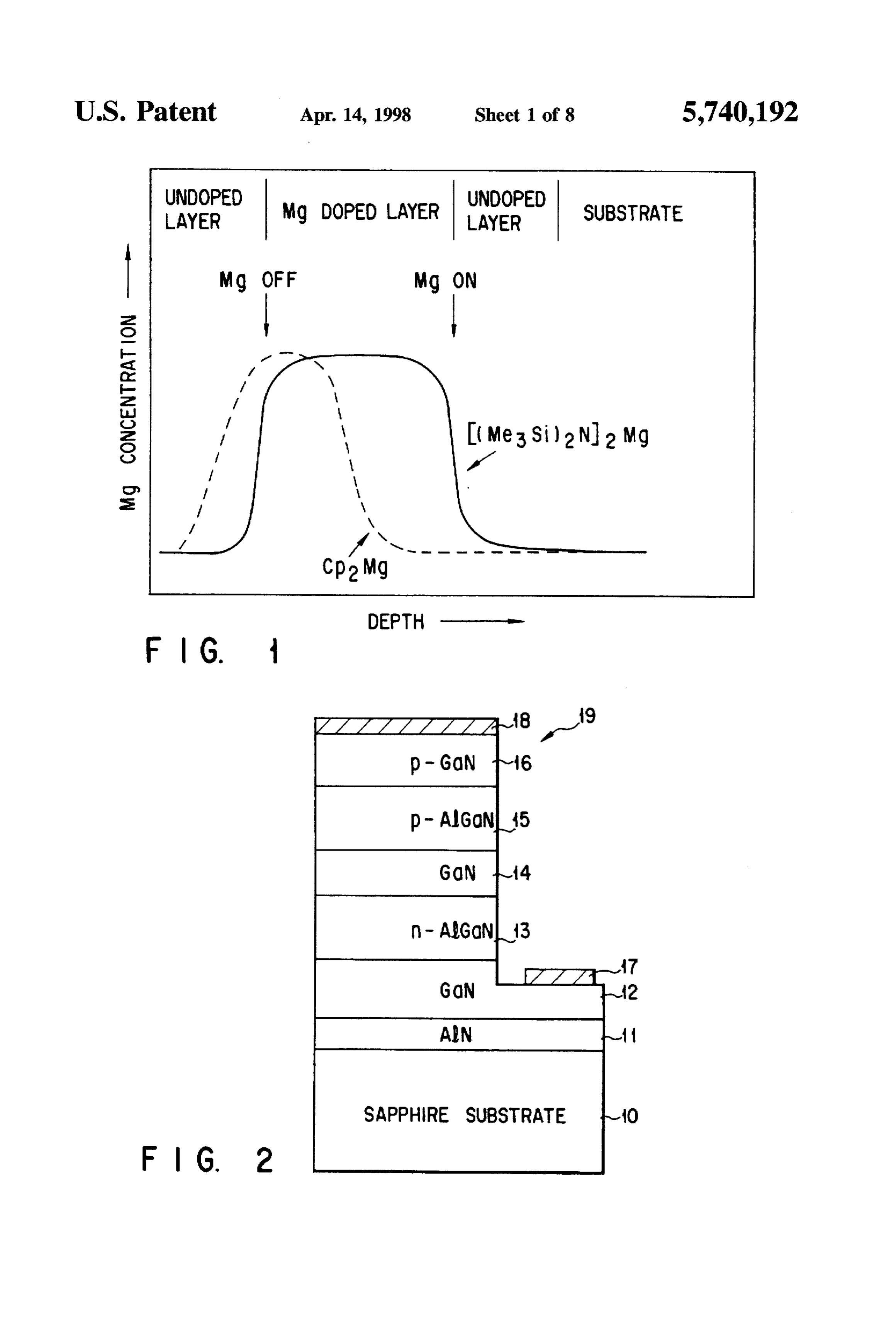
The accompanying drawings, which are incorporated in is contained in this layer, the diffusion of Mg into a neigh boring layer is suppressed. That is, a desired resistance is and constitute a part of the specification, illustrate presently preferred embodiments of the invention and, together with obtained by doping a larger amount of Mg and by suppress the general description given above and the detailed descrip ing the diffusion of Mg by Si, it is possible to ensure a sharp tion of the preferred embodiments given below, serve to interface between the doped and the undoped layer. With the explain the principles of the invention. employment of a semiconductor laser having such semicon FIG. 1 is a view showing a relation of a Mg concentration ductor components as main constituents, it is possible to profile to a depth direction when Mg is doped into GaN prevent the semiconductor laser from being lowered in layer; 65 reliability.
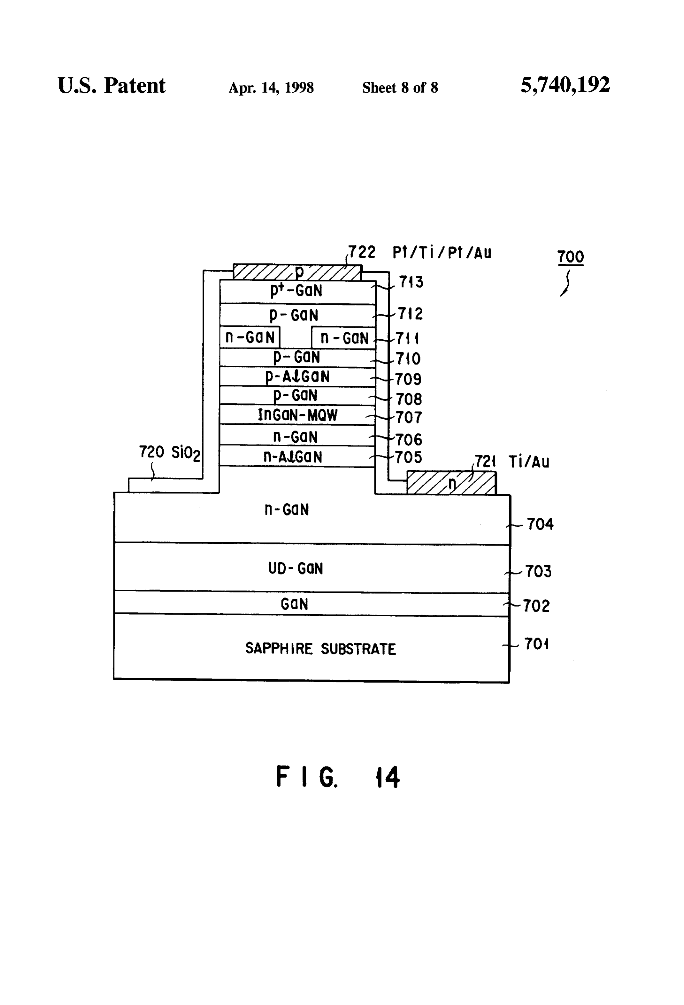
FIG. 2 is a cross-sectional view showing a semiconductor p-typeAccording to the present invention, if Mg is doped as a laser according to one embodiment of the present invention; dopant into the III-V Group compound
Page 12
semiconductor, two kinds of gases can be used as feed gases, doped layer and hence to achieve the effective doping of Mg. one being a compound gas containing the Si and the other a The trimethylsilyl group in the compound above is of such Compound gas containing the Mg. As the compound gas a type as to have three methyl groups attached to an Siatom containing the Si, use may be made of an Sihydride such as and hence is bulkier, steric and well symmetrical. For this SiH4 and SiH as well as an organometallic Si component reason, the MeSi-group, combining with another substance, such as Si(CH), while, on the other hand, as the compound produces a stable substance.
gas containing the Mg use may be made of CPM.g. bis By forming a p-type cladding layer of the III-V Group (methylcyclopen tadienyl) magnesium, bis compound semiconductor by the MOCVD method with the (ethylcyclopentadienyl)magnesium, etc. use of such an organic Mg compound as a feed gas, Si The flow rate of the feed gas containing the Si can be 1) together with Mg is incorporated in the doping layer. This Si determined in accordance with that of the feed gas contain suppresses the Mg diffusion whereby a sharp interface is ing the Mg. Since the amount of Si corresponding to that of created between the doped and the undoped layer. Mg needs to be present so as to suppress the diffusion of the Since the organic Mg compound has an adequate high Mg in the III-V Group compound semiconductor layer, an vapor pressure and no memory effect, the sharpness of the amount of Si fed is selected in accordance with a desired 15 doped-to-undoped layer interface can be more enhanced and amount of Mg. If, for example, the amount of carrier fow hence doping can be achieved with good reproducibility. through CPMg at 0°C. is fed as the Mg feed at a rate of 10 It is considered that the incorporation of Si into the to 100 cc/min., then the amount of SiH is also fed as the Si compound semiconductor as set out above occurs even if use feed, preferably, at a rate of -10 to 100 cc/min. with a is made of two kinds of feed gases, one containing Si and the concentration of 10 ppm. other containing Mg.
In the manufacture of a semiconductor laser of the present That is, a highly reliable semiconductor laser can be invention having a predetermined compound semiconductor obtained by incorporating Si into a cladding layer of the layer containing the Si and Mg, use may be made, as a feed p-doped III-V Group compound semiconductor layer, gas, of a compound Containing the Mg and Si. Effective as such a compound is an organic Mg compound having a bond 25 The present invention will be explained below by way of with three methyl groups attached to an Si atom as repre examples.
sented by an MeSi group. EXAMPLE I Explanation will be given below about the organic Mg compound. The organic Mg compound contains the Mg and Using the material (MeSi)NMgas a feed gas, Mg was Si and hence only one kind of feed gas is required and, in doped into a GaN layer by virtue of an MOCVD method and addition, the following advantages are also obtained. The measurement was made by an SIMS analytical method on a inventors have considered a CaMg memory effect not as Mg concentration profile in a depth direction of the GaN being an essential problem of the Mg compound but as being layer. A result of measurement is shown in FIG. 1. For a problem specific to the Mg compound containing a cyclo comparison, Mg was doped into a GaN layer with the use of pentane ring. It is, therefore, possible to avoid the memory 35 the material CpMg and then measurement was similarly effect if the Mg compound free from any cyclopentane ring made on the Mg concentration profile, the result of which is used as the feed gas. However, a straight-chain type alkyl being shown in FIG. 1.
Mig compound, being normally used as a feed gas in an As shown in FIG. 1, when the material CpMg was used MOCVD process, exhibits a strong self-associative property as the feed gas, Mg was not immediately incorporated into as set out above and does not occur in single form. a desired layer even if the feed gas starts flowing. Further, The inventors have found that, of the organic Mg Mg was slowly taken into that layer even if the supply of Mg compounds, those having a bulkier and well-symmetrical was stopped.
group occur as a single form and as a compound having an When, on the other hand, the material (MeSi)NMg adequately high vapor pressure. The material (MeSi)N) 45 was used, Mg was doped substantially at a constant rate into 2Mg is considered as one of such compounds and can ensure the doped layer while leaving a somewhat tail curve at a rise an adequate vapor pressure because its melting point is 116° and a fall in the level of Mg.
C. Therefore, the material (MeSi)NlMg is particularly It is to be noted that, in the case of (MeSi)NMg, Si preferable as a p-type dopant. together with Mg was incorporated into the doping layer in This Mg compound has a structure represented by the 50 substantially the same amount and that the concentration following formula (1). profile was sufficiently sharp. As evident from FIG. 1, a sharp interface is created (1) between a doped layer and an undoped layer by allowing Si.
together with Mg, to be incorporated into the doped layer.
55 FIG. 2 is a cross-sectional view showing a semiconductor laser according to a first embodiment of the invention. A first
This compound exhibits a marked advantage as a doping buffer layer 11 of AlN (10 nm), a second buffer layer 12 of material when Mg is doped fin the III-V Group compound GaN (1.0 m), an Si-doped n-type cladding layer 13 of semiconductor containing N. It is generally considered that, AlGaN (1.0 m), an active layer 14 of GaN (0.05 m), an if Mg is doped in the III-V Group compound semiconductor Mg-doped p-type cladding layer 15 of AlGaN (1.0 m) and with N contained therein, hydrogen (H) together with Mg is an Mg-doped p-type contact layer 16 of GaN (0.5 m) are incorporated into the semiconductor. With hydrogen mixed formed over the surface of a sapphire substrate 10 in a into a doping layer, the activation degree of the p-type sequential way. Further, an Au/TiAl electrode 17 and Au?Ni dopant is lowered and it is therefore possible to minimize the electrode 18 are provided on the upper surface of the second mixing of H into the doping layer. The compound repre 65 buffer layer 12 and p-type contact layer 16, respectively. sented by the formula (1) above has a Mg-N bond in its own FIG. 3 is a diagrammatical view showing a crystal grow structure and it is possible to suppress the mixing of H in the ing apparatus using a method for carrying out the present
Page 13
invention. Reference numeral 21 in FIG. 3 shows a reaction Au/Ni electrode 18 is by vapor deposition on the surface of tube made of quartz. A feed gas mixture is introduced via a the contact layer 16 to obtain a semiconductor laser 19 of the gas supply inlet 22 into the reaction tube 21. The gas mixture present invention as shown in FIG. 2. The semiconductor laser of such an arrangement has an oscillation wavelength in the reaction tube 21 is exhausted via a gas exhaust outlet of 450 nm.
23. A susceptor 24 made of carbon is located in the reaction 5 tube 21 and dielectrically heated by a high frequency coil 25. MgConsideration and Si in the is given below about the concentration of p-doped layer in the semiconductor laser
A sample substrate 20 is placed on the susceptor 24 and the of the first embodiment. It is considered that, if a 1.0 temperature of the substrate 20 is measured by a thermo um-thick p-doped layer is formed in accordance with the couple 26 and the measured temperature is controlled by above-mentioned process step with the flow rate of the Mg another device, not shown. 10 feed at 0°C. with 50 cc/min., an amount of Mg and of Si in
A method of manufacturing a semiconductor laser of a the p-type cladding layer is 5x10'/cm and 3x10'/cm, structure as shown in FIG. 2 will be briefly explained below respectively. In this case, an amount of Mg in a 1.0 um-film with the use of the growth device of FIG. 3. thickness varies by three-orders-of-magnitude at a boundary First, a substrate is placed on the susceptor and, through 15 between the p-type cladding layer and the active layer. the introduction of an Higas into a chamber, heated to 1100° Even where the active layer (undoped layer) underlying C. and the surface of the substrate is cleaned. Then, the the doped layer is not more than 5 nm thick, the doping substrate temperature is dropped to 450° to 900° C., fol amount can be controlled with adequate accuracy. lowed by the replacement of the H gas with an Calculation was made on the amount of Mg and of Si in N-containing organic compound, such as an NH gas or 20 the p-doped layer and variation of the Mg amount at the (CH)NH2. Together with the N-containing organic interface between the p-doped and the undoped layer, the compound, an organometallic compound corresponding to results of which being shown in Table 1 below. layers to be grown is introduced into the chamber and respective layers are grown over the substrate surface. TABLE 1. In the formation of semiconductor layers on the substrate. 25 Sample Si concen- Mg concen- Change in Mg an organometallic All compound, such as Al(CH) or No. tration tration concentration Al(CH) is introduced into the chamber to form a first 1 3 x 10 6 x 10⁹ 2 times buffer 11 containing AlN on the substrate 10. 2 3 x 10⁷ 5 x 10⁸ 5 times Then, an organometallic Ga compound, such as Ga(CH) 3 1 x 10 2 x 10⁹ 5 times or Ga(CH), is introduced into the chamber to form a 30 second buffer layer 12 containing GaN. As shown in Table 1, when an amount of Siin the p-doped A first cladding layer 13 containing AlGaN is grown on layer is less than 2x10"/cm. a variation in an Mg amount the surface by introducing an n-type doping feed in addition per 0.1 m in its interface with the undoped layer is only a to the organometallic Al compound and organometallic Ga half. That is, it is not possible to obtain a sharp doping of Mg compound. As the n-type doping feed use can be made of an 35 in the p-type cladding layer, organometallic Si compound, such as an Sihydride such as When an amount of Mg in the p-doped layer is less than SiH or organometallic Si compound such as Si(CH). 5x10'/cm, a desired resistance cannot be obtained though An active layer 14 is grown on the resultant surface, like a diffusion length is not more than 0.1 m. In order to the second buffer layer, by introducing the organometallic maintain the characteristic of the doped layer, a concentra Ga compound such as Ga(CH) or Ga(CH) into the tion equal to or more than 1x10"/cm of Mg is required. If, chamber. It is to be noted that In may be added to the GaN on the other hand, Si is contained in the doped layer. Mg is active layer 14 so as to narrow a band gap in the GaN active diffused to a neighboring layer, thus failing to obtain any layer 14. In this case. In can be added to the active layer by sharp interface.
introducing an organometallic In compound such as 45 Where Si in the p-doped layer is equal to or more than In(CH) or In(CH) at a molecular ratio of In source to Ga 2x10"/cm, a variation in an amount of doped Mg at the source in vapor phase of 5% to 100% for example. interface with the undoped layer is five times per 0.1 um. A cladding layer 15 containing AlGaN is grown on the From this, it has been found possible to obtain a very sharp resultant surface by introducing a p-type doping feed in interface. Even in this case, the resistance of the p-doped addition to the organometallic Al compound and organome 50 layer is not more than 1 Q.cm, a value adequate to a tallic Ga compound. As a p-type doping feed, use can be semiconductor laser.
made of a trimethylsilyl group-containing organometallic Since, according to the present invention, Si is incorpo Mg compound such as (MeSi)2N),Mg, (MeSi)CH2Mg rated into a p-type AlGaN cladding layer of DH structure, it and (MeSi),Mg. is possible to achieve a sharp doping of Mg and hence to A contact layer 16 is grown on the resultant surface by 55 predict a DH laser of excellent performance. introducing the organometallic Ga compound such as Since, in particular, the organic Mg compound having an Ga(CH) or Ga(CH) into the chamber. As the p-type MeSi-group is used as an AlGaN p-type dopant, the sharp doping feed for the contact layer 16, use is made of the doping of Mg can be achieved at the p-type AlGaN cladding trimethylsilyl group-containing organic Mg compound. layer of DH structure, thus making it possible to manufac In this way, the first buffer layer, the second buffer layer. ture a DH laser of excellent performance. the first cladding layer, the active layer, the second cladding Since, according to the present invention, not only Mg but layer and the contact layer are sequentially formed over the also Si is incorporated into the AlGaN cladding layer, it is semiconductor substrate as set out above and a resultant predicted that the sharp concentration change of Mg can be semiconductor structure is selectively etched to remove achieved and a DH laser of excellent performance can be predetermined areas. 65 obtained.
An Au/TiAl electrode 17 is formed by vapor deposition on Since, in particular, the organic Mg compound having an the exposed surface of the second buffer layer 12 and an MeSi group is used as the Mg feed, a sharp doping can be
Page 14
achieved at the cladding layer-to-active layer interface and EXAMPLE I-1 at the same time the development of defects and distortion FIG. 4 illustrates a cross-sectional Structure of a semi can be suppressed at the surface of the cladding layer and it conductor laser 40 according to this invention. The laser 40 is possible to manufacture a DH laser of excellent perfor comprises a p-type SiC substrate 41 on which a GaN buffer
The present invention is not restricted to the above layer 42 having a thickness of 10 nm is formed for allevi mentioned respective embodiments. Although, in the ating a mismatching of lattice. On this GaN buffer layer 42 embodiment, the trimethylsilyl group-containing organic are further deposited a p-type GaN layer 43 (2 m in Mg compound has been used as a Mg feed gas in an thickness), a p-type AlGaN layer 44 (500 nm in thickness), MOCVD process, use can be made of any MeSi group an IngaN active layer 45 (100 nm in thickness), an n-type containing organic Mg compound. AlGaN layer 46 (500 nm in thickness) and an n-type GaN The materials of the compound semiconductor layer as set layer 47 (300 nm in thickness) in the mentioned order. Each out in connection with the embodiment are not restricted of these layers are made into a p-type or an n-type conduc thereto and a proper modification can be made in accordance tivity by the addition of a suitable impurity or impurities. with a specification used. Various changes and modifications 15 Specifically, the impurities added to the p-type GaN layer 43 can be made without departing from the spirit and scope of and the p-type AlGaN layer 44 are Mg and C. On the other the present invention. hand, the impurity added to the n-type AlGaN layer 46 and According to the present invention, as set out above in the n-type GaN layer 47 is Si. Among these impurities. C more detail, a highly reliable semiconductor laser can be (carbon) in the p-type layers 43 and 44 functions to form a obtained by incorporating Mg and Si into the p-doped III-V 20 deep acceptor level thereby compensating the residual Group compound semiconductor. donors, thus making it possible to achieve an increased Since a MeSi-group-containing organic Mg compound is carrier concentration through the addition of Mg which employed as the Mg material in the MOCVD process forms a relatively shallow acceptor level.
according to the method of the present invention, it is Additionally, a Ti/Au laminate electrode 49 which is possible to ensure the growth of a compound semiconductor defined layer structure excellent in a doping sharpness of Mg with SiO filminto48aisstripe
deposited on the n-type GaN layer 47. The good reproducibility and with controllability of Mg concen same kind of Ti/Au laminate tration. It is expected that the present method contributes thickness as mentioned aboveelectrode 49 having the same is also formed on the back much to the improvement of the characteristic of a semi surface of the p-type SiC substrate 41. conductor laser and of a device using a compound semicon Next, the method of manufacturing the semiconductor ductor such as a light-emitting diode. 30 laser 40 will be explained as follows.
EXAMPLE I This semiconductor laser 40 was manufactured by way of
The present inventors have made an extensive study on the known metal organic chemical vapor deposition the cause of failure to obtain a p-type nitride compound (MOCVD) method. The raw materials employed in this case Semiconductor having a high carrier concentration and suc 35 were organometallic raw materials such as trimethylgallium ceeded to obtain the following findings. Namely, it has been (TMG), trimethylaluminum (TMA), trimethylindium (TMI) assumed that a p-type nitride compound semiconductor and biscyclopentadienylmagnesium (Cp2Mg); and gaseous should indicate a p-type conductivity only if it is added with raw materials such as ammonia, silane and propane. As a Mg exhibiting inherently a nature of acceptor as a dopant. carrier gas, hydrogen and nitrogen were employed. However, it has been impossible with an addition only of Mg First of all, the SiC substrate 41 was subjected to an to obtain a p-type nitride compound semiconductor having organic washing and acid washing. Then, the resultant SiC a high carrier concentration because of the following two substrate 41 was mounted on a susceptor which was placed phenomena. First, since the nitride compound semiconduc in a reaction chamber of an MOCVD apparatus so as to be tor is liable to generate Ga entering into the nitrogen voids heated by means of a high-frequency wave. Then, the natural or an interstice of lattice, a high concentration of residual 45 oxide film formed on the surface of the SiC substrate 41 was donor will be resulted in the semiconductor layer of p-type. removed by subjecting it to a vapor-phase etching at a Secondly, the acceptor level of Mg of the nitride compound temperature of 1200° for about 10 minutes while allowing semiconductor is extremely deeper than the acceptor level hydrogen gas to flow at a flow rate of 20 l/min. at normal which has been commonly considered of the semiconductor. pressure.
Therefore, it has been found that by adding, together with 50 For the formations of semiconductor layers on this SiC Mg, one or more impurities which is ordinary irrelevant to substrate 41, the temperature of the SiC substrate 41 was the conversion top-type or an acceptor impurity to an nitride lowered down to 800° C., and hydrogen gas, nitrogen gas, compound semiconductor, the donor formed due to the ammonia gas and TMG were-allowed to flow for about 5 nitrogen void can be compensated. Namely, since it is minutes to form the GaN buffer layer 42. The flow rate of possible with the. addition of such an impurity to remove 55 each of hydrogen gas, nitrogen gas and ammonia gas was set any cause that has been an obstacle in the conversion of a to 5 l/min., and the flow rate of TMG was set to 30 cc/min. semiconductor to a p-type semiconductor by making use of Thereafter, the SiC substrate 41 was heated up to 1.100° Mg, the formation of a p-type crystal having a high carrier C. and kept at this temperature, and at the same time, concentration has become possible by the addition of Mg. hydrogen gas and nitrogen gas each being fed as a carrier As for an impurity for compensating the residual impu gas, ammonia and propane gas each being fed as a feed gas, rities and for realizing a crystal of high carrier concentration and TMG and CpMg each being fed as an organometallic or as for an acceptor impurity, an impurity which is deep in raw material were allowed to flow for about 30 minutes, terms of energy is preferable for use. By the employment of thereby to form the p-type GaN layer 43. In this case, the such an impurity, the capture cross section of the crystal canflow rate of each carrier gas was set to 5 l/min., and the flow be enlarged and a large quantity of residual donors can be 65 rate of organometallic raw material was set to 30 cc/min. compensated with an addition of small amount of the The flow rates of ammonia and propane were set to 5 l/min. impurity. and 10 cc/min.., respectively. Then, additional TMA was
Page 15
allowed to flow at a flow rate of 100 cc/min. for about 8 layer 52 having a thickness of 50 nm is formed. On this AlN minutes together with these gases to form the p-type AlGaN wafer layer 52 are further deposited an n-type GaN layer 53 layer 44. (4 um in thickness), an n-type AlGaN layer 54 (500 nm in In the formation of the InGaN active layer 45, the thickness), an IngaN active layer 55 (100 nm in thickness). temperature of the SiC substrate 41 was lowered down to 5 aGaN p-type AlGaN layer 56 (500 nm in thickness) and a p-type 800° C. and kept at this temperature, and then nitrogen gas Each layer 57 (300 nm in thickness) in the mentioned order. of these layers are made into a p-type or an n-type (10 l/min.), ammonia gas (5 l/min.), TMG (30 cc/min.) and conductivity by the addition of a suitable impurity or impu TMI (200 cc/min.) were allowed to flow for about 10 rities. Specifically, the impurities added to the p-type AlGaN minutes.
10 layer 56 and the p-type GaN layer 57 are Mg and Ed. On the
Thereafter, the SiC substrate 41 was again heated up to other hand, the impurity added to the n-type GaN layer 53 1.100° C. and kept at this temperature. and at the same time, and the n-type AlGaN layer 54 is Si. Among these hydrogen gas and nitrogen gas each being fed as a carrier impurities, Cd (cadmium) in the p-type layers 56 and 57 gas, TMG and TMAeach being fed as an organometallic raw functions to compensate the residual donors. material, and ammonia gas and silane gas each being fed as 15 Additionally, a Ti/Au laminate electrode 58 which is a raw material gas were allowed to flow for about 8 minutes. defined thereby to form the n-type AlGaN layer 46. In this case, the SiO filminto 59 a stripe 10 pm in width by the presence of an is deposited on the p-type GaN layer 57. This flow rate of each carrier gas was set to 5 l/min... and the flow Ti/Au laminate electrode 58 is composed of a laminate rates of TMG and TMA were set to 30 cc/min. and 100 cc/min., respectively, The flow rates of ammonia and silane 20 Au film. The same akind structure comprising 50 nm thickTifilm and a 3 pm thick of Ti/Au laminate electrode 58 were set to 5 l/min, and 1 cc/min., respectively. Thereafter, having the same thickness as mentioned above is also all of these gases except the TMA were continued to flow for about one hour to form the n-type GaN layer 47. formed on the n-type GaN layer 53, which has been exposed by removing upper layers by means of etching.
Subsequently, the reaction chamber was cooled down to room temperature while allowing only nitrogen gas to flow 25 ofThis the semiconductor laser 50 was manufactured by means same MOCVD method as employed in the afore at a flow rate of 10 l/min... and then the wafer having these mentioned Example (I-1). As for the raw material for Cd to growth layers was taken out of the reaction chamber. be added to the p-type layers, dimethylcadmium (DMCd) Then, a SiO film 48 was formed up to a thickness of 0.5 was employed. If the concentration of Cd in the p-type um on the n-type GaN layer 47 by means of the known layers is too high, the carriers may be captured in the p-type thermal CVD method. This SiO film 48 was then subjected 30 regions thereby generating a light emission in the p-type to a photoetching process to form an opening having a width regions, thus preventing a sufficient injection of carriers into of 10 um therein. Thereafter, a Tifilm 50 nm in thickness and the active layer. Accordingly, the concentration of Cd should an Au film 3 m in thickness were successively formed on preferably be 1x10 cm or less. However, if the concen the upper surface of the opening by means of the known tration of Cd is too low, the effect expected from the addition vacuum vapor deposition method to form the Ti/Au laminate 35 of Cd cannot be obtained. Therefore, the concentration of Cd electrode 49. Another Ti/Au laminate electrode having the should preferably be 1x10 cm or more. When the same thickness as mentioned above was also formed on the concentration of Cd is set to a desirable range of from back surface of the SiC substrate 41. 1x10 cm to 1x107 cm the carrier concentration in the In this semiconductor element, carbon (C) is contained in p-type crystal indicated a maximum.
the p-type GaN layer 43 and the p-type AlGaN layer 44 at Since the spinal employed as a substrate in this example a concentration of 1x10" cm. This is because the con is poor in clearability and conductivity as compared with centration of carbon corresponds to the carrier concentration SiC, the threshold current becomes higher by about 20% as in the undoped GaN film. In this embodiment, although the compared with the aforementioned Example D-1. However, concentration of carbon in the p-type layers Was set to the since the spinel was free from a through defect which is above value, the concentration of, carbon should not be 45 peculiar to the SiC substrate, it was possible to enhance the construed to be limited to this value. Since the concentration output by about 30%.
of residual donor fluctuates depending on the conditions of EXAMPLE I-3 growing crystals, the concentration of carbon for compen sating the residual donor concentration may be suitably FIG. 6 illustrates a cross-sectional structure of a light determined according to the conditions of growing crystals. 50 emitting diode 60 according to this invention. The light However, in order to compensate the residual donor con emitting diode 60 comprises a sapphire substrate 61 on centration and at the same time to avoid carbon atoms from which a GaN buffer layer 62 (200 nm in thickness), an becoming any cause for an obstacle in the p-type crystal n-type GaN layer 63 (4 um in thickness), an InCaN light layers, the concentration of carbon should preferably be emitting layer 64 (100 nm in thickness), a p-type AlGaN limited to an range of from 1x10" cm to 1x10 cm. 55 layer 65 (300 nm in thickness) and a p-type GaN layer 66 more preferably to 1x10" cm or less, (500 nm in thickness) are successively deposited in the The wafer thus manufactured was then cleaved into laser mentioned order. Each of these layers are made into a p-type diode chips each having a size of 350 umx500 m. The chip or an n-type conductivity by the addition of a suitable thus obtained showed, though being dependent on the impurity or impurities. Specifically, the impurities added to In-containing composition of the active layer, a continuous the p-type AlGaN layer 65 and the p-type GaN layer 66 are oscillation with a wavelength of 420 nm at room tempera Mg and Fe. On the other hand, the impurity added to the ture. n-type GaN layer 63 is Si. Among these impurities, Fe in the p-type layers 65 and 66 functions to compensate the residual
EXAMPLE I-2 donors. Since Fe exhibits a very deep energy level, the FIG. 5 illustrates a cross-sectional structure of another 65 quantity of Fe in the p-type layers may be a very small, i.e. semiconductor laser 50 according to this invention. The laser the quantity of Fe should preferably be in the range of from 50 comprises a spinal substrate 51 on which an AIN buffer 1x10 cm to 1x10 cm.
Page 16
Additionally, a Ni/Aulaminate electrode 67 composed of having the same thickness as mentioned above is also a laminate structure comprising a 20 nm thick Ni film and a formed on the back surface of the n-type SiC substrate 71. 1 um thick Au film is formed on the p-type GaN layer 66. This light-emitting diode 70 was manufactured by means A Ti/Au laminate electrode 68 composed of a laminate of a gas source MBE method using ammonia gas. structure comprising a 50 nm thickTiffilm and a 2 um thick 5 Specifically, GameFal. In metal and Al metal were respec Au film is also formed on the n-type GaN layer 63, which tively put in an evaporation crucible and heated therein at a has been exposed by removing upper layers by means of predetermined temperature. Namely, the heating tempera etching, ture for Ga metal was 1,050° C., the heating temperature for The laminate structure of nitride compound semiconduc In metal was 750° C. and the heating temperature for Al tor constituting this light-emitting diode 60 was manufac 10 metal was 1.060° C. The introduction of gas was performed tured by means of the same MOCVD method as employed by making use of a cracking gas cell filled therein with in the aforementioned Example (D-1). The film thickness of aluminum fibers. The gas was heated at a temperature of each layer was controlled by adjusting the growth time, and 500° C. and supplied in such a manner that the gas could be measured by means of a scanning electron microscope blown directly onto the substrate at flow rate of 5 cc/min. (SEM). Fe which was added as an impurity for compensat 15 First of all, the SiC substrate 71 was subjected to an ing the residual donors was introduced into the crystal by organic washing and acid washing. Then, the resultant SiC means of ion-implantation after the p-type AlGaN layer 65 substrate 71 was mounted on a susceptor and then placed in and the p-type GaN layer 66 were epitaxially grown. a reaction chamber. Then, the SiC substrate 71 was heated Further, Zn and Si were introduced as a luminescence center at a temperature of 900° C. for about 30 minutes and then into the InGaN light-emitting layer 64 by making use of 20 kept at a temperature of 650° C. thereby performing the dimethylzinc (DMZn) and silane as raw materials. deposition of semiconductor layers on the substrate 71. After this laminate structure was formed in this manner, The deposition of the semiconductor layers on the sub a portion in each of the p-type GaN layer 66, the p-type strate 71 was performed as follows. Namely, while ammonia AlGaN layer 65 and the InGaN light-emitting layer 64 was 25 gas was supplied via a cracking cell, at first, shutters for Ga removed by making use of dry etching using chlorine gas so and Si were opened thereby depositing the n-type GaN layer as to expose a portion of the n-type GaN layer 63, on which 72 to a film thickness of 1 m at a growth rate of about 0.5 the n-side electrode 68 was formed. The resultant wafer was um/hour, then shutters for In and Ga were opened to deposit scribed to obtain a chip having a size of 350 um square. The the InGaN light-emitting layer 7, thereafter the shutters for resultant chip was then mounted on a stem and the processes 30 Al, Ga and Mg were opened to deposit the AlGaN layer 74, of bonding and molding were performed on this chip to and finally the shutters for Ga and Mg were opened to obtain a light-emitting diode lamp, which was capable of deposit the GaN layer 75.
emitting a light with a wavelength of 450 nm and exhibiting After these films were formed, the supply ammonia gas an output of 3 mW with a forward current of 20 mA. was suspended, and then a Ti film 300 nm in thickness was Although Fe was employed as an impurity and added to 35 successively deposited on the GaN layer 75 by means of the p-type layers for compensating the residual donors in sputtering method in the reaction chamber. Thereafter, the this example, a small quantity of Zn to be added to the temperature of reaction chamber was raised up to 1,000 light-emitting layer as a luminescent center may be added to thereby allowing Ti to be diffused into the AlGaN layer 74 the p-type layers 65 and 66 so as to obtain the same effect and the GaN layer 75 to convert these layers to p-type layers. as that of Fe. It should be noticed however that since the In this case, the magnitude diffusion of Ti into the AlGaN energy level of Zn is shallow than that of Fe, the concen layer 74 and the GaN layer 75 can be controlled by con tration of Zn should preferably be in the range of from trolling the film thickness of Ti film and the temperature of 1x10 cm to 1x107 cm. the heat treatment. Since the energy level of Tiis very deep. EXAMPLE -4 the quantity of Ti to be included in the Mg-doped GaN 45 semiconductor may be a very little. Specifically, the con
FIG. 7 illustrates a cross-sectional structure of a light centration of Ti in the p-type layers should preferably be in emitting diode 70 according to this invention. The light the range of from 1x10 cm to 1x10" cm. emitting diode 70 comprises an n-type SiC substrate 71 on An improvement in light-emitting intensity was recog which an n-type GaN layer 72 (1 m in thickness), an InGaN nized in the light-emitting diode 70 prepared in this manner light-emitting layer 73 (100 nm in thickness), a p-type 50 as compared with the diode where Ti was not added to the AlGaN layer 74 (300 nm in thickness) and a p-type GaN p-type layers 74 and 75. Specifically, it was possible to layer 75 (500 nm in thickness) are successively deposited in obtain an optical output of about 5 mW with an oscillation the mentioned order. Each of these layers are made into a wavelength of 430 nm.
p-type oran n-type conductivity by the addition of a suitable impurity or impurities. Specifically, the impurities added to 55 EXAMPLE I-5 the p-type AlGaN layer 74 and the p-type GaN layer 75 are FIG. 8 illustrates a cross-sectional structure of another Mg and Ti. On the other hand, the impurity added to the semiconductor laser 80 according to this invention. The laser n-type GaN layer 72 is Si. Among these impurities, Ti in the 80 comprises an n-type SiC substrate 81 on which an AlN p-type layers 74 and 75 functions to compensate the residual buffer layer 82 having a thickness of 5 nm is formed for donors. In this case, Tiwas introduced into the p-type layers alleviating a mismatching of lattice. On this AlN buffer layer 74 and 75 by way of vapor deposition and thermal diffusion 82 are further deposited an n-type GaN layer 83 (2 um in after these p-type layers 74 and 75 were grown on the thickness), an n-type AlGaN layer 84 (500 nm in thickness), substrate. an InCaN active layer 85 (10 nm in thickness), a p-type Additionally, a Ti/Au laminate electrode 76 which is AlGaN layer 86 (500 nm in thickness) and a p-type PaN composed of a laminate structure comprising a 50 nm thick 65 layer 87 (300 nm in thickness) in the mentioned order. Each Tifilm and a2um thick Au film is formed on the p-type GaN of these layers are made into a p-type or an n-type conduc layer 75. The same kind of Ti/Au laminate electrode 76 tivity by the addition of a suitable impurity or impurities.
Page 17
Specifically, the impurity added to the n-type GaN layer 83 This semiconductor laser 100 was manufactured by way and the n-type AlGaN layer 84 is Si. On the other hand, the of the MOCVD method. The raw materials employed in this impurities added to the p-type AlGaN layer 86 and the case were organometallic raw materials such as TMG.TMA. p-type GaN layer 87 are-Mg, C and Zn. Among these TMI and Cp2Mg; and gaseous raw materials such as impurities, C (carbon) added to the p-type layers 86 and 87 ammonia, SiH4 and CH. As a carrier gas, hydrogen and functions to compensate the residual donors. Zn which is nitrogen were employed.
concurrently added to the p-type layers is also an acceptor The organometallic raw materials are not confined to the impurity, so that the same effect that can be expected from aforementioned examples, but triethylgallium (TEG) having the addition of carbon and the like impurities can be ethyl groups instead of aforementioned methyl groups may be employed for instance. Further, methylbiscyclopentadi obtained from the addition of Zn. However, even if Zn was 10 enylmagnesium added together with Mg, it was impossible to obtain a p-type tioned CpMg. may be employed in place of the aforemen GaN-based crystal so that the effect to be expected from this If two kinds of gases, i.e. SiH and C3Hs are concurrently invention could not be recognized. The reason for this is employed assumed to be ascribed to the fact that the depth in impurity both Si andas Cthecanaforementioned be introduced gaseous raw materials, into the p-type layers.
level of Zn is relatively shallow as compared with other Further, instead of employing these two
kinds of gases, one impurities. kind of organic raw material containing both Si and C such Additionally, a Ni/Au laminate electrode 89 which is as hexamethyldisilane ((CH3)Si2) may be employed defined into a stripe 10 m in width by the presence of an thereby making it possible to concurrently introducing both SiO film 88 is deposited as an ohmic electrode on the p-type Si and C into the p-type layers.
GaN layer 87. This Ni/Au laminate electrode 89 is com 20 First of all, the sapphire substrate 101 was subjected to an posed of a laminate structure comprising a 200 nm thick Ni organic washing and acid washing. Then, the resultant film and a 2 m thick Au film. The same kind of Ni/Au sapphire substrate 101 was mounted on a susceptor which laminate electrode having the same thickness as mentioned was placed in a reaction chamber of an MOCVD apparatus above is also formed on the back surface of the n-type SiC 25 so as to be heated by means of a high-frequency wave. Then, substrate 81. the natural oxide film formed on the surface of the sapphire This semiconductor laser 80 was manufactured by making substrate 101 was removed by subjecting it to a vapor-phase use of the same raw materials and apparatus as employed in etching at a temperature of 1200° C. for about 10 minutes the aforementioned Example (I-1). As for the raw material while allowing hydrogen gas to flow at a flow rate of 20 for Zn to be added to the p-type layers, dimethylzinc was 30 l/min. at normal pressure.
employed. For the formations of semiconductor layers on this sap The wafer thus manufactured was then cleaved into laser phire substrate 101, the temperature of the sapphire substrate diode chips each having a size of 350mx500 m. The chip 101 was lowered down to 550° C., and hydrogen gas, thus obtained showed, though being dependent on the nitrogen gas, ammonia gas and TMG were allowed to flow In-containing composition of the active layer, a continuous 35 for about 4 minutes to form the GaN buffer layer 102. The oscillation with a wavelength of 410 nm and a current of 50 flow rate of each of hydrogen gas, nitrogen gas and ammonia mA at room temperature. gas was set to 15 l/min., 5 l/min, 10 l/min. and 30 cc/min. respectively. Thereafter, the supply of TMG was suspended
EXAMPLE I-6 and the temperature of the substrate was raised up to 1.100° FIG. 9 illustrates a cross-sectional structure of another C, over 12 minutes.
semiconductor laser 100 according to this invention. The Subsequently, the sapphire substrate 101 was heated up to laser 100 comprises a sapphire substrate 101 having a c-face 1.100° C. and kept at this temperature. and at the same time. as a principal plane, on which a GaN buffer layer 102 having hydrogen gas (15 l/min.), nitrogen gas (5 l/min.), ammonia
a thickness of 50 nm is formed. On this GaN buffer layer 102 were are further deposited an n-type GaN contact layer 103 (2 pm 45 allowed to flow into the reaction chamber for about 60 in thickness), an n-type AlGaN clad layer 104 (500 nm in minutes, thereby to form the n-type GaN layer 103. In this thickness), an InCaN active layer 105 (50 nm in thickness). case, the SiH4 gas was diluted by the addition of hydrogen a p-type AlGaN clad layer 106 (500 nm in thickness) and a gas to 10 ppm. Then, additional TMA was allowed to flow p-type GaN contact layer 107 (300 nm in thickness) in the at a flow rate of 50 cc/min. for about 10 minutes together mentioned order. Each of these layers are made into a p-type with these feed gases to form the n-type AlGaN layer 104. or an n-type conductivity by the addition of a suitable In the formation of the InGaN active layer 105, the impurity or impurities. Specifically, the impurity added to temperature of the sapphire substrate 101 was lowered down the n-type GaN layer 103 and the n-type AlGaN clad layer to 800° C. and kept at this temperature, and then nitrogen gas 104 is Si. On the other hand, the impurities added to the (20 l/min.), ammonia gas (10 l/min.), TMG (30 cc/min.) and p-type AlGaN layer 106 and the p-type GaN layer 107 are 55 TMI (200 cc/min.) were allowed to flow for about 10 Mg, Si and C. Among these impurities, C (carbon) added to minutes.
the p-type layers 106 and 107 functions to compensate the Thereafter, the sapphire substrate 101 was again heated up residual donors. to 1,100° C. and kept at this temperature, and at the same Additionally, a Ni/Au laminate electrode 111 which is time, nitrogen gas (20 l/min.), ammonia gas (10 l/min.), defined into a stripe 10 pum in width by the presence of an TMG (30 cc/min.). TMA (100 cc/min.), CpMg (150 SiO film 110 is deposited on the p-type GaN layer 107. A cclimin.), SiH (1 cc/min.) and CH (0.2 cc/min.) were Ti/Aulaminate electrode 112 having a same thickness of the allowed to flow for about 10 minutes, thereby to form the Ni/Au laminate electrode 111 is formed on the n-type GaN p-type GaN layer 106. Thereafter, all of these gases except layer 103, which has been exposed by removing upper layers the TMA were continued to flow for about 10 minutes to by means of etching. 65 form the p-type GaN layer 107. Next, the method of manufacturing the semiconductor Sithat has been added to the p-type GaN layer 106 and the laser 100 will be explained as follows. p-type GaN layer 107 functions to suppress the diffusion of
Page 18
Mg. Further, the etching of the crystal can be facilitated by resultant film is heated so as to diffuse these metals as an the addition of Si. If Mg is bonded with hydrogen or with impurity into the crystal. Furthermore, these metals may be oxygen, Mg is inhibited from becoming an acceptor. introduced into a crystal which has been grown in advance However, when Si is added together with Mg, such an by making use of an ion implantation. If this ion implanta undesirable bonding of Mg can be inhibited. However, since tion is employed, a heat treatment should preferably be Si in a GaN-based semiconductor acts as a donor, the performed after the ion implantation since the ion implan formation of a p-type semiconductor layer may be hindered tation is known to cause a disorder of crystal. if Si is added excessively. Specifically, the concentration of The preferable range in concentration of these impurities Si in the p-type layer should preferably be in the range of varies depending on the kinds of impurity. For example, in from 6x10" cm to 2x10" cm. On the other hand, since 10 the case of Zn and Cd, an impurity concentration in the range carbon is required to concurrently compensate both of the Si of from 1x10" cm to 1x10 cm is preferable. In the case which has been added simultaneous with carbon and the of Ti and Fe, an impurity concentration in the range of from residual donors, the concentration of carbon should prefer 1x10 cm to 1x10 cm is preferable. In the case of Ni, ably be 1x 10' cm or more. an impurity concentration in the range of from 1x10" cm Subsequently, the reaction chamber was cooled down to 15 to 4x10 cm is preferable. Excessive addition over these a temperature of 350° C. while allowing ammonia gas (10 upper limits of any of these impurities may prevent Mg from l/min.) and nitrogen gas (20 l/min.) to flow therethrough. being activated and becoming acceptor. On the other hand, After the supply of only ammonia gas was suspended, the if the concentration of these impurities is less than these reaction chamber was cooled down to room temperature and lower limit, the function of these impurities to compensate then the wafer was taken out of the reaction chamber. 20 the residual donors can hardly be realized.
Then, a SiO film 110 was formed up to a thickness of 0.5 In the above examples, the MOCVD method was um on the n-type GaN layer 107 by means of the known employed for effecting a crystal growth, a molecular beam thermal CVD method. This SiO, film 110 was then sub epitaxy method (MBE method) or a source material trans jected to a photoetching process to form a stripe-like open 25 portation method using a chlorine gas may be employed. It ing having a width of 150 lum. Thereafter, this opening is of course necessary to suitably select raw materials in the where the SiO film 110 was removed was further subjected employment of these methods.
to an etching treatment employing a chlorine gas, thereby Although a GaN-based semiconductor was employed as a removing the p-type GaN layer 107 in this opening portion III-V Group compound semiconductor in the explanation of together with the p-type AlGaN layer 106, the InGaN active 30 the above examples, this invention is not confined to the layer 105 and the n-type AlGaN layer 104, thus exposing the GaN-based semiconductor, but any suitable compound surface of the n-type GaN layer 103. semiconductor represented by the general formula Further, an opening having a width of 10 m was formed B.InAlGaN (0sx, y, z sl) may be employed. In the in the SiO film 110 deposited on the p-type GaN layer 107 case of semiconductors such as GaAs and InGaP, the con by means of a photoetching process. Then, a Ni film 50 nm. 35 centration of Si in the p-type layer is required to be 5x10' in thickness and an Au film 3 um in thickness were succes cm or more. In this case, since the acceptor level of Mg is sively formed on this opening by means of the known shallow, the formation of p-type layer was not hindered by vacuum-vapor deposition method to form the Ti/Aulaminate such a degree of Si concentration as mentioned above. electrode 111. Furthermore, a Ti film 50 nm in thickness and In the above examples, GaN was employed as a buffer an Au film3um in thickness were successively deposited on layer, but the buffer layer is not limited to GaN. but any the n-type GaN layer 103 to form a Ti/Au laminate elec suitable compound semiconductor represented by the gen trode.
eral formula GaAl,InN (x+y+z=1) may be employed.
As for the electrode, it is also possible, if the electrode is to be formed on the p-type layer, to employ an electrode EXAMPLE I-7 consisting of an alloy or a laminate comprising a metal or 45 FIG. 10 illustrates a cross-sectional structure of another metals selected from Pt, Pd, In, Mg and Ti, and a metal or semiconductor laser 200 according to this invention. The metals selected from Ni and Au. On the other hand, if the laser 200 comprises a spinel substrate 201 on which an AN electrode is to be formed on the n-type layer, it is possible buffer layer 202 having a thickness of 50 nm is formed. On to employ an electrode consisting of an alloy or a laminate this AIN buffer layer 202 are further deposited an n-type comprising a metal or metals selected from Si and Cr, and 50 GaN layer 203 (4 um in thickness), an n-type AlGaN layer a metal or metal is selected from Ti and Au. 204 (500 nm in thickness), an IngaN active layer 205 (100 The wafer thus manufactured was then cleaved into laser nm in thickness), a p-type AlGaN layer 206 (500 nm in diode chips each having a size of 350 umx500 um. The chip thickness) and a p-type GaN layer 207 (300 nm in thickness) thus obtained showed, though being dependent on the in the mentioned order. Each of these layers are made into In-containing composition of the active layer, a continuous 55 a p-type or an n-type conductivity by the addition of a oscillation with a wavelength of 420 nm and an output of suitable impurity or impurities. Specifically, the impurities 5 mW at room temperature when an electric current was added to the p-type AlGaN layer 206 and the p-type GaN passed therethrough with a current density of 5 kAlcm. layer 207 are Mg and C. On the other hand, the impurity Although C (carbon) was employed as an impurity. for added to the n-type GaN layer 203 and the n-type AlGaN compensating the residual donors in the aforementioned clad layer 204 is Si.
example, it is also possible to employ Zn, Cd, Ti, Ni and Fe Additionally, a Ti/Au laminate electrode 210 which is as such an impurity. These impurities may be introduced into defined into a stripe 10 pum in width by the presence of an a layer during the crystal growth thereof by making use of SiO film 209 is deposited on the p-type GaN layer 207. This an organometallic raw material such as dimethylcadmium. Ti/Au laminate electrode 210 is formed of a laminate Alternatively, a film of these metals may be formed by 65 structure comprising a 500 nm thickTi film and 3 um thick means of sputtering for instance on the surface of a crystal Au film. The same kind of Ti/Au laminate electrode having which has been grown in advance, and subsequently the the same thickness as mentioned above is also formed on the
Page 19
n-type GaN layer 203, which has been exposed by removing particular on the interface of the p-type layer/the light upper layers by means of etching. emitting layer, or diffused into the p-type layer. If Si is This semiconductor laser 200 was manufactured in the accumulated or diffused in this manner, the generation of same manner by using the MOCVD method as in the case heterobarrier or the reversion of the p-type layer into an of Example II-6. Although hydrogen gas is generally n-type layer may be caused. These phenomena are undesir employed as a carrier gas in the process of growing the able and therefore should be avoided. In fact, such undesir p-type layers 206 and 207, nitrogen gas was employed in able phenomena can be avoided by increasing the concen this example. Namely, by the employment of nitrogen gas as tration of carbon to be added to the p-type layer. Specifically, a carrier gas, carbon was introduced into the p-type layer for the concentration of carbon in the p-type layer should compensating the residual donors. It is possible to adjust the 10 preferably be set to 8x10" cm or more. concentration in the crystal of carbon by varying the ratio By the way, one of the causes for the generation of the between hydrogen and nitrogen in this carrier gas. For residual donors in the p-type layer is the formation of a instance, when the ratio between hydrogen and nitrogen is nitrogen void. This nitrogen void can be buried with an controlled to 3:1. the concentration of carbon can be element such as As. O or P. However, if these elements are adjusted to about 2x10 cm. 15 added individually to the p-type layer, the deterioration of Although carbon exhibiting a property of acceptor was energy gap or an electric inactivation may be caused. As a employed as an impurity for compensating the residual result, the effect to be obtained by the addition of these donors in this example, it is also possible to employ Cd for impurities would be lost. Therefore, these elements should instance. desirably be added together with carbon. It is also possible 20 to compensate the residual donors by the employment of an
EXAMPLE I-8
acceptor impurity which is capable of forming a deep level
FIG. 11A illustrates a cross-sectional structure of a light such as Ca, Fe, Ti or Ni. However, since these impurities emitting diode 300 according to this invention. The light may cause an electric inactivation if they are added emitting diode 300 comprises a sapphire substrate 301 on individually, they should desirably be added together with which a GaN buffer layer 302 having a thickness of 20 nm 25 carbon.
is formed. On this GaN buffer layer 302 are further formed The light-emitting diode shown in FIG. 11A may be an n-type GaN layer 303 (4 um in thickness), an InCaN modified to such as shown in FIG. 11B. The example shown light-emitting layer 304 (100 nm in thickness) and a p-type
GaN layer 305 (500 nm in thickness) are successively in FIG. 11B is featured in that the p-type GaN layer 305 shown in FIG. 11A is divided into two layers, i.e. a p-type deposited in the mentioned order. Each of these layers are 30 GaN made into a p-type or an n-type conductivity by the addition In thisimplantation case, only layer 405 and a p-type contact layer 406.
Mg is added as an impurity to the GaN of asuitable impurity or impurities. Specifically, the impu rities added to the p-type GaN layer 305 are Mg as an implantation layer 405, and Mg and C are added to the acceptor and C for compensating the residual donors. On the contact layer 406. It is possible with this construction to other hand, the impurity added to the n-type GaN layer 303 35 lower the resistivity of the contact layer, whereby making it is Si functioning as a donor. Furthermore, Zn and Si are possible to lower the operation voltage. To be more specific, introduced as a luminescence center into the InGaN light in the case of the structure shown in FIG. 11A, the voltage at a current of 20 mA was 4V. However, in the case of the emitting layer 304. structure shown in FIG. 11B, this voltage could be lowered Additionally, a Ni/Au laminate electrode 311 composed down to 3.5V.
of a laminate structure comprising a 20 nm thick Nifilm and a 1 m thick Au film is formed on the p-type GaN layer 305. Further, Si may be added to the contact layer 406. Si A Ti/Au laminate electrode 310 composed of a laminate etching functions to control the diffusion of Mg or to facilitate the structure comprising a 50 nm thickTi film and a 2 um thick it may beofemployed crystal. Moreover, since Si is a IV Group element, Au film is formed on the n-type GaN layer 303, which has site with Si. For the as an acceptor by replacing the nitrogen realization of this, the layer is grown at been exposed by removing upper layers by means of etch 45 ing. a lower temperature than the ordinary growth temperature. The laminate structure of nitride compound semiconduc Alternatively, the feeding ratio of nitrogen/III Group ele tor constituting this light-emitting diode was manufactured Group elementlowered ment may be thereby making the supply of III by means of the same MOCVD method as employed in the nitrogen so as toexcessive inhibiting as compared with the supply of the substitution of III Group site aforementioned Example (II-6). The film thickness of each 50 layer was controlled by adjusting the growth time, and with nitrogen. When the layer is grown in this manner, Si measured by means of a scanning electron microscope may be employed to function as an acceptor.
(SEM). Almost the same effect can be obtained by adding As, P. After this laminate structure was formed in this manner, O, Cd, Fe. Tior Nito the contact layer 406 in place of adding a portion in each of the p-type GaN layer 305 and the InGaN 55 Si.
light-emitting layer 304 was removed by making use of dry EXAMPLE I-9 etching using chlorine gas so as to expose a portion of the n-type GaN layer 303, on which the n-side electrode 311 was FIG. 12 illustrates a cross-sectional structure of another formed. The resultant wafer was scribed to obtain a chip semiconductor laser 500 according to this invention. The having a size of 350 m square. The resultant chip was then laser 500 comprises an n-type SiC substrate 501 on which an mounted on a stem and the processes of bonding and AIN buffer layer 502 having a thickness of 5 nm is formed molding were performed on this chip to obtain a light for alleviating a mismatching of lattice. On this AlN buffer emitting diode lamp, which was capable of emitting a light layer 502 are further deposited an n-type GaN layer 503 (2 with a wavelength of 450 nm and exhibiting an output of 3 um in thickness), an n-type AlGaN layer 504 (500 nm in mW with a forward current of 20 mA. 65 thickness), an InCaN active layer 505 (10 nm in thickness). If Si is to be employed as a luminescence center as in the a p-type AlGaN layer 506 (500 nm in thickness) and a p-type case of this example, Si is more likely to be accumulated in GaN layer 507 (300 nm in thickness) in the mentioned order.
Page 20
Each of these layers are made into a p-type or an n-type comprising a 50 nm thickTifilm and a 2m the Au film. The conductivity by the addition of a suitable impurity or impu same kind of Ti/Au laminate electrode 611 having the same rities. Specifically, the impurity added to the n-type GaN width as mentioned above is also formed on the p-type SiC layer 503 and the n-type AlGaN layer 504 is Si. On the other substrate 601.
hand, the impurities added to the p-type AlGaN layer 506 Next, the method of manufacturing the semiconductor and the p-type GaN layer 507 are Mg, C and Zn. Among laser 600 will be explained as follows.
these impurities, C (carbon) added to the p-type layers 506 This semiconductor laser 600 was manufactured by way and 507 functions to compensate the residual donors. Zn of the known MOCVD method. The raw materials employed which is concurrently added to the p-type layers is also an in this case were organometallic raw materials such as TMG, acceptor impurity, so that the same effect that can be 10 TMA, TMI and CpMg; and gaseous raw materials such as expected from the addition of the other impurities such as ammonia, silane and propane. As a carrier gas, hydrogen and carbon can be obtained from the addition of Zn. However, nitrogen were employed.
even if Zn was added together with Mg, it was impossible First of all, the SiC substrate 601 was subjected to an to obtain a p-type GaN-based crystal so that the effect to be organic expected from this invention could not be recognized. The substratewashing
and acid washing. Then, the resultant SiC mounted on a susceptor which was placed reason for this is assumed to be ascribed to the fact that the in a reaction chamber depth in impurity level of Zn is relatively shallow as heated by means of a high-frequencyof an MOCVD apparatus so as to be compared with other impurities. wave. Then, the natural oxide film formed on the surface of the SiC substrate 601
This semiconductor laser 500 was manufactured by mak was removed by subjecting it to a vapor-phase etching at a ing use of the same raw materials and apparatus as employed 20 temperature of 1200° C. for about 10 minutes while allow in the aforementioned Example (II-6). As for the raw mate ing hydrogen gas to flow at a flow rate of 20 l/min. at normal rial for Znto be added to the p-type layers, dimethylzinc was pressure.
employed. For the formations of semiconductor layers on this SiC After the crystal growth, a Pd/Ti/Pt/Aulaminate electrode 25 substrate 601, the temperature of the SiC substrate 601 was 511 which was defined into a stripe 10 m in width by the lowered down to 800° C., and hydrogen gas, nitrogen gas, presence of an SiO film 510 was deposited as an ohmic ammonia gas, TMG and silane were allowed to flow for 5 electrode on the p-type GaN layer 507. This laminate minutes to form the GaN buffer layer 602. The flow rate of electrode 511 was composed of a laminate structure com each of hydrogen gas, nitrogen gas and ammonia gas was set prising a 6 nm thick Pd film, a 50 nm thickTi film, a 30 nm. 30 to 5 min., the flow rate of TMG was set to 30 cc/min. and thick Pt film and a 100 nm thick Au film. On the other hand, the flow rate of silane was set to 0.2 cc/min. a Pt/Ni/Au laminate electrode 512 composed of a laminate structure comprising a 50 nm thick Pt film, a 50 nm thick Ni C.Thereafter, the SiC substrate 601 was heated up to 1,100° and kept at this temperature, and at the same time, film and a 100 nm thick Au film was also formed on the hydrogen gas and nitrogen gas each being fed as a carrier n-type SiC substrate 501. 35 gas, ammonia, propane gas and silane each being fed as a The wafer thus manufactured was then cleaved into laser feed gas, and TMG and CpMg each being fed as an diode chips each having a size of 350 umx500pm. The chip organometallic raw material were allowed to flow for about thus obtained showed, though being dependent on the 30 minutes, thereby to form the p-type GaN layer 603. In In-containing composition of the active layer, a continuous this case, the flow rate of each carrier gas was set to 5 l/min. oscillation with a wavelength of 415 nm and a threshold and the flow rate of organometallic raw material was set to current density of 5 kA/cm at room temperature. 30 cc?min. The flow rates of ammonia, propane gas and
EXAMPLE I-10
silane were set to 5 1/min... 10 cc/min. and 0.2 cc/min.
respectively. Then, additional TMA was allowed to flow at
FIG. 13 illustrates a cross-sectional structure of anothera flow rate of 100 cc/min. for about 8 minutes together with semiconductor laser 600 according to this invention. The 45 these gases to form the p-type AGaN layer 604. laser 600 comprises a p-type SiC substrate 601 on which a Then, the temperature of the SiC substrate 601 was GaN buffer layer 602 having a thickness of 10 nm is formed lowered down to 800° C. and kept at this temperature, and for alleviating a mismatching of lattice. On this GaN buffer two kinds of flow rates of TMI were alternately allowed to layer 602 are further deposited a p-type GaN layer 603 (2 m flow while flowing nitrogen gas (10 l/min.), ammonia gas (5 in thickness), a p-type AlGaN layer 604 (500 nm in l/min.), TMG (30 cc/min.) and silane (2 cc/min.) whereby thickness), an IngaN active layer 605 of a multiple quantum forming the InGaN active layer 605 having a multiple well (MQW) structure comprising a 20 nm thick well layer quantum well of 25 periods. In this case, the flow of the TMI and a 40 nm thick barrier layer, an n-type AlGaN layer 606 was regulated such that one-minute supply at a flow rate of (500 nm in thickness) and an n-type GaN layer 607 (300 nm 200 cc/min. and two-minute supply at a flow rate of 50 in thickness) in the mentioned order. Si is added to all of the 55 cc/min. were defined as one period, and the flow of the TMI GaN-based layers 602, 603, 604,605, 606 and 607. On the was continued up to 25 periods.
other hand, Mg and Care added to the p-type GaN layer 603 Thereafter, the SiC substrate 601 was again heated up to and the p-type AlGaN layer 604. Among these impurities, C 1,100° C. and kept at this temperature, and at the same time. (carbon) added to the p-type layers 603 and 604 forms a hydrogen gas and nitrogen gas each being fed as a carrier deep acceptor level so as to function to compensate the gas, TMG and TMA each being fed as an organometallic raw residual donors and at the same time, assists the formation material, and ammonia gas and silane gas each being fed as of a high carrier density through the addition of Mg which a raw material gas were allowed to flow for about 8 minutes, forms a relatively shallow acceptor level. thereby to form the n-type AIGaN layer 606. In this case, the A Ti/Au laminate electrode 611 which is defined into a flow rate of each carrier gas was set to 5 l/min., and the flow stripe 10 pm in width by the presence of an SiO, film 610 65 rates of TMG and TMA were set to 30 cc/min. and 100 is deposited on the n-type GaN layer 607. This Ti/Au cc/min.., respectively. The flow rates of ammonia and silane laminate electrode 611 is composed of a laminate structure were set to 5 l/min, and 1 cclimin... respectively. Thereafter,
Page 21
all of these gases except the TMA were continued to flow for 0.5V between the 6H-type substrate and the GaN-based about one hour to form the n-type GaN layer 607. semiconductor, thereby raising an operation voltage. Subsequently, the reaction chamber was cooled down to Therefore, it is preferable to employ a SiC substrate of room temperature while allowing only nitrogen gas to flow 4H-type or 2H-type, which is capable of minimizing the at a flow rate of 10 L/min... and then the wafer having these energy gap.
growth layers was taken out of the reaction chamber. SiC employed in this example is a material which can be Then, a SiO film 610 was formed up to a thickness of 0.5 hardly etched as in the case of the GaN-based semiconduc |im on the n-type GaN layer 607 by means of the known tor. Therefore, it is preferable, in view of facilitating the thermal CVD method. This SiO, film 608 was then sub etching, to add nitrogen at a concentration of 1x10" cm jected to a photoetching process to form an opening having 10 or more. However, nitrogen in this SiC is an effective donor a width of 10 um therein. Thereafter, a Ti film 50 nm in thickness and an Au film 3 m in thickness were succes impurity. Moreover, the residual donors are included in this SiC at a concentration of about 2x10 cm. Therefore, it is sively formed on the upper surface of the opening by means required to compensate these donors by the addition of of the known vacuum vapor deposition method to form the acceptor impurity so as to realize ap-type SiC crystal having Ti/Au laminate electrode 611. Another Ti/Au laminate elec 5 trode 611 having the same thickness as mentioned above between the p-type layer and theInelectrode a high carrier concentration. particular, the interface on the surface of was also formed on the back surface of the SiC substrate 601. substrate is in need of this requirement to compensate the donors by the addition of acceptor impurity for the purpose
In this semiconductor element, carbon (C) is contained in of lowering the operation voltage. As for the impurities, Al, the p-type GaN layer 603 and the p-type AlGaN layer 604 20 Ga, In, Sc, Y and Ti may be employed. Preferable concen at a concentration of about 1x10" cm. This is because the tration of these impurities varies depending on the kind of concentration of carbon corresponds to the carrier concen impurity. For example, in the case of Ga and Sc., a preferable tration in the undoped GaN film. In this embodiment, concentration thereof may be about 1x10" cm. although the concentration of carbon in the p-type layers was set to the above value, the concentration of carbon 25 EXAMPLE D-11 should not be construed to be limited to this value. Since the
FIG. 14 illustrates a cross-sectional structure of another concentration of residual donor fluctuates according to the semiconductor laser 700 according to this Example. The conditions of growing crystals, the concentration of carbon for compensating the residual donor concentration may be laser 700 comprises a sapphire substrate 701 having a c-face suitably determined according to the conditions of growing 30 as a principal plane, on which a GaN buffer layer 702 (about crystals. 50 nm in thickness), an undoped GaN layer 703 (about 2 m The wafer thus manufactured was then cleaved into laser in thickness) and an n-type GaN contact layer 704 (about 4 diode chips each having a size of 350 mX500 um. The chip n-type lm in thickness) are formed in the mentioned order. On this thus obtained showed, though being dependent on the GaN contact layer 704, there are further superim In-containing composition of the active layer, a continuous 35 posed an n-type AlGaN clad layer 705 (about 0.2 um in oscillation with a wavelength of 420 nm at room tempera thickness), an n-type GaN guide layer 706 (about 0.1 um in thickness), an InCaN active layer 707 of a multiple quantum ture.
Although C (carbon) was employed as an impurity for and well structure (MQW) comprising a 2 nm thick well layer compensating the residual donors in the aforementioned (about a 4 nm thick barrier layer, a p-type GaN guide layer 708 example, it is also possible to employ Zn, Cd, Ti and Fe as (about 0.1 0.2 um in thickness), a p-type AlGaN clad layer 709 pum in thickness), a p-type GaN layer 710 (about such an impurity. These impurities may be introduced into a 0.5 m in thickness), layer during the crystal growth thereof by making use of an thickness), a p-type GaNanlayer n-type GaN layer 711 (1 um in organometallic raw material such as dimethylcadmium. and a high concentration p-type712 (about 2 um in thickness) contact layer 713 (about 0.2
Alternatively, a film of these metals may be formed by um in thickness) in the mentioned order. means of sputtering for instance on the surface of a crystal 45 which has been grown in advance, and subsequently the Additionally, a Pt/Ti/Pt/Au laminate electrode 722 which resultant film is heated so as to diffuse these metals as an is defined into a stripe by the presence of a 0.5m thick SiO, impurity into the crystal. Furthermore, these metals may be film 720 is deposited on the p-type contact layer 713. introduced into a crystal which has been grown in advance Furthermore, a Ti/Au laminate electrode 721 is also formed by making use of an ion implantation. If this ion implanta 50 on the n-type GaN contact layer 704. tion is employed, a heat treatment should preferably be In the semiconductor laser 700 shown in FIG. 14, Mg, Si performed after the ion implantation since the ion implan and Care added as impurities to the p-type contact layer 713 tation is known to cause a disorder of crystal. as this p-type contact layer 713 is required to be low in The preferable range in concentration of these impurities resistance in particular. The concentration of these impuri varies depending on the kinds of impurity. For example, in 55 ties in this p-type contact layer 713 should desirably be the case of Zn and Cd, an impurity concentration in the range about 2x10 cm with regard to Mg; and in the range of of from 1x10" cm to 1x10" cm is preferable. In the from 6x10" cm to 1x10'cm more preferably not more case of Ti and Fe, an impurity concentration in the range of than 1x10'7 cm with regard to Si. As for the concentration from 1x10" cm to 1x10' cm is preferable. Excessive of C, since carbon is required to concurrently compensate addition over these upper limits of any of these impurities the Si to be added simultaneously and the residual donors, may prevent Mg from being activated and becoming accep the concentration of C should preferably be in the range of tor. On the other hand, if the concentration of these impu from 1x10 cm to 1x107 cm.
rities is less than these lower limit, the function of these The same kinds of impurities may be added to other impurities to compensate the residual donors can hardly be p-type layers, in addition to the p-type contact layer 713, realized. 65 such as the p-type GaN guide layer 708, the p-type AiGaN Although a substrate of 6H-type is employed as a SiC clad layer 709, the p-type GaN layer 710 and the p-type GaN substrate in this example, there is an energy gap of about layer 712. When these impurities are added in this manner,
Page 22
the diffusion of Mg can be suppressed and at the same time invention is not limited to this construction. Since it is the activation degree of the dopant will be improved. required for a multiple quantum well structure to make the Next, the method of manufacturing the semiconductor band gap energy of the barrier layer larger than that of the laser 700 will be explained as follows. well layer, it is possible to employ GaN and AlGaN as a First of all, the sapphire substrate 701 was subjected to an barrier layer. In this case, the guide layers 706 and 708 are organic washing and acid washing. Then, the resultant required to be formed of a material which is lower in Sapphire substrate 701 was mounted on a susceptor which refractive index as compared with an average refractive was placed in a reaction chamber of an MOCVD apparatus index of the active layers. For example, when a GaN layer So as to be heated by means of a high-frequency wave. Then, is employed as a barrier layer, and an InCaN layer com prising 20% of In and having the same thickness as that of the natural oxide film formed on the surface of the sapphire 10 the substrate 701 was removed by subjecting it to a vapor-phase GaN layer is employed as a well layer, any of InGaN etching at a temperature of 1.100° C. for about 10 minutes comprising less than 10% of In, GaN or AlGaN will be while allowing hydrogen gas to flow at a flow rate of 10 case employed as a guide layer. It is of course necessary in this l/min. at normal pressure. to control the content of In to less than that of the clad 5 layer.
For the formations of semiconductor layers on this sap phire substrate 701, the temperature of the sapphire substrate Subsequently, the sapphire substrate 701 was heated up to 701 was lowered down to 530° C. and hydrogen gas, 1.100° C. over about three minutes, while allowing nitrogen nitrogen gas, ammonia gas and TMG were allowed to flow gas (20 l/min.) and ammonia gas (10 l/min.) to flow there for about 4 minutes to form the GaN buffer layer 702. The over. Then, while maintaining this temperature, hydrogen flow rate of each of hydrogen gas, nitrogen gas and ammonia gas (15 l/min.), nitrogen gas (5 l/min.), ammonia gas (10 gas was set to 15 l/min., 5 l/min., 10 l/min, and 25 cc/min., l/min.), TMG (100 cc/min.) and CpMg (50 cc/min.) were respectively. allowed to flow into the reaction chamber for about 3 Subsequently, the sapphire substrate 701 was heated up to minutes, thereby forming the p-type GaN guide layer 710. 1.100° C. while allowing hydrogen gas (15 l/min.), nitrogen 25 Then, the supply of Cp2Mg was stopped, and silane (3 gas (5 l/min.) and ammonia gas (10 l/min.) to flow over the cc/min.) was additionally supplied to the remaining gas flow .sapphire substrate 701. Then, the TMG (100 cclimin.) was thereby to form the n-type GaN layer 711. Subsequently, the added to these gases for a period of 60 minutes, thereby supply of TMG and silane was stopped and the sapphire forming an undoped GaN layer 703. Thereafter, a SiH gas substrate was allowed to be cooled down to 350° C. While flow (3 cc/min.) which had been diluted by the addition of 30 keeping this temperature, the supply of hydrogen gas and hydrogen gas to 10 ppm was further added to the flow of ammonia gas was stopped and the sapphire substrate was aforementioned gases, and the combined gas flow was allowed to be cooled down to room temperature. allowed to flow into the reaction chamber for about 130 Subsequently, the wafer thus grown was taken out of the minutes, thereby forming the n-type GaN layer 704. reaction chamber.
Then, the TMA was further added at a flow rate of 50 35 Then, a predetermined region of the n-type GaN layer 711 cc/min. and the resultant combined gas flow was allowed to was removed by means of etching employing a SiO film flow for about 10 minutes to deposit the n-type AlGaN layer (formed through a thermal CVD method) and a photoresist 705 on the n-type GaN layer 704. By the way, the ratio of film as a mask, thereby forming a stripelike opening having Al in the n-type AlGaN layer 705 was controlled to 0.15. a width of 5 m and exposing the surface of the p-type GaN Thereafter, the sapphire substrate 701 was again heated up layer 710.
to 1,100° C. and kept at this temperature, and at the same Then, the wafer thus treated with the aforementioned time, hydrogen gas (15 l/min.), nitrogen gas (5 l/min.), processes was re-mounted on a susceptor placed in the ammonia gas (10 l/min.) and TMG (100 cc/min.) were MOCVD apparatus and heated up to 1.100° C. while allow allowed to flow for about 3 minutes, thereby to form the ing hydrogen gas (15 l/min.), nitrogen gas (5 l/min.) and GaN guide layer 706. Since this guide layer functions to 45 ammonia gas (10 l/min.) to flow over the wafer. Then, TMG improve the confinement of light, a trace amount of In may (100 cc/min.) and CpMg (50 cc/min.) were additionally be added to this guide layer. It is required in this case supplied to the gas flow and allowed to flow into the reaction however to suitably change the thickness of the guide layer. chamber for about 60 minutes, thereby, forming the p-type Subsequently, the sapphire substrate 701 was cooled GaN layer 712.
down to a temperature of 800° C. and maintained at this 50 This growing step should preferably be performed by way temperature while allowing ammonia gas (10 /min.) and of a low temperature growth process. This low temperature nitrogen gas (20 l/min.) to flow thereover. Then, two kinds growth process can be performed as follows. Namely, the of flow rates of TMI were alternately allowed to flow while wafer is heated up to 550°C. over about three minutes, while flowing TMG (310 cc/min.), whereby forming the InGaN allowing nitrogen gas to be fed at a flow rate of about 20 layer 707 having a multiple quantum well of 15 periods. In 55 1/min. and ammonia gas to be fed at a flow rate of 10 l/min. this case, the TMI was allowed to flow at first for 15 periods, Then, while maintaining this temperature, hydrogen gas (15 each period being consisted of one-minute supply at a flow l/min.), nitrogen gas (5 l/min.), ammonia gas (10 l/min.), rate of 50 cc/min. followed by 30-second supply at a flow TMG (25 cc/min.) and CpMg (50 cclimin.) were allowed to rate of 460 cc/min., and finally the TMI was allowed to flow flow for about 4 minutes, thereby to form a p-type GaN layer three minutes at the flow of 50 cc/min. The resultant barrier having a thickness of about 50 nm. In this example, the GaN layer constituting the active layer 707 was found to contain layer immediately after the formation thereof was found to 5% of In and have a thickness of 4 nm, while the well layer be polycrystal having an orientation in c-axis. was found to contain 20% of In and have a thickness of 2 Then, nitrogen gas (20 l/min.), ammonia gas (10 l/min.),
According to this example, an IngaN containing 5% of In 65 cc/min.) and propane (2 cc/min.) were allowed to flow for 6 was employed as a barrier layer, and an InCaN containing minutes, thereby forming the p-type GaN contact layer 713. 20% of In was employed as a well layer. However, this By incorporating Si and C into the contact layer in this
Page 23
manner, the activation degree could be improved by three concentration by an addition of a little amount of impurity, times and at the same time the diffusion of Mg could be thereby improving the efficiency of element. The realization substantially suppressed as compared with the case where Si of a p-type crystal having a high carrier concentration will and C were not incorporated into the contact layer. lead to the improvement in reliability of an element, and Thereafter, the wafer was cooled down to room temperature therefore is valuable in industrial view point. Additional while allowing only nitrogen gas to flow at a flow rate of 10 advantages and modifications will readily occur to those l/min. and then the wafer thus grown was taken out of the skilled in the art. Therefore, the invention in its broader reaction chamber. aspects is not limited to the specific details, representative devices, and illustrated methods shown and described
Then, a SiO film 720 was formed up to a thickness of 0.5 um on the p-type GaN contact layer 713 by means of the O herein. Accordingly, various modifications may be made known thermal CVD method. This SiO, film 720 was then inventivedeparting without from the spirit or scope of the general concept as defined by the appended claims and subjected to a photoetching process to part of the SiO film their equivalents.
720. Thereafter, the upper layers were removed by means of a reactive ion etching using a chlorine gas, etc. and employ 15 We 1. A claim:
semiconductor laser exhibiting an oscillation wave ing this SiO film 720 and a photoresist pattern as an etching mask, thereby exposing the surface of the n-type GaN layer length of 450 nm or less and comprising: 704. a substrate;
Further, a Ti film 50 nm in thickness and an Au film 0.5 a lower clad layer formed on or above said substrate and um in thickness were successively deposited by means of 20 mainly composed of a III-V Group compound semi known vacuum vapor deposition method or sputtering conductor;
method on a portion of the n-type GaN layer 704 to form a an active layer formed directly on said lower clad layer Ti/Au laminate structure, which was then heat-treated in a and mainly composed of a III-V Group compound nitrogen atmosphere for 30 seconds at a temperature of 450° semiconductor; and
C., thereby forming an n-side electrode 721. 25 an upper p-type clad layer formed directly on said active
On the other hand a Pt film 10 nm in thickness, a Ti film layer and mainly composed of a III-V Group compound 50 nm in thickness, a Pt film 30 nm in thickness and an Au semiconductor;
film 1 m in thickness were successively deposited by said upper p-type clad layer containing Mg. Si and one or means of known vacuum vapor deposition method or sput more impurities for compensating residual donors. tering method on the approximately entire surface of the 30 2. The semiconductor laser according to claim 1, wherein p-type GaN layer 713, and the resultant laminate was then a concentration of said Si in said upper p-type clad layer is heat-treated in a nitrogen atmosphere for 30 seconds at a 5x10/cm or more.
temperature of 300° C., thereby forming a p-side electrode 3. The semiconductor laser according to claim 1, wherein 722. said III-V Group compound semiconductor is represented by As for the electrode material, it is possible, in addition to 35 the general formula B.In Al-GaN (0sx, y, z s1). the aforementioned examples, to employ for instance Al. Ag. said4. impurity
The semiconductor laser according to claim 3, wherein for compensating the residual donors is at least
Ni, Cr, Mg. Si. Zn, Be, Ge, In, Pd and Sn. These metals may one element selected from the group consisting of Zn, C. Cd, be a single layer, a laminate structure or an alloy. Ti, Fe and Ni.
For the purpose of improving the adhesivity of bonding, 5. The semiconductor laser according to claim 1, wherein a Crfilm about 5 nm in thickness and an Au film about 1 um said active layer is composed of a multiple quantum well in thickness were successively deposited on the aforemen tioned electrodes 721 and 722, thereby forming an electrode (MQW) 6. The structure.
semiconductor laser according to claim 5, wherein pad, respectively. When a bonding is performed on these said impurity for compensating the residual donors is at least pads by making use of Au, etc., the element will be actuated. one element selected from the group consisting of Zn, C. Cd.
The element provided with electrodes as mentioned above Ti, Fe and Ni.
was subjected to an abrasion wherein the back surface (a 7. The semiconductor laser according to claim 1, wherein surface opposite to that where elements were formed) of the a buffer layer is interposed between said substrate and said sapphire substrate 701 was abraded down to a depth of not lower clad layer, said buffer layer is composed of a com more than 60 pum, and then to a line scribing to be cleaved SO pound semiconductor represented by the general formula into chips each having a size of about 500mx1 mm. In this GaAl,InN (x+y+z=1).
case, the chip was formed such that the end face of laser was 8. The semiconductor laser according to claim 7, wherein constituted by the A-face, i.e. (11-20) face of the GaN-based said impurity for compensating the residual donors is at least material. one element selected from the group consisting of Zn, C, Cd, Subsequently, a multi-layer film comprising a SiO film 55 Ti, Fe and Ni.
and a TiO, film was formed on the surface to be formed into 9. A semiconductor laser exhibiting an oscillation wave the end face of a laser with a view to improve the reflectance length of 450 nm or less and comprising: of the end face of laser. a substrate;
The semiconductor laser 700 manufactured in this manner a lower clad layer formed on or above said substrate and could be actuated with a threshold current density of 3 mainly composed of a III-V Group compound semi kA/cm. conductor;
The semiconductor laser 700 could be oscillated, though an active layer formed directly on said lower clad layer being dependent on the average ratio of In in the composi and mainly composed of a III-V Group compound tion of the active layer 707, with a wavelength of 390 to 450 semiconductor; and . 65 an upper p-type clad layer formed directly on said active As explained above. it is possible according to this layer and mainly composed of a III-V Group compound invention to realize a p-type crystal having a high carrier semiconductor;
Page 24
said upper p-type clad layer containing Mg and one or a light-emitting layer formed directly on said p-type more acceptor impurities for Compensating residual GaN-based semiconductor layer and composed of a donors. GaN-based semiconductor; and 10. The semiconductor laser according to claim 9, an n-type GaN-based semiconductor layer formed wherein said acceptor impurity for compensating the directly on said light-emitting layer; residual donors is at least one element selected from the group consisting of C. Cd, Ti, Fe and Ni. said p-type GaN-based semiconductor layer containing 11. A III-V Group compound semiconductor light Mg, Si and one or more impurities for compensating emitting element having a p-n junction and being capable of residual donors.
emitting light through a recombination of electrons and O 17. The semiconductor laser according to claim 16. holes; wherein said impurity for compensating the residual donors a p-type layer containing Mg and C as an acceptor is at least one element selected from the group consisting of impurity for compensating residual donors, the concen Zn, C. Cd, Ti, Fe and Ni.
tration of said carbon atom being 8x10'/cm or more. 18. The semiconductor laser according to claim 16, 12. The semiconductor light-emitting element according 15 wherein said p-type compound semiconductor substrate is a to claim 11, wherein said p-type layer further contains at p-type SiC substrate.
least one impurity selected from the group consisting of Cd, 19. The semiconductor laser according to claim 18, Fe, Ti, As, O, P and Ni. wherein said p-type SiC substrate contains a first impurity 13. The semiconductor light-emitting element according selected from the group consisting of Al and Ga; a second to claim 11, wherein a contact layer is interposed between 20 impurity composed of N; and a third impurity for compen said p-type layer and a p-side electrode, said contact layer sating the residual donors.
containing Mg and C therein. 20. The semiconductor laser according to claim. 19. 14. The semiconductor light-emitting element according wherein said third impurity is an acceptor impurity. to claim 13, wherein said contact layer further contains Si 21. The semiconductor laser according to claim 19, therein, 25 wherein 15. The semiconductor light-emitting element according selected from said third impurity is at least one kind of element to claim 13, wherein said contact layer further contains at T.
the group consisting of Al, Ga, In, Sc. Y and least one impurity selected from the group consisting of Cd. 22. The semiconductor laser according to claim 16, which Fe, T, AS, O, P and Ni. further comprises a p-side electrode formed on a back
surface of the substrate composed of said p-type compound a substrate comprising a p-type compound semiconduc semiconductor, and an n-side electrode formed on said tor; n-type GaN-based semiconductor layer. a p-type GaN-based semiconductor layer formed on or above said p-type compound semiconductor substrate;
Provenance
- Collection
- Cited prior art
- Original PDF
- patentimages.storage.googleapis.com →
- Filed
- 1996-12-17
- Pages
- 24
- Method
- pdftotext (the PDF's own text layer) + pdftoppm 300dpi page scans
- Source
- Google Patents bibliographic record
- Granted
- 1998-04-14
- Inventors
- Ako Hatano; Yasuo Ohba; Hidetoshi Fujimoto; Kazuhiko Itaya; Johji Nishio; Toshiba Corp
- Transcribed from
- patentimages.storage.googleapis.com →