patent · US5917195
Phonon resonator and method for its production
29 June 1999
Page 1 — bibliographic record
United States Patent (19) 11 Patent Number: 5,917,195 Brown (45) Date of Patent: Jun. 29, 1999 54 PHONON RESONATOR AND METHOD FOR Perera et al., “Far infrared detection with a Si-p-i interface ITS PRODUCTION and multilayer structures”, vol. 14, No. 1, ISSN 0749–6036,
75 Inventor: Thomas G. Brown, Rochester, N.Y. Spitzer et al., “Raman Scattering by optical phonons in 73 Assignee: B.A. Painter, III, Troutville, Va.
isotopic "(Ge), 74(Ge), Superlattices”, vol. 72, No. 10, ISSN
Anthony et al., “Thermal Diffusivity of Isotopically 21 Appl. No.: 08/393,380 Enriched 'C Diamond”, Physical Review B, vol. 42, No. 22 Filed: Feb. 17, 1995 2, pp. 1104–1111, Jul. 15, 1990-I. Arai et al., “Practical Separation of Silicon Isotopes by (51) Int. Cl. ............................................... H01L 29/15 IRMPD of SiF, Appl. Phys. B 53, pp. 199-202, 1991. 52 U.S. Cl. ................................. 257/22; 257/17; 257/20; Berezin, “On the possibility of Isotope Ordering and Isoto 257/21; 257/97; 257/197 pic Superlattices”, J. Phys. C: Solid State Phys. 20, 58 Field of Search .................................. 257/15-19, 22, L219-L221, 1987.
257/94, 96, 97 Berezin, “Isotopic Superlattices and Isotopically Ordered
Structures”, Solid State Communications, vol. 65, No. 8, pp.
56) References Cited 819-821, 1988.
Mobility of Charge Carriers”, Chemical Physics Letters, vol.
4,344.984 8/1982 Kaplan et al.. 110, pp. 385-387, No. 4, Oct. 5, 1984. 4,349,796 9/1982 Chin et al.. Buschert et al., “Effect of Isotope Concentration on the 4,469,977 9/1984 Quinn et al.. Lattice Parameter of Germanium Perfect Crystals”, Physical
4,591,889 5/1986 Gossard et al. ........................... 257/15 Review B, vol. 38, No. 8, pp. 5219–5221, Sep. 15, 1998–I. 4,785,340 11/1988 Nakagawa et al. . (List continued on next page.) 4.959,694 9/1990 Gell ........................................... 257/19 5,012,302 4/1991 Goronkin .................................. 257/15 5,061,970 10/1991 Goronkin. Primary Examiner-Gene M. Munson 5,144,409 9/1992 Ma. Attorney, Agent, or Firm-Brenda Herschbach Jarrell; Sam 5,336,901 8/1994 Tsuchiya ................................... 257/96 Pasternack; Choate, Hall & Stewart 5,436,468 7/1995 Nakata et al. ............................ 257/22
FOREIGN PATENT DOCUMENTS
A Structure of periodically varying density is provided, that 55-93256 7/1980 Japan. acts as a phonon resonator for phonons capable of partici A 56-164588 4/1982 Japan. pating in phonon-electron interactions. Specifically, a 61–274322 12/1986 Japan. phonon resonator that is resonant for phonons of appropriate 63-115385 5/1988 Japan. momentum to participate in indirect radiative transitions A 63-115385 5/1988 Japan. and/or inter Zone interValley Scattering events is provided.
63-269573 11/1988 Japan. Preferably, the Structure is an isotope Superlattice, most A 01 015687 5/1989 Japan. preferably of silicon. The structure of the present invention
OTHER PUBLICATIONS
has improved optical, electrical, and/or heat transfer prop erties. A method of preparing a the Structure of the present
Mizuno et al., “Theory of acoustic-phonon transmission in invention is also provided. finite-size Superlattice systems”, vol. 45, No. 2, ISSN 0163–1829, pp. 734–741, Jan. 1, 1992. 33 Claims, 15 Drawing Sheets
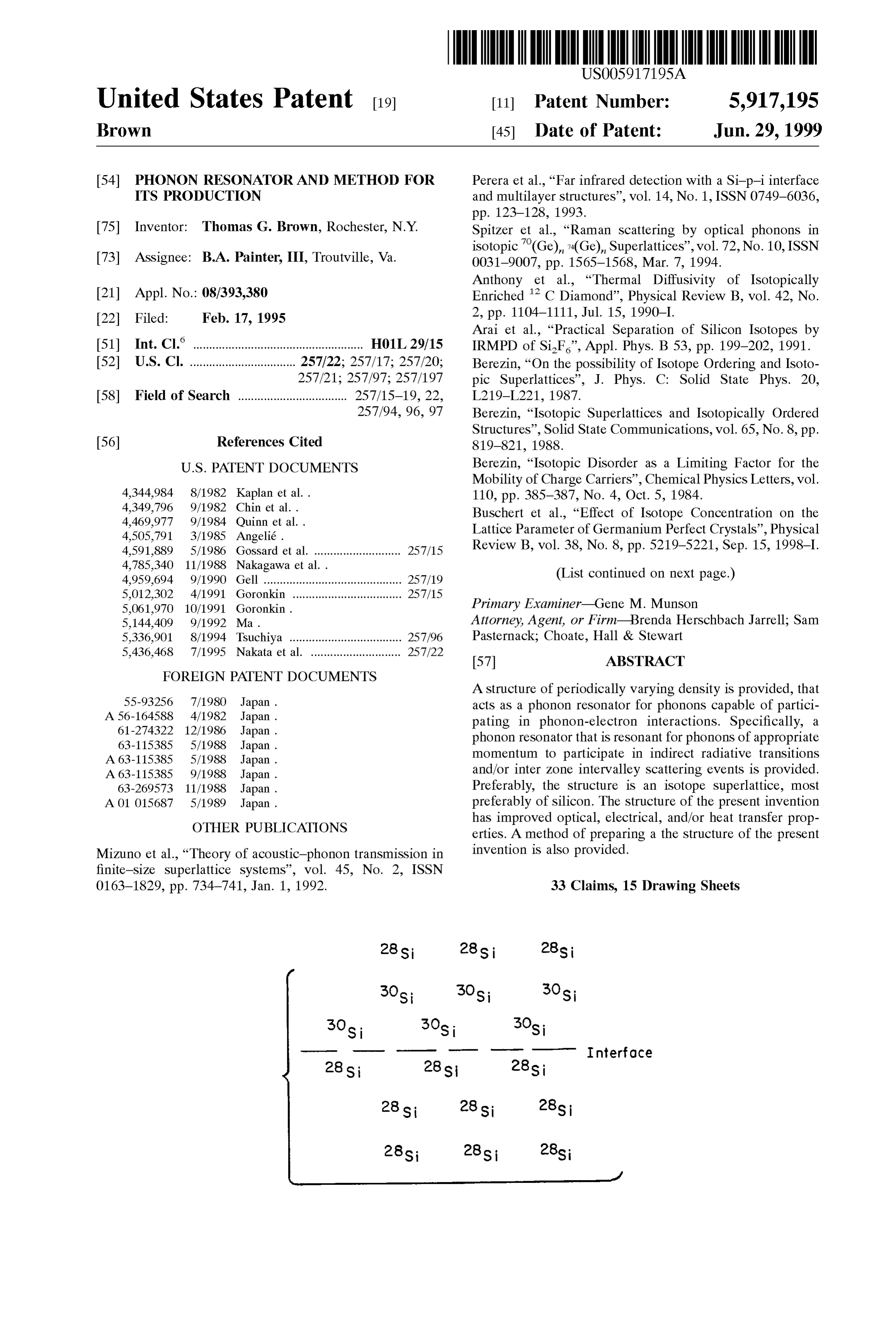
Interface
Page 2
OTHER PUBLICATIONS Iyer et al., “Light Emission from Silicon', Science, vol. 260,
Clark et al., “Silane Purification Via Laser-induced Chem istry”, Appl. Phys. Lett, 32(1), pp. 46–49, Jan. 1, 1978. Kamioka et al., “Isotope-Selective Infrared Multiple Photon Cohen, “Band Structures and Pseudopotential Form Factors Decomposition of Hexafluorodisilane”, J. Phys. Chem., 90, for Fourteen Semiconductors of the Diamond and pp. 5727–5730, 1986.
Zinc-blende Structure”, Physical Review, vol. 141, No. 2, Klein, “Phonons in Semiconductor Superlattices”, IEEE pp. 789–796, Jan. 1966. Journal of Quantum Electronics, vol. QE-22, No. 9, pp. Collins et al., “Indirect Energy Gap of "C Diamond", vol. 1760–1770, Sep. 9, 1986.
65, No. 7, pp. 891-894. Aug. 13, 1990. Koblinger et al., “Phonon Stop Bands in Amorphous Super Döhler et al., Doping Superlattices (“n-i-p-i Crystals”), lattices”, Physical Review B, vol. 35, No. 17, pp. Journal of Quantum Electronics, vol. QE-22, No. 9, pp. 9372-9375, Jun. 125, 1987-I.
Egami et al., “Lattice Effect of Strong Electron Correlation: Liu et al., “A RHEED Study of the Surface Reconstructions Implication for Ferroelectricity and Superconductivity”, of Si(001) During Gas Source MBE Using Disilane”, Sur Science, vol. 261, pp. 1307–1310, Sep. 3, 1993. face Science 264, pp. 301–311, 1992. Epling et al., “Isotope Enrichment by Photolysis on Ordered Lyman et al., “Enrichment of Boron, Carbon, and Silicon Surfaces”, J. Am. Chem. Soc. 1981, 103, pp. 1238-1240, Isotopes by Multiple-Photon Absorption of 10.6lim Laser 1981. Radiation”, Journal of Applied Physics, vol. 47, No. 2, pp. Esaki et al., “A Bird's-Eye View on the Evolution of 595-601, Feb. 1976.
Semiconductor Superlattices and Quantum Wells”, Journal Nieminen, “Hydrogen Atoms Bond Together', Nature, vol. of Quantum Electronics, vol. QE-22, No. 9, pp. 1611-1624, 356, pp. 289–290, Mar. 26, 1992.
Etchegoin et al. “Phonons in isotopically disorded Ge” Nilsson et al., “Study of the Homology between Silicon and Physical Review B, vol. 48, No. 17, Nov. 1, 1993–I. Germanium by Thermal-Neutron Spectrometry”, Physical Fuchs et al., “Anharmonic Decay Time, Isotopic Scattering Review B, vol. 6, No. 10, Nov. 15, 1972. Time, and Inhomogeneous Line Broadening of Optical Olander, “The Gas Centrifuge”, Scientific American, vol. phonons in 'Ge, 'Ge, and natural Ge Crystals", Physical 239, No. 2, pp. 37-43, Aug. 1978. Review B, vol. 44, pp. 8633–8642, No. 16, Oct. 15, 1991-II. Presting et al., “Ultrathin SiGe Strained Layer Superlat Fuchs et al., “Infrared Absorption in Ge and Natural Ge tices-a Step Towards Si Optoelectronics', Semicond. Sci. Crystals: Effects of Isotopic Disorder on q=o Phonons”,
Physical Review B, vol. 45, pp. 4065–4070, No. 8, Feb. 15, Technol. 7, pp. 1127-1148, 1992. 1992-II. Sedgwick et al., “Atmospheric Pressure Chemical Vapor Fuchs et al., “Isotopic Ge Superlattices: Vibrational Prop Deposition of Si and SiGe at Low Temperatures”, J. Vac. erties”, Superlattices and Microstructures, Vol. 13, No. 4, pp. Sci. Technol. A 10(4), pp. 1913–1919, Jul/Aug. 1992. 447-4581993. Spitzer et al., Raman Scattering by Optical Phonons in Haller, “Semiconductor Isotope Engineering, LBL-34279, Isotopic (Ge), (Ge), Superlattices, Physical Review Preprint. Proc. GADEST 93, Gettering and Defect Engi Letters, vol. 72, pp. 1565–1568, No. 10, Mar. 7, 1994. neering in Semiconductors, Klingemihle, Germany, Oct.
9-14, 1993. Wilkinson et al., “Infrared Spectra of Some MH, Mol Hass et al., “Effects of Isotopic Disorder on the Phonon ecules”, The Journal of Chemical Physics, vol. 44, No. 10, Spectrum of Diamond”, Physical Review B, vol. 44, pp. pp. 3867–3871, May 15, 1966.
12046–12176, No. 21, Dec. 1, 1991-I. Zollner et al., “Isotope and Temperature Shifts of Direct and Itoh et al., “High Purity Isotopically Enriched ' Ge and 7" Indirect Band Gaps in Diamond-Type Semiconductors”, Ge Single crystals: Isotope Separation, Growth, and Prop Physical Review B, vol. 45, No. 7, pp. 3376-3385, Feb. 15, erties”, vol. 8, No. 6, Jun. 1993. 1992-I.
Page 3
Drawing sheet — no readable text.
Page 4
Drawing sheet — no readable text.
Page 5
Drawing sheet — no readable text.
Page 6
Drawing sheet — no readable text.
Page 7
Drawing sheet — no readable text.
Page 8
fight
Emission
t Light
Emission
EH - Higher
RegionBandgap
86 Electron & Holes t Confined Here
Region of 84 Higher Bandgap
Region of High
Refractive . 95 Index n, 100 Waveguide
Page 9
Drawing sheet — no readable text.
Page 10
Drawing sheet — no readable text.
Page 11
Drawing sheet — no readable text.
Page 12
Drawing sheet — no readable text.
Page 13
Drawing sheet — no readable text.
Page 14
Drawing sheet — no readable text.
Page 15
Drawing sheet — no readable text.
Page 16
Drawing sheet — no readable text.
Page 17
Drawing sheet — no readable text.
Page 18
PHONON RESONATOR AND METHOD FOR In addition, LEDs have been fabricated using silicon ITS PRODUCTION carbide. However, it has not been possible to produce optical BACKGROUND OF THE INVENTION amplifiers (e.g. lasers) using indirect bandgap materials for Semiconducting materials have proven to be the corner a discussion of the underlying reasons. Stone of the electronics revolution; and Silicon, thanks to its Thus, there is a need for development of materials with purity, ease of fabrication, and high yield in manufacturing, improved optical, electronic, and/or heat dissipation prop has been the dominant material utilized in integrated circuit erties. There is a particular need for improved Semiconduc technology. With the constant pressure for faster, more tor materials. Preferably, the improved materials should be efficient devices, there is much interest in developing or compatible with present-day electronic materials (e.g. identifying new, low-cost materials that can meet the inter Silicon).
connect demands associated with increasing parallelism and SUMMARY OF THE INVENTION higher data rates. Additionally, pressure to reduce device
Size and density has focused efforts on identifying materials The present invention provides an improved material in with improved heat dissipation and/or electrical conductiv 15 which optical, electronic, and/or heat dissipation character ity characteristics. istics are modified because certain electron-phonon interac The use of Superconducting materials, in combination tions are enhanced or Suppressed in the material. with established Semiconductor technologies, has been pro Specifically, the present invention provides an indirect band posed as a Solution to the heat dissipation problems encoun gap material that functions as a resonator for phonons of tered with present-day Semiconducting materials. desired wavenumbers. In Some embodiments, the phonon Specifically, it has been Suggested that Superconducting resonator of the present invention displays increased photon wires and junctions could be used in integrated circuits to emission or absorption capability relative to known indirect reduce heat dissipation. Unfortunately, even recently bandgap materials. In other embodiments, the present discovered “high temperature” Superconductors do not oper phonon resonator has enhanced electrical properties, Such as ate above cryogenic temperatures. Moreover, the expense 25 electrical conductivity. The phonon resonator of the present and engineering difficulty associated with integration of invention can also show improved thermal conductivity available Superconducting and Semiconducting technologies characteristics, and can be incorporated into electronic make this possibility impractical, if not infeasible. devices to provide improved heat transfer. The present Optical communication Systems offer a potential Solution invention also provides an isotope Superlattice that is a to the interconnect problem, but development efforts have phonon resonator.
been hampered by the difficulties associated with integrating The phonon resonator of the present invention can be efficient light Sources into available Silicon circuits. Silicon incorporated into any of a variety of different optical devices itself, like the other members of its periodic-table family Such as, for example, LEDs and lasers. The present phonon (group IV), has limited optical capabilities due to its cen resonator can be utilized, for example, in optical trosymmetric crystal Structure and an indirect band gap, 35 communications, data Storage, printing, uV-light emission, which prohibits photon emission via efficient, band-to-band infrared lasers, etc. Other embodiments of the phonon radiative transmission (see below). resonator of the present invention have enhanced electrical Much effort has been directed at circumventing the selec conductivity
Such as, for and can be utilized in electrical applications example, Superconducting applications.
tion rules that forbid band-to-band radiative transmission in indirect bandgap Semiconductors, in order to develop Semi 40 The present invention also provides methods of fabricat conducting materials with improved optical properties (Iyer ing an isotope Superlattice that is a phonon resonator. et al. Science 260:40-46, 1993). One approach has been to In Some embodiments, the phonon resonator of the introduce Suitable impurities into the group IV lattice. Tight present invention is a structure of Substantially periodically binding of an exciton (an electron-hole pair) to an impurity varying density, which Structure comprises at least one first can provide efficient radiative transmissions if a Sufficient 45 region of a first density; and at least one Second region of a Volume of impurities has been introduced. The most Suc Second density, the first and Second regions being adjacent cessful of these efforts have involved isoelectronic com one another and alternating in the Structure So that the plexes and the rare-earth dopant Erbium. However, Erbium, Structure has a Substantially periodically varying density. like other radiative impurity complexes, is difficult to intro The period of the structure is selected such that the structure duce in a concentration Sufficient to provide optical gain. 50 is Substantially resonant for phonons of appropriate Efforts have also been directed at growing ordered alloys wavevector to participate in electron-phonon interactions and Superlattices, with the idea of using band gap engineer (e.g. phonons of appropriate wavevector to participate in ing to “fold' the Brillouin Zone and achieve a quasi direct radiative electronic transitions, phonons of appropriate gap material (Presting et al. Semicond. Sci. Technol. wavevector to participate in interZone and/or intervalley 7:1127-1148, 1992). The most popular of these materials 55 Scattering of conduction band electrons). Systems has been Silicon-germanium, with Some recent In other embodiments, the phonon resonator of the interest in the quaternary alloy carbon-Silicon-germanium present invention is a Structure having degenerate conduc tin. These materials have yet to show the radiative efficiencytion band Valleys and Substantially periodic variations in found in direct bandgap materials. material composition So that Scattering of electrons between A widely studied (but poorly understood) mechanism for 60 the degenerate conduction band Valleys is enhanced relative light emission occurs in Silicon that has undergone an to intervalley electron Scattering in a structure that lacks the electrochemical etching process (Iyer et al. Supra). The etch Substantially periodic variations. produces a porous Structure with nanometer-size particles In Some embodiments, the density or material composi that, upon passivation, provides efficient, Visible photolumi tion of the Structure varies periodically in more than one neScence. Samples of etched Silicon have also been excited 65 dimension; in other embodiments, each region comprises a in electroluminescence, and have attracted Some interest for layer, So that the density or material composition of the display devices. Structure varies periodically in only one dimension.
Page 19
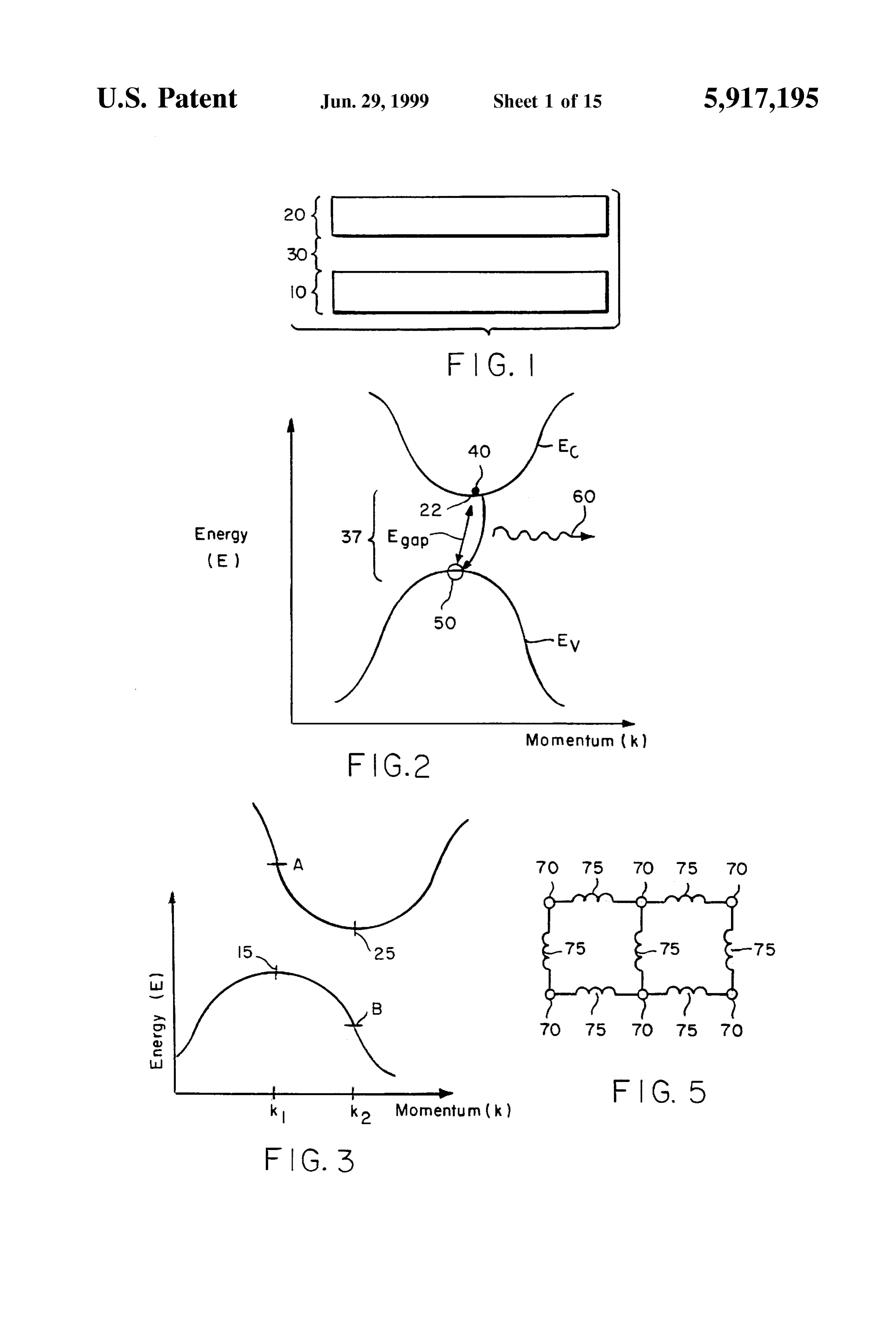
In preferred embodiments of the present invention, the isotope Superlattice is preferably performed by a method phonon resonator is a layered Structure comprising an iso Selected from the group consisting of chemical vapor tope Superlattice in which each layer is enriched for one deposition, molecular beam epitaxy, and chemical beam isotope of an element. Most preferably, the layers are epitaxy. In Some embodiments, the Steps of Separating and enriched for different isotopes of the same element, prefer assembling are performed separately. In alternate ably Silicon. In Some preferred embodiments of a Silicon embodiments, the Steps of Separating and assembling are isotope Superlattice of the present invention, the Superlattice performed Simultaneously. In preferred embodiments, an has a period that is an integer multiple of five atomic layers, isotope Superlattice of the present invention is produced in alternate preferred embodiments, the period is an integer using laser-assisted chemical vapor deposition. multiple of ten atomic layers. DESCRIPTION OF THE PREFERRED The phonon resonator of the present invention, in Some EMBODIMENTS embodiments, is also resonant for (directional or coherent) Drawings phonons that are generated by Stimulated phonon emission, FIG. 1 is a Schematic diagram of the energy bands in a So that the resonator provides accelerated heat transfer. In Solid.
Some embodiments, the phonon resonator provides a Sto 15 FIG. 2 is an energy VS. momentum diagram for a direct chastic phonon resonance. bandgap material.
The present invention also provides various devices incor FIG. 3 is an energy VS. momentum diagram for an indirect porating a phonon resonator. The invention provides, among bandgap material.
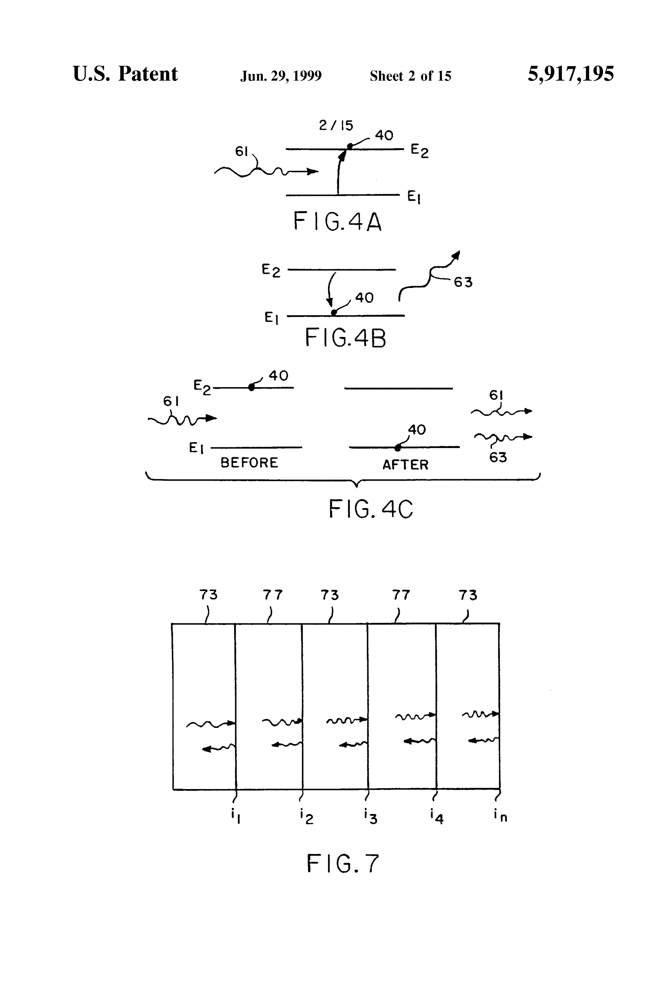
other things, a light-emitting device, comprising a phonon FIG. 4 illustrates the three possible photon-electron inter resonator, a first electrode disposed on a first Side of the actions. Specifically, FIG. 4A illustrates absorption of a Structure; and a Second electrode disposed on a Second Side photon by an electron that can occupy one of only two of the Structure, the Second Side being opposite the first Side. energy States, FIG. 4B illustrates Spontaneous emission of a At least one of the electrodes can be transparent if desired. photon by an electron that can occupy one of only two The light-emitting device of the present invention can energy States, and FIG. 4C illustrates Stimulated emission of include a p-doped region and an n-doped region, and may 25 a photon by an electron that can occupy one of only two function as a light-emitting diode (LED). The p- and energy States.
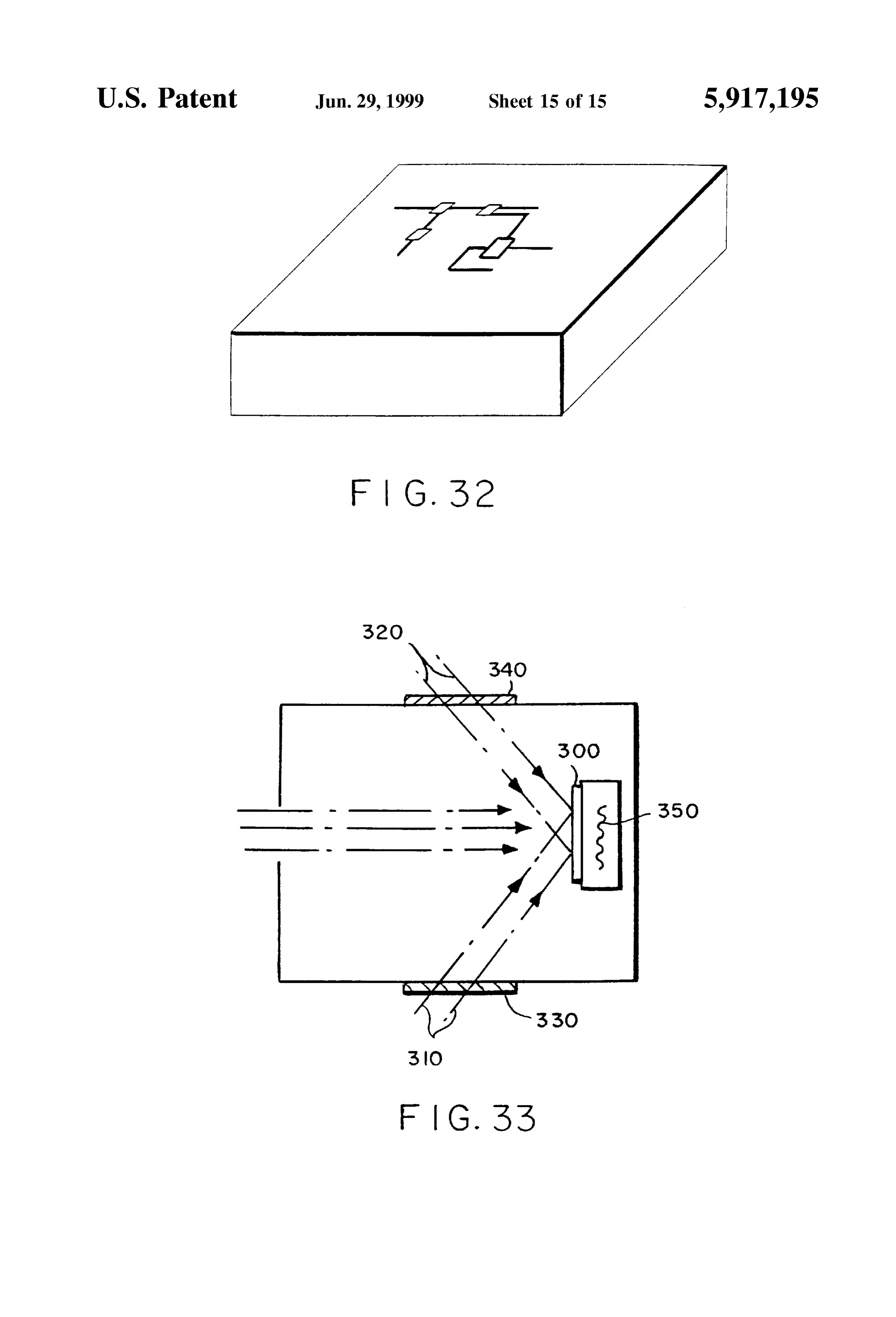
n-doped regions of the light-emitting device of the present FIG. 5 is a Schematic diagram of atoms arranged in a invention may have a higher bandgap than does the phonon crystalline Solid.
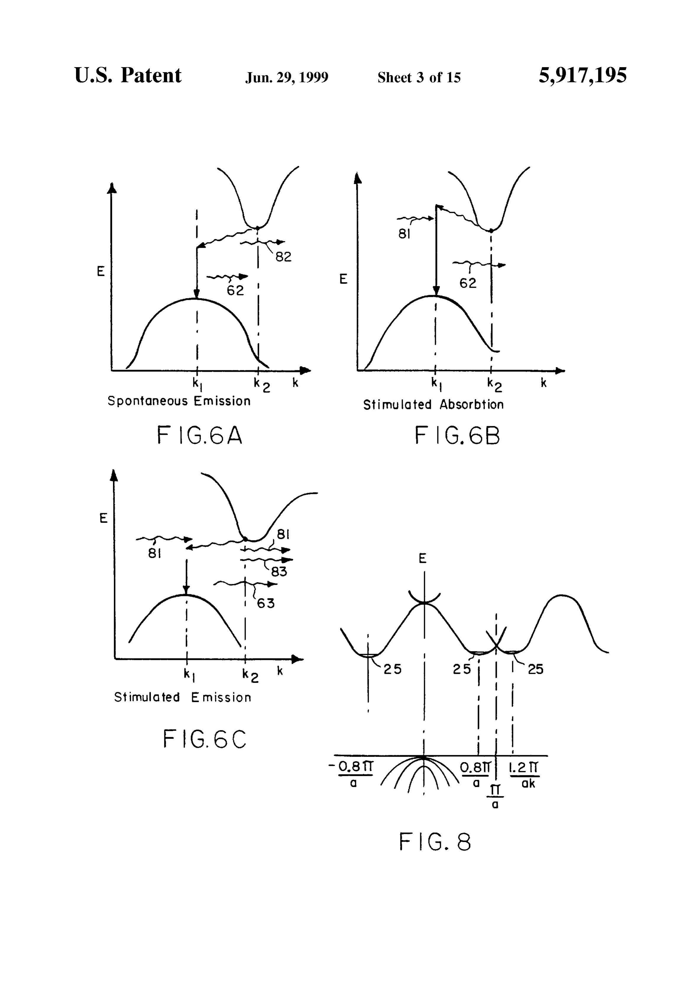
resonator, So that electrons and holes are confmed within the FIG. 6 depicts phonon-assisted radiative transitions in an phonon resonator. The light-emitting device of the present indirect bandgap material. FIG. 6A illustrates Spontaneous invention preferably includes a dielectric waveguide, most emission of a phonon as a result of an electron-phonon preferably formed by the p-doped region and the n-doped interaction that stimulates photon emission; FIG. 6B illus region, each having a refractive index higher than that of the trates Stimulated phonon absorption; and FIG. 6C illustrates Structure. In Some embodiments, the light-emitting device of Stimulated phonon emission.
the present invention is a laser (e.g. a cleaved facet 35 FIG. 7 is a schematic design of a distributed feedback reflection, distributed feedback, and/or vertical cavity Sur laser.
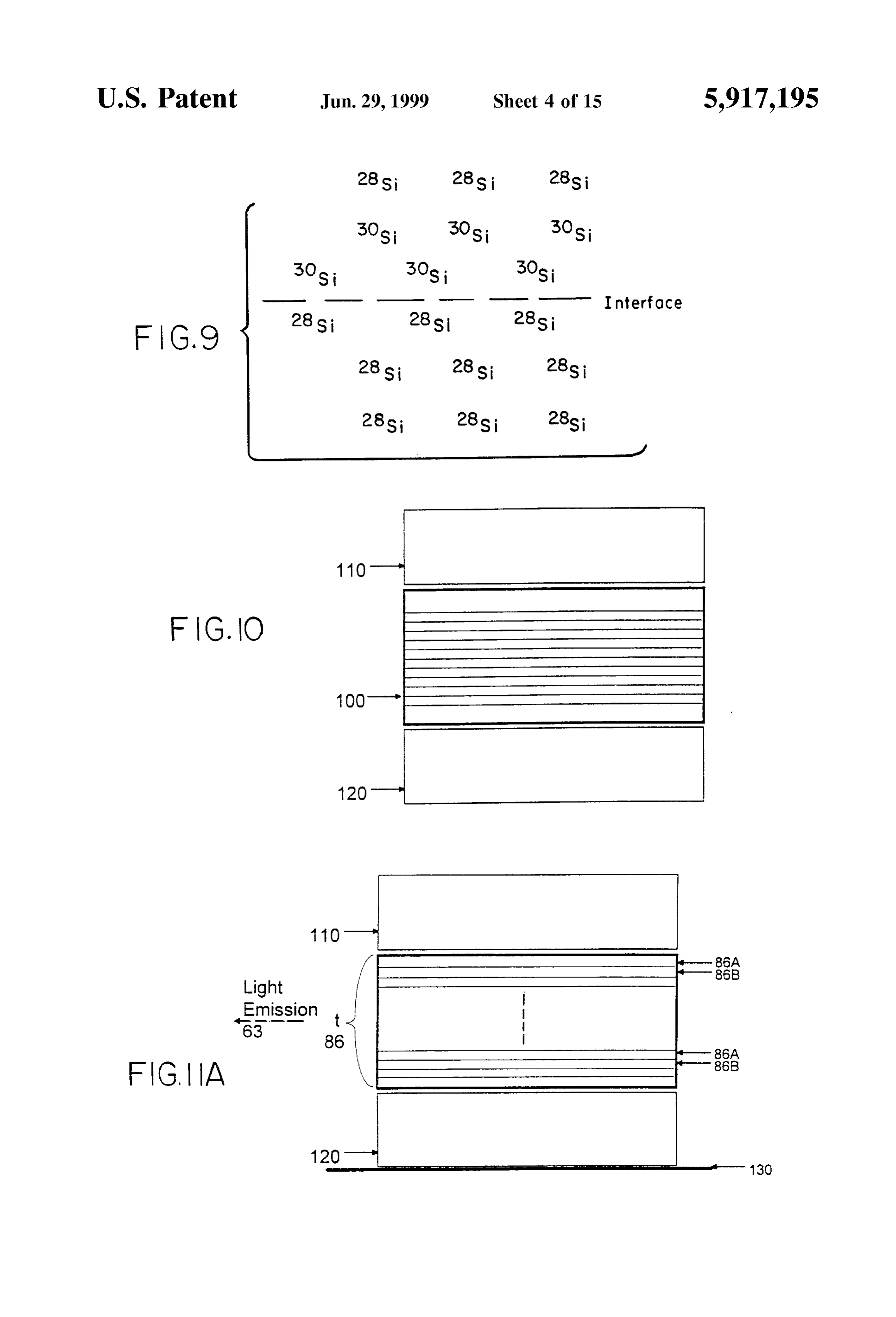
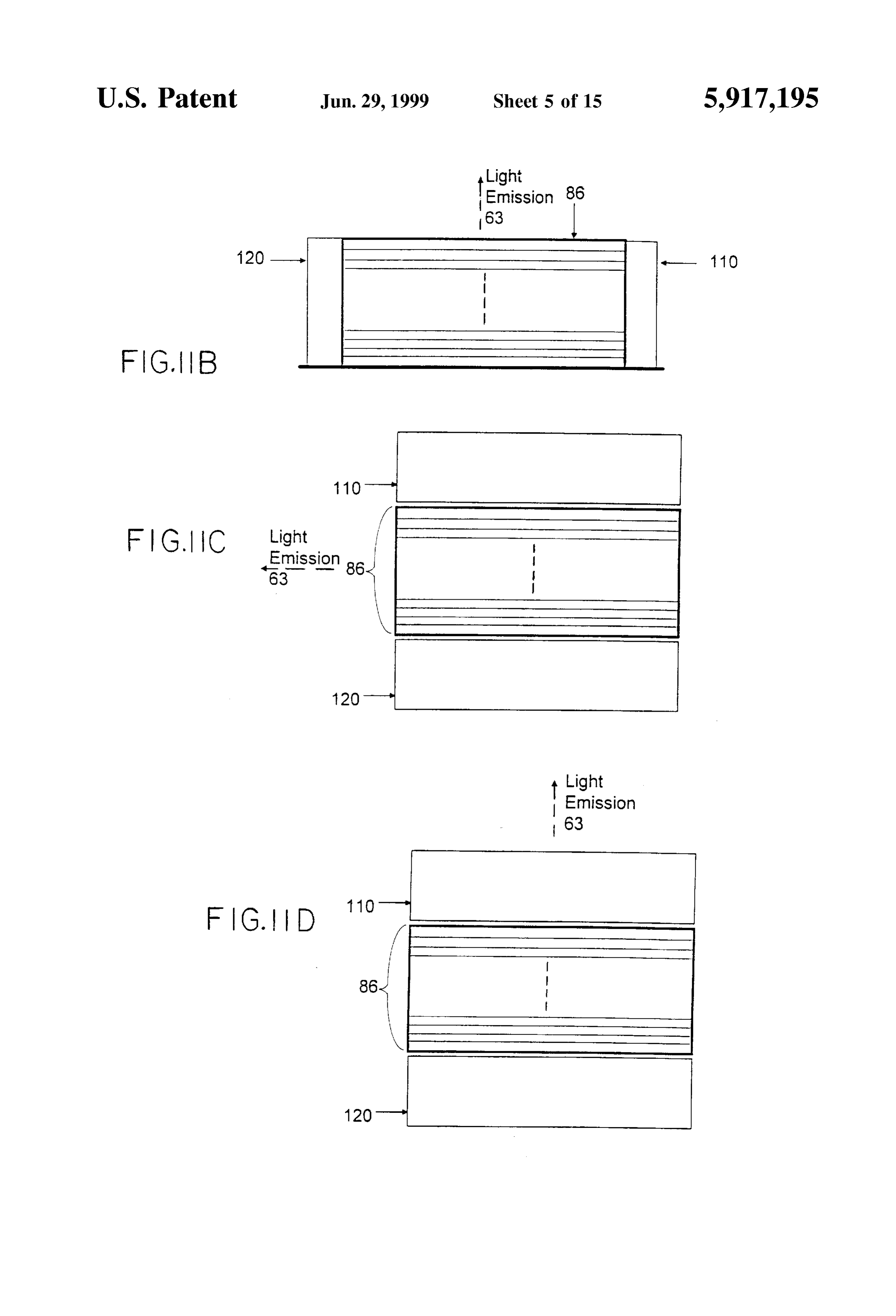
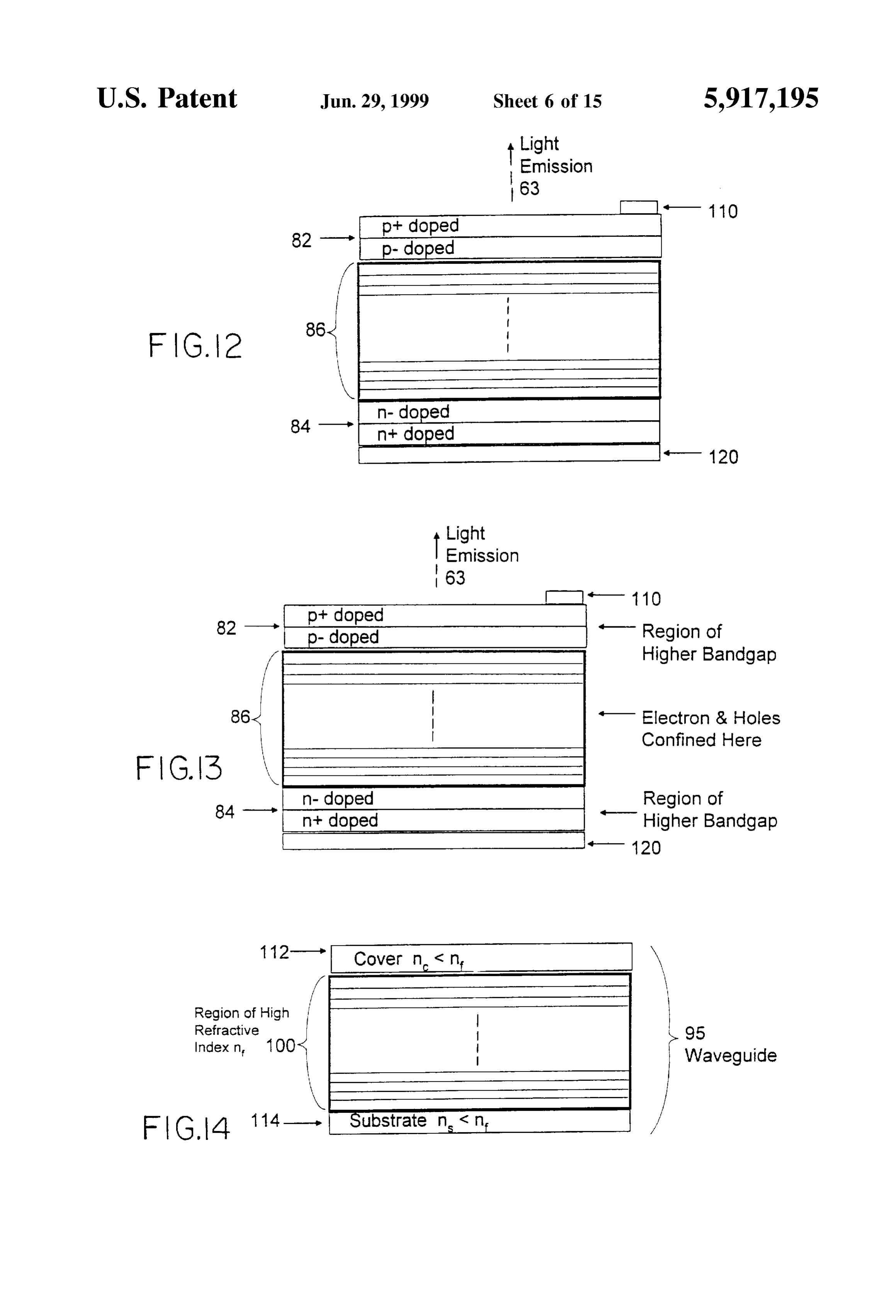
face emitting). FIG. 8 is an energy VS. momentum diagram for Silicon. The present invention also provides devices Selected from FIG. 9 shows a schematic diagram of a portion of a silicon the group consisting of light emitting devices, light emitting isotope Superlattice of the present invention. diodes, laser diodes, cleaved facet reflection lasers, distrib 40 FIG. 10 illustrates a light emitting device that utilizes a uted feedback lasers, Vertical cavity Surface emitting lasers, phonon resonator of the present invention. optical detectors, optical modulators, non-linear optical FIG. 11 presents four embodiments (as FIGS. 11A, 11B, devices, electrical conductors, planar transformers, diodes, 11C, and 11D) of a light-emitting device of the present bipolar transistors, field-effect transistors, integrated invention.
circuits, SQUIDS, Josephson junctions, transducers, and 45 FIG. 12 depicts a light-emitting diode (LED) of the microwave detectors, that are improved over conventional present invention.
devices because they incorporate a phonon resonator that is FIG. 13 depicts an LED of the present invention in which Substantially resonant for phonons of appropriate wavevec carrier confinement is achieved by means of a heterojunc tor to participate in phonon-electron interactions. tion.
The present invention also provides a method for produc 50 FIG. 14 depicts and edge-emitting LED of the present ing a phonon resonator comprising the Step of producing a invention.
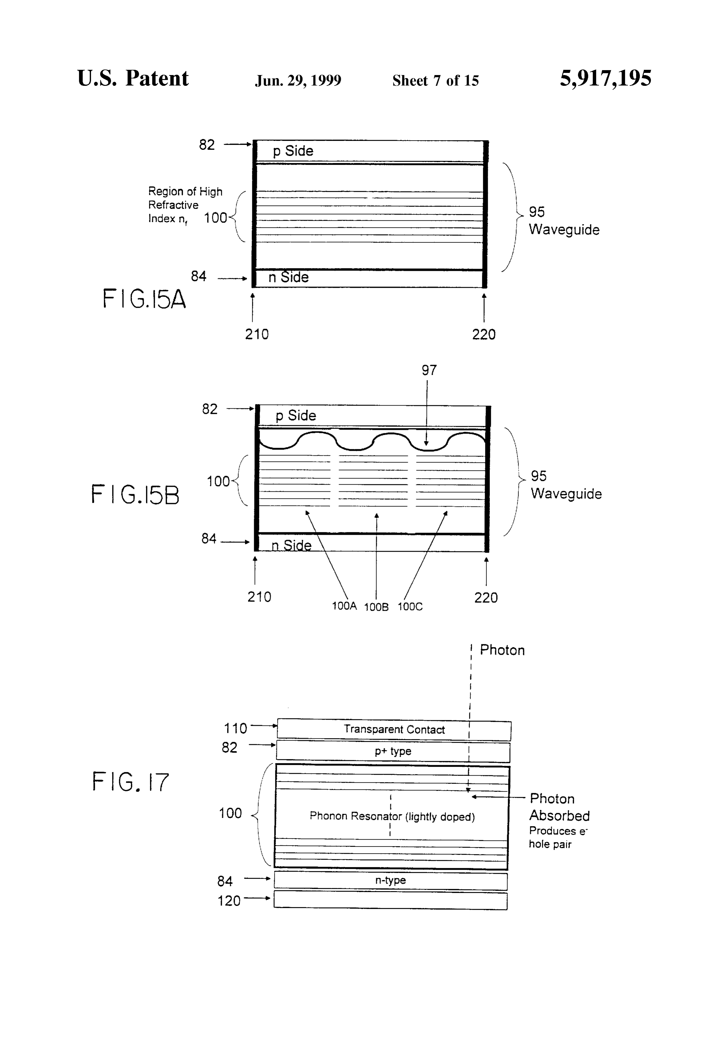
Structure of Substantially periodically varying density com FIG. 15 presents two embodiments (as FIGS. 15A and prising at least one first region or layer of a first density; and 15B) of a laser diode of the present invention. FIG. 15A at least one region or Second layer of a Second density, the depicts a cleaved facet reflection laser. FIG. 15B depicts a first and Second regions or layers being adjacent one another 55 distributed feedback laser.
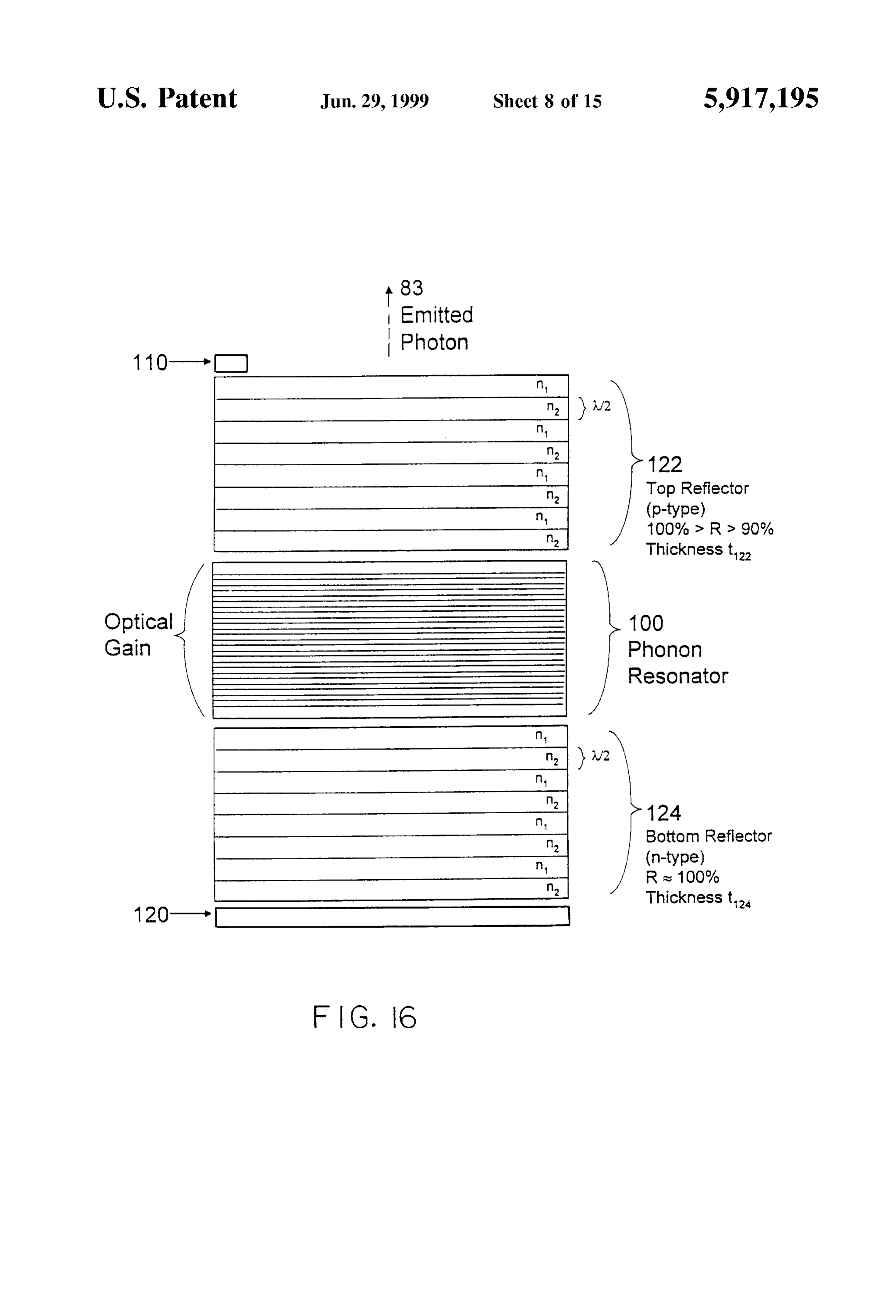
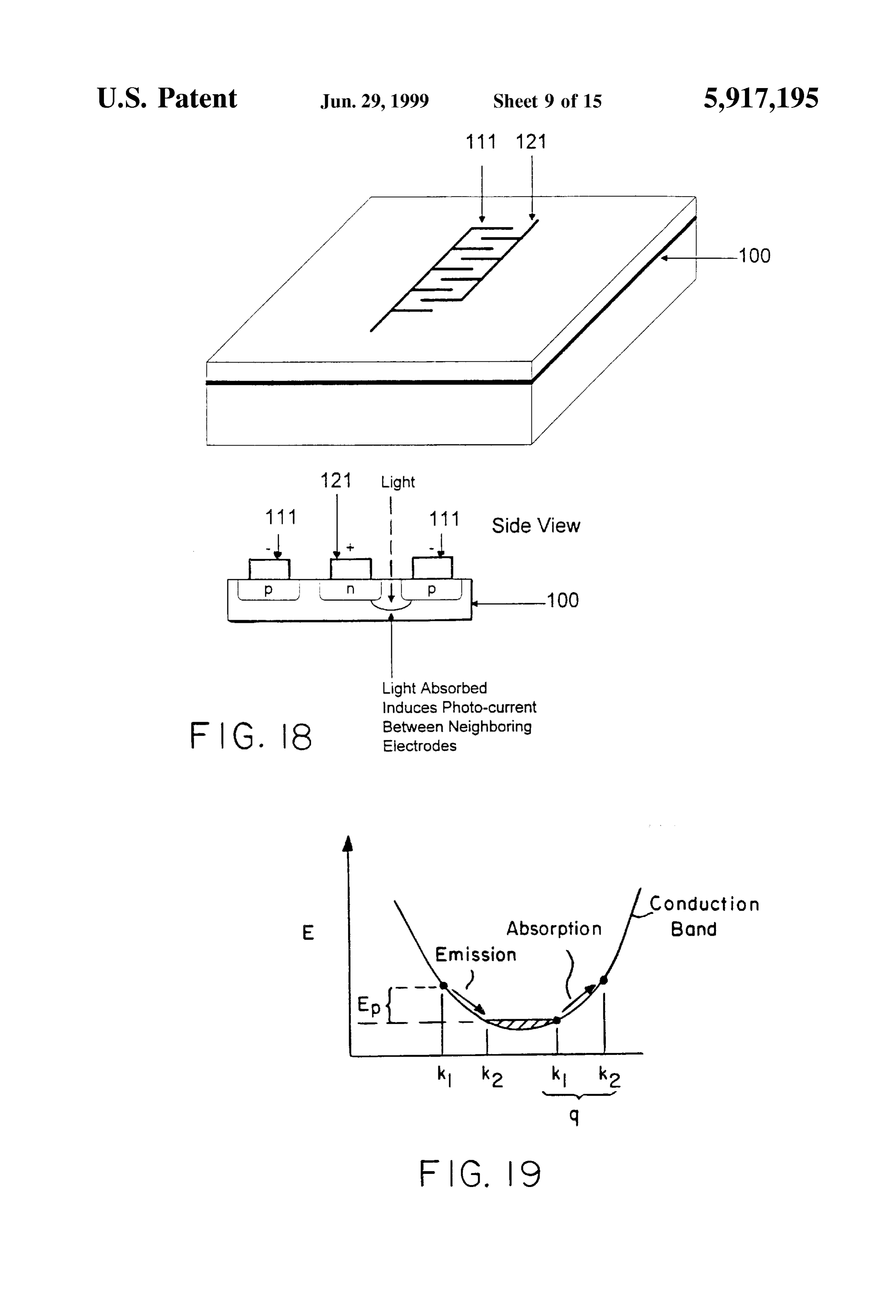
and alternating in the Structure So that the Structure has a FIG. 16 depicts a Vertical Cavity Surface Emitting Laser Substantially periodically varying density, the period of the (VECSEL) of the present invention. Structure being Selected Such that the Structure is Substan FIGS. 17 and 18 depict alternate embodiments of an tially resonant for phonons of appropriate wavevector to optical photodetector incorporating a phonon resonator of participate in electron-phonon interactions. In preferred 60 the present invention.
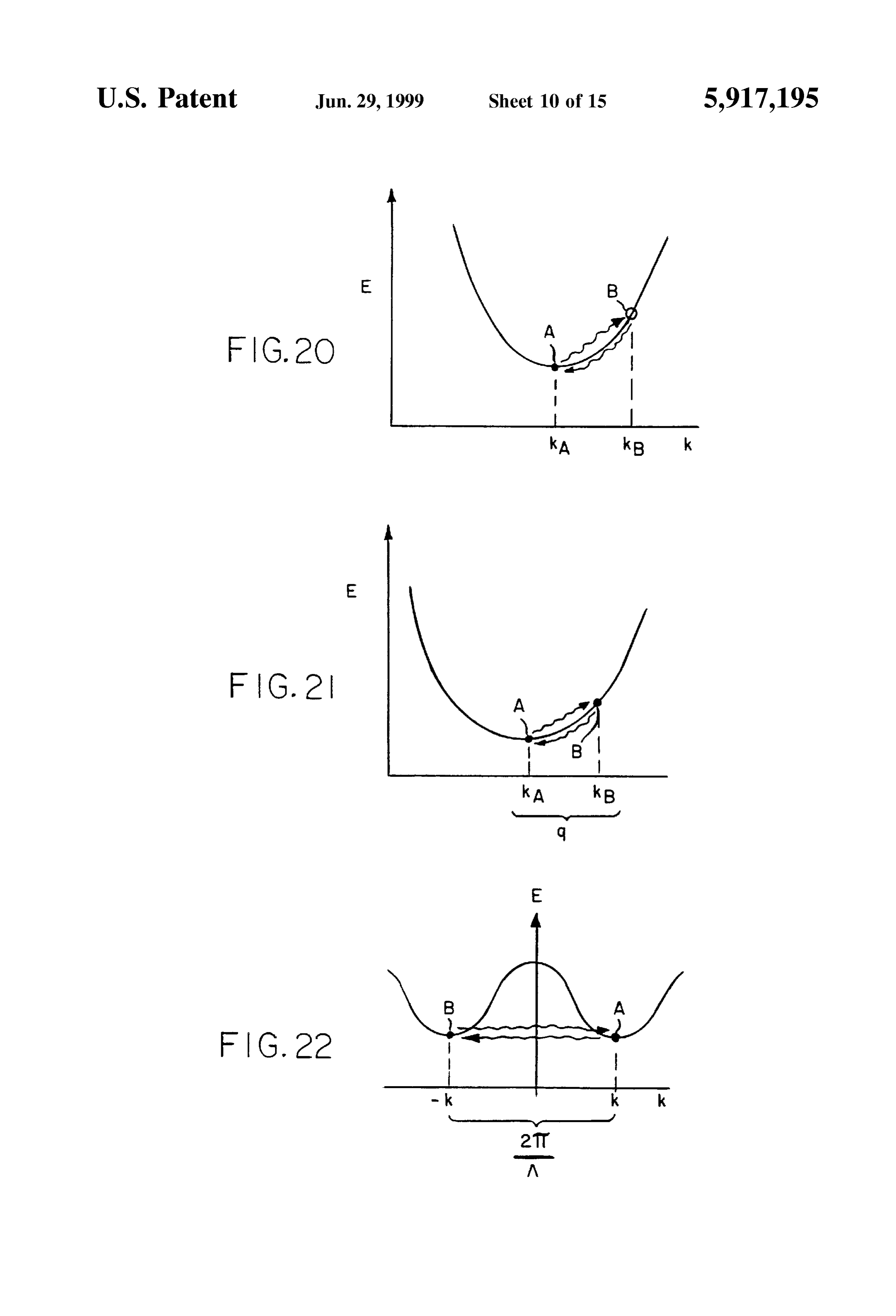
embodiments, the method of the present invention involves FIG. 19 depicts absorption and emission of a phonon by producing an isotope Superlattice by Separating isotopes, and a conduction-band electron in a Semiconductor material. assembling the Superlattice. According to the present FIG. 20 depicts coherent absorption and emission of a invention, isotope Separation is preferably performed by a phonon by a conduction-band electron in a Semiconductor method Selected from the group consisting of distillation, 65 material.
extraction, centrifugation, diffusion, electrochemical FIG. 21 illustrates phonon-mediated exchange between methods, and electromagnetic methods, assembly of an two conduction-band electrons in a Semiconductor Solid.
Page 20
S 6
FIG. 22 illustrates phonon-mediated exchange between which the phonon resonator affects the optical, electronic, electrons in different, degenerate conduction band minima in and/or heat transfer properties of the material from which a single conduction band of a Semiconductor material. the resonator is constructed.
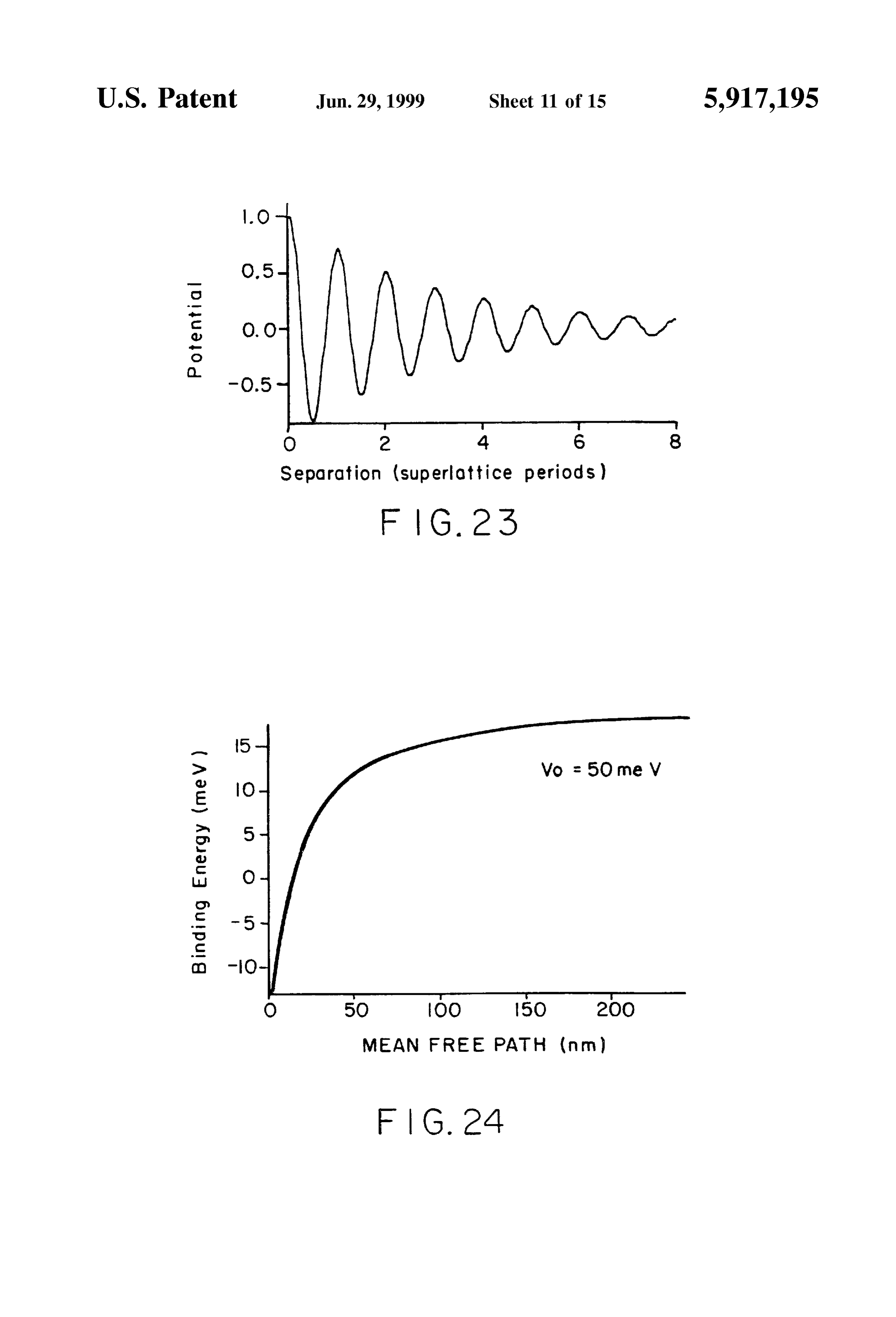
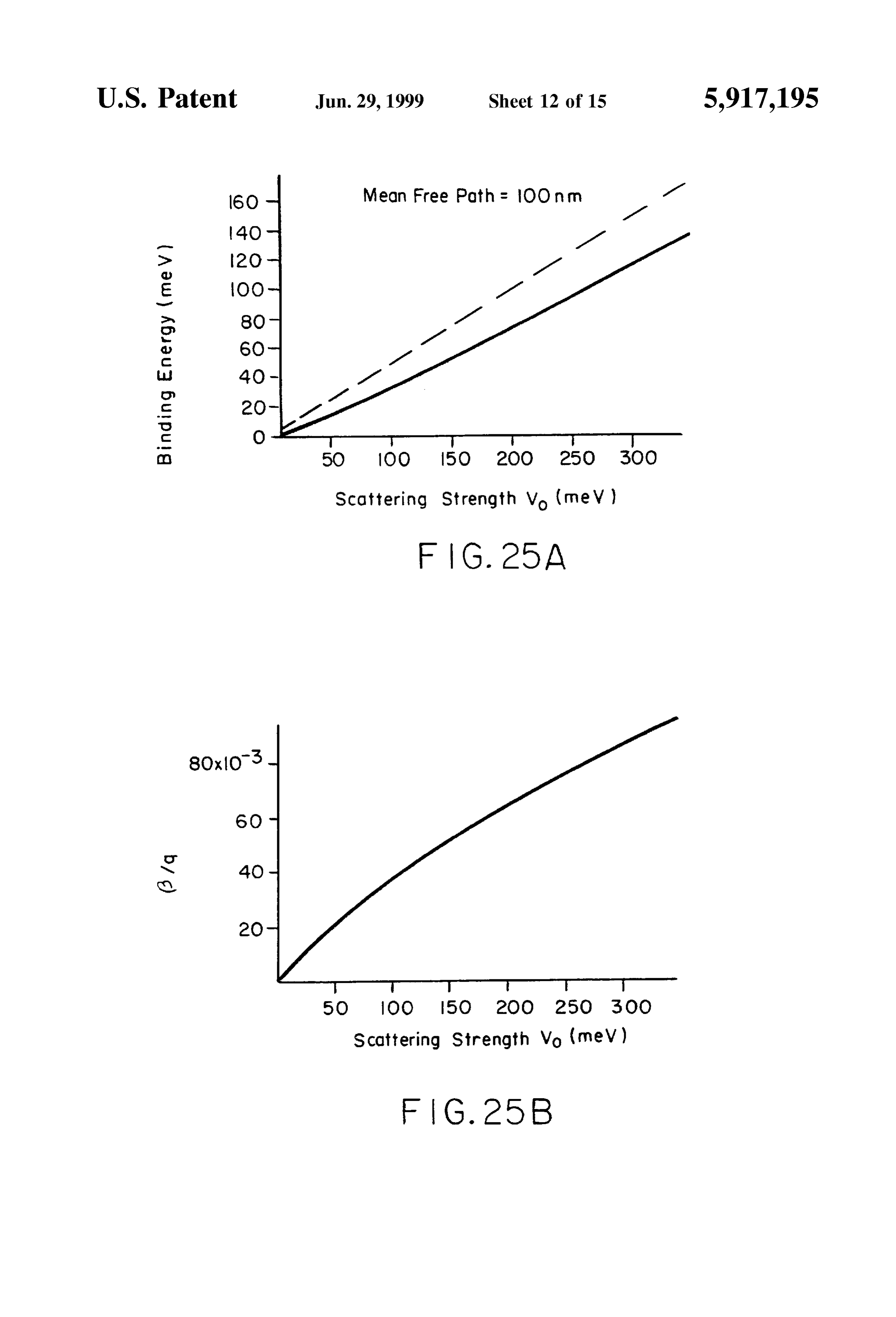
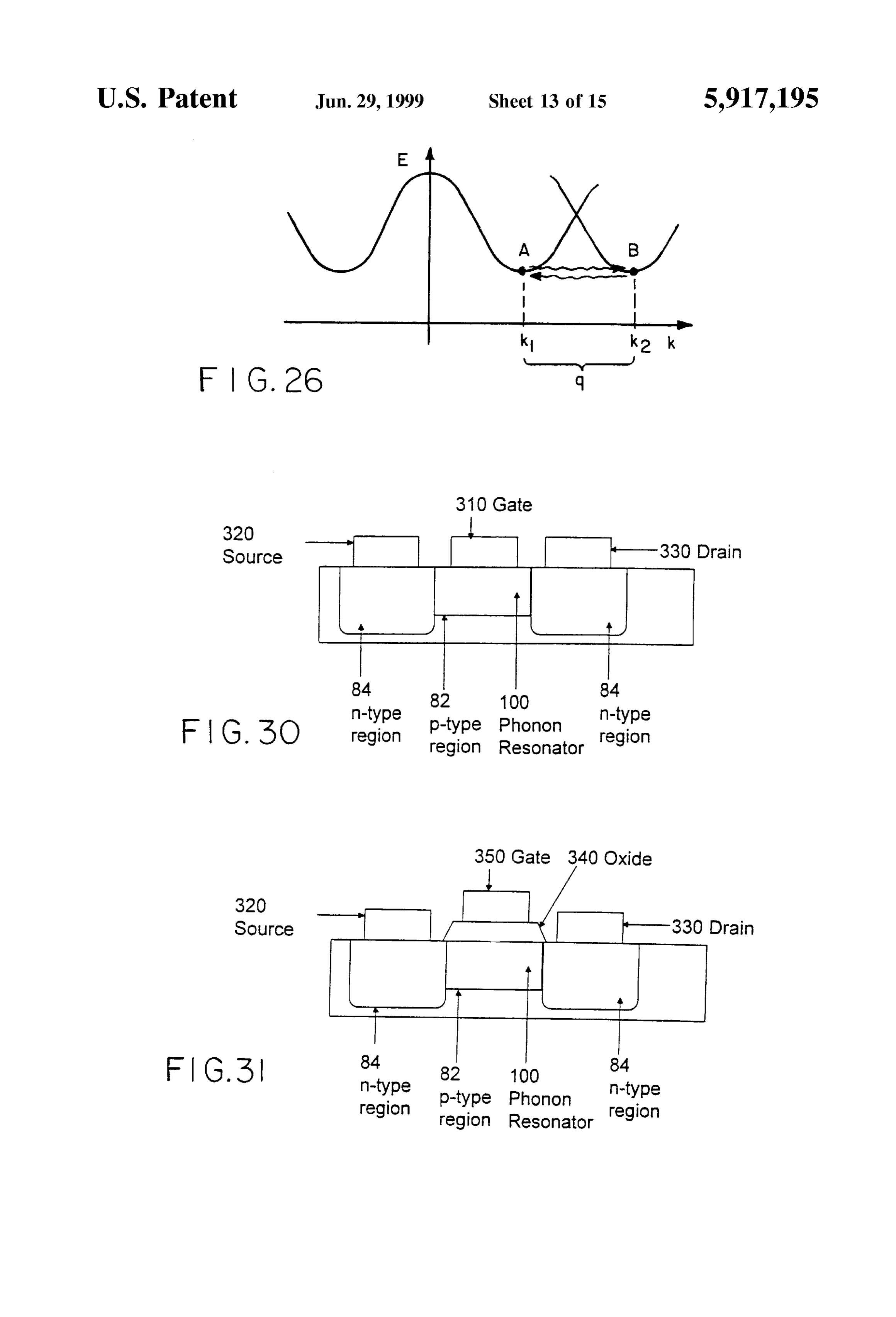
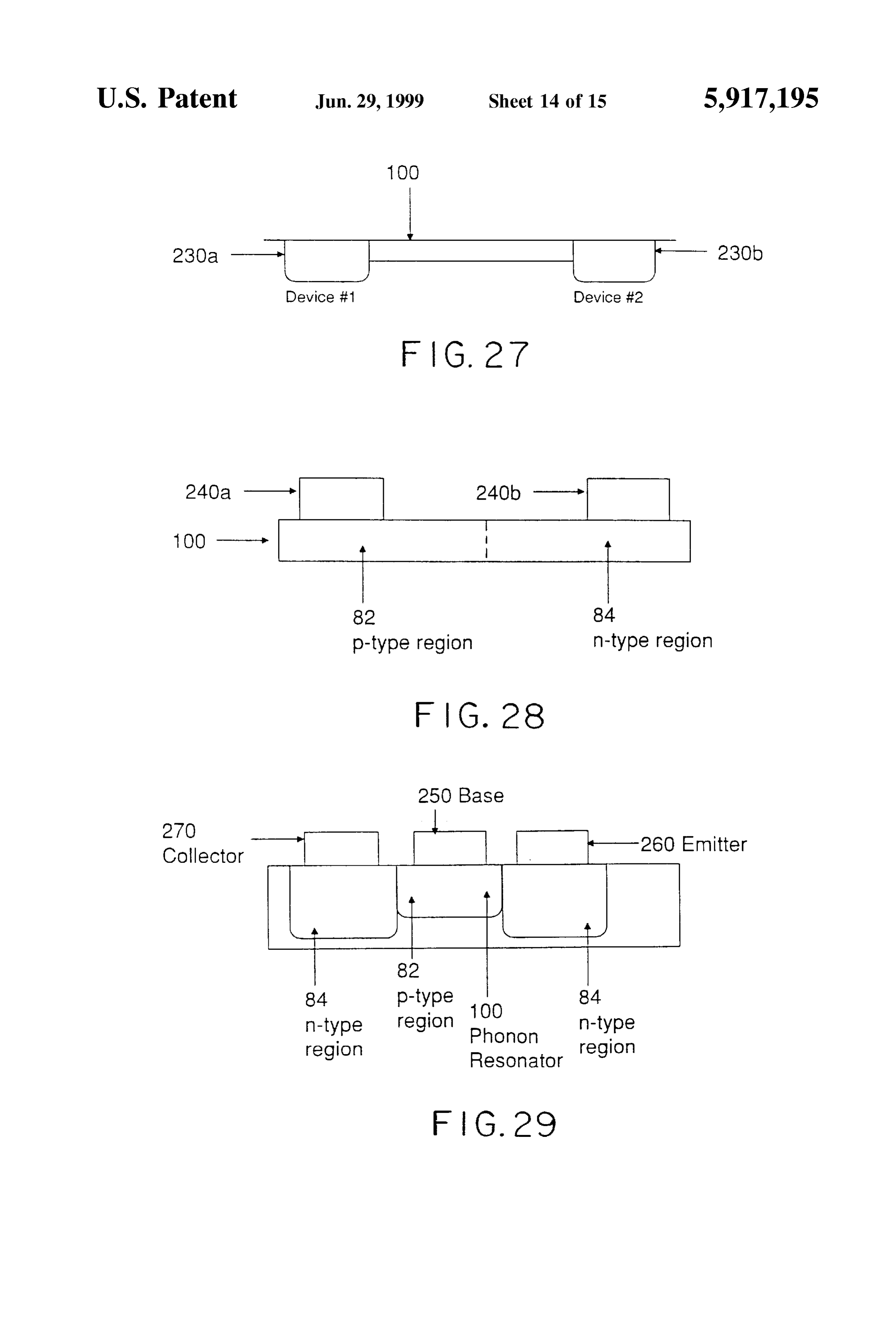
FIG. 23 presents a graph of the normalized electron pair Enhancement of Optical Properties potential as a function of the pair Separation, measured in The present invention encompasses indirect bandgap Superlattice periods. For the calculation presented, the mean materials having enhanced optical properties. In order that free path is 5 Superlattice periods. certain aspects and advantages of the present invention will FIG. 24 is a graph showing the reduction in electron pair be more readily appreciated, we begin with a discussion of binding energy that occurs with decreasing electron mean the properties of indirect bandgap Semiconductor materials, free path. as opposed to direct bandgap materials. FIG. 25 shows the electron pair binding energy as a First of all, we point out that, in any Semiconductor Solid function of the Scattering potential for a fixed mean free (i.e. whether a direct or indirect bandgap material) that is path. free of defects and impurities, electrons can acquire only FIG. 26 depicts intervalley scattering of electrons in particular energy values that are within two discrete bands: conduction band minima of neighboring Brillouin Zones. 15 a “valence band', which encompasses the range of energies FIG.27 shows a low-resistance electrical conductor of the possessed by electrons in bound energy States, and a “con present invention. duction band', which corresponds to the allowable energy FIG. 28 depicts an electrical diode of the present inven States of free electrons or electrons that are unbound and tion. move about the crystal lattice of the solid. FIG. 1 presents a FIG. 29 depicts a bipolar transistor of the present inven Schematic representation of a Valence band 10 and a con tion. duction band 20, separated by an “energy bandgap' 30 that FIG. 30 depicts an n-type Junction Field Effect Transistor corresponds to the range of impermissible energies between (JFET) of the present invention. the valence 10 and conduction 20 bands. FIG. 31 depicts a Metal Oxide Semiconductor Field Effect For any given Semiconductor Solid, most of the energy Transistor (MOSFET) of the present invention. 25 States within the Valence band are occupied by electrons, FIG. 32 depicts an integrated circuit of the present inven while most of the energy States within the conduction band tion. are unoccupied. If, however, an electron in the Valence band FIG.33 depicts a laser-assisted chemical vapor deposition can acquire energy in excess of the energy of the bandgap, method according to the present invention. that Valence band electron can occupy an energy State within Phonon Resonator the conduction band. When Such a valence band electron is The present invention is directed to a phonon resonator. In excited into the conduction band, that electron leaves behind particular, the invention provides a phonon resonator of an a vacant energy State in the Valence band. The vacant energy indirect bandgap material, which phonon resonator is State is termed a “hole”, and may be considered as a particle designed So that certain electronic, optical, and/or heat having a positive charge equal in magnitude to the electron. transfer properties of the material are enhanced. 35 Electrons in the conduction band typically occupy States A phonon can be thought of as the minimum unit of near the conduction band minimum. Holes are generally Vibrational energy allowed in accordance with principles of present at the Valence band maximum. Under certain quantum mechanics. A phonon resonator is a structure that circumstances, these electrons and holes can recombine, functions as a resonator for those vibrational excitations that resulting in the emission of a photon, otherwise known as a behave as quantum mechanical vibrational wavepackets. By 40 “radiative transition.” To obtain a radiative transition, both analogy with optical resonators, a vibrational resonator energy and momentum must be conserved.
requires coherent confinement, or feedback, of vibrational Radiative transitions are allowed in direct bandgap mate energy. rials. In fact, the term “direct bandgap' refers to the fact that It is possible to construct an electromagnetic resonator the conduction band minimum and Valence band maximum (that is, a structure that is resonant for electromagnetic 45 are aligned in these materials along the same momentum waves) by producing a structure having a periodic variation value. This fact is illustrated in FIG. 2, which presents a in the material impedance. Similarly, a vibrational resonator graph of the energy (E) versus momentum (k) relationship of can be produced by creating a structure having a periodic an electron in a direct bandgap solid. The region 37 of the variation in material density, Since material density deter graph in FIG. 2 between curves E. and E, designates mines the impedance of a vibrational wave. 50 impermissible energy and momentum values for electrons in One aspect of the present invention involves the recog the Solid. Curve E (the conduction band edge) designates nition that a vibrational resonator can be constructed to be permissible energy and momentum values for electrons in resonant with certain phonon-electron interactions, So that the conduction band, and curve E (the Valence band edge) the resonator provides a resonant enhancement of the designates permissible energy and momentum values for phonons necessary for those interactions. Although phonon 55 electrons in the Valence band. The energy difference resonators have previously been described previously (see, between the conduction band minimum 22 of curve E and for example, Klein IEEE J. of Quant. Elec. QE-22: Valence band maximum 12 of curve E is the energy 1760-1779, 1986), the present invention describes for the bandgap 31.
first time a phonon resonator that provides resonant The alignment of conduction band minimum and Valence enhancement of phonon-electron interactions, with resulting 60 band maximum in direct bandgap materials allows radiative improvement in optical, electronic, and/or heat transfer transitions because an electron 40 has the same momentum properties in the material from which the resonator is value both before (i.e. in the conduction band) and after (i.e. constructed. Additionally, the present invention provides the in the valence band) the transition (i.e. before and after first example of a phonon resonator having a coupling length recombination with hole 50). Thus, the conservation of that is shorter than the phonon mean free path. 65 momentum requirement for radiative transitions is Satisfied. Below, we discuss the Structural characteristics of the Similarly, the energy conservation requirement is Satisfied phonon resonator of the present invention, and the ways in because a photon 60 is emitted that has an energy equal to
Page 21
the energy lost by the electron as it recombines with the hole. In order for Stimulated photon emission to exceed photon The momentum of the photon 60 is so small compared to absorption, a specified number of electrons must be excited that of the electron 40 that, as mentioned above, the elec into a high energy State from a low energy State, a phenom tron's momentum is effectively unchanged by the transmis enon known as "population inversion'. For atomic or Sion. molecular transitions, a population inversion occurs when By contrast, the Valence band minimum and conduction the following condition is Satisfied: band maximum are not aligned in indirect bandgap materi als. In fact, the term “indirect bandgap' refers to the fact that these points are displaced relative to one another along a where N is the number of electrons in the high energy State momentum axis. An energy band diagram for an indirect E; N is the number of electrons in the low energy State E, bandgap material is presented in FIG. 3. Reference numeral B is a coefficient proportional to the rate at which photons 15 identifies the valence band maximum in FIG. 3, and are absorbed; and B is a coefficient proportional to the rate reference numeral 25 identifies the conduction band mini
at which photons are generated by Stimulated emission.
Radiative transitions are effectively forbidden for indirect tions 15 There is a similar requirement for band-to-band transi bandgap materials because, as noted above, photons are only has reached in Semiconductors. If the population within each band emitted when an electron in the conduction band recombines a quasi-equilibrium distribution, there is a with a hole in the Valence band, and energy and momentum characteristic fermi energy, termed "e" for the valence are conserved. Because the Valence band maximum 15 and band and "e" for the conduction band. A population conduction band minimum 25 are displaced relative to one inversion is achieved for photon energies Satisfying the relationship:
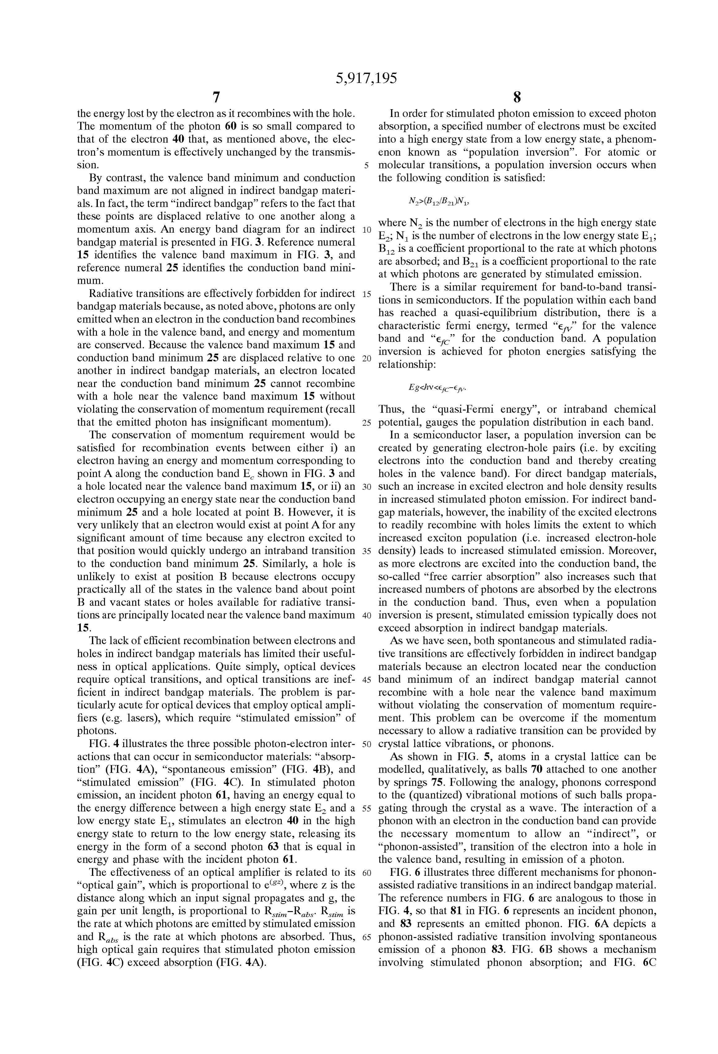
another in indirect bandgap materials, an electron located near the conduction band minimum 25 cannot recombine with a hole near the valence band maximum 15 without violating the conservation of momentum requirement (recall Thus, the “quasi-Fermi energy', or intraband chemical that the emitted photon has insignificant momentum). 25 potential, gauges the population distribution in each band. The conservation of momentum requirement would be In a Semiconductor laser, a population inversion can be satisfied for recombination events between either i) an created by generating electron-hole pairs (i.e. by exciting electron having an energy and momentum corresponding to electrons into the conduction band and thereby creating point A along the conduction band E shown in FIG. 3 and holes in the Valence band). For direct bandgap materials, a hole located near the valence band maximum 15, or ii) an Such an increase in excited electron and hole density results electron occupying an energy State near the conduction band in increased Stimulated photon emission. For indirect band minimum 25 and a hole located at point B. However, it is gap materials, however, the inability of the excited electrons very unlikely that an electron would exist at point A for any to readily recombine with holes limits the extent to which Significant amount of time because any electron excited to increased exciton population (i.e. increased electron-hole that position would quickly undergo an intraband transition 35 density) leads to increased stimulated emission. Moreover, to the conduction band minimum 25. Similarly, a hole is as more electrons are excited into the conduction band, the unlikely to exist at position B because electrons occupy So-called “free carrier absorption” also increases Such that practically all of the States in the Valence band about point increased numbers of photons are absorbed by the electrons B and vacant States or holes available for radiative transi in the conduction band. Thus, even when a population tions are principally located near the Valence band maximum 40 inversion is present, Stimulated emission typically does not 15. exceed absorption in indirect bandgap materials. The lack of efficient recombination between electrons and AS we have Seen, both Spontaneous and Stimulated radia holes in indirect bandgap materials has limited their useful tive transitions are effectively forbidden in indirect bandgap neSS in optical applications. Quite Simply, optical devices materials because an electron located near the conduction require optical transitions, and optical transitions are inef 45 band minimum of an indirect bandgap material cannot ficient in indirect bandgap materials. The problem is par recombine with a hole near the Valence band maximum ticularly acute for optical devices that employ optical ampli without violating the conservation of momentum require fiers (e.g. lasers), which require “stimulated emission” of ment. This problem can be overcome if the momentum photons. necessary to allow a radiative transition can be provided by FIG. 4 illustrates the three possible photon-electron inter 50 crystal lattice vibrations, or phonons. actions that can occur in Semiconductor materials: “absorp As shown in FIG. 5, atoms in a crystal lattice can be tion” (FIG. 4A), “spontaneous emission” (FIG. 4B), and modelled, qualitatively, as balls 70 attached to one another “stimulated emission” (FIG. 4C). In stimulated photon by Springs 75. Following the analogy, phonons correspond emission, an incident photon 61, having an energy equal to to the (quantized) vibrational motions of Such balls propa the energy difference between a high energy State E and a 55 gating through the crystal as a wave. The interaction of a low energy State E, stimulates an electron 40 in the high phonon with an electron in the conduction band can provide energy State to return to the low energy State, releasing its the necessary momentum to allow an “indirect', or energy in the form of a Second photon 63 that is equal in “phonon-assisted’, transition of the electron into a hole in energy and phase with the incident photon 61. the Valence band, resulting in emission of a photon. The effectiveness of an optical amplifier is related to its 60 FIG. 6 illustrates three different mechanisms for phonon “optical gain", which is proportional to e°, where Z is the assisted radiative transitions in an indirect bandgap material. distance along which an input signal propagates and g, the The reference numbers in FIG. 6 are analogous to those in gain per unit length, is proportional to R-R. R. is FIG. 4, so that 81 in FIG. 6 represents an incident phonon, the rate at which photons are emitted by Stimulated emission and 83 represents an emitted phonon. FIG. 6A depicts a and R is the rate at which photons are absorbed. Thus, 65 phonon-assisted radiative transition involving Spontaneous high optical gain requires that Stimulated photon emission emission of a phonon 83. FIG. 6B shows a mechanism (FIG. 4C) exceed absorption (FIG. 4A). involving stimulated phonon absorption; and FIG. 6C
Page 22
depicts a mechanism involving Stimulated phonon emission. emission can be enhanced. In Some instances, the resonator AS noted above, both momentum and energy must be may be able to Support a nonequilibrium phonon population conserved in a radiative transition. In each type of phonon that maintains itself through Stimulated phonon emission. assisted radiative transition depicted in FIG. 6, the phonon This is achieved when the phonon generation rate is equal to provides the requisite change in momentum, (ka-k), So the Scattering loSS for the Structure. momentum is conserved during recombination of an elec AS mentioned above, the energy of the photon emitted in tron in the conduction band minimum with a hole in the phonon-assisted radiative transitions has the value E=E+0 Valence band maximum. Consequently, a photon having an when the photon is produced by a mechanism involving energy approximately equal to the bandgap is emitted. phonon absorption, and has the value E=E-0 when the Specifically, the emitted photon has an energy, E. that is photon is produced by a mechanism involving phonon equal to the bandgap minus (for those mechanisms involving emission. Photons produced by a mechanism involving phonon emission) or plus (for mechanisms involving phonon absorption therefore have an energy greater than the phonon absorption) the phonon energy, 0. That is: bandgap energy. Such photons can readily be re-absorbed by E=Elite). the Structure. On the other hand, photons produced by a mechanism involving phonon emission have an energy leSS
Note that only phonons having the Specified momentum 15 than that of the bandgap and cannot readily be reabsorbed by (k-k) can assist in the radiative transition. the Structure. Thus, optical gain is more readily achieved in Unfortunately, radiative, phonon-assisted transitions are a phonon resonator in which photon emission occurs rare in conventional Semiconductor Structures. Furthermore, through a proceSS involving phonon emission rather than electrons in indirect bandgap materials tend to recombine phonon absorption. For recombination events involving with defects or impurities (traps) in the crystal before phonon emission, the enhancement of radiative transitions in recombining with a hole in the Valence band. Such electron a phonon resonator is equal to the number of phonons per trap recombination events are non-radiative and generate vibrational mode of the resonator.
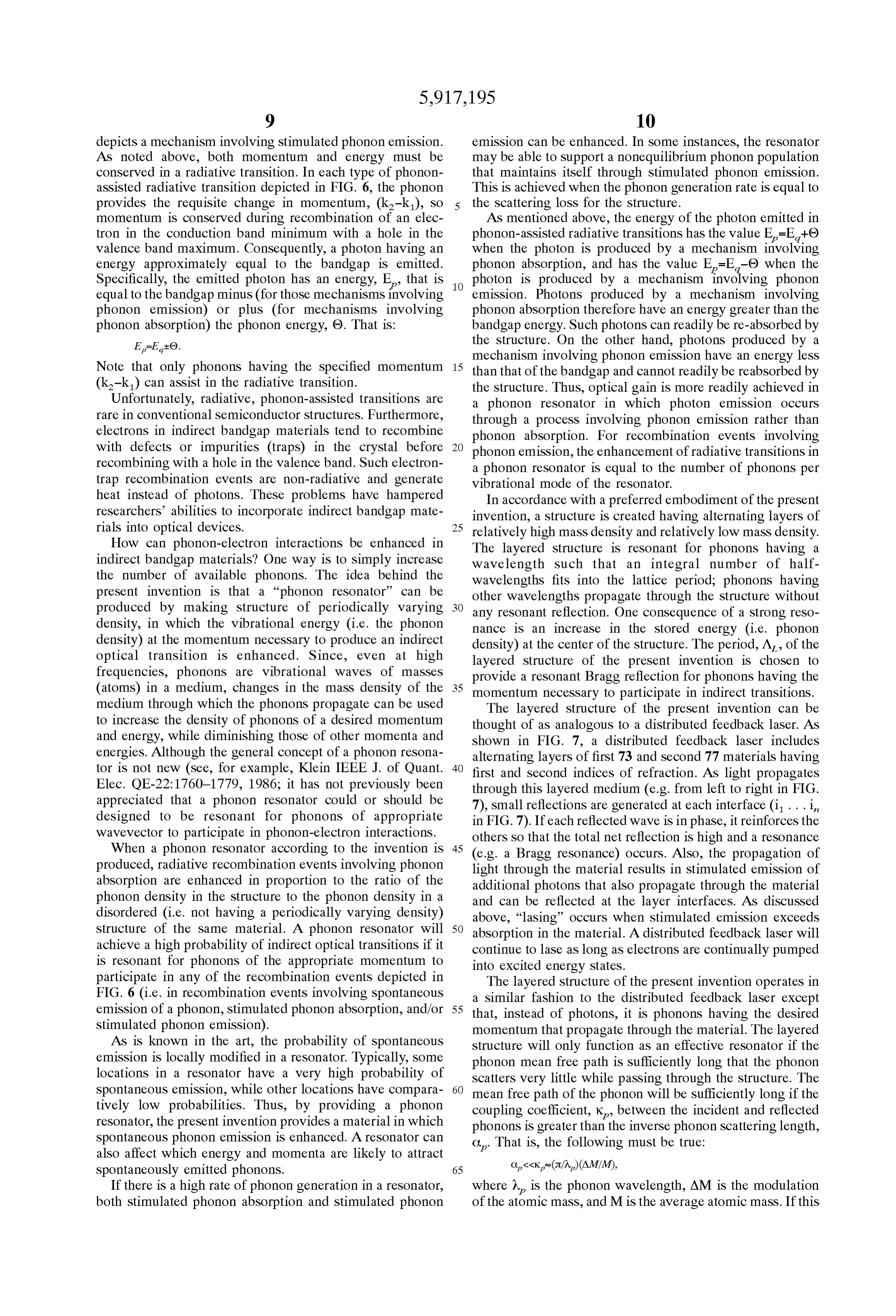
heat instead of photons. These problems have hampered In accordance with a preferred embodiment of the present researchers’ abilities to incorporate indirect bandgap mate invention, a structure is created having alternating layers of rials into optical devices. 25 relatively high mass density and relatively low mass density. How can phonon-electron interactions be enhanced in The layered Structure is resonant for phonons having a indirect bandgap materials? One way is to simply increase wavelength Such that an integral number of half the number of available phonons. The idea behind the wavelengths fits into the lattice period; phonons having present invention is that a "phonon resonator' can be other wavelengths propagate through the Structure without produced by making structure of periodically varying any resonant reflection. One consequence of a strong reso density, in which the vibrational energy (i.e. the phonon nance is an increase in the Stored energy (i.e. phonon density) at the momentum necessary to produce an indirect density) at the center of the structure. The period, A., of the optical transition is enhanced. Since, even at high layered structure of the present invention is chosen to frequencies, phonons are vibrational waves of masses provide a resonant Bragg reflection for phonons having the (atoms) in a medium, changes in the mass density of the 35 momentum necessary to participate in indirect transitions. medium through which the phonons propagate can be used The layered Structure of the present invention can be to increase the density of phonons of a desired momentum thought of as analogous to a distributed feedback laser. AS and energy, while diminishing those of other momenta and shown in FIG. 7, a distributed feedback laser includes energies. Although the general concept of a phonon resona alternating layers of first 73 and second 77 materials having tor is not new (see, for example, Klein IEEE J. of Quant. 40 first and Second indices of refraction. AS light propagates Elec. QE-22:1760–1779, 1986; it has not previously been through this layered medium (e.g. from left to right in FIG. appreciated that a phonon resonator could or should be designed to be resonant for phonons of appropriate 7), in
Small reflections are generated at each interface (i... i.
FIG. 7). If each reflected wave is in phase, it reinforces the wavevector to participate in phonon-electron interactions. otherS So that the total net reflection is high and a resonance When a phonon resonator according to the invention is 45 (e.g. a Bragg resonance) occurs. Also, the propagation of produced, radiative recombination events involving phonon light through the material results in Stimulated emission of absorption are enhanced in proportion to the ratio of the additional photons that also propagate through the material phonon density in the Structure to the phonon density in a and can be reflected at the layer interfaces. AS discussed disordered (i.e. not having a periodically varying density) above, "lasing occurs when Stimulated emission exceeds Structure of the Same material. A phonon resonator will 50 absorption in the material. A distributed feedback laser will achieve a high probability of indirect optical transitions if it continue to lase as long as electrons are continually pumped is resonant for phonons of the appropriate momentum to into excited energy States.
participate in any of the recombination events depicted in The layered Structure of the present invention operates in FIG. 6 (i.e. in recombination events involving spontaneous a similar fashion to the distributed feedback laser except emission of a phonon, Stimulated phonon absorption, and/or 55 that, instead of photons, it is phonons having the desired Stimulated phonon emission). momentum that propagate through the material. The layered AS is known in the art, the probability of Spontaneous Structure will only function as an effective resonator if the emission is locally modified in a resonator. Typically, Some phonon mean free path is Sufficiently long that the phonon locations in a resonator have a very high probability of Scatters very little while passing through the Structure. The Spontaneous emission, while other locations have compara 60 mean free path of the phonon will be sufficiently long if the tively low probabilities. Thus, by providing a phonon coupling coefficient, K, between the incident and reflected resonator, the present invention provides a material in which phonons is greater than the inverse phonon Scattering length, Spontaneous phonon emission is enhanced. A resonator can C. That is, the following must be true:
also affect which energy and momenta are likely to attract
Spontaneously emitted phonons. 65
If there is a high rate of phonon generation in a resonator, where 2 is the phonon wavelength, AM is the modulation both Stimulated phonon absorption and Stimulated phonon of the atomic mass, and M is the average atomic mass. If this
Page 23
relationship does not hold, phonons Scatter before Bragg increased in accordance with the present invention, the reflection can occur. exciton radiative lifetime is reduced. Accordingly, fewer The layered Structure of the present invention may be conduction electrons exist as free electrons, and more elec realized in a crystalline Solid, for example by alternating trons are available for exciton formation. thin, isotopically-enriched layers-i.e. by making an "iso When the exciton radiative lifetime is decreased, room tope Superlattice.” An "isotopically enriched” layer, as temperature excitonic interactions can occur in indirect defined herein, is a layer having a concentration of an bandgap materials, Such as Silicon. The free exciton binding isotope which is greater than the concentration of the isotope energy in materials. Such as Silicon is 14.7 meV, much larger found naturally. For example, in its naturally occurring form, than that observed in direct-gap materials Such as GaAS. Silicon is primarily composed of three isotopes in the Despite this fact, excitons do not exist in Silicon at room temperature. The primary reason for this is that, in Silicon, following compositions, 92.2% Si’, 4.7% Si” and 3.1% the rate of radiative transitions is much lower than the rate Si'. In accordance with the present invention, an of nonradiative band-to-band recombination processes. isotopically-enriched layer of Si is a layer that contains the isotope Si in a concentration more than 92.2% of the atoms Thus, phonon an increase in radiative transitions, as provided by a resonator of the present invention, will result in of that layer. Similarly, isotopically enriched layers of Sif' 15 Stable excitons at much higher temperatures. These stable and Si are layers that have atomic concentrations of these excitonic interactions can provide the basis for light isotopes that exceed 4.7% and 3.1%, respectively. emission, absorption, modulation, and nonlinear optical Isotope Superlattices are known in the art (See, for properties in Such indirect bandgap materials. For example, example, Berezin Solid State Comm. 65:819-821, 1988; the photon absorption of an exciton can change in the Berezin J. Phys. C. 20:L219–L221, 1987; Fuchs Sup. and presence of an electric field (Stark effect). Therefore, in Microstruct. 13: 447–458, 1993; Haller GADEST, '93). accordance with the present invention, an optical modulator However, it has not previously been recognized that isotope based on the Stark effect can be made of indirect bandgap Superlattices can be engineered to be phonon resonators that materials.
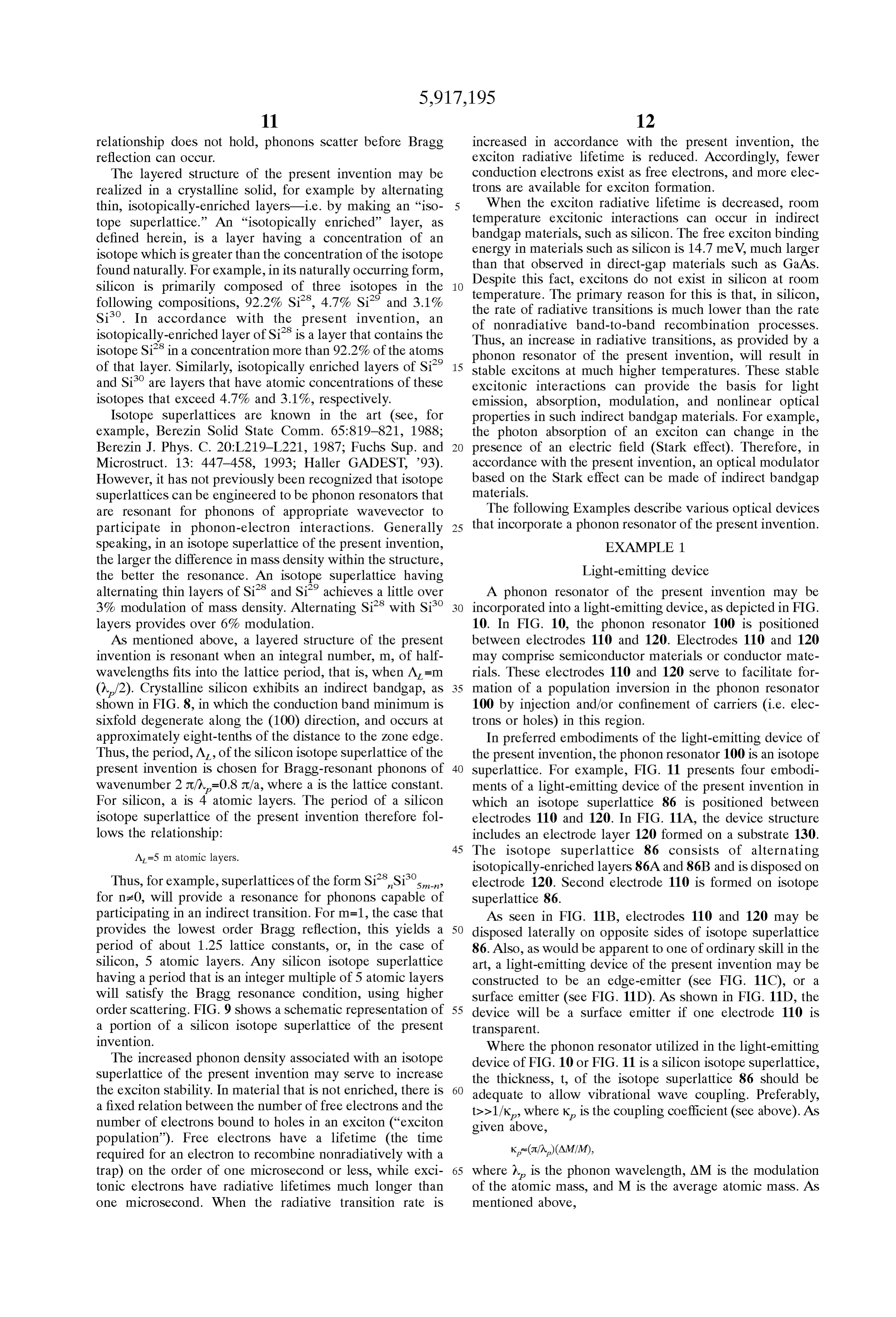
are resonant for phonons of appropriate wavevector to The following Examples describe various optical devices participate in phonon-electron interactions. Generally 25 that incorporate a phonon resonator of the present invention. Speaking, in an isotope Superlattice of the present invention, EXAMPLE 1. the larger the difference in mass density within the Structure, Light-emitting device the better the resonance. An isotope Superlattice having alternating thin layers of Si and Siachieves a little over A phonon resonator of the present invention may be 3% modulation of mass density. Alternating Si with Si incorporated into a light-emitting device, as depicted in FIG. layers provides over 6% modulation. 10. In FIG. 10, the phonon resonator 100 is positioned AS mentioned above, a layered Structure of the present between electrodes 110 and 120. Electrodes 110 and 120 invention is resonant when an integral number, m, of half may comprise Semiconductor materials or conductor mate wavelengths fits into the lattice period, that is, when A =m rials. These electrodes 110 and 120 serve to facilitate for (1/2). Crystalline silicon exhibits an indirect bandgap, as 35 mation of a population inversion in the phonon resonator shown in FIG. 8, in which the conduction band minimum is 100 by injection and/or confinement of carriers (i.e. elec Sixfold degenerate along the (100) direction, and occurs at trons or holes) in this region. approximately eight-tenths of the distance to the Zone edge. In preferred embodiments of the light-emitting device of Thus, the period, A., of the Silicon isotope Superlattice of the the present invention, the phonon resonator 100 is an isotope present invention is chosen for Bragg-resonant phonons of 40 Superlattice. For example, FIG. 11 presents four embodi wavenumber 2 /2=0.8 JL/a, where a is the lattice constant. ments of a light-emitting device of the present invention in For Silicon, a is 4 atomic layers. The period of a Silicon which an isotope Superlattice 86 is positioned between isotope Superlattice of the present invention therefore fol electrodes 110 and 120. In FIG. 11A, the device structure lows the relationship: includes an electrode layer 120 formed on a substrate 130. 45 The isotope Superlattice 86 consists of alternating
A=5 m atomic layers.
isotopically-enriched layers 86A and 86B and is disposed on
Thus, for example, Superlattices of the form Si Si's electrode 120. Second electrode 110 is formed on isotope for nz0, will provide a resonance for phonons capable of Superlattice 86.
participating in an indirect transition. For m=1, the case that As seen in FIG. 11B, electrodes 110 and 120 may be provides the lowest order Bragg reflection, this yields a 50 disposed laterally on opposite sides of isotope Superlattice period of about 1.25 lattice constants, or, in the case of 86. Also, as would be apparent to one of ordinary skill in the Silicon, 5 atomic layers. Any Silicon isotope Superlattice art, a light-emitting device of the present invention may be having a period that is an integer multiple of 5 atomic layers constructed to be an edge-emitter (see FIG. 11C), or a will Satisfy the Bragg resonance condition, using higher surface emitter (see FIG. 11D). As shown in FIG. 11D, the order Scattering. FIG. 9 shows a Schematic representation of 55 device will be a Surface emitter if one electrode 110 is a portion of a Silicon isotope Superlattice of the present transparent.
invention. Where the phonon resonator utilized in the light-emitting The increased phonon density associated with an isotope device of FIG. 10 or FIG. 11 is a silicon isotope Superlattice, Superlattice of the present invention may serve to increase the thickness, t, of the isotope Superlattice 86 should be the exciton Stability. In material that is not enriched, there is 60 adequate to allow vibrational wave coupling. Preferably, a fixed relation between the number of free electrons and the number of electrons bound to holes in an exciton (“exciton t>>1/K, where K is the coupling coefficient (see above). AS given above, population”). Free electrons have a lifetime (the time required for an electron to recombine nonradiatively with a Ke(I/W)(AM/M), trap) on the order of one microsecond or less, while exci 65 where 2 is the phonon wavelength, AM is the modulation tonic electrons have radiative lifetimes much longer than of the atomic mass, and M is the average atomic mass. AS one microSecond. When the radiative transition rate is mentioned above,
Page 24
A =m(W/2). The main technical requirement for overall efficiency in an LED such as that depicted in FIG. 12 is a high radiative
Thus, quantum efficiency (the average number of photons emitted
per electron-hole pair injected). In preferred embodiments of the LED of the present invention, high radiative quantum
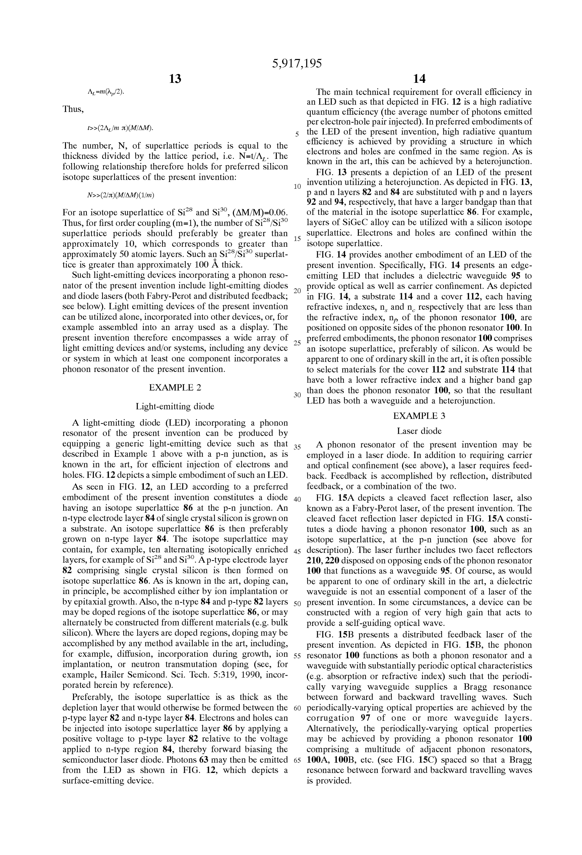
The number, N, of Superlattice periods is equal to the efficiency is achieved by providing a structure in which thickness divided by the lattice period, i.e. N=t/A. The electrons and holes are confmed in the same region. AS is following relationship therefore holds for preferred silicon known in the art, this can be achieved by a heterojunction. FIG. 13 presents a depiction of an LED of the present isotope Superlattices of the present invention: invention utilizing a heterojunction. AS depicted in FIG. 13, p and n layers 82 and 84 are substituted with p and n layers 92 and 94, respectively, that have a larger bandgap than that
For an isotope superlattice of Si° and Si, (AM/M)=0.06. of the material in the isotope Superlattice 86. For example, Thus, for first order coupling (m=1), the number of Si/Si' layers of SiGeC alloy can be utilized with a silicon isotope Superlattice periods should preferably be greater than 15 Superlattice. Electrons and holes are confined within the approximately 10, which corresponds to greater than isotope Superlattice.
approximately 50 atomic layers. Such an Si/Sisuperlat FIG. 14 provides another embodiment of an LED of the tice is greater than approximately 100 A thick. present invention. Specifically, FIG. 14 presents an edge Such light-emitting devices incorporating a phonon reso emitting LED that includes a dielectric waveguide 95 to nator of the present invention include light-emitting diodes provide optical as well as carrier confinement. AS depicted and diode lasers (both Fabry-Perot and distributed feedback; in FIG. 14, a substrate 114 and a cover 112, each having See below). Light emitting devices of the present invention refractive indexes, n and n respectively that are less than can be utilized alone, incorporated into other devices, or, for the refractive index, ne, of the phonon resonator 100, are example assembled into an array used as a display. The positioned on opposite sides of the phonon resonator 100. In present invention therefore encompasses a wide array of 25 preferred embodiments, the phonon resonator 100 comprises light emitting devices and/or Systems, including any device an isotope Superlattice, preferably of Silicon. AS would be or System in which at least one component incorporates a apparent to one of ordinary skill in the art, it is often possible phonon resonator of the present invention. to select materials for the cover 112 and Substrate 114 that
EXAMPLE 2
have both a lower refractive indeX and a higher band gap than does the phonon resonator 100, so that the resultant
Light-emitting diode LED has both a waveguide and a heterojunction.
EXAMPLE 3
A light-emitting diode (LED) incorporating a phonon resonator of the present invention can be produced by Laser diode equipping a generic light-emitting device Such as that 35 A phonon resonator of the present invention may be described in Example 1 above with a p-n junction, as is employed in a laser diode. In addition to requiring carrier known in the art, for efficient injection of electrons and and optical confinement (See above), a laser requires feed holes. FIG. 12 depicts a simple embodiment of such an LED. back. Feedback is accomplished by reflection, distributed As seen in FIG. 12, an LED according to a preferred feedback, or a combination of the two.
embodiment of the present invention constitutes a diode 40 FIG. 15A depicts a cleaved facet reflection laser, also having an isotope Superlattice 86 at the p-n junction. An known as a Fabry-Perot laser, of the present invention. The n-type electrode layer 84 of Single crystal Silicon is grown on cleaved facet reflection laser depicted in FIG. 15A consti a Substrate. An isotope Superlattice 86 is then preferably tutes a diode having a phonon resonator 100, Such as an grown on n-type layer 84. The isotope Superlattice may isotope Superlattice, at the p-n junction (See above for contain, for example, ten alternating isotopically enriched 45 description). The laser further includes two facet reflectors layers, for example of Si and Si. A p-type electrode layer 210, 220 disposed on opposing ends of the phonon resonator 82 comprising Single crystal Silicon is then formed on 100 that functions as a waveguide 95. Of course, as would isotope Superlattice 86. AS is known in the art, doping can, be apparent to one of ordinary skill in the art, a dielectric in principle, be accomplished either by ion implantation or waveguide is not an essential component of a laser of the by epitaxial growth. Also, the n-type 84 and p-type 82 layers 50 present invention. In Some circumstances, a device can be may be doped regions of the isotope Superlattice 86, or may constructed with a region of very high gain that acts to alternately be constructed from different materials (e.g. bulk provide a Self-guiding optical wave. Silicon). Where the layers are doped regions, doping may be FIG. 15B presents a distributed feedback laser of the accomplished by any method available in the art, including, present invention. As depicted in FIG. 15B, the phonon for example, diffusion, incorporation during growth, ion 55 resonator 100 functions as both a phonon resonator and a implantation, or neutron transmutation doping (see, for waveguide with Substantially periodic optical characteristics example, Hailer Semicond. Sci. Tech. 5:319, 1990, incor (e.g. absorption or refractive index) Such that the periodi porated herein by reference). cally varying waveguide Supplies a Bragg resonance Preferably, the isotope Superlattice is as thick as the between forward and backward travelling waves. Such depletion layer that would otherwise be formed between the 60 periodically-varying optical properties are achieved by the p-type layer 82 and n-type layer 84. Electrons and holes can corrugation 97 of one or more waveguide layers. be injected into isotope Superlattice layer 86 by applying a Alternatively, the periodically-varying optical properties positive Voltage to p-type layer 82 relative to the Voltage may be achieved by providing a phonon resonator 100 applied to n-type region 84, thereby forward biasing the comprising a multitude of adjacent phonon resonators, semiconductor laser diode. Photons 63 may then be emitted 65 100A, 100B, etc. (see FIG. 15C) spaced so that a Bragg from the LED as shown in FIG. 12, which depicts a resonance between forward and backward travelling waves Surface-emitting device. is provided.
Page 25
EXAMPLE 4 phase, or frequency of the light. The detector, in turn, is designed to convert the information into electrical impulses
Vertical cavity Surface emitting laser Suitable for further Signal processing. In other embodiments A phonon resonator of the present invention may also be of the present optical communication System, a phonon incorporated into a vertical cavity Surface emitting laser resonator of the present invention is incorporated into a (VECSEL). As depicted in FIG. 16, a VECSEL of the laser, an optical amplifier, a modulator, a Switch, a deflector, present invention comprises a top reflector 122 and a bottom and/or a Scanner.
reflector 124 positioned around a phonon resonator 100 as a AS is well known in the art, optical communications can p-n junction (see above). Electrodes 110 and 120 are posi be useful for long distance communications, local area tioned acroSS the p-n junction and Serve to inject current into networks, optical data Storage, and/or broadcast Services the phonon resonator 100, thereby creating optical gain. Such as cable television. Such Systems are also useful for The bottom reflector reflects approximately 100% of interconnections among and within circuit boards and inte incident radiation and comprises alternating layers of mate grated circuits.
rials having different refractive indices, n and n. Each layer 15 EXAMPLE 7 has a thickness equal to 2/2, where 2 is the wavelength of the amplified radiation. The thickness, t, of the bottom reflec Self-Sustained oscillator for phonons and photons tor 124 follows the relationship:
A phonon resonator of the present invention can be constructed So that it Satisfies known requirements for
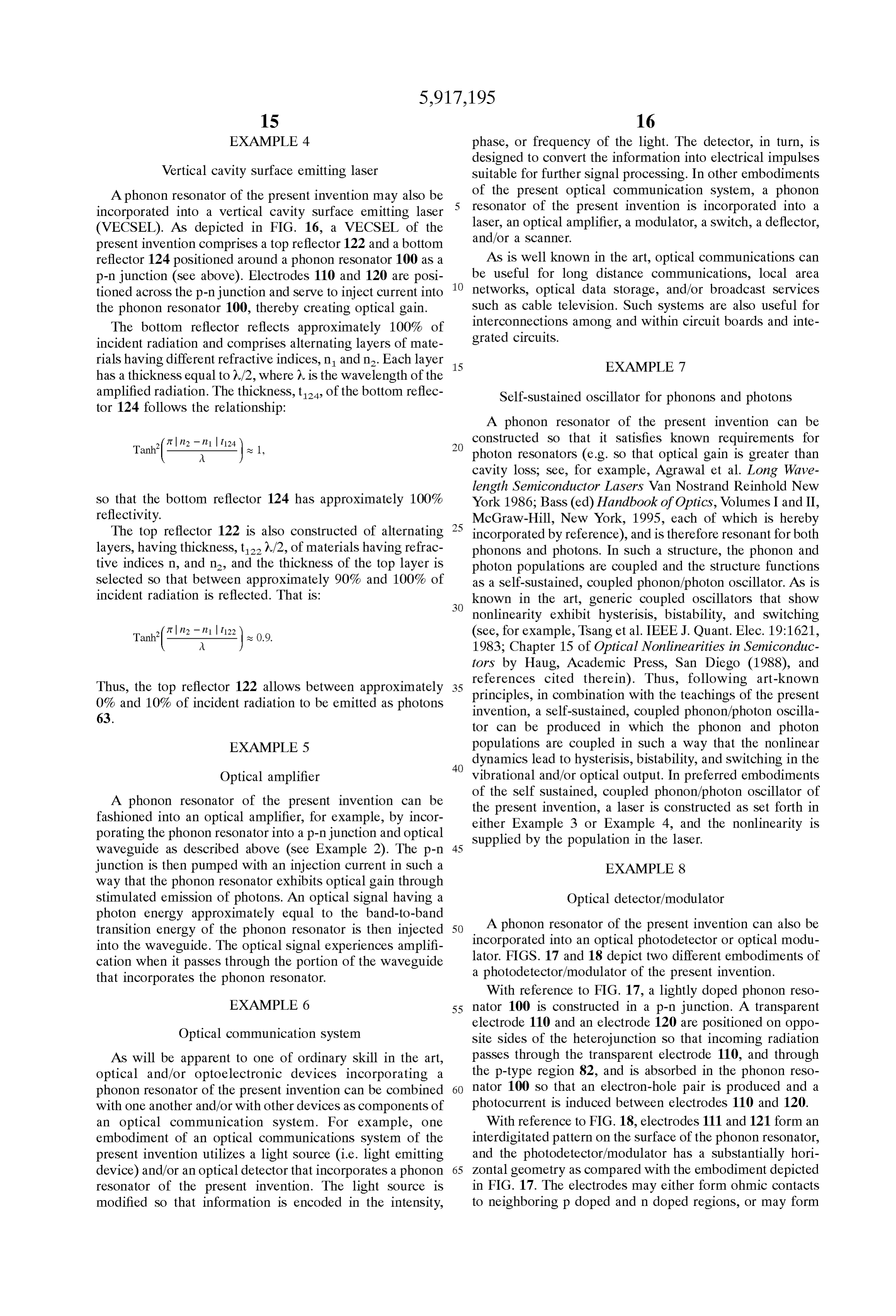
Tan (le le) & 1, photon resonators (e.g. So that optical gain is greater than cavity loSS; See, for example, Agrawal et al. Long Wave length Semiconductor Lasers Van Nostrand Reinhold New so that the bottom reflector 124 has approximately 100% York 1986; Bass (ed) Handbook of Optics, Volumes I and II, reflectivity. McGraw-Hill, New York, 1995, each of which is hereby The top reflector 122 is also constructed of alternating 25 incorporated by reference), and is therefore resonant for both layers, having thickness, t2, 2/2, of materials having refrac phonons and photons. In Such a Structure, the phonon and tive indices n, and n, and the thickness of the top layer is photon populations are coupled and the Structure functions selected so that between approximately 90% and 100% of as a Self-Sustained, coupled phonon/photon oscillator. AS is incident radiation is reflected. That is: known in the art, generic coupled oscillators that show nonlinearity exhibit hysterisis, bistability, and Switching (see, for example, Tsang et al. IEEE J. Quant. Elec. 19:1621,
Tan (i.e. - in le as 0.9. 1983; Chapter 15 of Optical Nonlinearities in Semiconduc tors by Haug, Academic Press, San Diego (1988), and
Thus, the top reflector 122 allows between approximately 35 references cited therein). Thus, following art-known principles, in combination with the teachings of the present 0% and 10% of incident radiation to be emitted as photons invention, a Self-Sustained, coupled phonon/photon oscilla
tor can be produced in which the phonon and photon
EXAMPLE 5 populations are coupled in Such a way that the nonlinear
dynamics lead to hysterisis, bistability, and Switching in the
Optical amplifier Vibrational and/or optical output. In preferred embodiments A phonon resonator of the present invention can be of the the Self Sustained, coupled phonon/photon oscillator of present invention, a laser is constructed as Set forth in fashioned into an optical amplifier, for example, by incor either porating the phonon resonator into a p-n junction and optical SuppliedExample by the 3 or Example 4, and the nonlinearity is population in the laser.
waveguide as described above (see Example 2). The p-n 45 junction is then pumped with an injection current in Such a EXAMPLE 8 way that the phonon resonator exhibits optical gain through
Stimulated emission of photons. An optical Signal having a Optical detector/modulator photon energy approximately equal to the band-to-band
A phonon resonator of the present invention can also be transition energy of the phonon resonator is then injected 50 incorporated into the waveguide. The optical Signal experiences amplifi into an optical photodetector or optical modu cation when it passes through the portion of the waveguide lator. FIGS. 17 and 18 depict two different embodiments of that incorporates the phonon resonator. a photodetector/modulator of the present invention. With reference to FIG. 17, a lightly doped phonon reso
EXAMPLE 6 55 nator 100 is constructed in a p-n junction. A transparent electrode 110 and an electrode 120 are positioned on oppo
Optical communication System Site sides of the heterojunction So that incoming radiation AS will be apparent to one of ordinary skill in the art, passes through the transparent electrode 110, and through optical and/or optoelectronic devices incorporating a the p-type region 82, and is absorbed in the phonon reso phonon resonator of the present invention can be combined 60 nator 100 so that an electron-hole pair is produced and a with one another and/or with other devices as components of photocurrent is induced between electrodes 110 and 120. an optical communication System. For example, one With reference to FIG. 18, electrodes 111 and 121 form an embodiment of an optical communications System of the interdigitated pattern on the Surface of the phonon resonator, present invention utilizes a light Source (i.e. light emitting and the photodetector/modulator has a Substantially hori device) and/or an optical detector that incorporates a phonon 65 Zontal geometry as compared with the embodiment depicted resonator of the present invention. The light Source is in FIG. 17. The electrodes may either form ohmic contacts modified So that information is encoded in the intensity, to neighboring p doped and n doped regions, or may form
Page 26
Schottky contacts to a uniformly doped phonon resonators. available, electronic exchanges can occur between electrons One advantage of this design is that it permits high Speed in different, degenerate, conduction band minima. In pre Switching or detection due to the close proximity of the ferred embodiments of the present invention, electron Scat electrodes, and therefore to the short transit time required to tering is provided by interaction between an electron and a communicate between them. phonon of appropriate wavenumber. FIG. 22 depicts an Enhancement of Electrical Properties example of Such an exchange event, termed "intervalley The present invention also relates to indirect bandgap Scattering, occurring between opposite, degenerate conduc materials having enhanced electrical properties. Specifically, tion band minima.
the invention encompasses materials having enhanced In the case presented in FIG. 22, an electron is Scattered conductivity, including Superconductivity, due to the pres from a state A (wavenumber k) to a state B (wavenumber ence of bound electron pairs. In order that certain aspects -k), upon interaction with a phonon of wavenumber 2 TL/A, and advantages of the present invention will be more readily where A, is the period of the Semiconductor material lattice. appreciated, we begin with a discussion of the properties of Thus, the matrix element can be expressed as: conduction band electrons, and electron-phonon interactions, in Semiconductor materials. 15
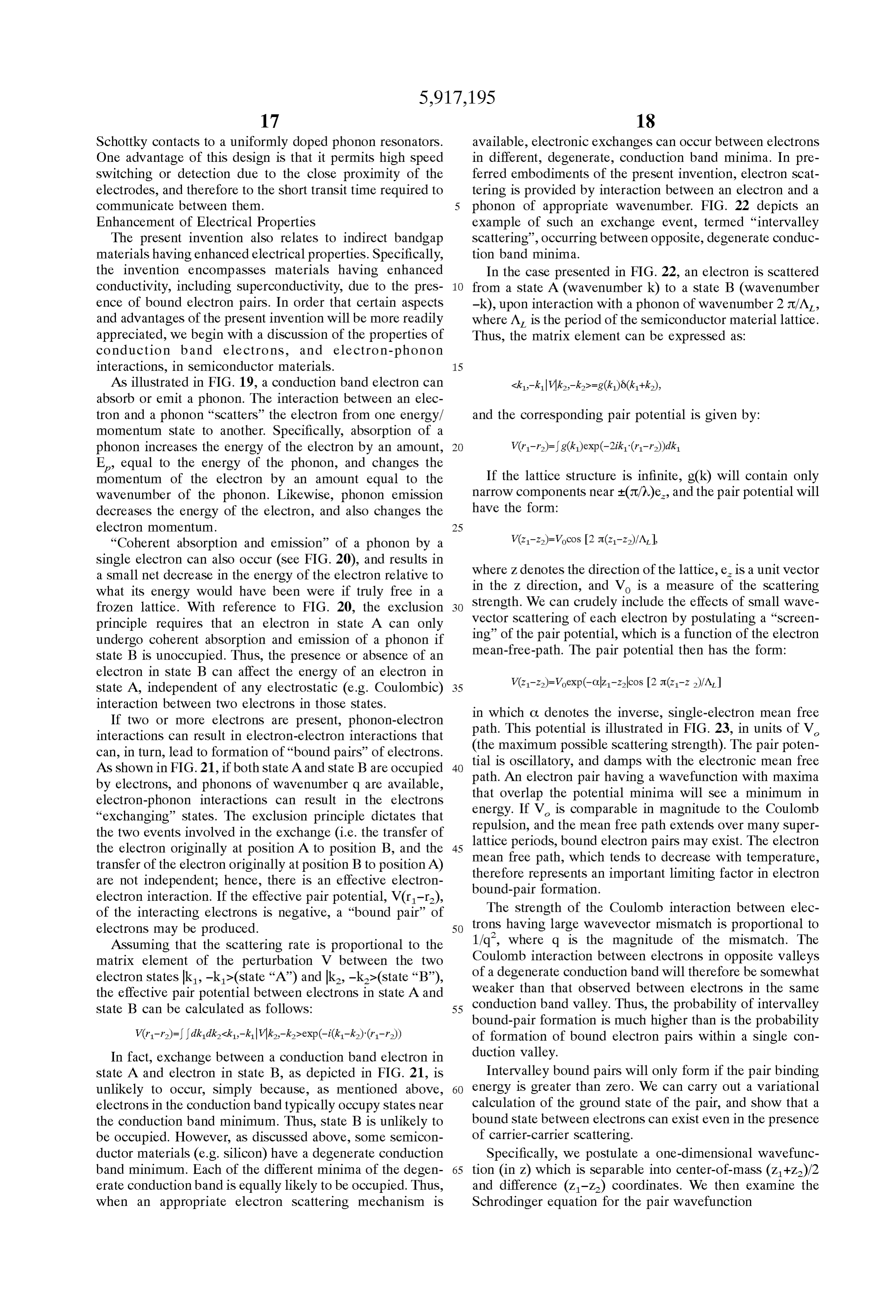
As illustrated in FIG. 19, a conduction band electron can <k-kVIk-k->=g(k)ö(k+k), absorb or emit a phonon. The interaction between an elec tron and a phonon “Scatters' the electron from one energy/ and the corresponding pair potential is given by: momentum State to another. Specifically, absorption of a phonon increases the energy of the electron by an amount, V(r-r)= g(k)exp(-2ik (r-r))dk E, equal to the energy of the phonon, and changes the momentum of the electron by an amount equal to the If the lattice structure is infinite, g(k) will contain only wavenumber of the phonon. Likewise, phonon emission narrow components near t(t/l)e, and the pair potential will decreases the energy of the electron, and also changes the have the form:
electron momentum. 25 “Coherent absorption and emission” of a phonon by a V(21-22)=Vocos 2 J(21-22)/All Single electron can also occur (see FIG. 20), and results in where Z denotes the direction of the lattice, e is a unit vector a Small net decrease in the energy of the electron relative to what its energy would have been were if truly free in a in the Z direction, and Vo is a measure of the Scattering frozen lattice. With reference to FIG. 20, the exclusion strength. We can crudely include the effects of Small wave principle requires that an electron in State A can only vector Scattering of each electron by postulating a “Screen undergo coherent absorption and emission of a phonon if ing” of the pair potential, which is a function of the electron State B is unoccupied. Thus, the presence or absence of an mean-free-path. The pair potential then has the form: electron in State B can affect the energy of an electron in
State A, independent of any electrostatic (e.g. Coulombic) 35 interaction between two electrons in those States.
If two or more electrons are present, phonon-electron in which C. denotes the inverse, Single-electron mean free interactions can result in electron-electron interactions that path. This potential is illustrated in FIG. 23, in units of V. (the maximum can, in turn, lead to formation of “bound pairs of electrons. tial is oscillatory, possible Scattering strength). The pair poten As shown in FIG. 21, if both state A and state B are occupied 40 and damps with the electronic mean free by electrons, and phonons of wavenumber q are available, path. An electron pair having a wavefunction with maxima that overlap the potential minima will See a minimum in electron-phonon interactions can result in the electrons energy.
“exchanging States. The exclusion principle dictates that repulsion,If and V is comparable in magnitude to the Coulomb the two events involved in the exchange (i.e. the transfer of lattice periods, the mean free path extends over many Super the electron originally at position A to position B, and the 45 mean free path,bound which electron pairs may exist. The electron tends to decrease with temperature, transfer of the electron originally at position B to position A) therefore represents an important limiting factor in electron are not independent; hence, there is an effective electron bound-pair formation.
electron interaction. If the effective pair potential, V(r-ra), of the interacting electrons is negative, a “bound pair of The strength of the Coulomb interaction between elec electrons may be produced. 50 trons having large wavevector mismatch is proportional to ASSuming that the Scattering rate is proportional to the 1/q, where q is the magnitude of the mismatch. The matrix element of the perturbation V between the two Coulomb interaction between electrons in opposite Valleys electron Statesk, -ki>(state “A”) and k2, -k->(state “B”), weaker of a degenerate conduction band will therefore be Somewhat the effective pair potential between electrons in State A and than that observed between electrons in the same state B can be calculated as follows: 55 conduction band valley. Thus, the probability of intervalley bound-pair formation is much higher than is the probability of formation of bound electron pairs within a single con
In fact, exchange between a conduction band electron in duction Valley.
State A and electron in State B, as depicted in FIG. 21, is Intervalley bound pairs will only form if the pair binding unlikely to occur, Simply because, as mentioned above, 60 energy is greater than Zero. We can carry out a variational electrons in the conduction band typically occupy States near calculation of the ground State of the pair, and Show that a the conduction band minimum. Thus, state B is unlikely to bound State between electrons can exist even in the presence be occupied. However, as discussed above, Some Semicon of carrier-carrier Scattering.
ductor materials (e.g. Silicon) have a degenerate conduction Specifically, we postulate a one-dimensional wavefunc band minimum. Each of the different minima of the degen 65 tion (in Z) which is separable into center-of-mass (Z+z)/2 erate conduction band is equally likely to be occupied. Thus, and difference (Z-Z.) coordinates. We then examine the when an appropriate electron Scattering mechanism is Schrodinger equation for the pair wavefunction
Page 27
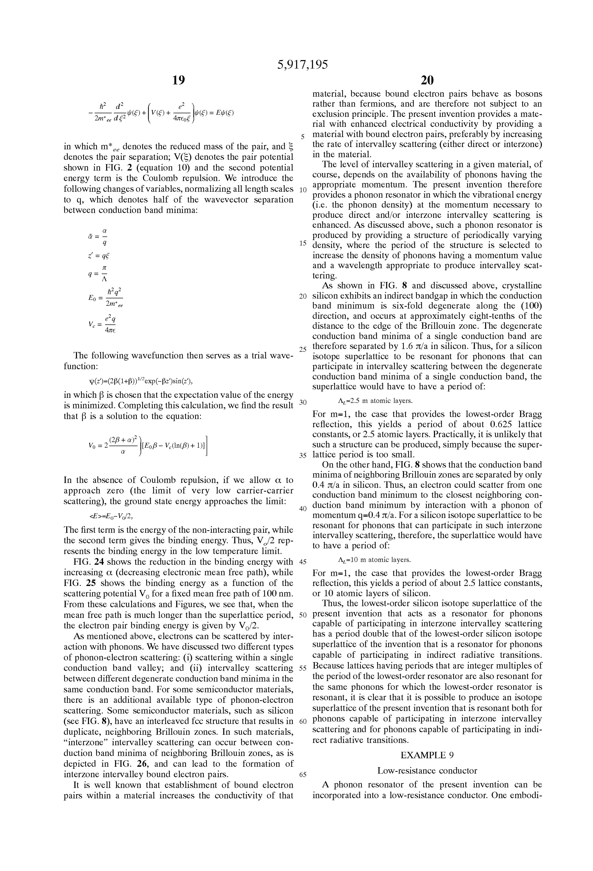
material, because bound electron pairs behave as bosons i2 p2 rather than fermions, and are therefore not Subject to an 2n re's) -(ve -- e = Eff() exclusion principle. The present invention provides a mate rial with enhanced electrical conductivity by providing a material with bound electron pairs, preferably by increasing in which me denotes the reduced mass of the pair, and S the rate of intervalley Scattering (either direct or interZone) denotes the pair separation; V(S) denotes the pair potential in the material.
shown in FIG. 2 (equation 10) and the second potential The level of intervalley Scattering in a given material, of energy term is the Coulomb repulsion. We introduce the course, depends on the availability of phonons having the following changes of variables, normalizing all length Scales appropriate momentum. The present invention therefore to q, which denotes half of the wavevector Separation provides a phonon resonator in which the vibrational energy between conduction band minima: (i.e. the phonon density) at the momentum necessary to produce direct and/or interZone intervalley Scattering is
enhanced. AS discussed above, Such a phonon resonator is d = - produced by providing a Structure of periodically varying i 15 density, where the period of the Structure is Selected to g = q. increase the density of phonons having a momentum value and a wavelength appropriate to produce intervalley Scat q= x tering.
i2 2 As shown in FIG. 8 and discussed above, crystalline E = 2nce 2 Silicon exhibits an indirect bandgap in which the conduction band minimum is six-fold degenerate along the (100)
2 direction, and occurs at approximately eight-tenths of the V. = 47te2 distance to the edge of the Brillouin Zone. The degenerate conduction band minima of a Single conduction band are 25 therefore Separated by 1.6 L/a in Silicon. Thus, for a Silicon
The following wavefunction then serves as a trial wave isotope Superlattice to be resonant for phonons that can function: participate in intervalley Scattering between the degenerate conduction band minima of a single conduction band, the
Superlattice would have to have a period of:
in which B is chosen that the expectation value of the energy A=2.5 m atomic layers.
is minimized. Completing this calculation, we find the result that B is a Solution to the equation: For m=1, the case that provides the lowest-order Bragg reflection, this yields a period of about 0.625 lattice (2/3+ a) constants, or 2.5 atomic layers. Practically, it is unlikely that Such a structure can be produced, simply because the Super 35 lattice period is too Small.
On the other hand, FIG. 8 shows that the conduction band
In the absence of Coulomb repulsion, if we allow C. to minima of neighboring Brillouin Zones are Separated by only 0.4 JL/a in Silicon. Thus, an electron could Scatter from one approach Zero (the limit of very low carrier-carrier conduction
Scattering), the ground State energy approaches the limit: 40 duction bandband minimum to the closest neighboring con minimum by interaction with a phonon of momentum q=0.4 JL/a. For a Silicon isotope Superlattice to be
The first term is the energy of the non-interacting pair, while resonant for phonons that can participate in Such interZone the Second term gives the binding energy. Thus, V/2 rep intervalley Scattering, therefore, the Superlattice would have resents the binding energy in the low temperature limit. to have a period of:
FIG. 24 shows the reduction in the binding energy with 45 A=10 m atomic layers.
increasing C. (decreasing electronic mean free path), while For m=1, the case that provides the lowest-order Bragg FIG. 25 shows the binding energy as a function of the reflection, this yields a period of about 2.5 lattice constants, Scattering potential Vo for a fixed mean free path of 100 nm. or 10 atomic layers of Silicon.
From these calculations and Figures, we see that, when the Thus, the lowest-order Silicon isotope Superlattice of the mean free path is much longer than the Superlattice period, 50 present invention that acts as a resonator for phonons the electron pair binding energy is given by Vo/2. capable of participating in interZone intervalley Scattering AS mentioned above, electrons can be Scattered by inter has a period double that of the lowest-order Silicon isotope action with phonons. We have discussed two different types Superlattice of the invention that is a resonator for phonons of phonon-electron Scattering: (i) scattering within a single capable of participating in indirect radiative transitions. conduction band Valley; and (ii) intervalley Scattering 55 Because lattices having periods that are integer multiples of between different degenerate conduction band minima in the the period of the lowest-order resonator are also resonant for Same conduction band. For Some Semiconductor materials, the same phonons for which the lowest-order resonator is there is an additional available type of phonon-electron resonant, it is clear that it is possible to produce an isotope Scattering. Some Semiconductor materials, Such as Silicon Superlattice of the present invention that is resonant both for (see FIG. 8), have an interleaved fec structure that results in 60 phonons capable of participating in interZone intervalley duplicate, neighboring Brillouin Zones. In Such materials, Scattering and for phonons capable of participating in indi “interZone' intervalley Scattering can occur between con rect radiative transitions.
duction band minima of neighboring Brillouin Zones, as is EXAMPLE 9 depicted in FIG. 26, and can lead to the formation of Low-resistance conductor interZone interValley bound electron pairs. 65
It is well known that establishment of bound electron A phonon resonator of the present invention can be pairs within a material increases the conductivity of that incorporated into a low-resistance conductor. One embodi
Page 28
ment of Such a low-resistance conductor, is depicted in FIG. useful combination of components may be utilized, and 27. As depicted in FIG. 27, two devices 230a, b are related components that do not incorporate a phonon reso connected by means of a phonon resonator 100, that carries nator may be used in combination with components that do electrical signals between the devices 230a, b. As would be utilize a phonon resonator for enhanced electrical conduc readily apparent to one of ordinary skill in the art, it may be tion.
desirable to dope the low-resistance conductor of the present Accelerated Heat Transfer from a Phonon Resonator invention, or other devices discussed herein. In Such cases, Electron-phonon interactions can be thought of as a doping may be accomplished by any method available in the Source by which nonequilibrium phonons are generated. art, including, for example, diffusion, incorporation during Thus, electron-phonon interactions can provide the gain growth, ion implantation, or neutron transmutation doping mechanism necessary to achieve the vibrational analog of (see, for example, Haller Semicond. Sci. Tech. 5:319, 1990, laser action in a resonator. Once Such a phonon resonator incorporated herein by reference). reaches threshold, the emitted energy becomes both coher ent and highly directional. A phonon resonator operating
EXAMPLE 10 above threshold can therefore provide accelerated heat trans fer from the resonator to the Substrate on which the resonator
Planar transformer resides via the coherent, directional emission of vibrational energy to the Substrate.
AS is known in the art, a planar transformer is formed Further, just as a variety of Systems exhibit Stochastic when at least two conducting pathways are arranged with resonances in the presence of nonlinearities, vibrational respect to one another, e.g. in a Serpentine configuration, So anharmonicities combined with a phonon resonator would that alternating current flow is provided. A phonon resonator be expected to exhibit Stochastic resonances. These reso nances are both coherent and directional, providing accel of the present invention can be incorporated into one or more erated heat transfer from (or through) an isotope Superlattice. of the conducting pathways, to produce a planar transformer with enhanced electrical conductivity, and therefore Method A of Producing a Phonon Resonator phonon resonator of the present invention can be enhanced magnetic properties. Of course, a phonon resona 25 tor of the present invention could also be incorporated into fabricated by any of a variety of methods. We describe here other devices whose magnetic properties Stem from electri the preparation of an isotope Superlattice phonon resonator. There are two aspects to any method of producing an isotope cal conductivity. Superlattice: i) providing separate, Substantially pure iso EXAMPLE 11 topes, and ii) assembling the Substantially pure isotopes in a layered Structure of the invention. These two aspects can be
Diode performed Separately or simultaneously.
Available methods for isotope Separation include, among
A phonon resonator of the present invention can be others, gaseous diffusion, gas centrifuge, fractional incorporated into a diode as depicted in FIG. 28. The phonon distillation, aerodynamic Separation, chemical eXchange, resonator 100 is incorporated into a p-n junction to form a 35 electromagnetic Separation, and laser dissociation/ionization diode with enhanced electrical properties. Contacts 240a, (see, for, example London Separation of Isotopes, London: and b are shown positioned on opposite sides of the junction. George Newnes, Ltd., 1961; Spindel et al. J. Chem. Engin.
EXAMPLE 12
J. AM Chem. Soc. 108: 5760, 1986; Stevenson et al. Nature
Bipolar Transistor 323:522, 1986; Bigelelsen Science 147: 463, 1965; Tanaka
et al. Nature 341: 727, 1989; Ambartzumion Applied Optics,
FIG. 29 depicts a npn bipolar transistor incorporating a11, p. 354, 1972; N. R. Isenor et al. Can. J. Phys. 51:1281, phonon resonator of the present invention. The base 250 of 1973; Epling et al. Am. Chem. Soc. 103:1238, 1981; the transistor comprises a phonon resonator 100 that Kamioka et al. J. Phys. Chem.90:5727, 1986; Lyman et al. enhances conduction between the emitter 260 and the col 45 J. App. Phys. 47:595, 1976; Arai et al. Appl. Phys. B53:199, lector 270. 1991; Clark et al. Appl. Phys. Lett. 32:46, 1978, each of which is incorporated herein by reference). Also, float Zone
EXAMPLE 13 Segregation may be utilized for purification of a Semicon ductor.
Field Effect Transistor 50 Methods available for assembling isotopically pure mate rials into an isotope Superlattice of the present invention
FIG. 30 depicts a n-type Junction Field Effect Transistor include, for example, chemical vapor deposition (CVD), (JFET) incorporating a phonon resonator of the present invention. The gate 310 comprises a phonon resonator 100 molecular
(CBE) beam epitaxy (MBE), and chemical beam epitaxy (see, for example, Sedwicket al J. Vac Sci. Technol.
that enhances conduction between Source 320 and drain 330. 55
AS would be apparent to one of ordinary skill in the art, a A 10(4), 1992, incorporated herein by reference). Isotopi phonon resonator could also be incorporated into an cally pure materials prepared by any available method, n-channel Metal Oxide Semiconductor Field Effect Transis including those recited above, may be used in combination with standard CVD, MBE, or CBE technologies to produce tor (MOSFET) (see FIG. 31). an isotope Superlattice of the present invention.
EXAMPLE 1.4
60 Additionally, an isotope Superlattice of the present inven tion may be prepared by performing isotope Separation and
Integrated circuit layer deposition simultaneously. In a particularly preferred embodiment of the present invention, the laser dissociation
FIG. 32 depicts an integrated circuit utilizing a combina isotope Separation technique is utilized in combination with tion of the above-described components (e.g. a low 65 a CVD process, (i.e. as a “laser-assisted CVD” process) in resistance conductor, a diode, a bipolar transistor, a JFET, a single chamber, to produce an isotope Superlattice of the and/or a MOSFET) incorporating a phonon resonator. Any present invention (see Example 18).
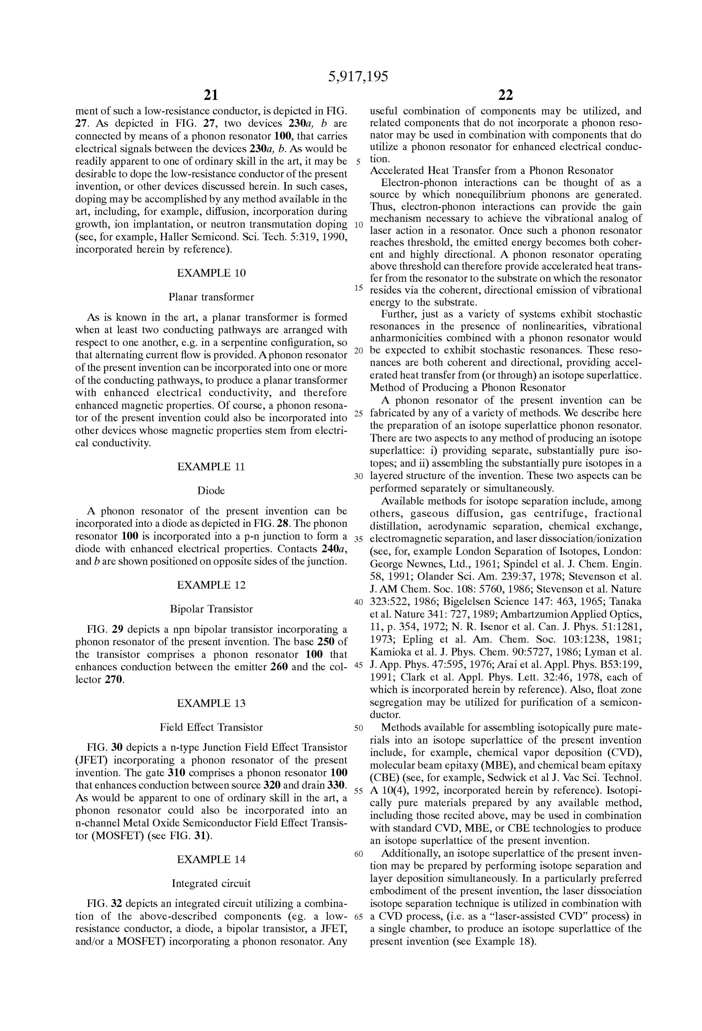
Page 29
Examples 15-18 provide Specific descriptions of frac In order to Separate one isotope of an atom from another tional distillation, chemical eXchange, laser dissociation, and using laser dissociation, a mixture of molecules including laser-assisted CVD techniques, respectively. Fractional dis the different isotopes is bombarded with radiation (i.e. from tillation can be utilized, for example, in the preparation of a laser) tuned to the vibrational transition frequency of a first bulk precursors for epitaxial or Czochralski growth. Laser molecule including a first isotope. The first molecule there assisted CVD provides in Situ isotope Separation and layer fore becomes excited and can be separated from other growth. These examples are descriptions of preferred molecules in the mixture by Virtue of its higher temperature, embodiments, and are not intended to limit the Scope of the or its increased sensitivity to photodissociation (see below). invention as a whole. After the first isotope has been isolated, the radiation fre 1O quency can be adjusted by, for example, tuning the laser to
EXAMPLE 1.5 a new frequency or providing an alternate laser Source, So Fractional Distillation that the radiation frequency is tuned to the vibrational transition frequency of a Second molecule, including a
It is well known that there exist slight differences in the Second isotope, and that Second molecule can be isolated. heat of vaporization of different isotopic Species contained 15 The procedure is repeated until all desired isotopes are in a liquid. The method of fractional distillation provides, isolated.
after processing, for one isotopic Species to remain in the liquid phase while the other is drawn off in a vapor phase. EXAMPLE 1.8 A preferred method for the Separation of Silicon isotopes Laser-assisted CVD would be the fractional distillation of SiCl, a material which is liquid at room temperature but which provides a com A Silicon isotope Superlattice of the present invention may paratively high vapor pressure. Since SiCl is a Standard be produced by exposing Silane (SiH) gas to infrared precursor for production of both Silane and elemental radiation in a chamber such as that depicted in FIG. 21. A Silicon, there is very little waste in this proceSS. wafer 300 is held in the chamber at a temperature below that
EXAMPLE 16
required for Spontaneous decomposition of Silane. The wafer 300 may be positioned on a heater 350. A first laser 310 is
Chemical Exchange tuned to the vibrational transition frequency of the first desired silicon isotope (e.g. Sif). The laser excitation pro
Chemical eXchange provides Separation between different vides a large temperature differential between the desired isotopic Species by virtue of isotopic differences in free isotope and the other isotopes, resulting in deposition of only energy and the corresponding influence on equilibrium the desired isotope on the wafer 300. Alternatively, the first chemical reactions. It has been shown that, under Suitable laser 310 can be used to excite only the first desired silicon circumstances, isotopic species will show different ratios in isotope, and a Second laser 320 can provide a high energy reactant and product mixtures for certain equilibrium reac photon to photoionize the excited Silane molecules (i.e. tions. The key requirements for Such chemical eXchange 35 those Silane molecules containing the desired Silicon mechanisms to be effective are: isotope), producing ions that have high reactivity with the The use of immiscible reactant/product phases Surface of the wafer 300.
(immiscible liquids or liquid-gas reactions); After the appropriate number of atomic layers of the first Electronic orbitals similar to the delocalized orbitals 40 silicon isotope have been laid down, the first laser 310 is found in aromatic compounds, and adjusted and tuned to the vibrational transition frequency of An appropriate catalyst to Speed the reaction to equilib the second desired silicon isotope (e.g. Si"). The appropri rium. ate number of atomic layers of the Second Silicon isotope are then laid down. The process is reiterated until the desired 45 isotope Superlattice Structure is produced.
EXAMPLE 1.7
Laser dissociation and isotope-Selective heating After the growth of the isotope Superlattice, calibration of layer thickness can be carried out through a SIMS analysis.
Laser dissociation and isotope-Selective heating is the Standard in situ monitoring (e.g. RHEED) can also be preferred method for in Situ Separation and growth of carried out to determine, for example, if the majority isotope isotope-pure layers. 50 layerS grow at a dramatically faster rate than the minority The laser dissociation technique of isotope Separation isotope layers. If So, the disparity can be corrected, for relies on the fact that many molecules exhibit vibrational example, by adjusting the laser power (e.g. lowering the transitions in the near- to mid- infrared range. Bombarding laser power for depositing the majority isotope layers). molecules with radiation tuned to their vibrational transi At all times during the growth of the isotope Superlattice tions dissociates the molecules. Because the vibrational 55 of the present invention, the temperature in the chamber transitions of molecules are dependent on the masses of the should be high enough to maintain the Surface mobility of atoms, molecules containing different isotopes of a given deposited Silicon atoms, in order to assure epitaxial growth. atom exhibit different transition energies. Thus, molecules It is also preferred that the isotope Superlattice be grown in containing different isotopes of a given atom are dissociated the direction of the lowest conduction band minimum. For by bombardment with radiation of different frequencies. 60 silicon, this corresponds to the (100)(010)(001) family of A variety of laser Sources are available with access to the growth planes; for germanium, a (111) Superlattice is desir near- to mid- infrared region, that could be used to dissociate able. Diamond has a band Structure closer to that of Silicon, molecules having vibrational transitions in that region. For and therefore requires Similar growth directions. AS would example, transitions in the 9-10 um range are accessible be apparent to one of ordinary skill in the art, other growth using a CO laser, various Solid State lasers can access the 65 directions are possible, provided that the periodicity in the near-infrared; and optical parametric oscillator technology appropriate direction (e.g. in the (100) direction for Silicon) can be utilized to achieve wide tunability. meets the criteria discussed herein.
Page 30
The isotope purity of an isotope Superlattice of the present AS will be apparent to one of ordinary skill in the art, a invention can be tested using any available method Such as, Structure of periodically varying density Such as that for example, Secondary ion mass spectroScopy or Raman described herein could be designed to Suppress, rather than Scattering. to enhance, phonons of particular wavevectors. For AS will be appreciated by one of ordinary skill in the art, example, it is Sometimes desirable to avoid phonon-electron important requirements for production of an isotopically interactions that result in ionization of an electron bound in pure Superlattice of the present invention include the a quantum well or a quantum wire Structure. A Structure of requirement that the wafer 300 be atomically clean, that the the present invention can be assembled as described herein, Switching of laser frequencies does not lead to deposition of having been designed not to be resonant for, and therefore to “mixed' isotopic layers, and that the chamber provide a 1O SuppreSS, phonons at the energies required to ionize an Substantially collision-free environment. electron. Such a structure would improved the performance Each of these requirements is discussed in turn. First of of the quantum well or wire.
all, the wafer 300 can be cleaned using standard methods AS will also be apparent to one of ordinary skill in the art, and oxide removal should be performed. an isotope Superlattice of the present invention could be In order to avoid problems associated with mixed isotope 15 constructed from isotopically enriched layers of two or more populations produced during laser tuning, one particular different elements or compounds, provided that the overall embodiment of the method of the present invention provides Structure is designed to be resonant for phonons of appro a plurality of wafers 300 assembled onto a rotating carousel priate wavevector to participate in phonon-electron interac whose rotation is timed Such that only pure isotope layers are tions. For example, a structure could be assembled compris deposited on wafers (i.e. So that mixed populations are ing two atomic layers of a carbon isotope alternating with produced during the times that gaps, instead of wafers, are three atomic layers of a Silicon isotope. Such a structure exposed to the Silane Stream). would exhibit a large (greater than approximately 2.5 eV) A Substantially collision-free environment is ensured in indirect bandgap, and would be Suitable for use in, for example, a light emitting device Such as those described the method of the present invention, as depicted in FIG. 21, herein.
by having the first 310 and second 320 lasers intersect at a 25 point close to the surface of the wafer 300. The above-described preferred embodiment of the AS will also be appreciated by one of ordinary skill in the method of the invention utilizes Silane (SiH) as a starting art, it is desirable when practicing the preferred method of material to produce a Silicon isotope Superlattice of the the present inventors to ensure that Silicon layers are depos invention by laser-assisted isotope Separation. Other starting ited preferentially if not uniquely, on the wafer 300, and not materials could also be used Such as, for example, SiHCl, on other parts of the chamber. Thus, it is desirable that the SiF, or any other member of the halide-silane family of infrared windows 330 and 340, through which the first and gases, although heavier molecules Such as dichlorosilane Second laser beams are directed, be made of a material that (SiH,Cl) have complicated vibrational spectra, which will not be coated with silicon following the excitation. makes identification of a vibrational absorption frequency 35 that is clearly associated with a single Silicon isotope is more
OTHER EMBODIMENTS difficult. Thus, for the purposes of the present invention, The foregoing has provided a description of certain pre Silane is the preferred Source gas for laser-assisted isotope ferred embodiments of the present invention, which descrip Separation.
tion is not meant to be limiting. Other embodiments of the Also, while the Examples presented herein describe the present invention are within the Scope of the following 40 fabrication and application of one dimensional phonon claims. resonators, one of ordinary skill in the art would recognize In particular, the present invention is not limited to that structures that are periodic in more than one (e.g. in two Semiconductor materials. Materials. Such as diamond may or three dimensions can also be fabricated and used in also be used. Additionally, a phonon resonator may be accordance with the present teachings. Such structures pro incorporated into any of a variety of other optical or elec 45 vide resonances for phonons in up to three directions in the trical devices, as would readily be appreciated by one of crystal. The method for determining the resonator period in ordinary skill in the art. For example, a phonon resonator two or three dimensions is precisely analogous to that used may be incorporated into a Superconducting quantum inter for one dimension. A three dimensional periodicity has the ference device (SQUID), a Josephson junction, a high effect of modifying the phonon Spectrum of the entire crystal frequency transistor, or a microwave detector, in order to 50 rather than the phonon Spectrum in one dimension. enhance the electrical and/or thermal properties of those I claim:
devices. 1. A Silicon Structure of Substantially periodically varying Also, the present specification describes a Structure of density comprising:
periodically varying density (e.g. an isotope Superlattice). at least one first layer that is Substantially enriched for a The density of the preferred structure described above is 55 first Silicon isotope and has a first density; and varied by providing alternating layers of material of different at least one Second layer that is Substantially enriched for mass density. Another way to periodically vary the mass a Second Silicon isotope and has a Second density, Said density of a structure is to introduce a Standing wave into the first and Second layers being adjacent one another and Structure. However, because phonons normally only propa alternating in Said structure So that Said Structure has a gate 100-1000 A without Scattering, a Sound wave having a 60 Substantially periodically varying density in one wavelength of much less than 1000 A would be required to dimension, the period of Said structure being Selected establish the necessary Standing wave. Such Sound waves Such that Said Structure is Substantially resonant for cannot practically be generated. Thus, the preferred embodi phonons of appropriate wavevector to participate in ment of the Structure of periodically varying density of the electron-phonon interactions that change the interact present invention is a structure having layers of material of 65 ing electron's momentum.
different density, most preferably an isotope Superlattice as 2. The Structure of claim 1, further comprising at least one described herein. dopant.
Page 31
3. The structure of claim 1 wherein said first isotope is 18. The structure of claim 17 wherein said phonons Si and said second isotope is Si’. generated by Stimulated emission are coherent. 4. The structure of claim 1 wherein said first isotope is 19. The structure of claim 16 wherein said structure Si' and said second isotope is Si'. provides accelerated heat transfer. 5. The structure of claim 1 wherein said first isotope is 20. The structure of claim 16 wherein said element has Si” and said second isotope is Si. adjacent Brillouin Zones.
6. The structure of claim 3 having a period that is an 21. The structure of claim 16 wherein said first element integer multiple of five atomic layers. and Said Second element are the Same and Said first isotope 7. The structure of claim 1 wherein said structure provides and Said Second isotope represent different isotopes of that a stochastic phonon resonance.
8. A structure of Substantially periodically varying density element.
22. The structure of claim 21 wherein said element comprising:
comprises Silicon.
at least one first layer having a first density by Virtue of being enriched for a first isotope of a first element; and Si 23.andThe structure of claim 22 wherein said first isotope is said second isotope is Si.
at least one Second layer having a Second density by Virtue 24. The structure of claim 23 having a period that is an of being enriched for a Second isotope of a Second integer multiple of five atomic layers.
element, Said first and Second regions being adjacent 25. The structure of claim 22 wherein said first isotope is one another and alternating in Said structure So that Said Si' and said second isotope is Si’.
Structure has a Substantially periodically varying den 26. The structure of claim 22 wherein said first isotope is sity in one dimension the period of Said Structure being Si” and said second isotope is Si.
Selected Such that Said structure is Substantially reso 27. The structure of any one of claims 8 or 16 wherein nant for phonons of appropriate wavevector to partici Said first element and Said Second element are different. pate in radiative electronic transitions. 28. The structure of claim 27 wherein: 9. The structure of claim 8 wherein said first element and 25 Said first element comprises carbon;
Said Second element are the same and Said first isotope and Said Second element comprises Silicon; Said Second isotope represent different isotopes of that element. Said at least one first layer comprises two atomic layers 10. The structure of claim 9 wherein said element is an enriched for a first carbon isotope, and indirect bandgap material. Said at least one Second layer comprises three atomic 11. The structure of claim 9 wherein said element com layers enriched for a first Silicon isotope. prises Silicon. 29. A silicon structure having: 12. The structure of claim 11 wherein said first isotope is degenerate conduction band Valleys, and Si' and said second isotope is Si. Substantially periodic variations in material composition, 13. The structure of claim 12 having a period that is an 35 Said Substantially periodic variations comprising alter integer multiple of five atomic layers. nations of a first layer substantially enriched for a first 14. The structure of claim 11 wherein said first isotope is Silicon isotope and a Second layer Substantially Si and said second isotope is Si’. enriched for a Second Silicon isotope So that Said 15. The structure of claim 11 wherein said first isotope is material composition varies in one dimension, the Si' and said second isotope is Si’. 40 periodicity of the layers being Selected So that Scatter 16. A structure of Substantially periodically varying den ing of electrons between Said degenerate conduction sity comprising: band Valleys is enhanced relative to intervalley electron at least one first region having a first density by Virtue of Scattering in a structure lacking Said Substantially peri being enriched for a first isotope of a first element; and odic variations.
at least one Second region having a Second density by 45 30. The structure of claim 29 wherein said first isotope is Virtue of being enriched for a Second isotope of a Si and said second isotope is Si.
Second element, Said first and Second regions being 31. The structure of claim 30, further including doping adjacent one another and alternating in Said structure So atoms produced by neutron transmutation of said Si. that Said structure has a Substantially periodically vary 32. The structure of claim 29 wherein said first isotope is ing density, the period of Said Structure being Selected 50 Si' and said second isotope is Si’.
Such that Said Structure is Substantially resonant for 33. The structure of claim 29 wherein said first isotope is phonons generated by Stimulated emission. Si” and said second isotope is Si. 17. The structure of claim 16 wherein said phonons generated by Stimulated emission are directional. k k k k k
Provenance
- Collection
- Cited prior art
- Original PDF
- patentimages.storage.googleapis.com →
- Filed
- 1995-02-17
- Pages
- 31
- Method
- pdftotext (the PDF's own text layer) + pdftoppm 300dpi page scans
- Source
- Google Patents bibliographic record
- Granted
- 1999-06-29
- Inventors
- Thomas G. Brown; Painter B A III
- Transcribed from
- patentimages.storage.googleapis.com →