patent · US5757833
Semiconductor laser having a transparent light emitting section, and a process of producing the same
26 May 1998
Page 1 — bibliographic record
United States Patent (19) 11 Patent Number: 5,757,833 Arakawa et al. 45 Date of Patent: May 26, 1998 54). SEMICONDUCTOR LASER HAVING A 5,574.289 11/1996 Aoki et al. ................................ 372/50 TRANSPARENT LIGHT EMITTING 5,657,338 8/1997 Kitamura ...................... ..., 372/50 SECTION, AND A PROCESS OF PRODUCING FOREIGN PATENT DOCUMENTS
THE SAME
2-62090 3/1990 Japan ....................................... 372/46 75 Inventors: Satoshi Arakawa; Norihiro Iwai, both 4-303982. A 10/1992 Japan.
of Tokyo: Takuya Ishikawa. Kawasaki; 6-196797 A 7/1994 Japan.
Akihiko Kasukawa, Tokyo; Michio OTHER PUBLICATIONS
Ohkubo, Fujisawa; Takao Ninomiya.
Yokohama, all of Japan Article entitled "High power. A1GaAs buried heterostruc ture lasers with flared waveguides”. by D.F. Welch et al.
73) Assignee: The Furukawa Electric Co., Ltd., Appl. Phys. Lett... vol. No. 50. No. 5, 2 Feb. 1987. Tokyo, Japan Primary Examiner-Rodney B. Bovernick
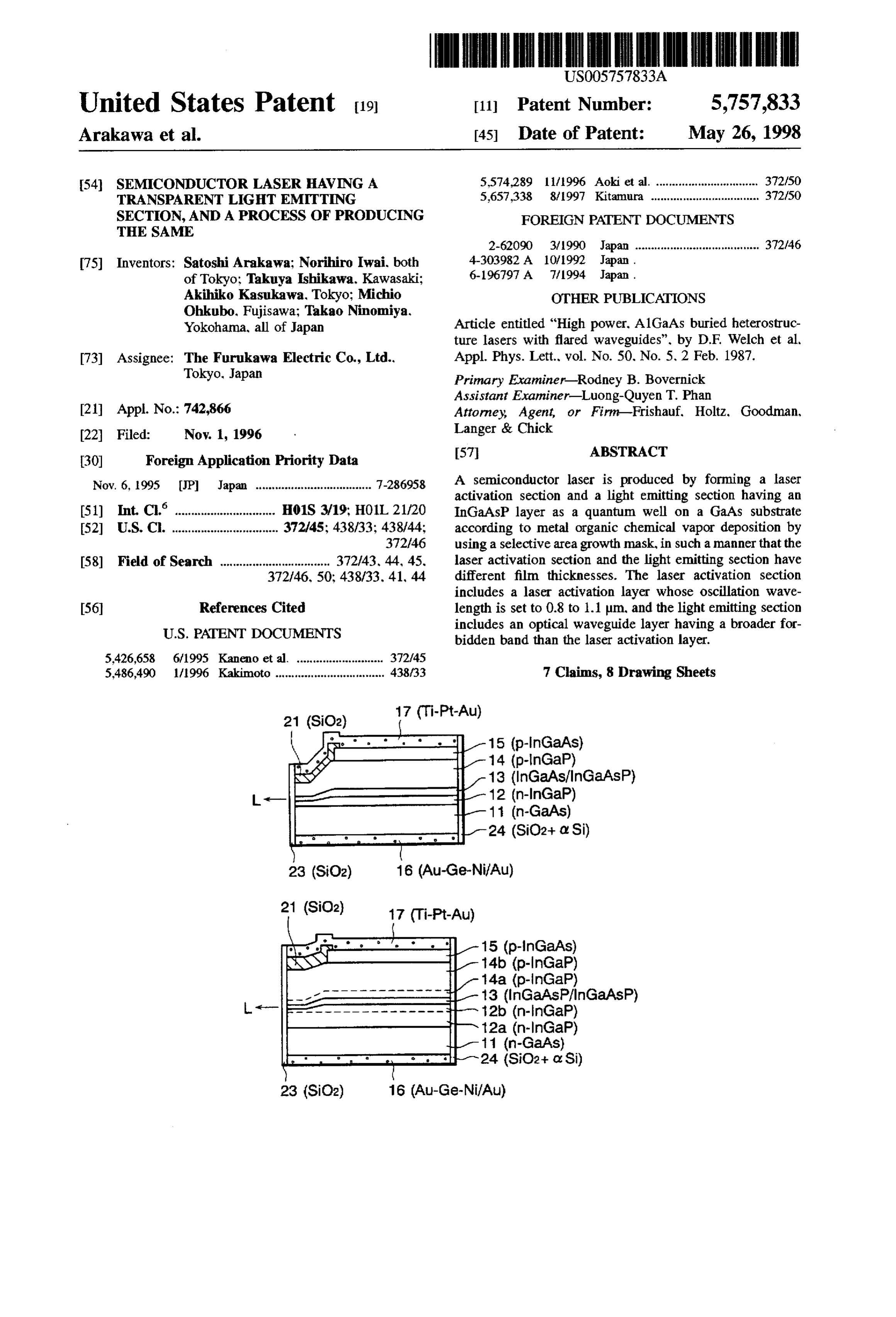
Assistant Examiner-Luong-Quyen T. Phan (21) Appl. No.: 742,866 Attorney, Agent, or Firm-Frishauf. Holtz. Goodman. 22 Filed: Nov. 1, 1996 Langer & Chick 30 Foreign Application Priority Data 57 ABSTRACT Nov. 6, 1995 (JP Japan ................................... 7-286958 A semiconductor laser is produced by forming a laser activation section and a light emitting section having an (51) Int. Cl. ................... H01S 3/19; HO1L 21/20 InGaAsP layer as a quantum well on a GaAs substrate 52 U.S.C. ................................. 372/45; 438/33; 438/44; according to metal organic chemical vapor deposition by 372/46 using a selective area growth mask, in such a manner that the 58) Field of Search .................................. 372/43, 44, 45. laser activation section and the light emitting section have 372/46, 50: 438/33. 41, 44 different film thicknesses. The laser activation section includes a laser activation layer whose oscillation wave 56 References Cited length is set to 0.8 to 1.1 um, and the light emitting section
includes an optical waveguide layer having a broader for bidden band than the laser activation layer.
5,426,658 6/1995 Kaneno et al. ........................... 372/45 5,486,490 1/1996 Kakimoto ................................. 438/33 7 Claims, 8 Drawing Sheets
Page 2
Drawing sheet — no readable text.
Page 3
Drawing sheet — no readable text.
Page 4
Drawing sheet — no readable text.
Page 5
Drawing sheet — no readable text.
Page 6
Drawing sheet — no readable text.
Page 7
Drawing sheet — no readable text.
Page 8
Drawing sheet — no readable text.
Page 9
Drawing sheet — no readable text.
Page 10
SEMCONDUCTOR LASER HAVING A devices of monolithic structure, wherein a dielectric mask TRANSPARENT LIGHT EMTTNG with a varying width is selectively formed on an InP SECTION, AND A PROCESS OF PRODUCING substrate in such a manner that a semiconductor laser region THE SAME and a modulator region to be formed on the substrate are situated between the mask regions, and a multilayer film is
BACKGROUND OF THE INVENTION grown by metal organic chemical vapor deposition on the 1. Field of the Invention
InP substrate having the mask formed thereon, so that the multilayer film has different thicknesses at the semiconduc
The present invention relates to a semiconductor laser tor laser region and the modulator region and its activation provided with a light emitting section which has transpar O layer has different bandgap energy levels at these regions. ency with respect to the laser oscillation wavelength and The metal organic chemical vapor deposition process using which also can emit a narrow circular beam with a large spot a selective area growth mask as disclosed in these publica size, and more particularly, to a semiconductor laser of tions makes the thickness of the multilayer film and the monolithic structure suited for obtaining higher light output. bandgap energy locally vary in accordance with the mask The present invention also relates to a simplified process for 15 width, and thus is very useful in producing semiconductor producing such a semiconductor laser, devices.
2. Description of the Related Art In the case of fabricating a high-output semiconductor In general, if the light output of a semiconductor laser laser with an oscillation wavelength of 0.8 to 1.1 p.m. a with a structure having for example. InGap layers and device structure is usually employed in which an InCaAs InGaAs layers formed on a GaAs substrate is increased, 20 layer is grown as a quantum well on a GaAs substrate. Since catastrophic optical damage is caused or the characteristics the InGaAs layer has a small indium (In) content, however, of the semiconductor laser deteriorate. It is therefore difficult a sufficient masking effect cannot be achieved even if a to increase the light output, and conventional semiconductor multilayer film is grown on the GaAs substrate by the metal laser devices generally have a maximum light output of organic chemical vapor deposition process using a selective about 200 mW. 25 area growth mask. Namely, the thickness of the InGaAs To solve the problem, it has been proposed to provide a layer on the GaAs substrate cannot be greatly changed, semiconductor laser with a light emitting section which has making it impossible to impart sufficient transparency to the transparency with respect to the laser oscillation wave light emitting section. Also, if the proportion of indium (In) length. For example, an attempt has been made to form a 30 in the InGaAs layer is increased, another problem arises in thin film of a material having large bandgap energy by that large strain is caused.
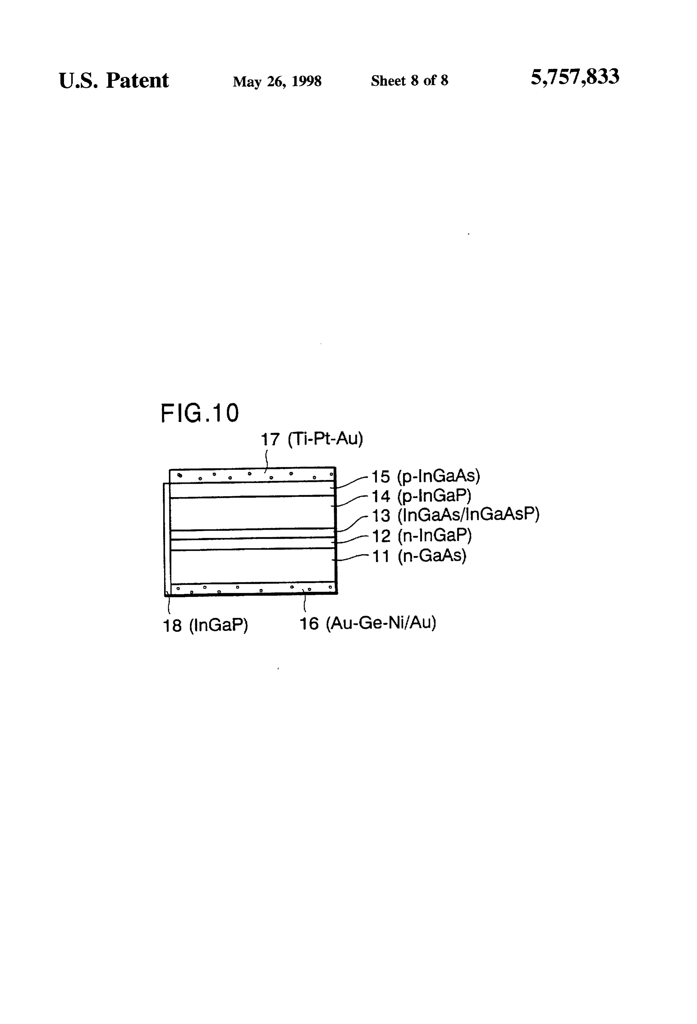
epitaxial growth on a light emitting surface, which is an end SUMMARY OF THE INVENTION face obtained by vertically cleaving a multilayer film formed on the substrate, so as to impart transparency active at the An object of the present invention is to provide a semi laser oscillation wavelength to the light emitting section and 35 conductor laser with a monolithic structure which has a thereby prevent the catastrophic optical damage (COD). transparent light emitting section and which permits increase FIG. 10 illustrates a typical example of conventional of the light output, and also to provide a simplified process semiconductor laser structure. This semiconductor laser has for producing such semiconductor lasers with improved a multilayer structure obtained by successively forming. on yield.
a GaAs substrate 11. an n-type InGap layer 12 serving as a 40 A semiconductor laser according to the present invention lower cladding layer, an InCaAs/InGaAsP layer 13 includ has a device structure wherein a multilayer film including an ing a strain quantum well and serving as a laser activation InGaAsP layer as a quantum well is grown on a GaAs layer, a p-type InGap layer 14 serving as an upper cladding substrate and a laser activation section and a light emitting layer, and a p-type GaAs layer 15 serving as a contact (cap) section have different film thicknesses. The laser activation layer. A negative electrode of the semiconductor laser is 45 section and the light emitting section with different film formed by depositing an Au-Ge-Ni/Aulayer 16 on the back thicknesses are formed by growing the multilayer film surface or underside of the GaAs substrate 11, and a positive according to metal organic chemical vapor deposition by electrode is formed by depositing a Ti-Pt-Aulayer 17 on the using a selective area growth mask formed on the GaAs surface of the p-type InGaAs layer 15. An InGap layer, for substrate. The laser activation section includes a laser acti example, is formed by epitaxial growth on a vertically SO vation layer whose oscillation wavelength is adjusted to 0.8 cleaved end face of the multilayer film which later serves as to 1.1 m, and the light emitting section includes an optical a light emitting surface, to obtain a transparent thin film 18 waveguide layer having a broader forbidden band than the having large bandgap energy (broad forbidden band). laser activation layer and thus has transparency with respect The temperature range for the epitaxial growth of the to the laser oscillation wavelength.
transparent thin film 18 made of the InGaPlayer is between 55 As the laser activation layer of the laser activation section 400° to 580° C. or thereabout. Therefore, in the step of and the optical waveguide layer of the light emitting section, growing the InGaP layer 18, the electrode made of the an In-GaAsP layer is grown, where x indicates the Au-Ge-Ni/Au layer 16 or of the Ti-Pt-Au layer 17 can proportion of Group III elements satisfying the relation of possibly be melted. In addition, when the transparent thin 0<x<1, and y indicates the proportion of Group V elements film 18 is formed, the InGaP layer grows also on the satisfying the relation of 0<y<1. The proportion x of the electrodes, making it necessary to remove the InGaPlayer Group III elements preferably falls within the range of 0.5 on the electrodes at a later stage. to 0.8.
Thus, the process of producing semiconductor lasers is In brief, a device structure is employed wherein an complicated. Also, the yield of semiconductor lasers is low In-GaAsP layer with a varying film thickness is and the semiconductor lasers produced have low reliability. 65 formed on the GaAs substrate according to metal organic Unexamined Japanese Patent Publications (KOKAI) No. chemical vapor deposition by using the selective area 6-196797 and No. 4-303982 disclose optical integrated growth mask to obtain a laser activation layer and an optical
Page 11
waveguide layer contiguous with each other. The optical region, for illustrating variation in thickness of the multi waveguide layer contiguous with the laser activation layer layer film grown on the GaAs substrate; forms the light emitting section has transparency active at FIG. 3B is a sectional view showing a device structure the laser oscillation wavelength, permitting the output of the after a current blocking layer of a SiO film is formed at a semiconductor laser to be increased. light emitting section;
According to the present invention, there is also provided FIG. 3C is a sectional view showing a device structure a process of producing a semiconductor laser having the after electrodes and reflecting films of the semiconductor aforementioned device structure and provided with a light emitting section having transparency with respect to a laser laser are formed;
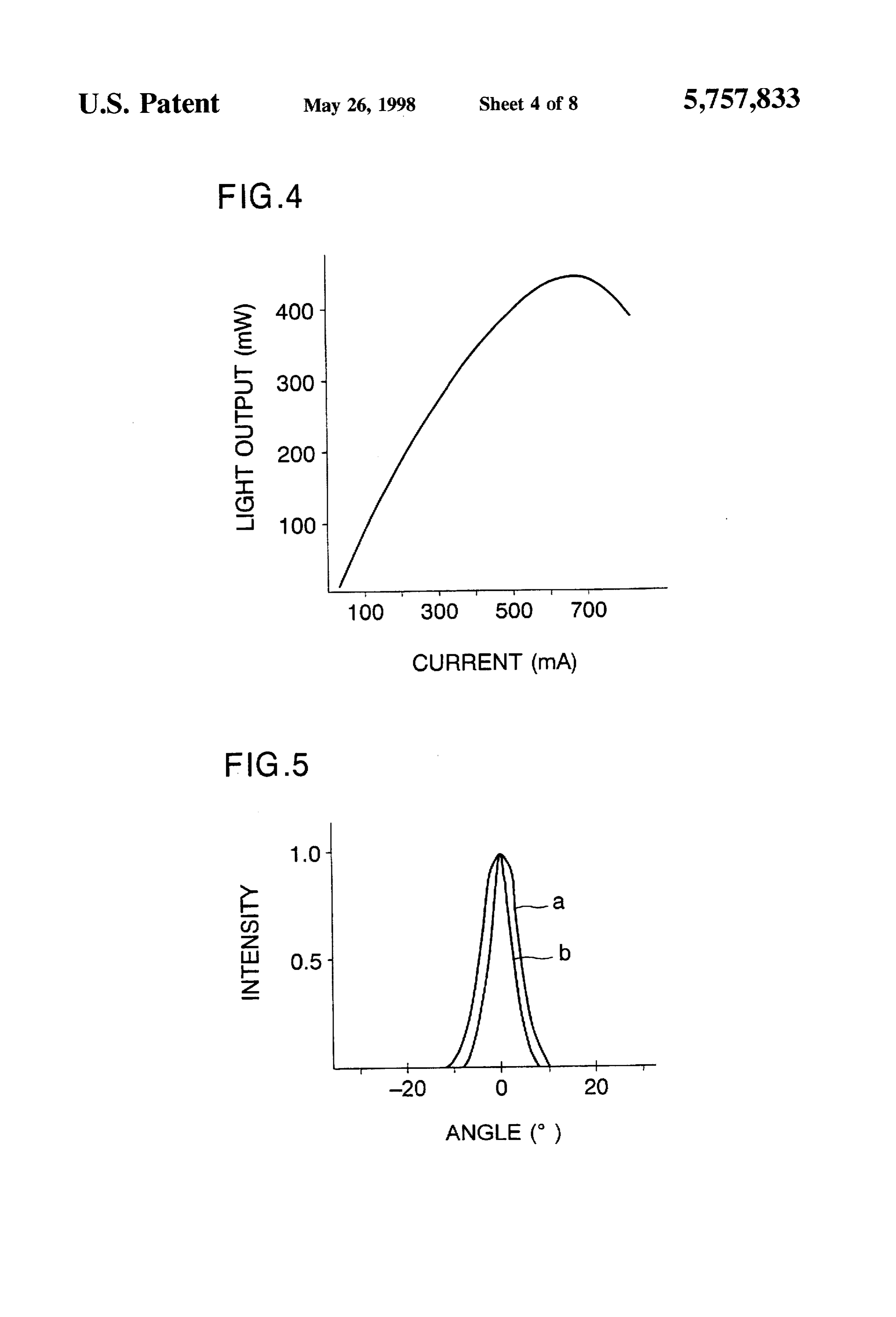
oscillation wavelength. In this process, a selective area 10 FIG. 4 is a graph showing a light output characteristic of growth mask is formed on a GaAs substrate except for a a semiconductor laser according to an embodiment of the region where a light emitting section is to be formed in such present invention;
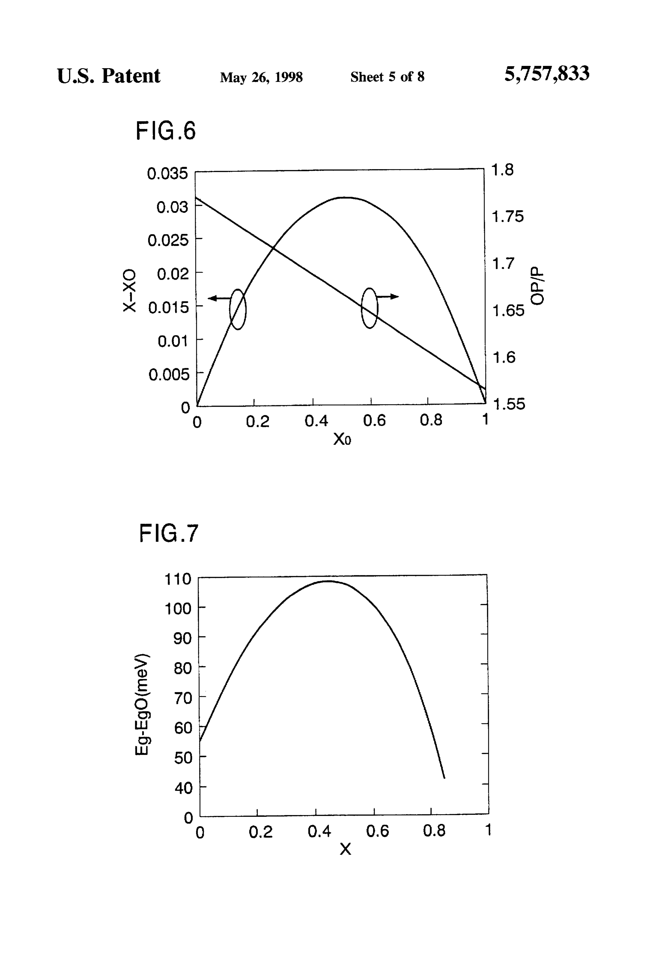
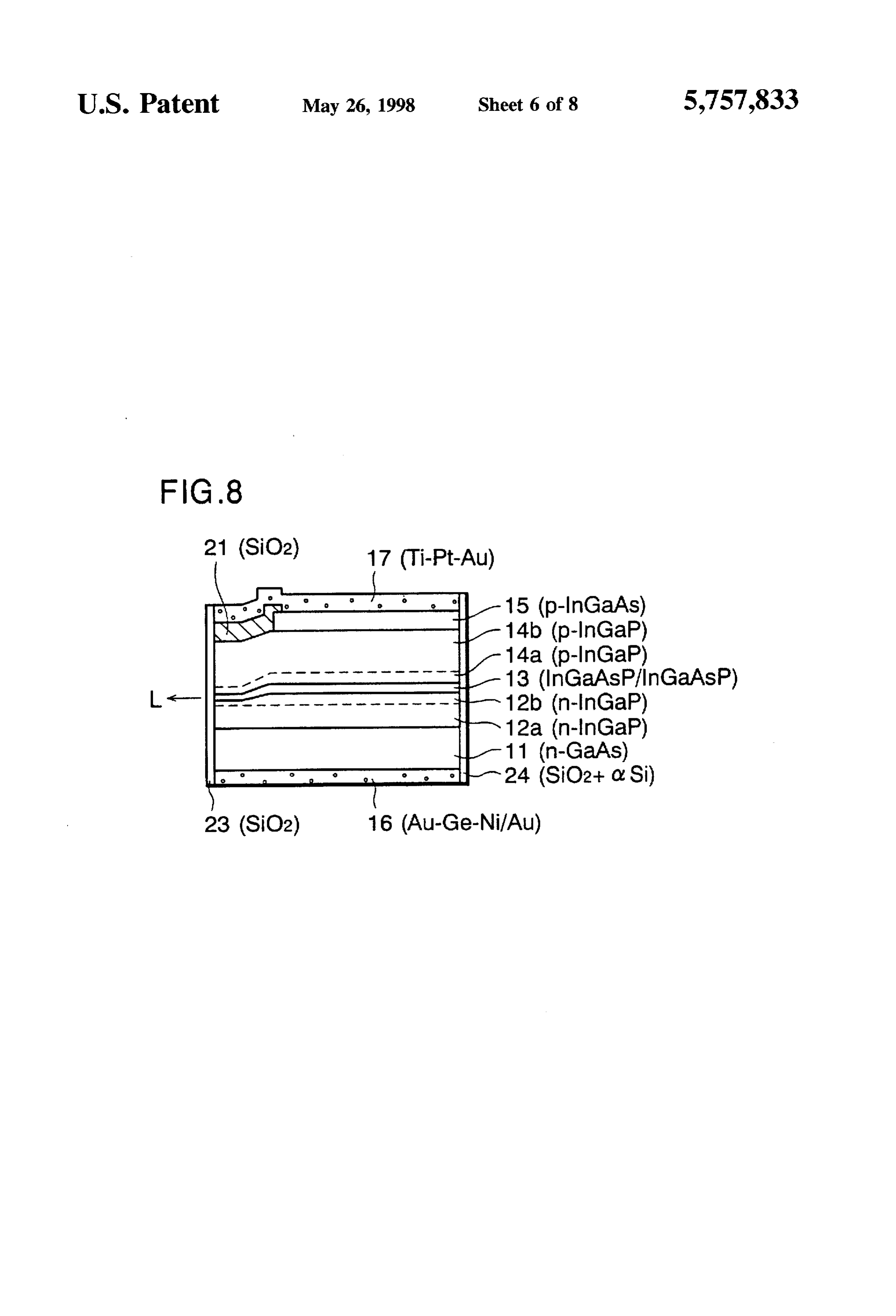
a manner that a region where a laser activation section is to FIG. 5 is a graph showing an intensity distribution char be formed is situated between segments of the selective area acteristic of a light beam emitted from the semiconductor growth mask, or the selective area growth mask is formed on 15 laser according to an embodiment of the present invention; the GaAs substrate in such a manner that the laser activation FIG. 6 is a graph illustrating advantageous effects of the section-forming region on the GaAs substrate has a prede semiconductor laser according to the present invention, or termined width free of the selective area growth mask, and more specifically, the difference in the proportion of Group that the light emitting section-forming region contiguous III elements between a mask region and a flat region grown with the laser activation section-forming region has a greater 20 by selective area growth, and the dependence of the film width free of the selective area growth mask than the thickness ratio on a Group III element proportion xo: predetermined width. Then, a multilayer semiconductor film FIG. 7 is a graph also illustrating an advantageous effect is formed on the GaAs substrate according to metal organic of the semiconductor laser according to the present chemical vapor deposition by using the selective area invention, or more specifically, the bandgap energy differ growth mask. 25 ences between the mask region and the flat region observed As a laser activation layer of the laser activation section when InCaAsP quantum well layers are formed with a and an optical waveguide layer of the light emitting section, Group III element proportion x varied; both formed on the GaAs substrate, an In-GaAsP FIG. 8 is a diagram showing a semiconductor laser layer is formed by selective area growth, where x indicates structure according to a preferred embodiment of the present the proportion of Group III elements satisfying the relation 30 invention;
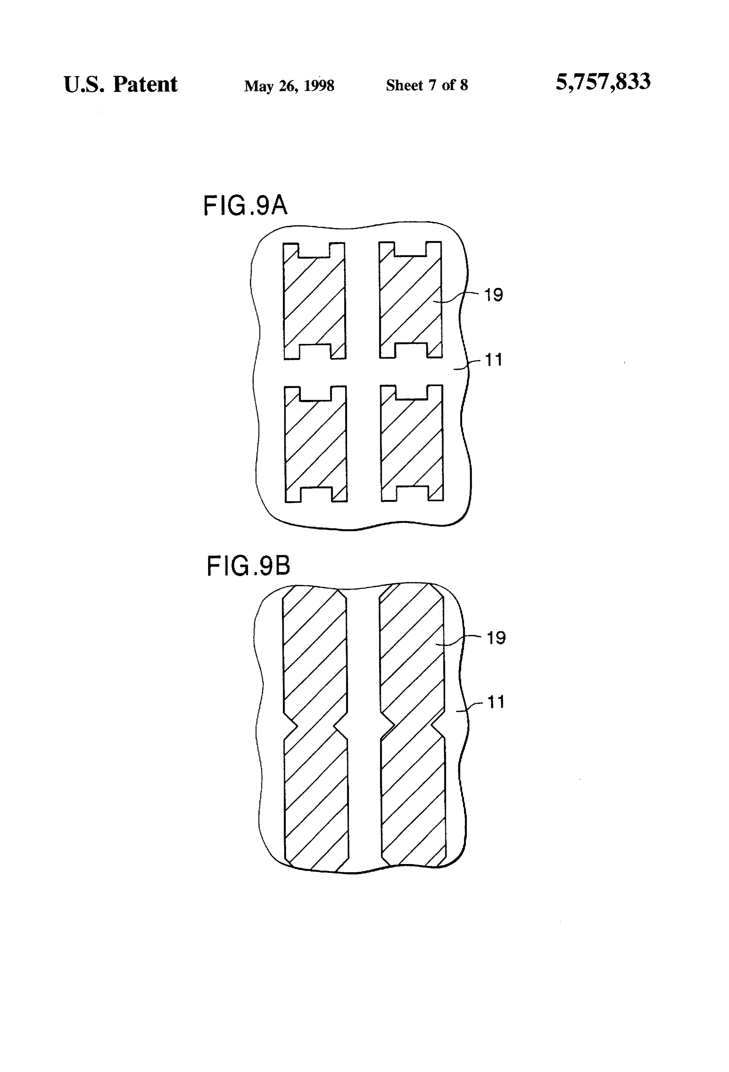
of 0<x<1, and y indicates the proportion of Group V FIG. 9A is a plan view showing a modification of the elements satisfying the relation of 0<y.<1. Preferably, the selective area growth mask pattern; proportion x of the Group III elements falls within the range FIG. 9B is a plan view showing another modification of
In this case, in order to set with precision the length of an 35 the selective area growth mask pattern; and optical waveguide which is given transparency with respect FIG. 10 is a sectional view showing a conventional to the laser oscillation wavelength, the distance between an structure of a semiconductor laser.
edge of the mask defining the laser activation section DETALED DESCRIPTION OF THE forming region and a light emitting end face should desir PREFERRED EMBODIMENTS ably be 100 pum or more. Also, to provide an effective difference of film thickness between the laser activation A semiconductor laser according to the present invention section and the light emitting section during the selective is obtained by the integrated formation of a laser activation area growth using the mask to thereby broaden the forbidden section and a light emitting section contiguous thereto, as a band of the optical waveguide of the light emitting section. multilayer film with a varying thickness on an n-type GaAs the proportion of the Group III elements, especially the 45 Substrate, for example, by means of a metal organic chemi content of indium (In) which can cause a large difference of cal vapor deposition process using a selective area growth selective growth rate dependent on the mask, should pref mask. A laser activation layer of the laser activation section erably be increased to such an extent that no characteristic and an optical waveguide layer of the light emitting section, deterioration takes place. in particular, are formed out of an InCaAsP layer with BRIEF DESCRIPTION OF THE DRAWTNGS different thicknesses. The oscillation wavelength of the laser activation layer is 0.8 to 1.1 um, preferably 6.98 m. Also,
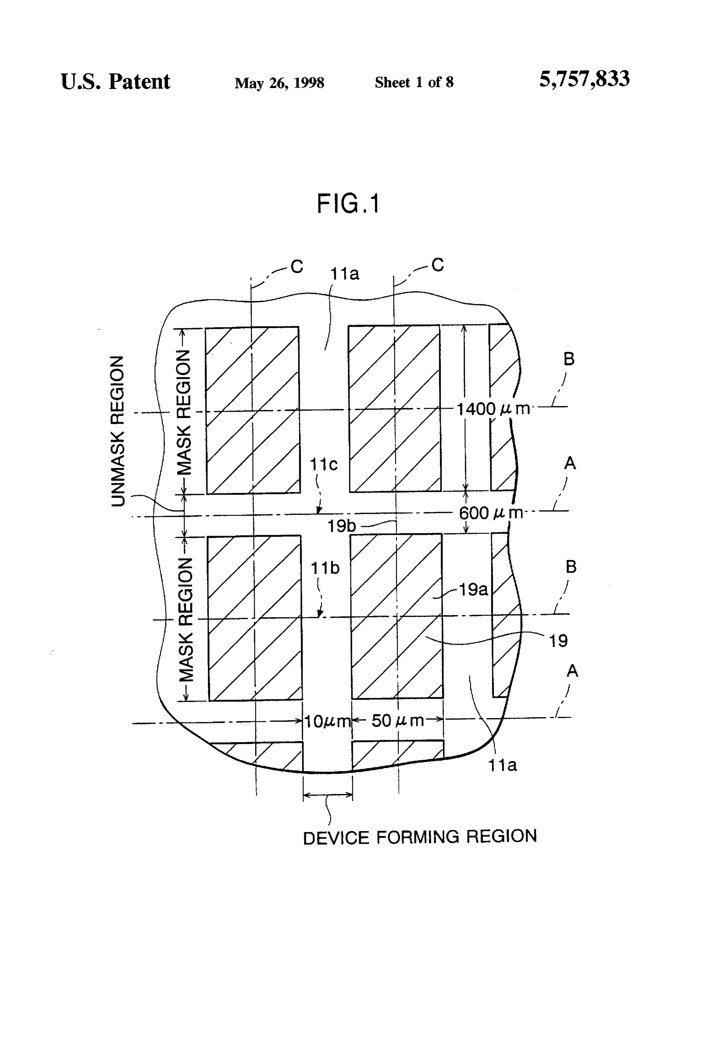
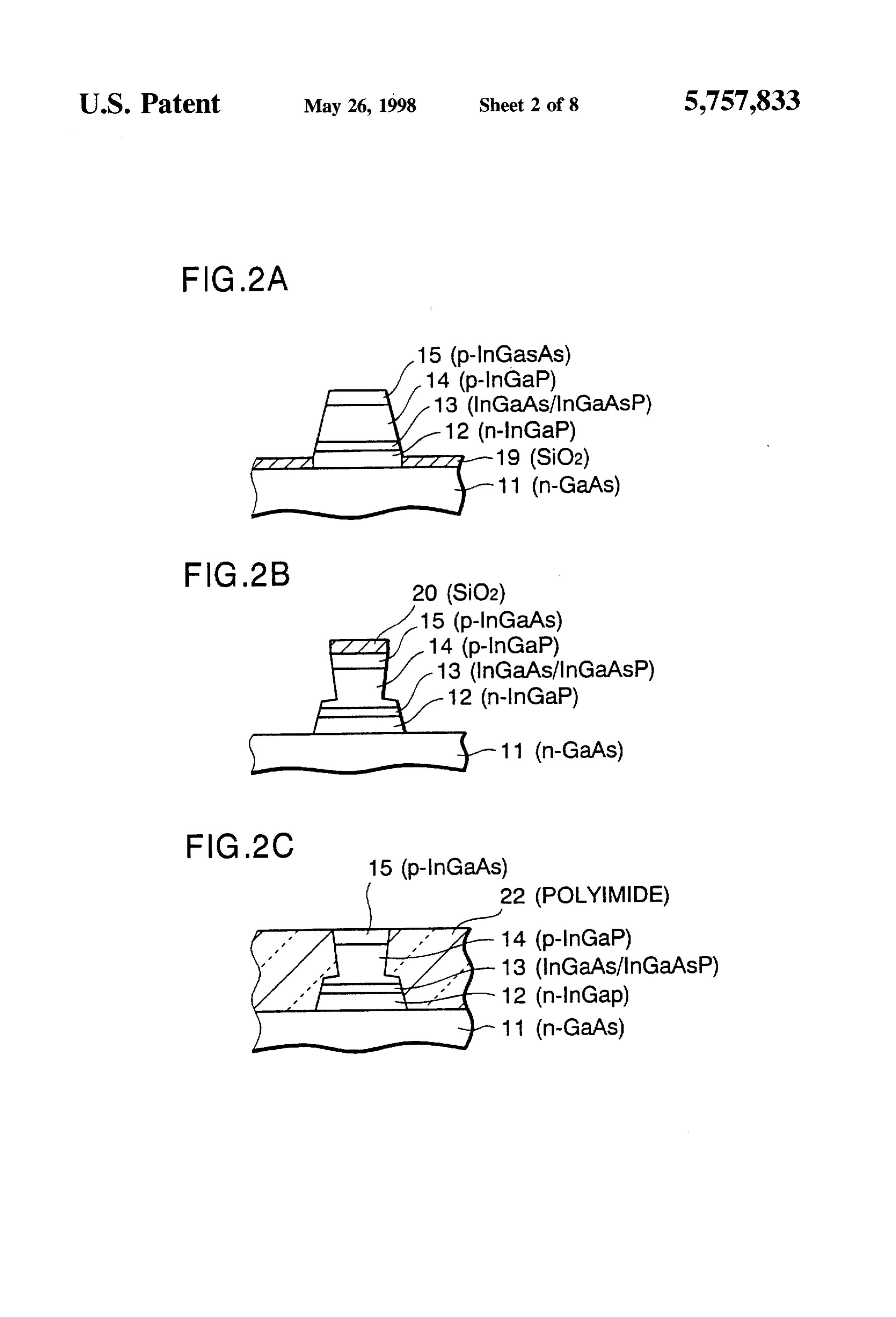
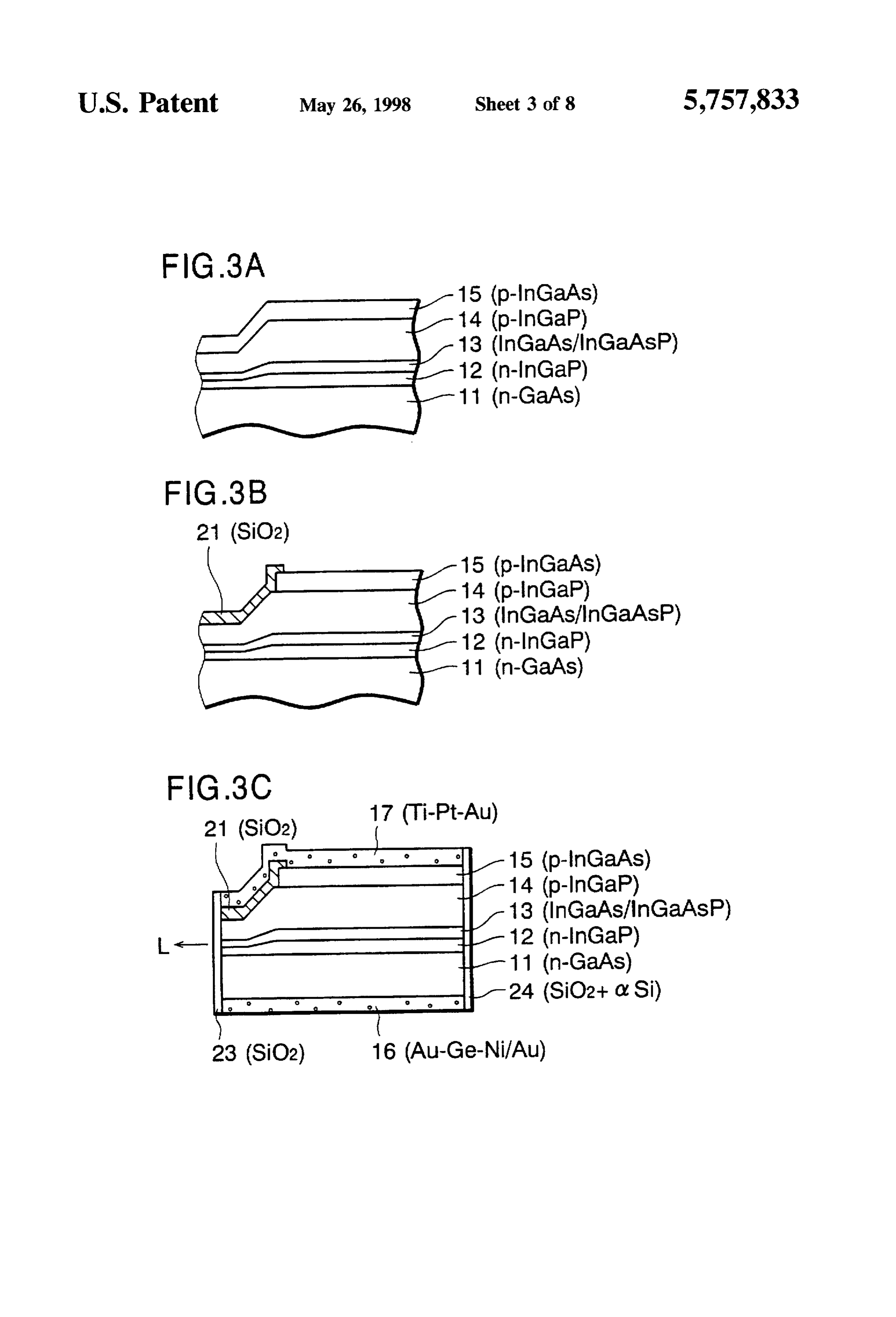
FIG. 1 is a plan view showing a pattern of a selective area the forbidden band of the optical waveguide layer is broad growth mask used in producing a semiconductor laser ened in order to impart transparency with respect to the laser according to one embodiment of the present invention; oscillation wavelength to the optical waveguide layer and FIG. 2A is a sectional view showing a structure of a 55 thereby permit increase of the output.
multilayer film grown on a GaAs substrate in section in a The semiconductor laser having the above-described width direction across mask segments, for illustrating a structure is produced by making the most use of the metal semiconductor laser production process according to one organic chemical vapor deposition process employing a embodiment of the present invention; selective area growth mask, as explained below. By suitably FIG. 2B is a sectional view showing a device structure selecting the composition of the multilayer semiconductor after the multilayer film is etched into an inverted-mesa film selectively grown on the GaAs substrate; moreover, it shape by using an etching mask; is possible to fabricate semiconductor lasers with high FIG. 2C is a sectional view showing a device structure reliability by a simple process. Also, the characteristics of after a current cutoff layer of a polyimide film is formed on the semiconductor laser can be improved. each side of the inverted mesa-shaped multilayer film; 65 FIG. 1 shows in plan view the pattern of a mask 19 for FIG. 3A is a sectional view of the multilayer film sec selective area growth used in producing a semiconductor tioned in a longitudinal direction along a device forming laser according to the present invention. The mask 19 is
Page 12
formed as an array of rectangular mask segments by sub ment layer and a strain quantum well layer. Then, a p-type jecting a SiO, film of about 100 nm thick, grown on an InGaPlayer as an upper cladding layer 14 is grown on the n-type GaAs substrate 11, for example, by plasma CVD laser activation layer 13, and finally a p-type InGaAs layer (chemical vapor deposition), to patterning by means of a is grown as a contact layer 15.
photolithography process using hydrofluoric acid as a buffer. In this case, the multilayer film is not formed on the The selective area growth mask 19 performs an important selective area growth mask 19. as shown in FIG. 2A. function in adjusting the thicknesses of an InCaPlayer and Further, as shown in FIG. 3A illustrating the device structure quantum well layer grown on the n-type GaAs substrate 11 sectioned in the longitudinal direction across the device by metal organic chemical vapor deposition (MOCVD). forming region 11a, the light emitting section-forming Especially, the mask 19 performs an important function in 10 region 11c, which is not situated between the rectangular growing the multilayer film with a varying thickness on mask segments 19b (in other words, situated between the regions of the GaAs substrate 11 where the laser activation unmasked section and the light emitting section are to be formed. that of the regions 19b). has a film thickness smaller than laser activation section-forming region 11b situ
Therefore, the mask 19 is formed so that it may have a ated between the rectangular mask segments 19b of the pattern defining the laser activation section-forming region 15 selective area growth mask 19, due to the inherent nature of and the light emitting section-forming region. the selective area growth process having dependence on the More specifically, the selective area growth mask 19 is selective area growth mask 19. Also, indium (In). which is formed as parallel mask segments 19a located along indi a Group III element, is actively introduced into the laser vidual regions of the GaAs substrate 11 where semiconduc activation section-forming region 11b, thus providing a tor lasers are to be formed in such a manner that each of 20 narrow forbidden band (small bandgap energy), whereas the multiple rows (stripes) of device forming regions 11a of 10 quantity of In introduced into the light emitting section pm wide, for example, is situated between the mask seg forming region 11c, which is not situated between the ments 19a. The rectangular mask segments 19a of the segments of the selective area growth mask 19, is restricted, selective area growth mask 19 separate adjacent ones of the so that its forbidden band is broad (the bandgap energy is device forming regions 11a from each other and each have 25 large).
a width of 50 m and a length of 1400 um. It should be noted With the multilayer film formed in the aforementioned in particular that the rectangular mask segments 19a are manner, the selective area growth mask 19 is removed using arranged such that laser activation section-forming regions hydrofluoric (laser activation regions) 11b, which are defined in the formed over acid as a buffer, and then a SiO film is again stripe-like device forming regions 11a, are situated between CVD process.theSubsequently, entire surface of the structure by a plasma the SiO film is partly removed the mask segments 19a. An unmasked region 19b of 600 um by photolithography using hydrofluoric long is provided on each side of a light emitting section that the SiO film is left only on the acid as a buffer such forming region 11c contiguous to the laser activation sec obtain an etching mask 20, as shown in FIG. 2B.layer contact 15 to Using the tion.
In the case where two semiconductor lasers are to be 35 etching mask 20, the multilayer film is partly etched from formed on each laser activation section-forming region 11b the upper contact layer 15 down to an intermediate portion of the cladding layer 14, as shown in FIG. 2B. so that the with their laser activation sections laid out back to back (facing in opposite directions), for example, the length of multilayer film formed on each row of the device forming each rectangular mask segment 19a (laser device region and the light(the regions 11a laser activation section-forming regions 11b emitting section-forming region 11c) has the 11b) is set to a value twice the longitudinal length (laser shape of an inverted mesa. Tartaric acid is used as an etchant activation region length) of the laser activation section of the for semiconductor laser to be formed. The longitudinal length of as anetching etchant the InGaAs layer, and hydrochloric acid is used for etching the InGaPlayer.
the unmasked region 19b is set to a value twice or more the length of the light emitting section (optical waveguide) forming region 11c ismask
Then, the etching 20 on the light emitting section removed, and using the etching mask contiguous to the laser activation section. Shortly, in the 45 remaining on the laser activation illustrated example, semiconductor lasers which each have a 20 11b, the contact layer 15 on the section-forming region light emitting section laser activation region length of 700 um and in which the forming region 11c is removed, followed by the removal of light emitting section contiguous to the laser activation the remaining etching mask 20. Subsequently, as shown in region has a waveguide length of 300 um are continuously FIG. 3B, a SiO film is formed only on the region (light formed on each row of the device forming regions 11a 50 emitting section-forming region 11c) from which the contact having a width of 10 um, and to this end, the rectangular layer 15 has been removed, thereby obtaining a current mask segments 19b each having a width of 50 um and a length of 1400 m are arrayed with a longitudinal space of blocking layer 21. The current blocking layer 21 may be 600 m such that the individual device forming regions 11a formed of the by first forming an SiO film over the entire surface multilayer film and then etching the SiO, film in such are situated between the mask segments 19b. 55 a manner that the film is left only on the region from which
After the selective area growth mask 19 having the the contact layer 15 has been removed. aforementioned pattern is formed on the n-type GaAs sub strate 11, semiconductor layers mentioned below are suc A polyimide film, which serves as a current cutoff layer cessively and selectively grown on the n-type GaAs sub 22, is formed on each side of the inverted mesa-shaped strate 11 according to, for example, a metal organic chemical multilayer film, as shown in FIG. 2C. vapor deposition (MOCVD) process under reduced After the current blocking layer 21 and the current cutoff pressure. by using the mask 19. Specifically, as shown in layer 22 are formed in the above manner, the back surface FIG. 2A which illustrates the device structure sectioned in or underside of the n-type GaAs substrate 11 is polished such the width direction across mask segments, an n-type InGaP that the thickness of the substrate is reduced to about 100 layer is first grown as a lower cladding layer 12, and an 65 um, an Au-Ge-Ni/Au layer as a negative electrode 16, for InGaAs/InGaAsP layer, for example, is grown on the layer example, is deposited on the back surface of the GaAs 12 as a laser activation layer 13 including a light confine substrate 11, and a Ti-Pt-Aulayer as a positive electrode 17
Page 13
is deposited on the contact layer 15 and the current blocking is prominent in the case where a Group III material, espe layer 21, as shown in FIG. 3C. cially indium (In), is used, and is relatively low where Subsequently, the GaAs substrate 11 with the multilayer gallium (Ga) is used. Accordingly, with a conventional film formed thereon as described above is cleaved at the semiconductor laser having an ordinary oscillation wave center (lines A in FIG. 1) of each unmasked region 19b length of 1 in or thereabouts and using InGaAs (x=0.8 situated between longitudinally adjacent segments of the to 0.9) as its strain quantum well layer, a sufficiently high selective area growth mask 19, and at the longitudinal center selective area growth effect sometimes cannot be expected (lines B in FIG. 1) of the selective area growth mask 19, to because of a small In content. However, if the In content, for thereby obtain laser diode bars whose cleaved faces serve as example, is increased in order to enhance the selective area a light emitting surface and a light reflecting surface, respec 10 growth effect, another problem arises in that large strain is tively. Then, as shown in FIG. 3C, a SiO, film as a caused when the laser oscillation wavelength is set to a low-reflectivity film 23 having a reflectivity of 5% is formed desired value.
on the surface (light emitting surface) cleaved along line A, and a high-reflectivity film 24 with a reflectivity of 95%, for Therefore, in the semiconductor laser according to the example, a laminate of a SiO2 film and an amorphous silicon 15 present invention, InGaAsP- (x=0.7; y=0.65), for film, is formed on the surface (light reflecting surface) example, is used especially for the strain quantum well layer (laser activation layer). Specifically, where the selective area cleaved along line B.
Each of the laser diode bars is then cut at the boundary growth um, the mask 19 of 50 um wide is formed with a gap of 10 proportion x of the Group III element composition between adjacent semiconductor lasers in the width grown on the region (laser activation section-forming direction, that is, at the center (lines C in FIG. 1) of the region, hereinafter referred to as "mask region”) situated selective area growth mask 19, to obtain individual semi between the segments of the mask 19 and the proportion xo conductor lasers, whereby semiconductor lasers each pro vided with a light emitting section having transparency with of the Group II element composition grown on the region (light emitting section-forming region. hereinafter referred respect to the laser oscillation wavelength are finally obtained. The light emitting direction is indicated by arrow 25 to as "flat region") where no mask 19 is formed have a difference x-xo as shown in FIG. 6. Also, the dependence of
In the semiconductor laser fabricated by the aforemen the film thickness ratio d/d on the proportion x of the Group III element composition is shown in FIG. 6.
tioned steps, the optical waveguide layer of the light emit ting section has a small In content and thus has a broad Group IIIcase
In the of the aforementioned In-GaAsP the forbidden band (large bandgap energy), as compared with 30 and in FIG.composition x can be expressed as Ga/(Ga--In). the laser activation layer of the laser activation section, and the leftward direction along istheindicated 6, the In content so as to increase in horizontal axis. Therefore, therefore, the waveguide layer exhibits transparency with respect to the laser oscillation wavelength. In addition, since FIG. 6 reveals that the higher the In content, the greater the the upper surface of the waveguide layer is covered with the film thickness ratio becomes, and that the film thickness current blocking layer 21, resistance to catastrophic optical 35 difference increases due to the masking effect achieved by damage (COD) is large, making it possible to increase the the selective area growth. It can also be seen that the light output. difference (x-xo) in proportion between the compositions is For example, in a semiconductor laser with an oscillation S2C.greatest where the In and Ga contents are almost the the wavelength of 0.98 um produced following the aforemen tioned steps, the optical waveguide at the light emitting Based on these findings, quantum wells each having an section had a considerably large forbidden band of about In-GaAsP layer were formed with the proportion x of 0.88 um. Consequently, even when an excitation current of the Group III element composition varied, and they showed 600 mA or more was passed through the semiconductor laser differences Eg-Ego of the bandgap energy between the mask to obtain a light output of 400 mW or more, no catastrophic region and the flat region as shown in FIG. 7. In this case, optical damage was observed, as seen from the light output 45 the composition of the Group V elements was selected so characteristic shown in FIG. 4, for example. By contrast, a that the mask region had a film thickness of 9 nm and that semiconductor laser produced by conventional techniques is the laser oscillation wavelength (light emission wavelength) destroyed due to catastrophic optical damage (COD) when was 0.97 m.
a current is passed to obtain a light output as low as about Since the bandgap of the quantum well layer is deter 200 mW. 50 mined by its film thickness and composition, the amount of Further, in the semiconductor laser with an oscillation change in the bandgap is affected by both the difference in wavelength of 0.98 m fabricated in the above-described proportion between the aforementioned compositions and manner, the optical waveguide region with a large forbidden the film thickness difference shown in FIG. 6. Accordingly, band has a length of 300 m or more (the distance between the amount of change in the bandgap (forbidden band) longitudinally adjacent segments of the selective area 55 attained by the selective area growth using the mask 19 growth mask 19 is 600 m). and therefore, the spot size can greatly depends on the Group III element composition of the be enlarged. Also, light emitted from the light emitting quantum well layer.
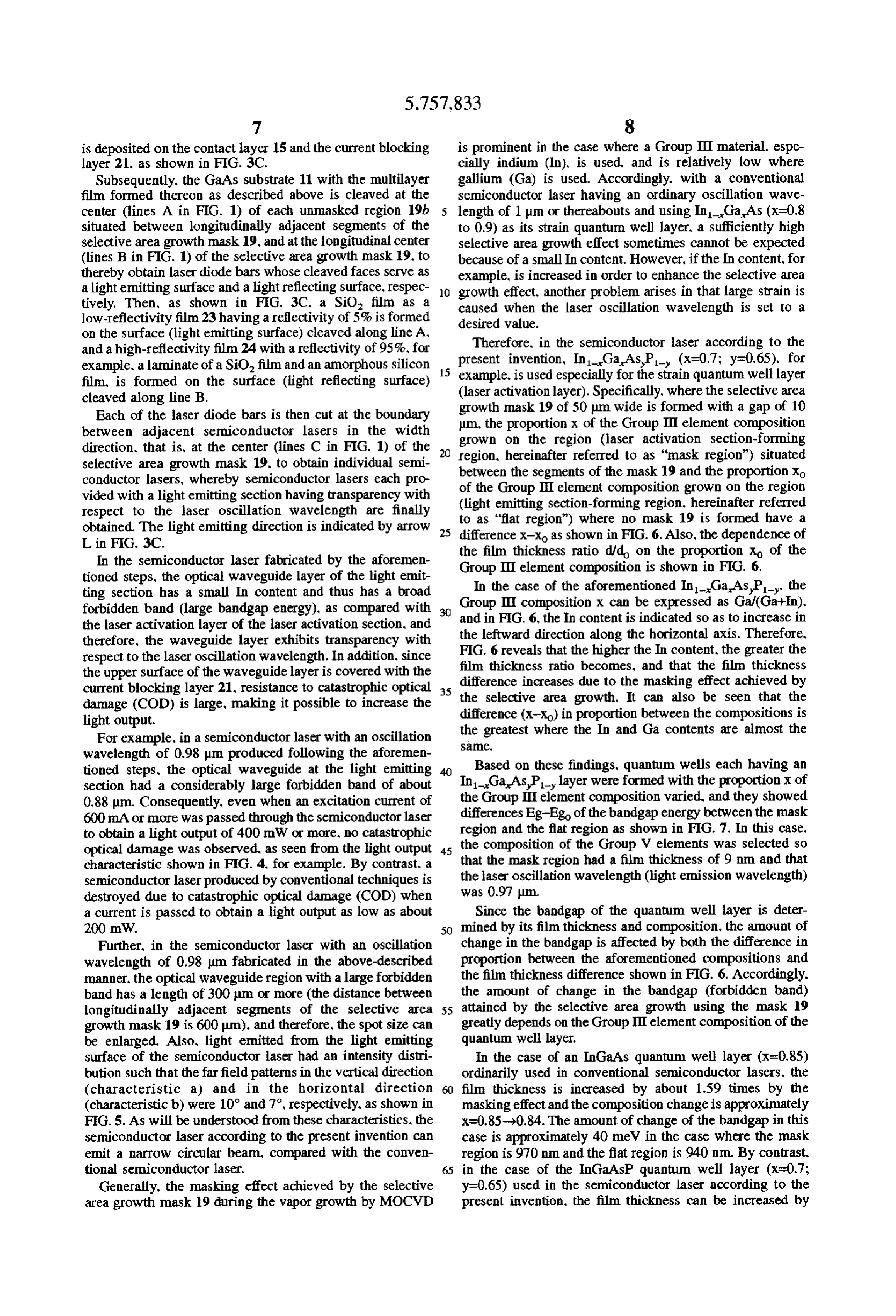
surface of the semiconductor laser had an intensity distri In the case of an InCaAs quantum well layer (x=0.85) bution such that the farfield patterns in the vertical direction ordinarily used in conventional semiconductor lasers, the (characteristic a) and in the horizontal direction film thickness is increased by about 1.59 times by the (characteristic b) were 10° and 7, respectively, as shown in masking effect and the composition change is approximately FIG. 5. As will be understood from these characteristics, the x=0.85-90.84. The amount of change of the bandgap in this semiconductor laser according to the present invention can case is approximately 40 meV in the case where the mask emit a narrow circular beam, compared with the conven region is 970 nm and the flat region is 940 nm. By contrast, tional semiconductor laser. 65 in the case of the InGaAsP quantum well layer (x=0.7; Generally, the masking effect achieved by the selective y=0.65) used in the semiconductor laser according to the area growth mask 19 during the vapor growth by MOCVD present invention, the film thickness can be increased by
Page 14
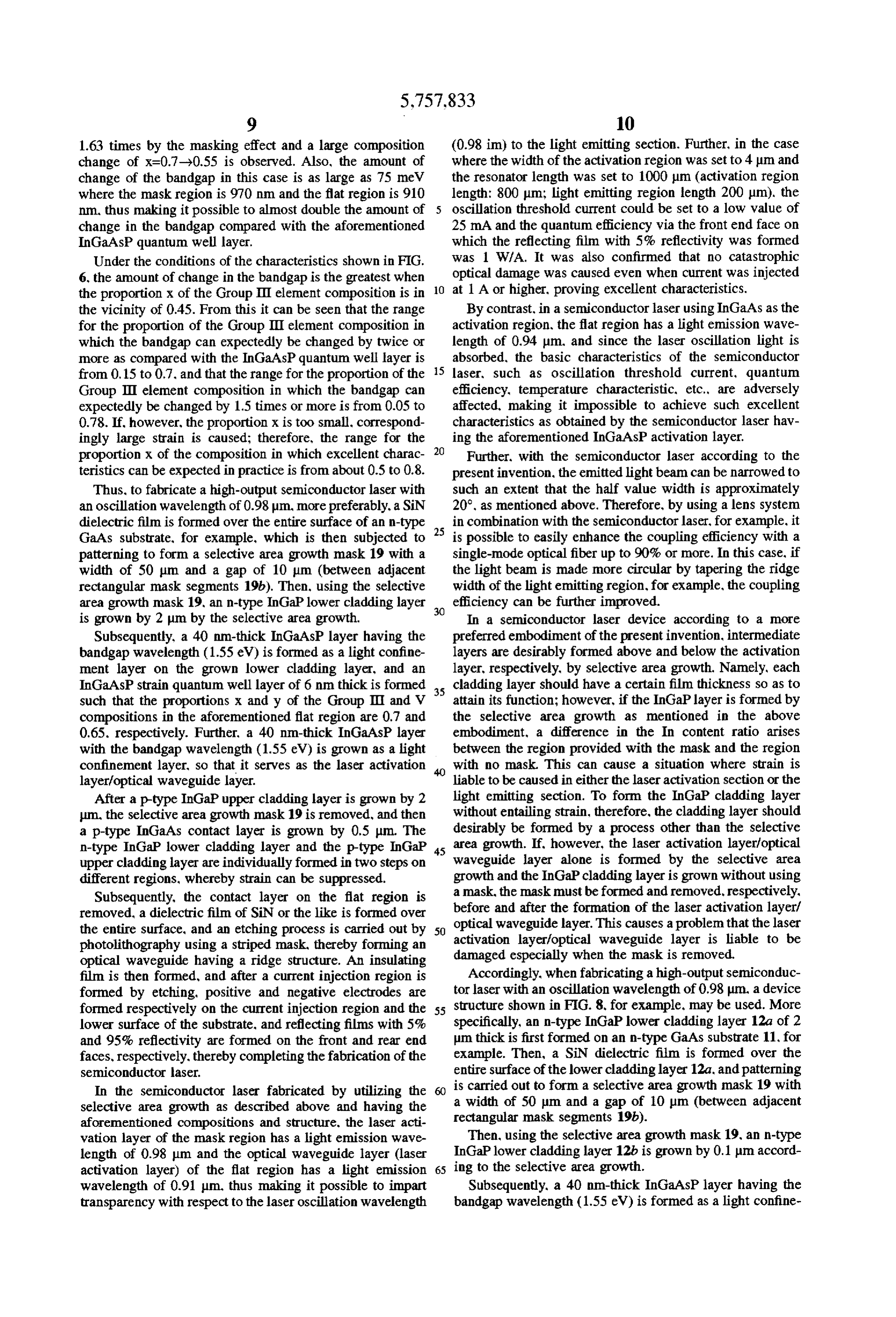
1.63 times by the masking effect and a large composition (0.98 im) to the light emitting section. Further, in the case change of x=0.7->0.55 is observed. Also, the amount of where the width of the activation region was set to 4 um and change of the bandgap in this case is as large as 75 meV the resonator length was set to 1000 um (activation region where the mask region is 970 nm and the flat region is 910 length: 800 pm; light emitting region length 200 pm), the nm, thus making it possible to almost double the amount of 5 oscillation threshold current could be set to a low value of change in the bandgap compared with the aforementioned 25 mA and the quantum efficiency via the front end face on InGaAsP quantum well layer. which the reflecting film with 5% reflectivity was formed Under the conditions of the characteristics shown in FIG. was 1 W/A. It was also confirmed that no catastrophic 6, the amount of change in the bandgap is the greatest when optical damage was caused even when current was injected the proportion x of the Group III element composition is in 10 at 1 A or higher, proving excellent characteristics. the vicinity of 0.45. From this it can be seen that the range By contrast, in a semiconductor laser using InCaAs as the for the proportion of the Group III element composition in activation region, the flat region has a light emission wave which the bandgap can expectedly be changed by twice or length of 0.94 um, and since the laser oscillation light is more as compared with the InGaAsP quantum well layer is absorbed, the basic characteristics of the semiconductor from 0.15 to 0.7. and that the range for the proportion of the 15 laser, such as oscillation threshold current, quantum Group III element composition in which the bandgap can efficiency, temperature characteristic, etc., are adversely expectedly be changed by 1.5 times or more is from 0.05 to affected, making it impossible to achieve such excellent 0.78. If, however, the proportion x is too small, correspond characteristics as obtained by the semiconductor laser hav ingly large strain is caused; therefore, the range for the ing the aforementioned InGaAsP activation layer. proportion X of the composition in which excellent charac Further, with the semiconductor laser according to the teristics can be expected in practice is from about 0.5 to 0.8. present invention, the emitted light beam can be narrowed to Thus, to fabricate a high-output semiconductor laser with such an extent that the half value width is approximately an oscillation wavelength of 0.98 um, more preferably, a SiN 20°, as mentioned above. Therefore, by using a lens system dielectric film is formed over the entire surface of an n-type in combination with the semiconductor laser, for example, it GaAs substrate, for example, which is then subjected to 25 is possible to easily enhance the coupling efficiency with a patterning to form a selective area growth mask 19 with a single-mode optical fiber up to 90% or more. In this case, if width of 50 m and a gap of 10 m (between adjacent the light beam is made more circular by tapering the ridge rectangular mask segments 19b). Then, using the selective width of the light emitting region, for example, the coupling area growth mask 19, an n-type InGaP lower cladding layer 30 efficiency can be further improved. is grown by 2 um by the selective area growth. In a semiconductor laser device according to a more Subsequently, a 40 nm-thick InGaAsP layer having the preferred embodiment of the present invention, intermediate bandgap wavelength (1.55 eV) is formed as a light confine layers are desirably formed above and below the activation ment layer on the grown lower cladding layer, and an layer, respectively, by selective area growth. Namely, each InGaAsP strain quantum well layer of 6nm thick is formed 35 cladding layer should have a certain film thickness so as to such that the proportions x and y of the Group III and V attain its function; however, if the InGaPlayer is formed by compositions in the aforementioned flat region are 0.7 and the selective area growth as mentioned in the above 0.65. respectively. Further, a 40 nm-thick InGaAsP layer embodiment, a difference in the In content ratio arises with the bandgap wavelength (1.55 eV) is grown as a light between the region provided with the mask and the region confinement layer, so that it serves as the laser activation with no mask. This can cause a situation where strain is layer/optical waveguide layer. liable to be caused in either the laseractivation section or the After a p-type InGap upper cladding layer is grown by 2 light emitting section. To form the InGaP cladding layer im, the selective area growth mask 19 is removed, and then without entailing strain, therefore, the cladding layer should a p-type InGaAs contact layer is grown by 0.5 m. The desirably be formed by a process other than the selective n-type InGaP lower cladding layer and the p-type InGaP 45 area growth. If, however, the laser activation layer/optical upper cladding layer are individually formed in two steps on waveguide layer alone is formed by the selective area different regions, whereby strain can be suppressed. growth and the InGap cladding layer is grown without using Subsequently, the contact layer on the flat region is a mask, the mask must be formed and removed, respectively, removed, a dielectric film of SiN or the like is formed over before and after the formation of the laser activation layer/ the entire surface, and an etching process is carried out by 50 optical waveguide layer. This causes a problem that the laser photolithography using a striped mask, thereby forming an activation layer/optical waveguide layer is liable to be optical waveguide having a ridge structure. An insulating damaged especially when the mask is removed. film is then formed, and after a current injection region is Accordingly, when fabricating a high-output semiconduc formed by etching, positive and negative electrodes are tor laser with an oscillation wavelength of 0.98 um, a device formed respectively on the current injection region and the 55 structure shown in FIG. 8, for example, may be used. More lower surface of the substrate, and reflecting films with 5% specifically, an n-type InGap lower cladding layer 12a of 2 and 95% reflectivity are formed on the front and rear end um thick is first formed on an n-type GaAs substrate 11, for faces, respectively, thereby completing the fabrication of the example. Then, a SiN dielectric film is formed over the semiconductor laser. entire surface of the lower cladding layer 12a, and patterning In the semiconductor laser fabricated by utilizing the isa widthcarried out to form a selective area growth mask 19 with of 50 m and a gap of 10 pum (between adjacent selective area growth as described above and having the aforementioned compositions and structure, the laser acti rectangular mask segments 19b).
vation layer of the mask region has a light emission wave Then, using the selective area growth mask 19, an n-type length of 0.98 m and the optical waveguide layer (laser InGaPlower cladding layer 12b is grown by 0.1 um accord activation layer) of the flat region has a light emission 65 ing to the selective area growth.
wavelength of 0.91 m, thus making it possible to impart Subsequently, a 40 nm-thick InGaAsP layer having the transparency with respect to the laser oscillation wavelength bandgap wavelength (1.55 eV) is formed as a light confine
Page 15
ment layer on the grown lower cladding layer, and an employed instead. Also, in the embodiment, the gap InGaAsP strain quantum well layer of 6nm thick is formed (spacing) between mask segments 19 is set to 10 pum, and the such that the proportions x and y of the Group III and V activation layer formed along the gap by the selective area compositions in the aforementioned flat region are 0.7 and growth is etched into an inverted-mesa shape to obtain a 0.65, respectively. Further, a 40 nm-thick InCaAsP layer 5 laser activation region. Alternatively, the gap width may of with the bandgap wavelength (1.55 eV) is grown as a light the course be set to a value almost equal to the actual width of confinement layer, so that it serves as the laser activation layerlaser activation layer so that the entirety of the activation formed by the selective area growth may be used as the layer/optical waveguide layer.
Then, a p-type InGap upper cladding layer 14a is grown embodiment, the region.
laser activation Further, although in the above activation layer is formed as a single by 0.1 m on the InGaAsP layer. 10 quantum well layer, it may have a multilayer quantum well
After the selective area growth mask 19 is removed, a structure having two or more layers.
p-type InGap upper cladding layer 14b is grown by 2 um Furthermore, instead of using InGaAsP as the light con over the entire surface, and a p-type InGaAs contact layer 15 finement layer. GaAsP may be used, and also in this case is grown by 0.5 um on the upper cladding layer 14b. similar effects can be obtained. The activation layer of the Subsequently, the contact layer on the flat region is 15 embodiment involves a compression strain of about +1.5%; removed, a dielectric film of SiN or the like is formed over therefore, if IngaAsP or GaAsP having extension strain is the entire surface, and an etching process is carried out by used so that the strain of the activation layer is compensated photolithography using a striped mask, thereby forming an for, the crystallization performance is enhanced, improving optical waveguide having a ridge structure. An insulating the characteristics.
film is then formed, and after a current injection region is 20 Also, instead of InCap, AlGaAs may of course be used for formed by etching, positive and negative electrodes 17 and the cladding layer. Further, if a thin AlAs layer is formed in 16 are formed respectively on the current injection region the cladding layer and after the formation of ridges, the light and the lower surface of the substrate, and reflecting films 13 emitting section is subjected to selective oxidation, then the and 24 with 5% and 95% reflectivity are formed on the front current blocking with respect to the light emitting section and rear end faces. respectively, thereby completing the 25 can be ensured with higher reliability. fabrication of the semiconductor laser. Further, by tapering the ridge width of the light emitting As described above, the n-type InGap lower cladding section to optimize the selective oxidation condition. it is layer 12a, 12b and the p-type InGap upper cladding layer possible to cause a current corresponding to the distance 14a. 14b are individually formed in two steps, whereby 30 from the activation region to flow only to the light emitting strain of the cladding layers can be prevented. Especially, section in the vicinity of the activation region. Specifically, after forming the thick n-type InGap lower cladding layer according to selective area growth techniques generally 12a which forms a main part of the lower cladding layer, the employed, a transition region is produced between the mask n-type InGap lower cladding layer 12b, the laser activation region and the flat region, and therefore, distance-dependent layer/optical waveguide layer 13, and the p-type InGap 35 light absorption occurs at the light emitting section in the upper cladding layer 14a are formed by a selective area vicinity of the activation region, causing the possibility of growth process using the selective area growth mask 19. the device characteristics being deteriorated. With the struc Then, the selective area growth mask 19 is removed by ture described above, such inconveniences can be elimi etching, and the thick p-type InGap upper cladding layer nated.
14b, which constitutes a main part of the upper cladding According to the present invention, therefore, not only the layer, is formed. It is therefore possible to form cladding manufacturing process is simplified but also a semiconduc layers of which the characteristics are stable. tor laser having improved characteristics and capable of high If, on the other hand, the laser activation layer/optical output can be provided. In addition, since the light emitting waveguide layer 13 alone is formed by a selective area section has transparency with respect to the laser oscillation growth process using the selective area growth mask 19, the 45 wavelength, the spread angle of the emitted light can be laser activation layerdoptical waveguide layer 13 may pos controlled so as to obtain a nearly circular light beam having sibly be roughened and thus its characteristics are deterio a sufficiently narrow far field pattern, whereby the coupling rated when the selective area growth mask 19 is removed by efficiency with an optical fiber and other characteristics can etching after the growth of the laser activation layer/optical be enhanced.
waveguide layer 13. Also in view of this, the individual 50 In particular, since the activation layer of InGaAsP is cladding layers should preferably beformed in two steps, as formed on the GaAs substrate, it is possible to fabricate with mentioned above, to ensure the quality of the laser activation high reliability and ease high-output semiconductor lasers layerfoptical waveguide layer 13. with an oscillation wavelength of 0.8 to 1.1 pm, which The present invention is not limited to the embodiment wavelength is required when the device is used as an optical described above. For example, the selective area growth 55 repeater.
mask 19 may have patterns as shown in FIGS. 9A and 9B. What is claimed is:
In brief, since the rate of vapor growth of films (film 1. A semiconductor laser with a multilayer structure thicknesses) on the mask region and on the flat region varies formed on a GaAs substrate, comprising: depending on the mask width and the width of a gap between a laser activation section and a light emitting section mask segments, the mask width (width of the gap between simultaneously formed by a metal organic chemical mask segments) at the laser device-forming region and the vapor deposition process using a selective area growth light emitting section-forming region should only be mask to produce an effect that said laser activation changed in accordance with the required film thicknesses section and said light emitting section differ in film etc. thickness,
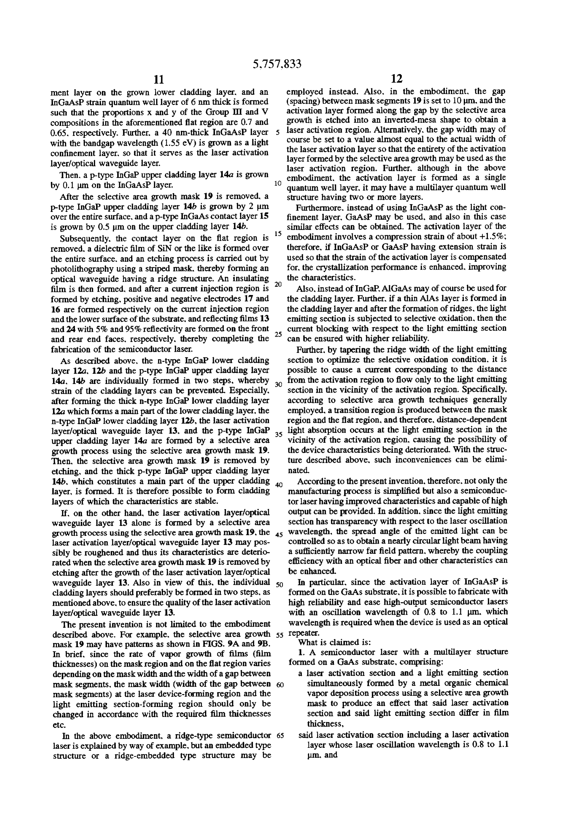
In the above embodiment, a ridge-type semiconductor 65 said laser activation section including a laser activation laser is explained by way of example, but an embedded type layer whose laser oscillation wavelength is 0.8 to 1.1 structure or a ridge-embedded type structure may be um, and
Page 16
said light emitting section including an optical waveguide section and an optical waveguide layer of the light emitting layer, the optical waveguide layer having a broad section, are obtained by growing an InGaAsP layer. forbidden band compared with the laser activation layer where x indicates a proportion of Group III elements satis and having transparency with respect to the laser oscil fying a relation of 0<x<1, and y indicates a proportion of lation wavelength. Group V elements satisfying a relation of 0<y<1. 2. The semiconductor laser according to claim 1, wherein 6. A process of producing a semiconductor laser of the laser activation layer of said laser activation section and multilayer structure provided with a light emitting section the optical waveguide layer of said light emitting section having transparency with respect to a laser oscillation wave each comprise an InGaAsP layer, where x indicates length of 0.8 to 1.1 um, comprising: a proportion of Group III elements satisfying a relation of 10 forming selective area growth masks on a GaAs substrate 0<x<1, and y indicates a proportion of Group V elements in such a manner that a laser activation section-forming satisfying a relation of 0<y(1. region on the GaAs substrate where a laser activation 3. The semiconductor laser according to claim 2, wherein section is to be formed has a predetermined width free the proportion x of the Group DII elements in the In of the selective area growth masks, and such that a light GaAsP layer falls within a range of 0.5 to 0.8. 15 emitting section-forming region contiguous with the 4. A process of producing a semiconductor laser of laser activation section-forming region has a greater multilayer structure provided with a light emitting section width free of the selective area growth masks than the having transparency with respect to a laser oscillation wave predetermined width; and length of 0.8 to 1.1 um, comprising: forming multiple semiconductor layers on said laser acti forming a pair of selective area growth masks on a GaAs vation section-forming region of the GaAs substrate by substrate except for a region where a light emitting metal organic chemical vapor deposition by using the section is to be formed in such a manner that a region selective area growth masks, said multiple semicon where a laser activation section is to be formed is ductor layers comprising a laser activation layer of the situated between said pair of selective area growth 25 laser activation section having a laser oscillation wave masks; and length band of 0.8 to 1.1 um, and wherein said laser forming multiple semiconductor layers on said laser acti activation section and said light emitting section are vation section-forming region of the GaAs substrate by simultaneously formed by said metal organic chemical metal organic chemical vapor deposition by using the vapor deposition process.
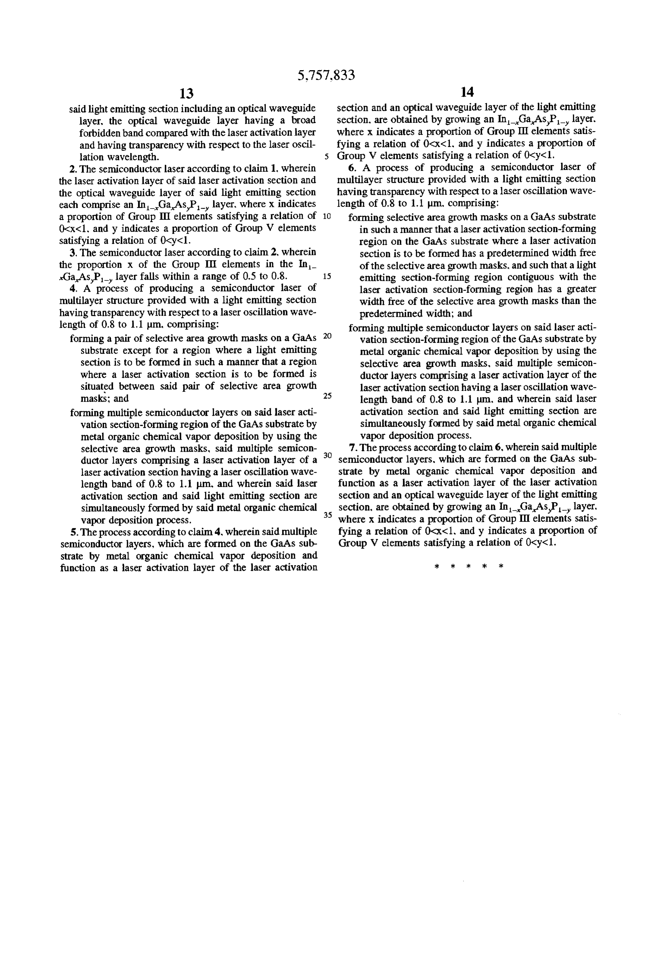
selective area growth masks, said multiple semicon 30 7. The process according to claim 6, wherein said multiple ductor layers comprising a laser activation layer of a semiconductor layers, which are formed on the GaAs sub laser activation section having a laser oscillation wave strate by metal organic chemical vapor deposition and length band of 0.8 to 1.1 m, and wherein said laser function as a laser activation layer of the laser activation activation section and said light emitting section are section and an optical waveguide layer of the light emitting simultaneously formed by said metal organic chemical 35 section, are obtained by growing an InGaAsP layer. vapor deposition process. where x indicates a proportion of Group III elements satis 5. The process according to claim 4, wherein said multiple fying a relation of 0<x<1, and y indicates a proportion of semiconductor layers, which are formed on the GaAs sub Group V elements satisfying a relation of 0<y41. strate by metal organic chemical vapor deposition and function as a laser activation layer of the laser activation sk : : k ::
Provenance
- Collection
- Cited prior art
- Original PDF
- patentimages.storage.googleapis.com →
- Filed
- 1996-11-01
- Pages
- 16
- Method
- pdftotext (the PDF's own text layer) + pdftoppm 300dpi page scans
- Source
- Google Patents bibliographic record
- Granted
- 1998-05-26
- Inventors
- Satoshi Arakawa; Norihiro Iwai; Takuya Ishikawa; Akihiko Kasukawa; Michio Ohkubo; Takao Ninomiya; Furukawa Electric Co Ltd
- Transcribed from
- patentimages.storage.googleapis.com →