patent · US4686550
Heterojunction semiconductor devices having a doping interface dipole
11 August 1987
Page 1 — bibliographic record
United States Patent (19) 11) Patent Number: 4,686,550 Capasso et al. (45) Date of Patent: Aug. 11, 1987
(54. HETEROJUNCTION SEMICONDUCTOR ture", Phys. Stat. Sol, 52, G. H. Dohler, (1972), pp. DEVICES HAVING ADOPING INTERFACE 79-92.
DIPOLE "Electrical and Optical Properties of Crystals with 75 Inventors: Federico Capasso, Westfield; Alfred "Nipi-Superstructure', Phys. Stat. Sol., 52, G. H. Y. Cho, Summit, both of N.J. Dohler, (1972), pp. 533–544.
“Effect of Ultrasonics on the Electron Spectrum of 73 Assignee: American Telephone and Telegraph Crystals', Soviet Physics Solid State, L. V. Keldysh, Company, AT&T Bell Laboratories, (1962), pp. 1658-1659.
Murray Hill, N.J. “Semiconductor Structures for Repeated Velocity 21 Appl. No.: 677,795 Overshoot', IEEE Electron Device Letters, vol. EDL-3,
22 Filed: Dec. 4, 1984 "Planar-Doped Barriers in GaAs by Molecular Beam 511 Int. Cl." ........................................... HO1, 29/161 Epitaxy', Electronics Letters, vol. 16, No. 22, R.J. Malik 52 U.S. Cl. .......................................... 357/16; 357/4; et al., (1980), pp. 836-838. 357/14; 357/17; 357/58; 357/89 "New Rectifying Semiconductor Structure by Molecu 58 Field of Search .................... 357/4 SL, 16, 22 A, lar Beam Epitaxy”, Applied Physics Letters, 36(5), C. L. 357/13, 14, 17, 4, 89, 20, 58 Allyn et al., (1980), pp. 373-376.
(56) References Cited "Staircase Solid-State Photomultipliers and Avalanche
Photodiodes with Enhanced Ionization Rates Ratio',
IEEE Transactions on Electron Devices, ED-30, No. 4, 3,882,533 5/1975 Dohler .................................. 357/58 F. Capasso et al., (1983), pp. 381-390. 4,291,320 9/1981 Wen et al. . ... 357/16 X Surface Science, 132, (1983), North-Holland Publishing 4,410,902 10/1983 Malik ............. .357/13 Company, R. S. Bauer, Guest Editor, pp. 456-464, 4,476,477 10/1984 Capasso et al. ....................... 357/30 469-478, 513-518, 543-576.
4,538,165 8/1985 Chang et al. ...... ... 357/16 X 4,553,317 11/1985 Sakaki et al. ..................... 357/16 X Primary Examiner-Andrew J. James 4,607,272 8/1986 Osbourn ............................ 357/16 X Assistant Examiner-S. W. Crane
FOREIGN PATENT DOCUMENTS Attorney, Agent, or Firm-Richard D. Laumann 58-142574 8/1983 Japan ................................ 357/4 SL (57) ABSTRACT
OTHER PUBLICATIONS Heterojunction devices having doping interface dipoles Döhler, G. H., “Solid-State Superlattices', Scientific near the heterojunction interface are disclosed. The American, Nov. 1983, pp. 144-151. doping interface dipoles comprise two charge sheets of "Superlattice and Negative Differential Conductivity in different conductivity type which are positioned within Semiconductors', IBM Journal of Research and Devel a carrier mean free path of the heterojunction interface. opment, 14, L. Esaki et al., (1970), pp. 61-65. 29 Claims, 17 Drawing Figures "Electron States in Crystals with "Nipi-Superstruc
Page 2
Drawing sheet — no readable text.
Page 3
Drawing sheet — no readable text.
Page 4
Drawing sheet — no readable text.
Page 5
Drawing sheet — no readable text.
Page 6
within a region of intrinsic conductivity which, in turn,
HETEROJUNCTION SEMCONDUCTOR is located between n- and p-type regions. The dipole DEVICES HAVING ADOPING INTERFACE field of the pair of charge sheets shifts the electron DIPOLE energy distribution to higher energies and thereby ena bles velocity overshoot to occur repeatedly. Also dis
TECHNICAL FIELD closed is the use of a graded bandgap repeated over This invention relates generally to semiconductor shoot device.
heterojunction devices and particularly to such devices Use of a single planar doped layer in an intrinsic having microcapacitors in the form of a doping inter conductivity region sandwiched between two highly face depole near the heterojunction interface which 10 doped, identical conductivity type regions in a device is permits selective tuning of the energy band diagram. described in Electronics Letters, 16, pp. 836-838, Oct. 23, BACKGROUND OF THE INVENTION 1980. This structure, termed a "planar doped barrier", permits asymmetric current-voltage characteristics to
Semiconductor devices having heterojunctions are of be obtained. Variations in the barrier position and the considerable interest today for use in, for example, la charge density in the barrier permit different barrier sers, light-emitting diodes, bipolar and field effect tran heights and positions to be obtained. sistors, and photodetectors as well as other types of In many heterojunction device applications, the en devices. A heterojunction is a junction between two ergy band discontinuities, detract from the desired car different semiconductors which may have either the 20 rier transport properties when charges are trapped at or same or opposite conductivity types. Semiconductor near the interface because they lack sufficient energy to heterojunction devices may be usefully fabricated with surmount the energy barrier. Charge trapping is unde more than one heterojunction. For example, a typical semiconductor laser in commercial use at the present sirable in, for example, photodetectors because it ad time has two heterojunctions. Devices may be fabri 25 versely affects the device response time. For this as well cated with numerous heterojunctions formed by inter as for other reasons, the concept of graded bandgap leaving layers of two different semiconductors. If the structures, i.e., the semiconductor composition is varied layers are ultra-thin, i.e., quantum size effects are signifi in a manner such that the energy bandgap is also varied, cant, the resulting structure is commonly termed a has been introduced to desirably modify device proper "superlattice' and may be used in many types of de ties. Such graded bandgap structures are useful in many vices. One type of device is of interest because it has 30 applications. See, for example, Applied Physics Letters, interesting transport porperties, such as, for example, 36, pp. 373-376, Mar. 1, 1980, which discusses a rectify negative differential resistance. See, IBM Journal of ing structure. See also, for example, IEEE Transactions Research and Development, 14, pp. 61-65, 1970. Alterna on Electron Devices, ED-30, pp. 381-390, April 1983, tively, the superlattice could be produced by varying which discusses avalanche photodetectors. U.S. Pat. the conductivity type. Thus, superlattices may be 35 No. 4,476,477 issued on Oct. 9, 1984 to F. Capasso, W. formed without a heterojunction.
Superlattice structures having a spatially varying T. Tsang, and G. F. Williams, describes the use of charge sheets having alternating conductivity types potential produced by thin, highly doped regions of positioned in a graded bandgap region near a hetero alternating conductivity types separated by regions of junction having an abrupt stepback to a lower bandgap intrinsic conductivity have also been disclosed. Such a 40 to increase the carrier ionization rate in an avalanche structure is commonly termed a "nipi' structure and is photodetector. The charge described in, for example, Phys. Stat. Sol, 52, pp. 79-92 tioned so that their effect is sheets are desirably posi and pp. 533-544, 1972. Also, see U.S. Pat. No. 3,882,533 ergy. While graded bandgapstohave increase the carrier en many advantageous issued on May 6, 1975 to G. H. Dohler. Although the optical and electrical properties, including carrier trans- 45 applications, they may be undesirable in some applica port properties, are varied by the disclosed structure tions because they do not always preserve the abrupt from the properties of the undoped structure, the de ness of the heterojunction. Of course, in other devices scribed devices use only a single semiconductor mate such as field effect transistors, the energy band disconti rial. nuity is desirable because it provides carrier confine Other techniques have been proposed to form a 50 ment.
superlattice and modify carrier transport properties. Detailed consideration of the discussed reference For example, the use of ultrasonic waves to form spa indicates that they typically consider the energy band tially periodic variations in the carrier conduction prop discontinuities, as well as the barrier heights, in hetero erties is disclosed in Soviet Physics Solid State, pp. junction devices as unalterable characteristics of either 1658-1659, August 1962. Use of the structure as, for 55 the device or the semiconductor heterojunction. There example, a high frequency oscillator is suggested. has been some speculation that growth conditions, sub Yet another use of charge sheets, which may also be strate orientation and even defects near the interface referred to as planar doped charge sheets, is described may have an effect on heterojunction properties. See, in IEEE Electron Device Letters, EDL-3, pp. 407-408, 60 for example, Surface Science, 132, pp. 456-464 (Zur et December 1982. A charge sheet is a highly doped re gion having a thickness in one direction, which may be al), and
543-576 (Kroemer), 1983. In particular, Zur et al either parallel or perpendicular to the carrier transport suggest that a dipole formed by defects of opposite direction, that is small compared to the two other spa charge might be used to vary the heterojunction band tial dimensions of the sheet. The structure described is offsets. However, termed a "repeated velocity overshoot structure” and 65 sus, among those skilled detailed knowledge, or even consen in the art, of the parameters utilizes nonsteady-state electron transport. This type of that would enable the heterojunction transport is obtained by using planar doped charge characteristics to sheets having alternating conductivity types located be controllably varied is lacking.
Page 7
FIG. 16 is a schematic representation of a real space
SUMMARY OF THE INVENTION transfer device; and
We have found that the barrier heights and the en FIG. 17 is the energy band diagram for the device ergy band discontinuities at a heterojunction interface depicted in FIG. 16.
in a heterojunction semiconductor device may be con DETAILED DESCRIPTION trollably varied by introducing an interface dipole near the heterojunction interface. The device has a first re For reasons of clarity, the elements of the devices and gion of a first semiconductor material and a second the energy band diagrams depicted are not drawn to region of a second semiconductor material, the first and 10 bendingFor scale. reasons of simplicity, the effects of band in the charge sheets has been neglected.
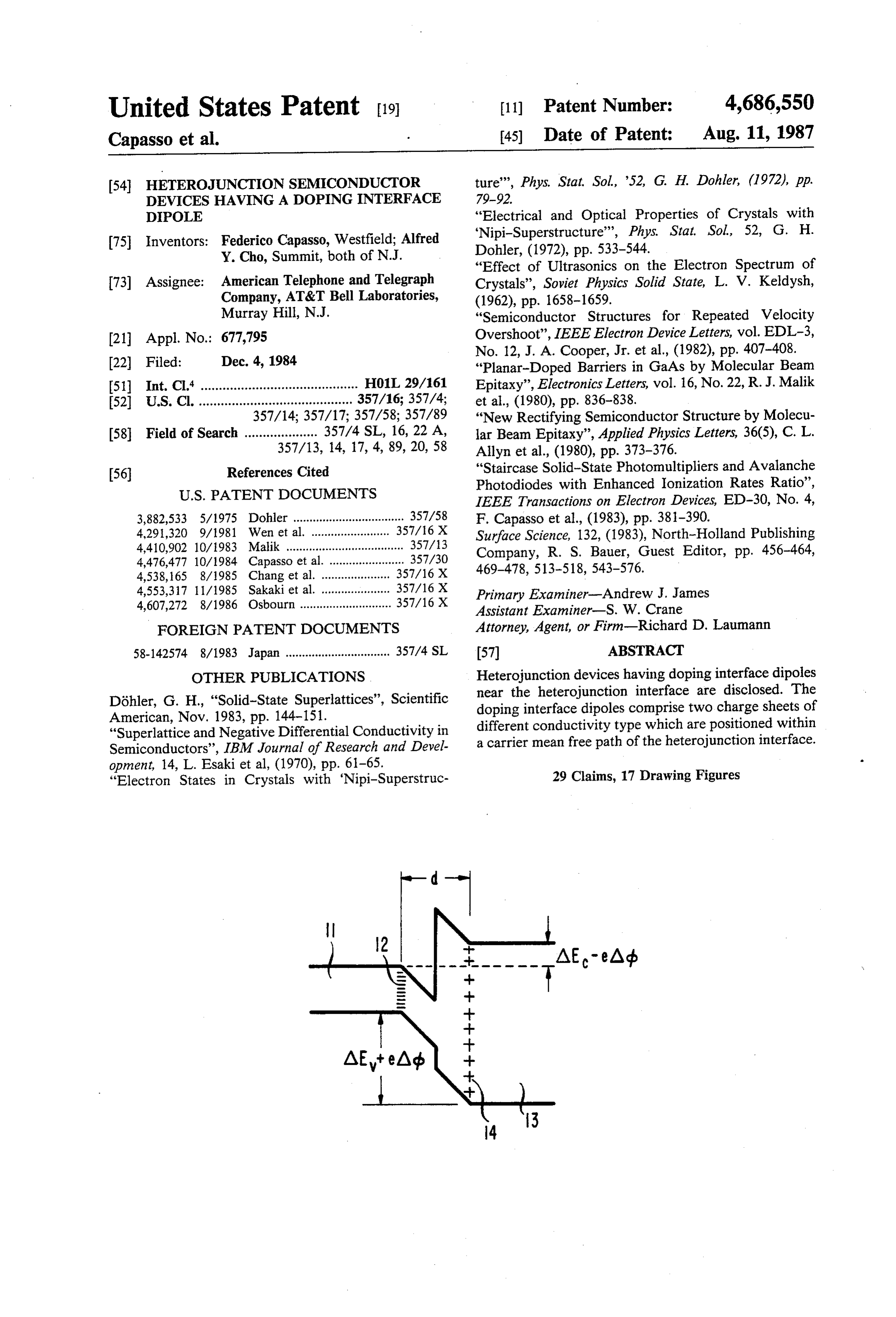
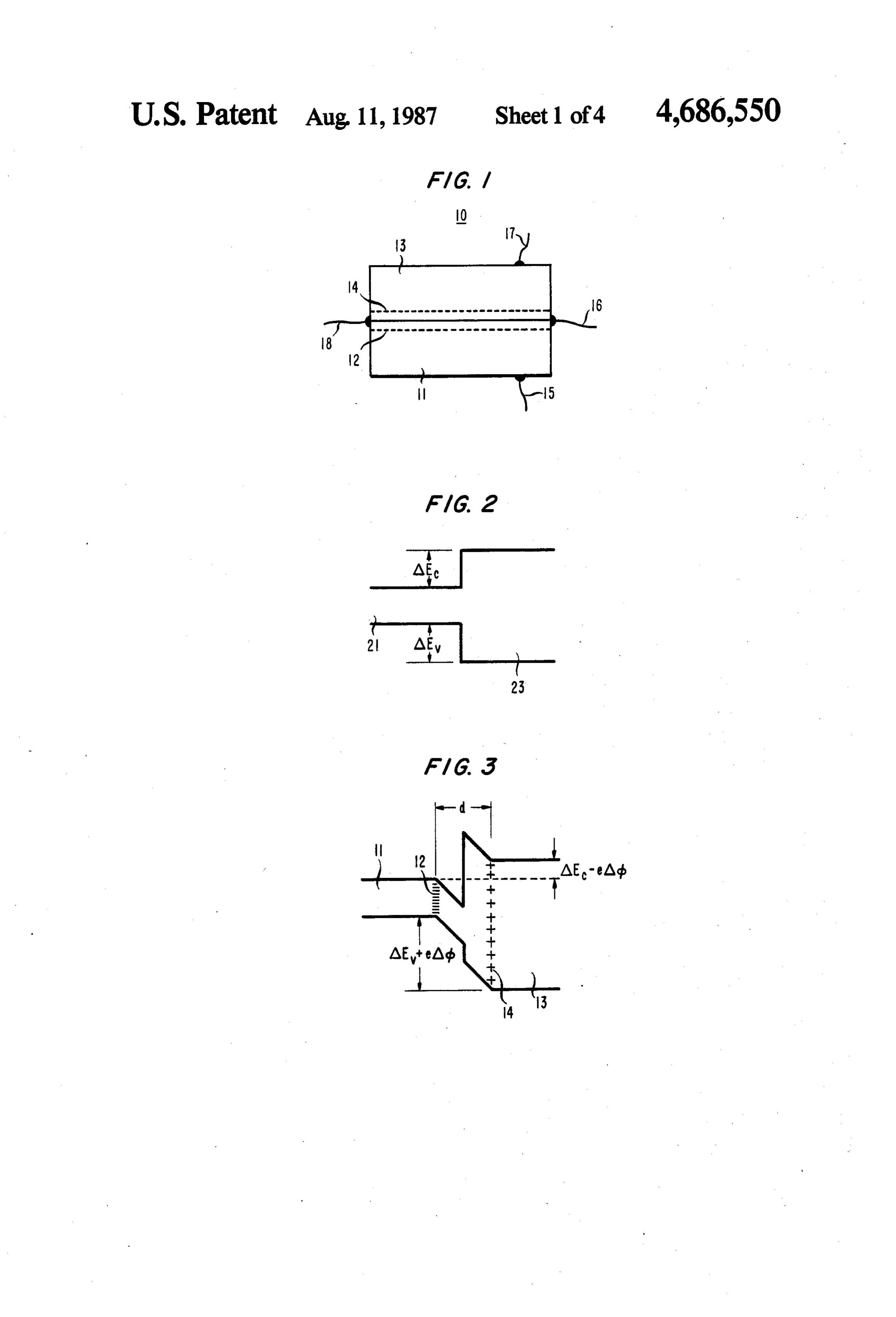
second regions having an interface; and a first charge FIG. 1 is a sectional view of a device according to sheet with a first conductivity type and a second charge sheet of a second conductivity type near the heterojunc device,this invention having a doping interface dipole. The tion interface. At least one of the charge sheets is bandgapindicated generally as 10, comprises a narrow region 11 comprising a first semiconductor and formed by heavy doping. In a preferred embodiment, 15 a wide bandgap both charge sheets are formed by doping and form a ductor. There isregion 13 comprising a second semicon doping interface dipole. In a further preferred embodi heterojunction interface.doping also a
The interface dipole at the doping interface dipole ment, the charge sheets are on opposite sides of the comprises charge sheet 12 and charge sheet 14 with the interface. The positions of the charge sheets are within two charge sheets disposed on opposite sides of the approximately the lesser of a carrier mean free path or 20 interface, i.e., sheets 12 and 14 are in regions 11 and 13, a thermal de Broglie wavelength of the interface. Still respectively. Contacts 15 and 17 electrically contact closer spacing, typically less than approximately 10 regions 11 and 13, respectively, when charge transport atomic layers from the interface, permits control of the perpendicular to the interface is desired. If charge trans energy band discontinuities by making the dipole region port parallel to the interface is desired, contacts 16 and effectively transparent to carriers. Additionally, in yet 25 18, on opposite ends of the device, may be used as may another preferred embodiment, the charge densities in any other electrode configuration which applies an both charge sheets are approximately equal. Although electric field parallel to the interface. Regions 11 and 13 the conduction and valence bands in the first region are may be intrinsic, and, as will be discussed later, they shifted with respect to the conduction and valence may alternatively have either the same or opposite con bands in the second region when the doping interface 30 ductivity types. However, the doping interface dipole is dipole is introduced, the choice of the charge orienta most effective in regions with no free charge. For pur tion of the charge sheets determines the direction of the poses of explanation, the regions will first be assumed to relative shift. This permits essentially arbitrary tuning be ideally intrinsic.
of the barrier height and the energy band discontinuit The influence of the doping interface dipoles on the ies. The doping interface dipole is useful in many types 35 energy band diagram of the device of FIG. 1 will be of heterojunction devices including lasers, photodetec discussed in reference to an exemplary heterojunction tors, field effect and bipolar transistors, etc. The carrier energy band diagram. To simplify understanding of the transport may be either parallel or perpendicular to the energy band diagram, band bending effects over the heterojunction interface. short distance depicted have been neglected. The en BRIEF DESCRIPTION OF THE DRAWING 40 ergy band diagram of such an ideal heterojunction is depicted in FIG. 2. There is a region 21 of a first semi
FIG. 1 is a sectional view of a heterojunction device conductor material and a region 23 of a second semicon having a doping interface dipole; ductor material. The first and second materials have FIG. 2 is a schematic representation of an intrinsic first and second energy bandgaps, respectively, with the semiconductor heterojunction energy band diagram; 45 first bandgap being less than the second bandgap. The FIG. 3 is the energy band diagram for the heterojunc conduction band discontinuity is AEc and the valence tion of FIG. 2 with a dipole according to our invention; band discontinuity is AEy.
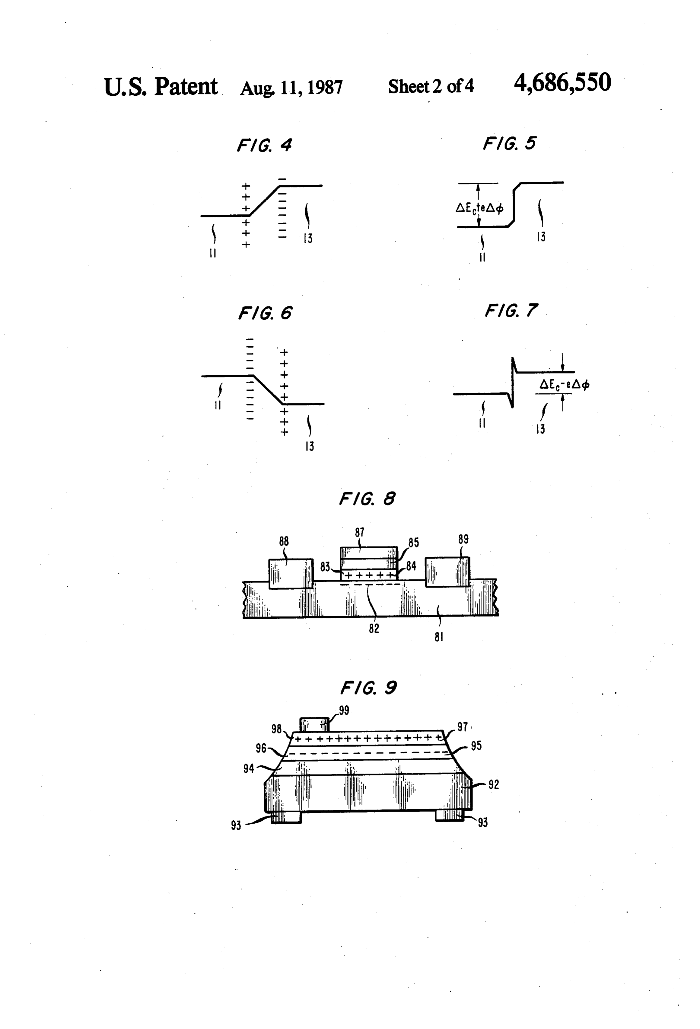
FIGS. 4–7 show the effects of the doping interface The energy band diagram for the heterojunction of dipoles on the conduction band discontinuity and the FIG. 2 and device of FIG. 1 is depicted in FIG. 3 with electrostatic potential for two dipole charge orienta the doping interface dipole being present. The positive tions; and negative charge sheets comprise ionized donors and FIG. 8 is a schematic representation of a field effect acceptors, respectively, introduced during crystal transistor according to our invention; growth. Each charge sheet has a width t and the spatial FIG. 9 is a schematic representation of an avalanche separation between the sheets is d. The width, t, is small photodetector having a doping interface dipole; 55 and, as a result, the donors and acceptors are ionized FIG. 10 is the energy band diagram for the device leading to carrier depletion in both charge sheets. The depicted in FIG. 9; width t may be taken as the width of the charge sheets FIG. 11 is a schematic representation of a heterojunc with the understanding that the elements are not to tion laser having a plurality of doping interface dipoles; scale. The charge per unit area in each sheet is ot. The FIG. 12 is the energy band diagram for the laser 60 doping interface dipole is thus essentially a microscopic depicted in FIG. 11; capacitor. The electric field between the charge sheets FIG. 13 is a schematic. representation of a bipolar is ove where e is the dielectric constant, and for simplic heterojunction transistor having a doping interface di ity of discussion, it is assumed that the dielectric con pole; stants of the two semiconductor materials are the same. FIG. 14 is the energy band diagram for the transistor 65 The potential difference, Adb, between the charge sheets depicted in FIG. 13; is Adb = ord/e. Accordingly, the doping interface dipole FIG. 15 is the conduction band diagram for a stag produces a rapid step-like potential variation near the gered heterojunction; interface, thereby changing the energy band alignment
Page 8
approximately 107/cm3. The width of the sheet is small near the interface. The relative positions of the valence enough, typically approximately 100 Angstroms, so that and conduction band in the two regions outside of the dipole region are changed. In the embodiment depicted, both the acceptor and donor charge sheets are depleted negative and positive charges are on the left and right of of carriers.
the interface, respectively. That is, sheets 12 and 14 5 As can be seen from FIGS. 3-7, there is a triangular have p- and n-type conductivity, respectively, and are energy well at the low bandgap side of the heterojunc completely depleted. The energy bands for region 11 tion interface for the accelerating dipole. However, in are both moved upward with respect to the energy practice this energy well does not behave as does a bands for region 13. Outside of the dipole region, the classical energy well, but rather as a quantum well. This conduction band offset is reduced by eadb where e is the 10. is understood when it is realized that the electric field in electronic charge while the valence band offset is in the dipole region is typically about 105 V/cm, and the creased by the same amount. dipole potential difference is approximately 0.1 to 0.2 This change in the energy band diagram is better eV. The skilled artisan can now easily show that the understood from the following considerations. The first, i.e., lowest energy level in the well, is very close to potential difference due to the dipole is ord/e. Accord 15 the top of the well. If the carriers are ballistic, they will, ingly, the valence band barrier may be viewed as having increased by the dipole potential energy eord/e. Similar inscattereffect, not see the energy well because they do not in it. That is, the well width is less than the considerations apply to the conduction band barrier. carrier mean free path. If the carriers do thermalize, The effect of the doping interface dipole on the en their energy states will be near the top of the quantum ergy band diagram may perhaps be better understood 20 by reference to FIGS. 4-7. These energy band diagrams well because of the quantum effects. This effectively will be discussed with respect to electrons moving from decreases the height of the barrier and greatly increases the probability of thermionic emission of electrons over left to right. FIGS. 4-5 depict the potential variation the and shift in conduction band discontinuity, respectively, sionbarrier. An analysis shows that the thermionic emis probability increases approximately by exp for a retarding doping interface doping and FIGS. 6-7 25 (eAdb/2kT). As kT is small, approximately 0.025 eV, at are the corresponding diagrams for an accelerating doping interface dipole. The retarding dipole has posi room temperature, this is a considerable enhancement in tive and negative charge sheets in the narrow and wide the emission probability even if eAdb is only 0.1 eV. It is bandgap regions, respectively. The accelerating dipole also apparent that electroms can easily tunnel through has negative and positive charge sheets in the narrow 30 the triangular barrier provided that it is thin i.e., less and wide bandgap regions, respectively. than approximately 100 Angstroms in width. As can be seen from FIG. 4, the potential increases The energy band discontinuities may be varied if the across the dipole and the conduction band discontinuity charge sheets forming the doping interface dipole are increases, FIG. 5, thus retarding the electron. The po within several, typically 1 to 5, atomic layers of the tential decreases as shown in FIG. 6 resulting in the 35 interface. If the dipole potential difference, Adb, is decrease in conduction band discontinuity shown in dropped over several atomic layers, the valence band FIG. 7. Accordingly, the electron will be accelerated. discontinuity in FIG. 3 is effectively increased by eadb Similar considerations apply, as will be readily appreci where Adb is the dipole potential. The dipole potential ated by those skilled in the art, to the valence band reduces the energy difference between the conduction discontinuity and the effect of the dipole on hole trans 40 band edges thus reducing the conduction band disconti port properties. nuity to AEc-eAdb. A similar analysis is now easily The charge sheets should be within the lesser of ap made by the skilled artisan for the other dipole orienta proximately an electron thermal de Broglie wavelength tion.
or an electron mean free path of the interface for barrier Devices using doping interface dipoles near a hetero height tuning. In the embodiment depicted, the tuning 45 junction interface are conveniently fabricated by has been done primarily to enhance the electron trans growth techniques, such as molecular beam epitaxy or port characteristics. If the tuning is performed primarily metallorganic chemical vapor deposition, that permit for holes, the distance of the charge sheets from the fabrication of abrupt compositional and doping profiles. heterojunction will be determined by the hole thermal The semiconductor materials are selected from the de Brogile wavelength or mean free path. They typi group consisting of Group III-V, Group IV and Group cally will be within 500 Angstroms of the interface. The 50 II-VI semiconductors. Particularly useful combinations thermal de Broglie wavelength is determined by using include InGaAsP/InP, AlGaAsSb/GaSb, AlGaAsSb the de Broglie equation, A=h/p, where A is the wave /AlSb, and AlInGaAs/AlInAs.
length, his Planck's constant and p is the momentump Other embodiments in addition to those explicitly is mvith where m is the carrier effective mass and vih is 55 mentioned previously with respect to FIG. 3 are con the thermal velocity, templated. For example, regions 11 and 13 may both have n-type conductivity or p-type conductivity, re spectivity, or they may have different, i.e., first and with F second, conductivity types. As will be readily appreci 60 ated by those skilled in the art, the energy band diagram where T is the absolute temperature and k is Bolt at the interface will not be the same as that depicted in FIG. 3 for other conductivity configurations. Other zmann's constant. Greater distances are undesirable because of the full possible effect of the doping interface to modifications of the embodiment depicted with respect dipole on carrier transport properties may not be real ductivity FIGS. 1-3 are contemplated. For example, the con ized. The doping density is typically within the range versed. The 65 types of the two charge sheets may be re from approximately 107/cm3 to approximately discussion of FIGS. 4 and 5 shows the 1019/cm3. That is, the charge sheet is heavily doped skilled artisan that the changes in the valence and con means that it has a doping concentration, of at least duction band discontinuities will also be reversed, with
Page 9
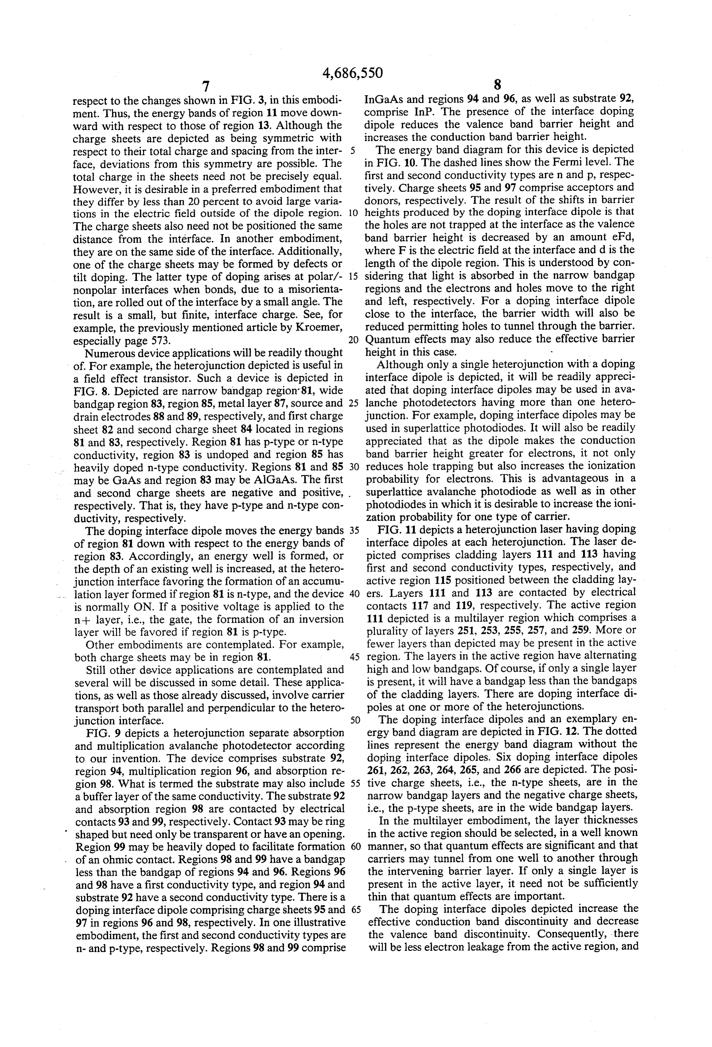
respect to the changes shown in FIG. 3, in this embodi InGaAs and regions 94 and 96, as well as substrate 92, ment. Thus, the energy bands of region 11 move down comprise InP. The presence of the interface doping ward with respect to those of region 13. Although the dipole reduces the valence band barrier height and charge sheets are depicted as being symmetric with increases the conduction band barrier height. respect to their total charge and spacing from the inter The energy band diagram for this device is depicted face, deviations from this symmetry are possible. The in FIG. 10. The dashed lines show the Fermi level. The total charge in the sheets need not be precisely equal. first and second conductivity types are n and p, respec However, it is desirable in a preferred embodiment that tively. Charge sheets 95 and 97 comprise acceptors and they differ by less than 20 percent to avoid large varia donors, respectively. The result of the shifts in barrier tions in the electric field outside of the dipole region. 10 heights produced by the doping interface dipole is that The charge sheets also need not be positioned the same the holes are not trapped at the interface as the valence distance from the interface. In another embodiment, band barrier height is decreased by an amount eFd, they are on the same side of the interface. Additionally, where F is the electric field at the interface and d is the one of the charge sheets may be formed by defects or length of the dipole region. This is understood by con tilt doping. The latter type of doping arises at polar/- 15 sidering that light is absorbed in the narrow bandgap nonpolar interfaces when bonds, due to a misorienta regions and the electrons and holes move to the right tion, are rolled out of the interface by a small angle. The and left, respectively. For a doping interface dipole result is a small, but finite, interface charge. See, for close to the interface, the barrier width will also be example, the previously mentioned article by Kroemer, reduced permitting holes to tunnel through the barrier. especially page 573. 20 Quantum effects may also reduce the effective barrier Numerous device applications will be readily thought height in this case.
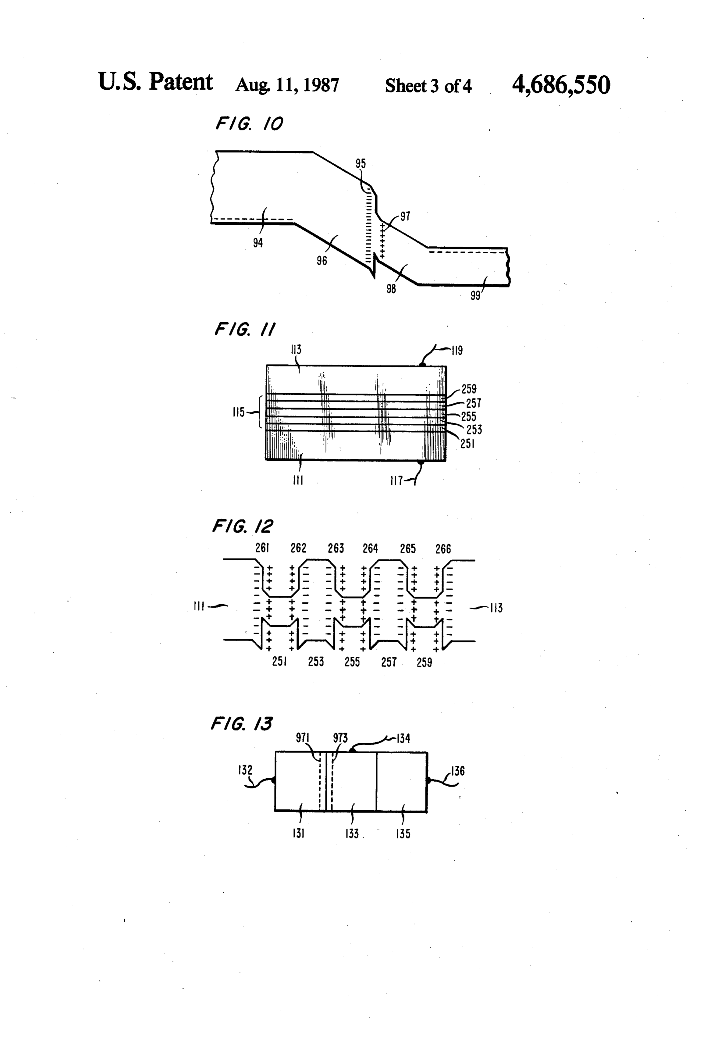
of For example, the heterojunction depicted is useful in Although only a single heterojunction with a doping a field effect transistor. Such a device is depicted in interface dipole is depicted, it will be readily appreci FIG. 8. Depicted are narrow bandgap region'81, wide ated that doping interface dipoles may be used in ava bandgap region 83, region 85, metal layer 87, source and 25 lanche photodetectors having more than one hetero drain electrodes 88 and 89, respectively, and first charge junction. For example, doping interface dipoles may be sheet 82 and second charge sheet 84 located in regions used in superlattice photodiodes. It will also be readily 81 and 83, respectively. Region 81 has p-type or n-type appreciated that as the dipole makes the conduction conductivity, region 83 is undoped and region 85 has band barrier height greater for electrons, it not only heavily doped n-type conductivity. Regions 81 and 85 30 reduces hole trapping but also increases the ionization may be GaAs and region 83 may be AlGaAs. The first probability for electrons. This is advantageous in a and second charge sheets are negative and positive, superlattice avalanche photodiode as well as in other respectively. That is, they have p-type and n-type con photodiodes in which it is desirable to increase the ioni ductivity, respectively. zation probability for one type of carrier. The doping interface dipole moves the energy bands 35 FIG. 11 depicts a heterojunction laser having doping of region 81 down with respect to the energy bands of interface dipoles at each heterojunction. The laser de region 83. Accordingly, an energy well is formed, or picted comprises cladding layers 111 and 113 having the depth of an existing well is increased, at the hetero first and second conductivity types, respectively, and junction interface favoring the formation of an accumu active region 115 positioned between the cladding lay lation layer formed if region 81 is n-type, and the device 40 ers. Layers 111 and 113 are contacted by electrical is normally ON. If a positive voltage is applied to the contacts 117 and 119, respectively. The active region n-- layer, i.e., the gate, the formation of an inversion 111 depicted is a multilayer region which comprises a layer will be favored if region 81 is p-type. plurality of layers 251, 253, 255, 257, and 259. More or Other embodiments are contemplated. For example, fewer layers than depicted may be present in the active both charge sheets may be in region 81. 45 region. The layers in the active region have alternating Still other device applications are contemplated and high and low bandgaps. Of course, if only a single layer several will be discussed in some detail. These applica is present, it will have a bandgap less than the bandgaps tions, as well as those already discussed, involve carrier of the cladding layers. There are doping interface di transport both parallel and perpendicular to the hetero poles at one or more of the heterojunctions. junction interface. 50 The doping interface dipoles and an exemplary en FIG. 9 depicts a heterojunction separate absorption ergy band diagram are depicted in FIG. 12. The dotted and multiplication avalanche photodetector according lines represent the energy band diagram without the to our invention. The device comprises substrate 92, doping interface dipoles. Six doping interface dipoles region 94, multiplication region 96, and absorption re 261, 262, 263,264, 265, and 266 are depicted. The posi gion 98. What is termed the substrate may also include 55 tive charge sheets, i.e., the n-type sheets, are in the a buffer layer of the same conductivity. The substrate 92 narrow bandgap layers and the negative charge sheets, and absorption region 98 are contacted by electrical i.e., the p-type sheets, are in the wide bandgap layers. contacts 93 and 99, respectively. Contact 93 may be ring In the multilayer embodiment, the layer thicknesses shaped but need only be transparent or have an opening. in the active region should be selected, in a well known Region 99 may be heavily doped to facilitate formation 60 manner, so that quantum effects are significant and that - of an ohmic contact. Regions 98 and 99 have a bandgap carriers may tunnel from one well to another through less than the bandgap of regions 94 and 96. Regions 96 the intervening barrier layer. If only a single layer is and 98 have a first conductivity type, and region 94 and present in the active layer, it need not be sufficiently substrate 92 have a second conductivity type. There is a thin that quantum effects are important. doping interface dipole comprising charge sheets 95 and 65 The doping interface dipoles depicted increase the 97 in regions 96 and 98, respectively. In one illustrative effective conduction band discontinuity and decrease embodiment, the first and second conductivity types are the valence band discontinuity. Consequently, there n- and p-type, respectively. Regions 98 and 99 comprise will be less electron leakage from the active region, and
Page 10
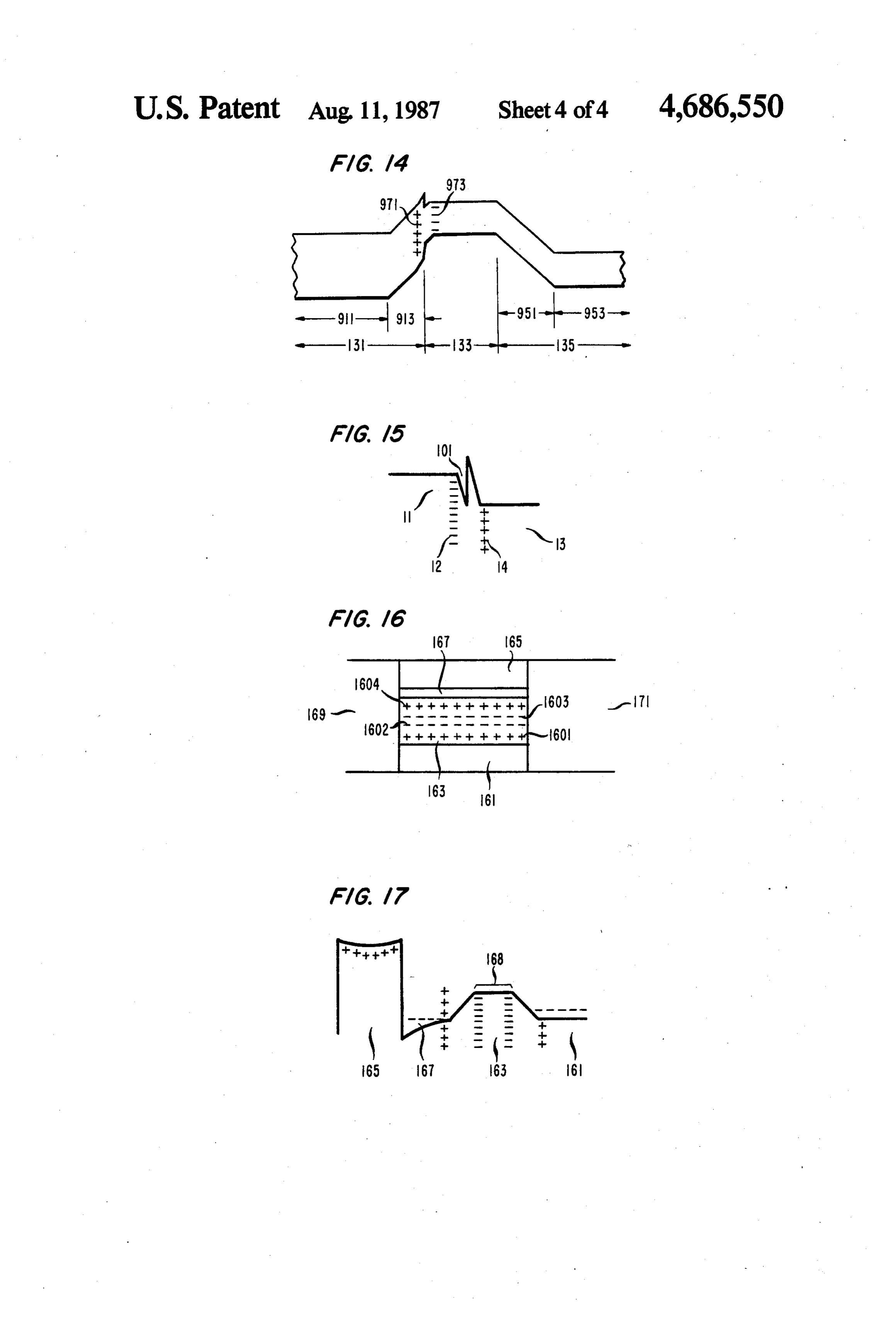
To is improved. A higher value of To means that lasing bandgap region 161, regionhighly device depicted comprises doped n-type narrow will begin at a lower threshold current, Jih, and Jih is wide bandgap region 165. Region 165is isundoped, 163 which doped and and proportional to exp(T/T) where T is the temperature of the heat sink that the laser is mounted on. The holes, consequently, a two-dimensional electron gas 167 forms in most semiconductors, have a high effective mass and four at the interface of regions 163 and 165. Region 163 has will not readily pass over or through the reduced bar with charge sheets forming two doping interface dipoles alternate charge configurations. The dipoles cause rier. The doping interface dipoles need not be present at all heterojunction interfaces. It will also be readily ap the conduction band to move upward and result in the preciated that other layers, for example, buffer layers, formation 169 and of two potential wells. Electrical contacts 171 are formed by highly doped n-- regions may be present. O
FIG. 13 depicts a bipolar heterojunction transistor contacting opposite sides of the regions described. The energy band diagram of this device is depicted in having an interface doping dipole. Depicted are emitter FIG. 17. As the electric field between contacts 169 and region 131, base region 133 and collector region 135.
The emitter and collector regions have a first conduc acquireincreased, 171 is some electrons in the electron gas 167 tivity type and the base region has a second conductiv 15 rier 168enough energy to surmount the potential bar and move to the degenerately doped region ity type. The emitter, base and collector regions are 161. In this region, they have lower mobility than they contacted by electrical contacts 132, 134 and 136, re had in gas 167 and negative differential resistance re spectively. In a preferred embodiment, the emitter re sults.
gion has a bandgap greater than that of the base region.
The interface of the emitter and base regions has a dop 20 skilled Still other embodiments will be thought of by those ing interface dipole comprising charge sheets 971 and in the art. For example, although FIG. 2 is de 973 which are donor and acceptor, respectively. The scribed conductors, with respect to wide and narrow bandgap semi there are also embodiments in which the doping interface dipole increases emitter injection effi ciency, and current gain gas the valence band barrier is 25 althoughconduction band of region 21 is below that of region 23 increased at the emitter-base interface. region 21 has a bandgap greater than that of The device operation may be better understood by region region 23. In this case, electrons will be confined in reference to the energy band diagram, depicted in FIG. 21 and holes will be confined in region 23. Still 14, for the device of FIG. 13. The emitter region has a other variations will be ready thought of. What is claimed is:
lightly doped n-type region 913 adjacent the base region and an n-- region 911 further away. The base region has 30 1. A heterojunction device comprising at least a first p-- conductivity and the collector region has n-type region of a first semiconductor material and at least a conductivity with a lightly doped region 951 adjacent second region of a second semiconductor material, said the base region, and a more heavily doped region 953 first and said second regions having a first heterojunc adjacent region 951. It may be desirable to have an comprising tion interface, and a first interface dipole, said dipole
undoped region near the emitter-base interface on the sheet, said first a first charge sheet and a second charge base side to avoid dopant diffusion from the base into separated fromand each second charge sheets being spatially other and comprising ionized do the emitter. The negative charge sheet is desirably placed within this undoped region. The doping inter nors and acceptors, respectively, at least one of said charge sheets being a heavily doped region, said charge face dipole increases the effective valence band discon 40 sheets being within the lesser of a carrier mean free path tinuity thereby increasing hole confinement in the base or a thermal de Broglie wavelength of said interface. region. This results in increased current gain. It should 2. A device as recited in claim 1 in which said charge be noted that the emitter could be doped uniformly n-type. Only the acceptor sheet in the base is then re sheets are in the same region.
quired to form the desired doping interface dipole. 3. A device as recited in claim 1 in which said charge It is evident that a tunneling emitter is also possible if 45 sheets are in different regions. the conduction band of the base region is below the charge 4. A device as recited in claim 2 or 3 in which said bottom of the potential well in the emitter region, i.e., if sheets are less than the thermal de Broglie wave the energy bands outside the dipole region are stag length from said interface. 5. A device as recited in claim 4 in which said charge gered.
The conduction band diagram, FIG. 15, for a hetero 50 sheets are less than approximately 10 atomic layers from junction such as that depicted in FIG. 3, with the dop said6. interface.
ing interface dipole having a potential such that the regionA has device as recited in claim 1 in which said first a bandgap greater than the bandgap of said conduction band of the wide bandgap region 13 is second region.
below the conduction band of the narrow bandgap 55 7. A device as recited in claim 6 comprising a two-di region 11, is depicted. Electrons can be trapped in the triangular energy well. The electrons in the well are in mensional carrier gas at said interface.
a metastable energy state, i.e., they are stored, which second 8. A device as recited in claim 7 comprising first and they can leave by a tunneling process. The tunneling electrical contacts to said second region and a process may, however, have a relatively long lifetime. third electrical contact to said first region. Still other device applications will be readily thought 60 9. A device as recited in claim 6 further comprising a of. For example, real space transfer devices are contem third third region of a third semiconductor material, said region and said second region having a second plated. If an electric field is now applied parallel to the interface, the dipole will reduce the threshold field interface.
required for negative differential resistance due to real and10.said A device as recited in claim 9 in which said first second regions have opposite conductivity space transfer from the well the electron is in initially to 65 a second well. A useful structure for such a device is types.
depicted in FIG. 16 and the corresponding energy band region 11. A device as recited in claim 10 in which said third diagram is depicted in FIG. 17. The real space transfer has the conductivity type of said first region.
Page 11
12. A device as recited in claim 11 further comprising 20. A device as recited in claim 19 in which said first first, second and third electrical contacts to said first, and third regions have opposite conductivity types. second and third regions, respectively. 21. A device as recited in claim 1 further comprising 13. A device as recited in claim 6 in which said first means for establishing an electric field parallel to said interface.
and said second regions have the same conductivity 22. A device as recited in claim 1 further comprising type. means for establishing an electric field perpendicular to 14. A device as recited in claim 13 further comprising said interface.
a third region, said third region and said first region 23. A device as recited in claim 1 in which said charge having a second interface. O sheets have thicknesses less than approximately 100 15. A device as recited in claim 14 in which said third Angstroms.
region has a bandgap greater than the bandgap of said 24. A device as recited in claim 1 in which said charge second region. sheets having doping concentrations within the range 16. A device as recited in claim 15 in which said third from approximately 1017/cm3 to approximately region has a conductivity type opposite to said conduc 15 1019/cm3.
25. A device as recited in claim 1 in which said semi tivity type of said region. conductor materials are selected from the group con 17. A device as recited in claim 16 further comprising sisting of Group IV, Group III-V and Group II-VI first and second electrical contacts to said second and semiconductors.
third regions, respectively. 20 26. A device as recited in claim 25 in which at least 18. A device as recited in claim 9 in which said third one of said semiconductor materials comprises a Group region has a bandgap greater than the bandgap of said IV element.
second region. 27. A device as recited in claim 25 in which at least one of said semiconductor materials comprises a Group 19. A device as recited in claim 18 further comprising 25 III-V a second doping interface dipole, said second dipole compound semiconductor.
28. A device as recited in claim 27 in which said comprising a third charge sheet and a fourth charge Group III-V semiconductors are selected from the sheet, said third and fourth charge sheets being spatially group consisting of InCaAsP, AlGaAsSb, and AlIn separated from each other and comprising ionized do GaAs.
nors and acceptors, respectively, at least one of said 30 29. A device as recited in claim 6 in which the con charge sheets being a heavily doped region, being duction band of said first region is below the conduction within the lesser of a carrier mean free path or a thermal band of said second skregion.
de Broglie wavelength of said second interface.
Provenance
- Collection
- Cited prior art
- Original PDF
- patentimages.storage.googleapis.com →
- Filed
- 1984-12-04
- Pages
- 11
- Method
- pdftotext (the PDF's own text layer) + pdftoppm 300dpi page scans
- Source
- Google Patents bibliographic record
- Granted
- 1987-08-11
- Inventors
- Federico Capasso; Alfred Y. Cho; AT&T Bell Laboratories Inc
- Transcribed from
- patentimages.storage.googleapis.com →