patent · US4716445
Heterojunction bipolar transistor having a base region of germanium
29 December 1987
Page 1 — bibliographic record
United States Patent (19) 11 Patent Number: 4,716,445 Sone 45) Date of Patent: Dec. 29, 1987 54. HETEROJUNCTION BIPOLAR FOREIGN PATENT DOCUMENTS
TRANSISTOR HAVING A BASE REGION OF
GERMANUM 0159273 10/1985 European Pat. Off........... 357/4 SL 75 Inventor: Jun'ichi Sone, Tokyo, Japan OTHER PUBLICATIONS 73) Assignee: NEC Corporation, Tokyo, Japan H. Kroemer, “Heterostructure Bipolar Transistors and Integrated Circuits', Proceedings of the IEEE, vol. 70, 21 Appl. No.: 4,931 No. 1, Jan. 1982, pp. 13-25. "OYO BUTURI”, Japanese Society of Applied Phys 22 Filed: Jan. 20, 1987 ics, vol. 54, No. 11, pp. 1192-1197, 7/15/85. (30) Foreign Application Priority Data Primary Examiner-Martin H. Edlow Assistant Examiner-D. Featherstone
Jan. 17, 1986 JPl Japan .................................... 61-8587 Attorney, Agent, or Firm-Sughrue, Mion, Zinn, Macpeak & Seas
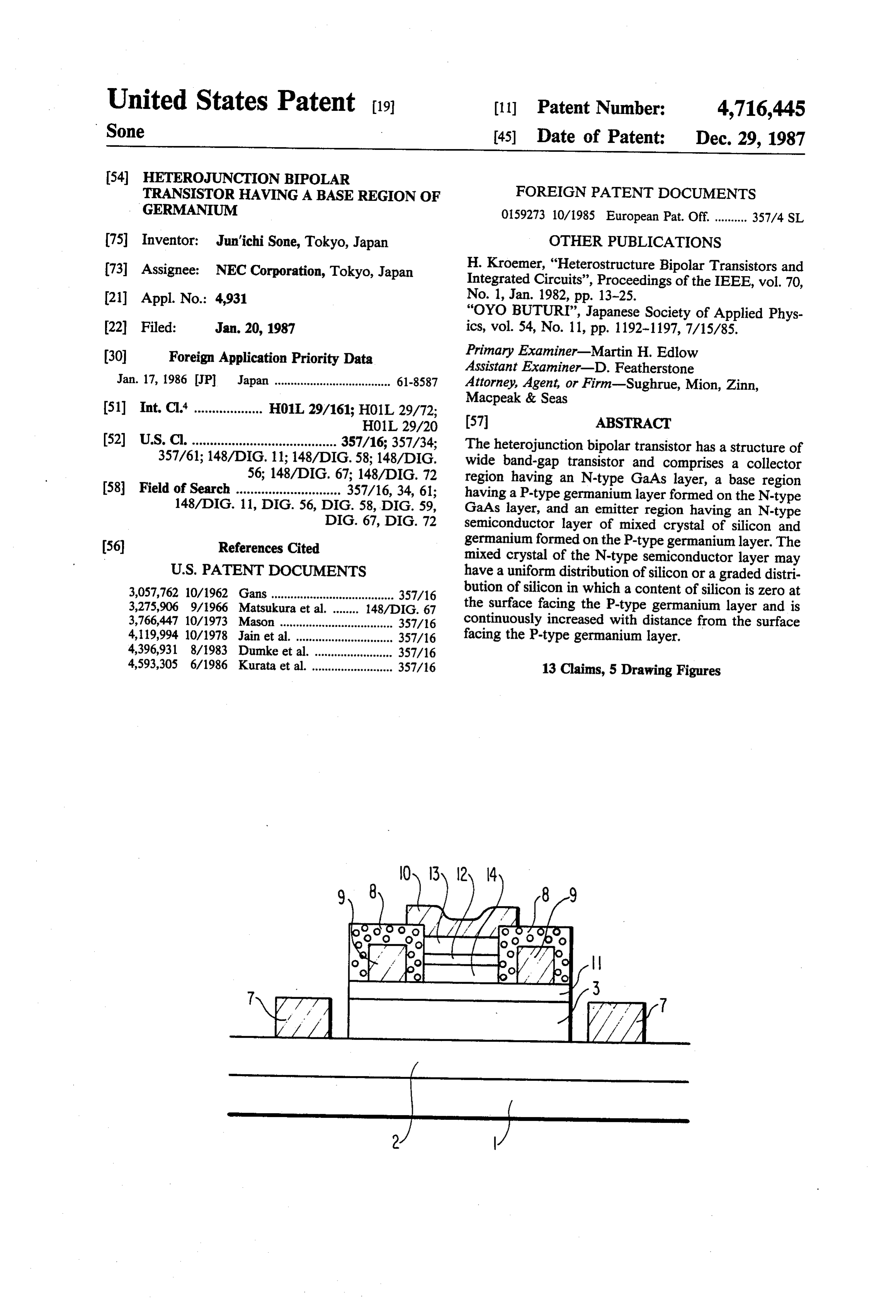
52 U.S. C. ........................................ 357/16; 357/34; The heterojunction bipolar transistor has a structure of 357/61; 148/DIG. 11; 148/DIG.58; 148/DIG. wide band-gap transistor and comprises a collector 56; 148/DIG. 67; 148/DIG. 72 region having an N-type GaAs layer, a base region 58 Field of Search ............................. 357/16, 34, 61; having a P-type germanium layer formed on the N-type 148/DIG. 11, DIG. 56, DIG. 58, DIG. 59, GaAs layer, and an emitter region having an N-type DIG. 67, DIG. 72 semiconductor layer of mixed crystal of silicon and (56) References Cited germanium formed on the P-type germanium layer. The mixed crystal of the N-type semiconductor layer may
3,057,762 10/1962 Gans...................................... 357/16 bution of silicon in which a content of silicon is zero at 3,275,906 9/1966 Matsukura et al. ........ 148/TDIG. 67 the surface facing the P-type germanium layer and is 3,766,447 10/1973 Mason ................................... 357/16 continuously increased with distance from the surface 4, 19,994 10/1978 Jain et al. ...... ... 357/16 facing the P-type germanium layer. 4,396,931 8/1983 Dumke et al. .... ... 357/16 4,593,305 6/1986 Kurata et al. ......................... 357/16 13 Claims, 5 Drawing Figures
Page 2
Drawing sheet — no readable text.
Page 3
Drawing sheet — no readable text.
Page 4
HETEROJUNCTON BIPOLAR TRANSISTOR tor region, Ge as a base region and GaAs as an emitter HAVING A BASE REGION OF GERMANIUM region. Ge used as the base region has a low energy band-gap of 0.66 eV and a hole mobility of 4 or 5 times
of GaAs or Si and is an indirect transition type semicon ductor. Therefore, a low voltage drive, a low power 1. Field of the Invention consumption, a low base resistance and an improved The present invention relates to a heterojunction injection efficiency of carrier are achieved. bipolar transistor, and more particularly to a wide band However, as pointed out in "Proceedings of the gap bipolar transistor having a base region of germa IEEE' Vol. 70, No. 1, page 23, fifth paragraph of left
2. Description of the Related Art Including Informa out side column, it is very hard to grow GaAs on Ge with interface defects. This GaAs-Ge-GaAs structure is tion Disclosed Under SS 1.97-199: not a practical resolution for the above-mentioned The so-called wide band-gap bipolar transistor has been reported in "Proceedings of the IEEE' Vol. 70, drawbacks. Moreover, the GaAs as the emitter region No. 1 (January 1982) pages 13 to 23, the article "Hete ohmic contactthewith 15 still remains difficulty for obtaining a low-resistive a metallic emitter electrode.
rostructure Bipolar Transistors and Integrated Cir cuits' by Herbert Kroemer. It is a heterojunction tran SUMMARY OF THE INVENTION sistor having an emitter made of a semiconductor hav ing an energy band-gap wider than the base. The injec tionIt is, therefore a primary object of the present inven to provide a bipolar transistor having a realizable tion efficiency of minority carrier from emitter to base 20 is improved to obtain an increased current gain. structure and operable in high speed with a low voltage An example of the wide band-gap bipolar transistorin signal without consuming a large power. the prior art has been proposed in “OYO BUTURI” It is another object of the present invention to pro published by the Japanese Society of Applied Physics, vide a heterojunction bipolar transistor having a base Vol. 54, No. 11 pages 1192 to 1197 and has a collector 25 region of germanium and a whole structure realizable composed of an N-GaAs deposited on an insulating with present manufacturing technology.
GaAs substrate and an N-GaAs formed on the N According to the present invention, there is provided GaAs, a base composed of P-GaAs and an emitter a heterojunction bipolar transistor including a collector composed of an N-AlGaAs formed on the P-GaAs and region having a GaAs layer of one conductivity type, a an N-GaAs formed on the N-AlGaAs. AlGaAs has an 30 base region having a germanium layer of the other con energy band-gap of about 1.9 eV which is wider than ductivity type formed in contact with the GaAs layer GaAs of 1.42 eV. Thus, an improved electron injection and an emitter region having a semiconductor layer of efficiency and an increased current gain is obtained. mixed crystal of silicon and germanium of the one con Electron in GaAs has a mobility of about 4,600 ductivity type formed on the germanium layer. The cm/V.sec which is greater than Si, and has a high 35 mixed crystal semiconductor layer may have a uniform saturated electron drift velocity of about 1.8x10⁷ distribution of silicon in germanium or a graded distri cm/sec. Thus, electrons run through the base and col lector regions in a very short time, resulted in a high bution of silicon. In the case of the uniform distribution, the content of silicon is between 10 mol. 9% and 40 mol.
speed operation.
On the other hand, the wide band-gap bipolar transis %. In the case of the graded distribution, the content of tor in the prior-art has many drawbacks. The energy silicon increases with distance from the interface be tween the base and emitter regions from 0 mol. 9% to a band-gap of GaAs is wider than silicon of 1.12 eV. Due value between 10 mol. 26 and 40 mol. 2. to this wide band-gap, the prior art transistor requires a The growth of germanium on GaAs and the growth high voltage signal for its electrical operation and con of the mixed crystal layer of silicon and germanium on sumes a large power, compared to a silicon transistor. 45 germanium may be performed without interface defect Moreover, GaAlAs of emitter region and N-GaAs of collector region have a difficulty in forming a low-resis by use of molecular beam epitaxy. The whole structure tive ohmic contact with a metal. In the prior-art transis can be easily constructed. Particularly, because the tor, N-GaAs is interposed between the N-GaAlAs of emitter is of the mixed crystal which has a lower energy emitter region and an emitter electrode of metal and 50 band-gap of 0.8 to 0.9 eV than GaAs of 1.42 eV, a low between the N-GaAs of collector region and a collector resistive ohmic contact with metal is easily obtained. electrode of metal for improving the ohmic contact The structure for emitter region and emitter electrode property. Therefore, the device structure is compli may be simplified.
cated and causes a difficulty in manufacturing the same. The base region is made of germanium. Therefore, Furthermore, GaAs is a semiconductor of direct transi 55 the bipolar transistor of the present invention is driven tion type, while Si and Ge are an indirect transition with a low voltage signal and consumes a small power. type. Life time of minority carrier in the direct transi The injection efficiency of minority carriers is im tion type semiconductor is shorter than in the indirect proved, due to the indirect transition in germanium. transition type semiconductor. Considerable part of This improved injection efficiency raises the current electrons injected into the P-GaAs base region disap 60 gain. Furthermore, the germanium has a large electron pear by recombination. This disappearance lowers the mobility. The energy band-gap of the mixed crystal of injection efficiency of minority carriers injected into silicon and germanium is about 0.77 eV and is larger base region. From this point of view, it is preferable to than the energy band-gap of germanium which is about use the indirect transition type semiconductor such as Si 0.66 eV. This fact shows the transistor of the present and Ce for the base region. 65 invention is a wide band-gap transistor. Due to the facts For improving some of the above-explained draw of large electron mobility and the wide band-gap tran backs, it has been proposed in "Proceedings of the sistor structure, the operation of the present invention is IEEE' Vol. 70, No. 1, page 23 to use GaAs as a collec very fast.
Page 5
BRIEF DESCRIPTION OF THE DRAWINGS N+-GaAs layer 2 is formed with a thickness of 1 um and an impurity concentration of 2X 1018 cm3. The
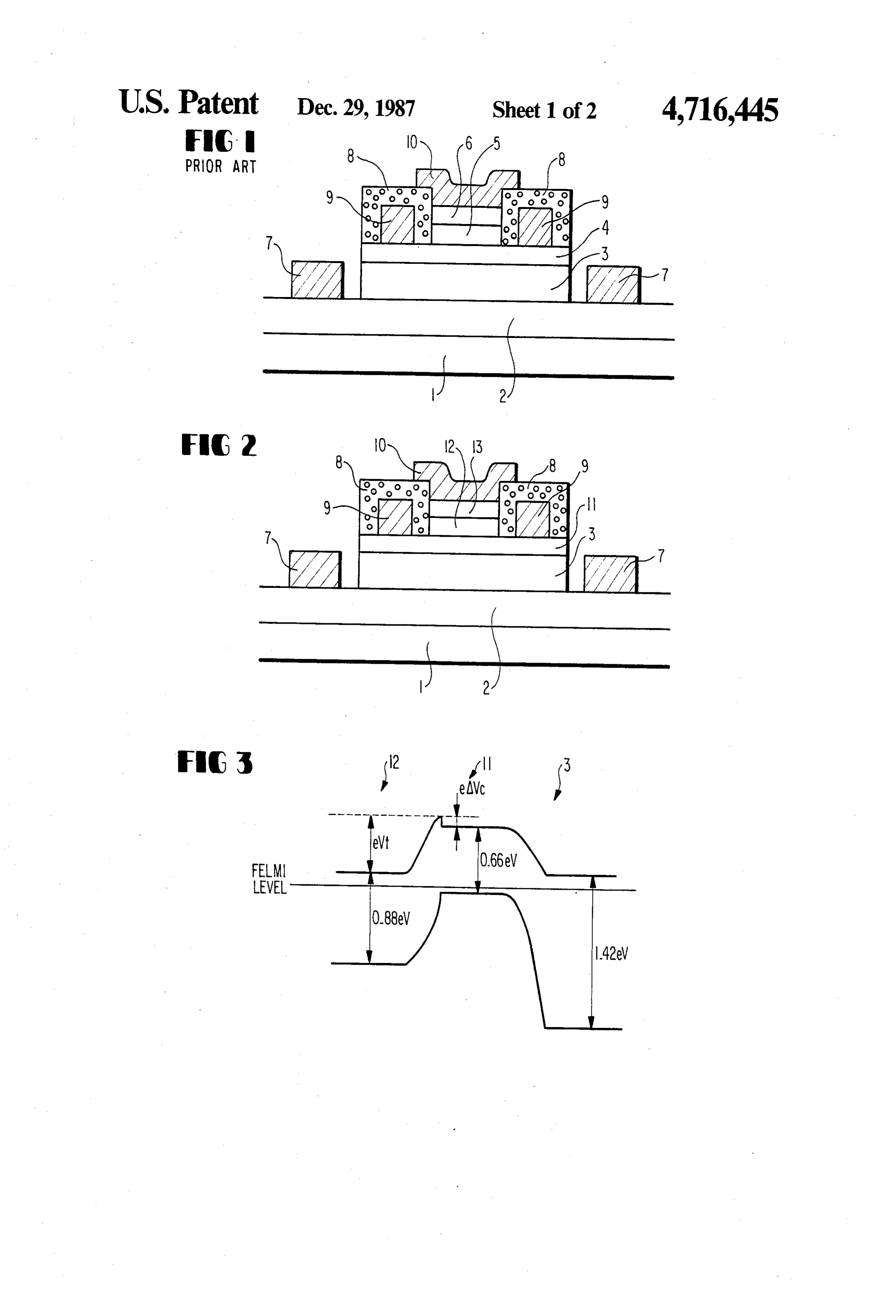
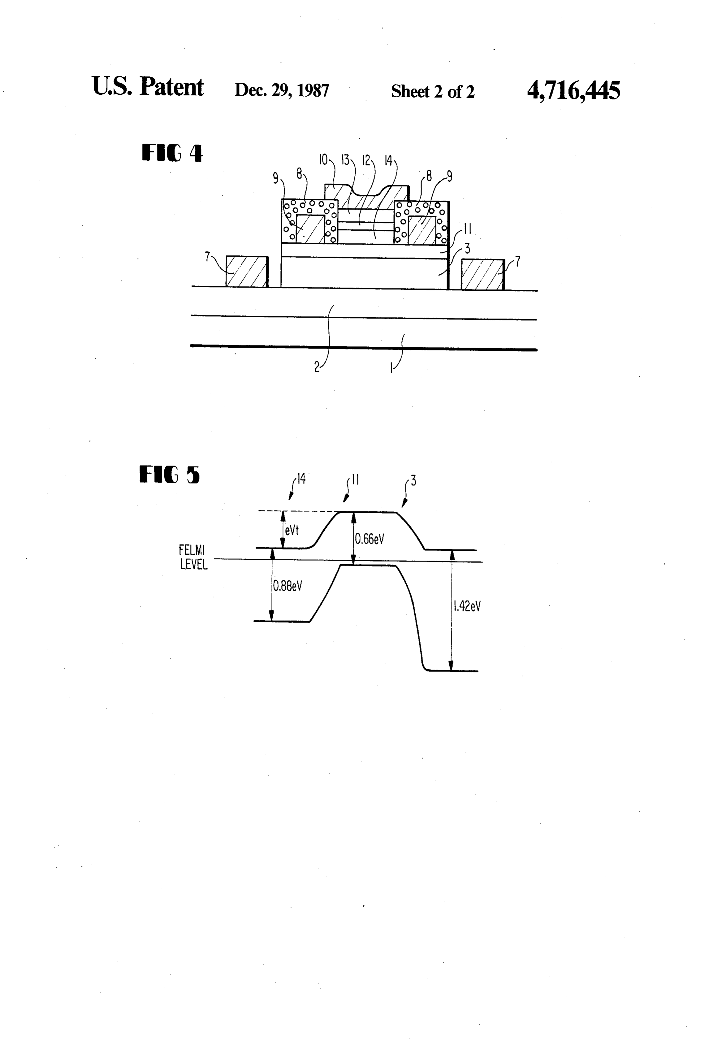
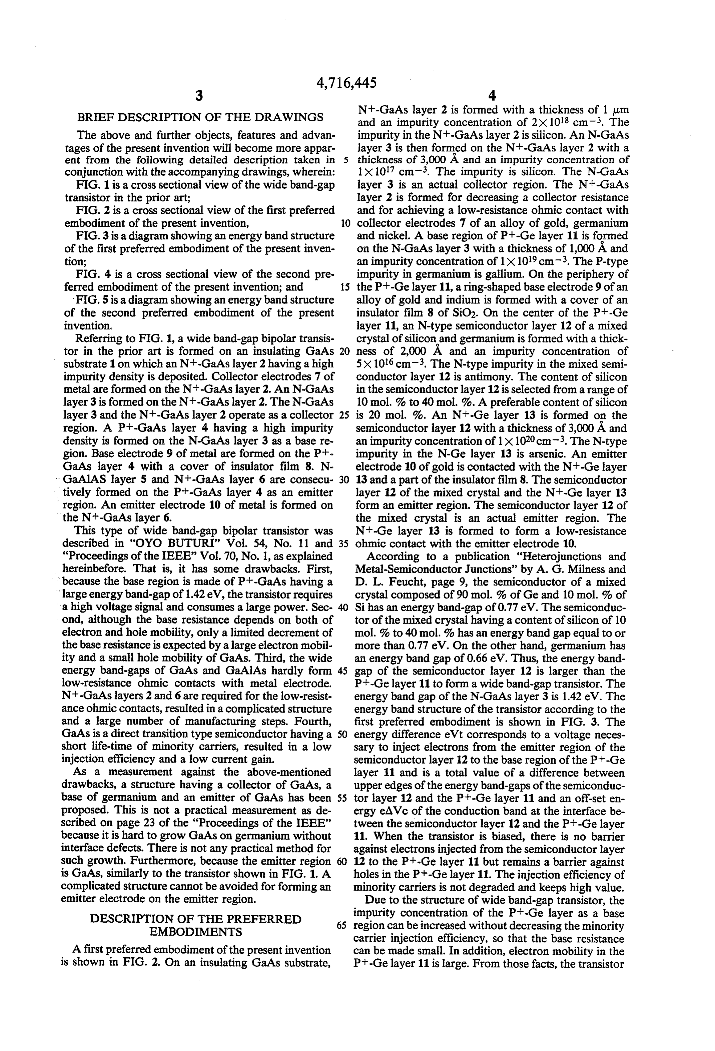
The above and further objects, features and advan impurity in the N-GaAs layer 2 is silicon. An N-GaAs tages of the present invention will become more appar layer 3 is then formed on the N+-GaAs layer 2 with a ent from the following detailed description taken in 5 thickness of 3,000 A and an impurity concentration of conjunction with the accompanying drawings, wherein: 1x1017 cm-3. The impurity is silicon. The N-GaAs FIG. 1 is a cross sectional view of the wide band-gap layer 3 is an actual collector region. The N-GaAs transistor in the prior art; layer 2 is formed for decreasing a collector resistance FIG. 2 is a cross sectional view of the first preferred and for achieving a low-resistance ohmic contact with embodiment of the present invention, 10 collector electrodes 7 of an alloy of gold, germanium FIG.3 is a diagram showing an energy band structure and nickel. A base region of P+-Ge layer 11 is formed of the first preferred embodiment of the present inven on the N-GaAs layer 3 with a thickness of 1,000 A and tion; an impurity concentration of 1 x 1019 cm3. The P-type FIG. 4 is a cross sectional view of the second pre impurity in germanium is gallium. On the periphery of ferred embodiment of the present invention; and the P-Gelayer 11, a ring-shaped base electrode 9 of an FIG. 5 is a diagram showing an energy band structure alloy of gold and indium is formed with a cover of an of the second preferred embodiment of the present insulator film 8 of SiO2. On the center of the P-Ge invention. layer 11, an N-type semiconductor layer 12 of a mixed Referring to FIG. 1, a wide band-gap bipolar transis crystal of silicon and germanium is formed with a thick tor in the prior art is formed on an insulating GaAs 20 ness of 2,000 A and an impurity concentration of substrate 1 on which an N-GaAs layer 2 having a high 5X1016 cm3. The N-type impurity in the mixed semi impurity density is deposited. Collector electrodes 7 of conductor layer 12 is antimony. The content of silicon metal are formed on the N-GaAs layer 2. An N-GaAs in the semiconductor layer 12 is selected from a range of layer 3 is formed on the N-GaAs layer 2. The N-GaAs 10 mol.% to 40 mol.%. A preferable content of silicon layer 3 and the N-GaAs layer 2 operate as a collector 25 is 20 mol. 7%. An N-F-Gelayer 13 is formed on the region. A P-GaAs layer 4 having a high impurity semiconductor layer 12 with a thickness of 3,000 A and density is formed on the N-GaAs layer 3 as a base re an impurity concentration of 1 x 1020 cm-3. The N-type gion. Base electrode 9 of metal are formed on the P impurity in the N-Ge layer 13 is arsenic. An emitter GaAs layer 4 with a cover of insulator film 8. N electrode 10 of gold is contacted with the N-F-Gelayer GaA1AS layer 5 and N-GaAs layer 6 are consecu 30 13 and a part of the insulator film 8. The semiconductor tively formed on the P-GaAs layer 4 as an emitter layer 12 of the mixed crystal and the N-F-Ge layer 13 region. An emitter electrode 10 of metal is formed on form an emitter region. The semiconductor layer 12 of the N-t-GaAs layer 6. the mixed crystal is an actual emitter region. The This type of wide band-gap bipolar transistor was N-Ge layer 13 is formed to form a low-resistance described in “OYO BUTURI” Vol. 54, No. 11 and 35 ohmic contact with the emitter electrode 10. "Proceedings of the IEEE' Vol. 70, No. 1, as explained According to a publication "Heterojunctions and hereinbefore. That is, it has some drawbacks. First, Metal-Semiconductor Junctions' by A. G. Milness and because the base region is made of P+-GaAs having a D. L. Feucht, page 9, the semiconductor of a mixed large energy band-gap of 1.42 eV, the transistor requires crystal composed of 90 mol.% of Ge and 10 mol.% of a high voltage signal and consumes a large power. Sec 40 Si has an energy band-gap of 0.77 eV. The semiconduc ond, although the base resistance depends on both of tor of the mixed crystal having a content of silicon of 10 electron and hole mobility, only a limited decrement of mol. 26 to 40 mol.% has an energy band gap equal to or the base resistance is expected by a large electron mobil more than 0.77 eV. On the other hand, germanium has ity and a small hole mobility of GaAs. Third, the wide an energy band gap of 0.66 eV. Thus, the energy band energy band-gaps of GaAs and GaAlAs hardly form 45 gap of the semiconductor layer 12 is larger than the low-resistance ohmic contacts with metal electrode. P-Gelayer 11 to form a wide band-gap transistor. The N-GaAs layers 2 and 6 are required for the low-resist energy band gap of the N-GaAs layer 3 is 1.42 eV. The ance ohmic contacts, resulted in a complicated structure energy band structure of the transistor according to the and a large number of manufacturing steps. Fourth, first preferred embodiment is shown in FIG. 3. The GaAs is a direct transition type semiconductor having a SO energy difference eVt corresponds to a voltage neces short life-time of minority carriers, resulted in a low sary to inject electrons from the emitter region of the injection efficiency and a low current gain. semiconductor layer 12 to the base region of the P+-Ge As a measurement against the above-mentioned layer 11 and is a total value of a difference between drawbacks, a structure having a collector of GaAs, a upper edges of the energy band-gaps of the semiconduc base of germanium and an emitter of GaAs has been 55 tor layer 12 and the P-Ge layer 11 and an off-set en proposed. This is not a practical measurement as de ergy eaVc of the conduction band at the interface be scribed on page 23 of the "Proceedings of the IEEE” tween the semiconductor layer 12 and the P+-Gelayer because it is hard to grow GaAs on germanium without 11. When the transistor is biased, there is no barrier interface defects. There is not any practical method for against electrons injected from the semiconductor layer such growth. Furthermore, because the emitter region 60 12 to the P-Ge layer 11 but remains a barrier against is GaAs, similarly to the transistor shown in FIG. 1. A holes in the P-Gelayer 11. The injection efficiency of complicated structure cannot be avoided for forming an minority carriers is not degraded and keeps high value. emitter electrode on the emitter region. Due to the structure of wide band-gap transistor, the DESCRIPTION OF THE PREFERRED impurity concentration of the P-Ge layer as a base 65 region can be increased without decreasing the minority
EMBODIMENTS
carrier injection efficiency, so that the base resistance
A first preferred embodiment of the present invention can be made small. In addition, electron mobility in the is shown in FIG. 2. On an insulating GaAs substrate, P-Gelayer 11 is large. From those facts, the transistor
Page 6
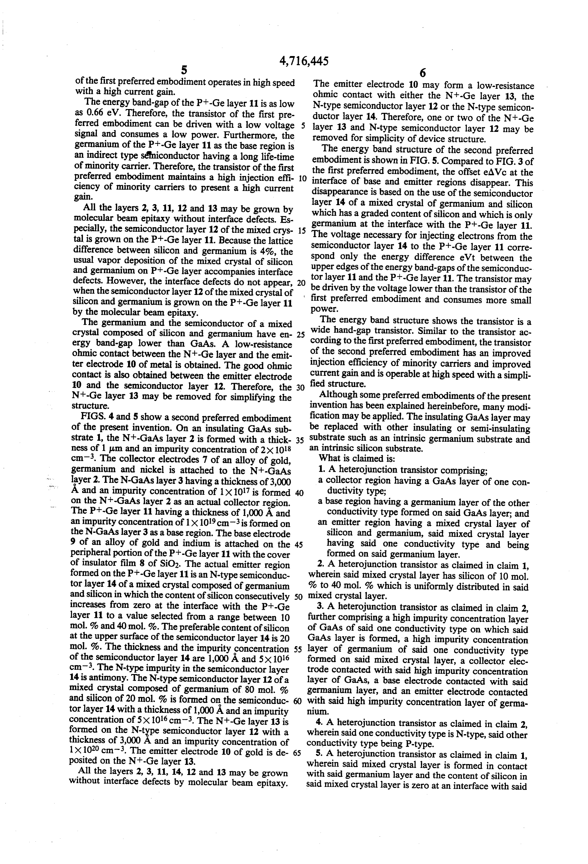
of the first preferred embodiment operates in high speed The emitter electrode 10 may form a low-resistance with a high current gain. ohmic contact with either the N-Ge layer 13, the The energy band-gap of the Pt-Gelayer 11 is as low N-type semiconductor layer 12 or the N-type semicon as 0.66 eV. Therefore, the transistor of the first pre ductor layer 14. Therefore, one or two of the N+-Ge ferred embodiment can be driven with a low voltage layer 13 and N-type semiconductor layer 12 may be signal and consumes a low power. Furthermore, the removed for simplicity of device structure. germanium of the Pt-Ge layer 11 as the base region is The energy band structure of the second preferred an indirect type sémiconductor having a long life-time embodiment is shown in FIG. 5. Compared to FIG.3 of of minority carrier. Therefore, the transistor of the first the first preferred embodiment, the offset eAVc at the preferred embodiment maintains a high injection effi 10 interface of base and emitter regions disappear. This ciency of minority carriers to present a high current disappearance is based on the use of the semiconductor gain.
All the layers 2, 3, 11, 12 and 13 may be grown by which layer 14 of a mixed crystal of germanium and silicon molecular beam epitaxy without interface defects. Es germanium has a graded content of silicon and which is only pecially, the semiconductor layer 12 of the mixed crys 15 at the interface with the P-Ge layer 11. tal is grown on the Pt-Gelayer 11. Because the lattice The voltage necessary for injecting electrons from the semiconductor layer 14 to the P+-Ge layer 11 corre difference between silicon and germanium is 4%, the spond only the energy difference eVt between the usual vapor deposition of the mixed crystal of silicon upper edges of the energy band-gaps of the semiconduc and germanium on P-Ge layer accompanies interface defects. However, the interface defects do not appear, 20 tor layer 11 and the P+-Gelayer 11. The transistor may when the semiconductor layer 12 of the mixed crystal of be driven by the voltage lower than the transistor of the silicon and germanium is grown on the P-Gelayer 11 power. first preferred embodiment and consumes more small by the molecular beam epitaxy.
The germanium and the semiconductor of a mixed The energy band structure shows the transistor is a crystal composed of silicon and germanium have en 25 wide hand-gap transistor. Similar to the transistor ac ergy band-gap lower than GaAs. A low-resistance cording to the first preferred embodiment, the transistor ohmic contact between the N-Gelayer and the emit of the second preferred embodiment has an improved ter electrode 10 of metal is obtained. The good ohmic injection efficiency of minority carriers and improved contact is also obtained between the emitter electrode current gain and is operable at high speed with a simpli 10 and the semiconductor layer 12. Therefore, the 30 fied structure.
N-Ge layer 13 may be removed for simplifying the Although some preferred embodiments of the present structure. invention has been explained hereinbefore, many modi FIGS. 4 and 5 show a second preferred embodiment fication may be applied. The insulating GaAs layer may of the present invention. On an insulating GaAs sub be replaced with other insulating or semi-insulating strate 1, the N-GaAs layer 2 is formed with a thick 35 substrate such as an intrinsic germanium substrate and ness of 1 am and an impurity concentration of 2X 10¹⁸ an intrinsic silicon substrate.
cm3. The collector electrodes 7 of an alloy of gold, What is claimed is:
germanium and nickel is attached to the N-GaAs 1. A heterojunction transistor comprising; layer 2. The N-GaAs layer 3 having a thickness of 3,000 a collector region having a GaAs layer of one con ductivity type;
A and an impurity concentration of 1x10¹⁷ is formed on the N-GaAs layer 2 as an actual collector region. a base region having a germanium layer of the other The P-Gelayer 11 having a thickness of 1,000 A and conductivity type formed on said GaAs layer; and an impurity concentration of 1 x 1019 cm-3 is formed on an emitter region having a mixed crystal layer of the N-GaAs layer 3 as a base region. The base electrode silicon and germanium, said mixed crystal layer 9 of an alloy of gold and indium is attached on the 45 having said one conductivity type and being peripheral portion of the P+-Gelayer 11 with the cover formed on said germanium layer. of insulator film 8 of SiO2. The actual emitter region 2. A heterojunction transistor as claimed in claim 1, formed on the P-Gelayer 11 is an N-type semiconduc wherein said mixed crystal layer has silicon of 10 mol. tor layer 14 of a mixed crystal composed of germanium % to 40 mol. 26 which is uniformly distributed in said and silicon in which the content of silicon consecutively 50 mixed crystal layer.
increases from zero at the interface with the P-Ge 3. A heterojunction transistor as claimed in claim 2, layer 11 to a value selected from a range between 10 further comprising a high impurity concentration layer mol.% and 40 mol.%. The preferable content of silicon of GaAs of said one conductivity type on which said at the upper surface of the semiconductor layer 14 is 20 GaAs layer is formed, a high impurity concentration mol%. The thickness and the impurity concentration 55 layer of germanium of said one conductivity type of the semiconductor layer 14 are 1,000 A and 5X10¹⁶ formed on said mixed crystal layer, a collector elec cm3. The N-type impurity in the semiconductor layer trode contacted with said high impurity concentration 14 is antimony. The N-type semiconductor layer 12 of a layer of GaAs, a base electrode contacted with said mixed crystal composed of germanium of 80 mol. 9% germanium layer, and an emitter electrode contacted and silicon of 20 mol % is formed on the semiconduc with said high impurity concentration layer of germa tor layer 14 with a thickness of 1,000 A and an impurity nium.
concentration of 5x1016 cm-3. The N+-Gelayer 13 is 4. A heterojunction transistor as claimed in claim 2, formed on the N-type semiconductor layer 12 with a wherein said one conductivity type is N-type, said other thickness of 3,000 A and an impurity concentration of conductivity type being P-type.
1X 1020 cm-3. The emitter electrode 10 of gold is de 65 5. A heterojunction transistor as claimed in claim 1, posited on the N-Ge layer 13. wherein said mixed crystal layer is formed in contact All the layers 2, 3, 11, 14, 12 and 13 may be grown with said germanium layer and the content of silicon in without interface defects by molecular beam epitaxy. said mixed crystal layer is zero at an interface with said
Page 7
germanium layer and is continuously increased with a a second germanium layer of said one conductivity distance from said interface. type formed in contact with said semiconductor 6. A heterojunction transistor as claimed in claim 5, layer; and wherein a maximum value of said content of silicon is a an emitter electrode coupled to said second germa value between 10 mol. 2% and 40 mol. 26. 5 nium layer.
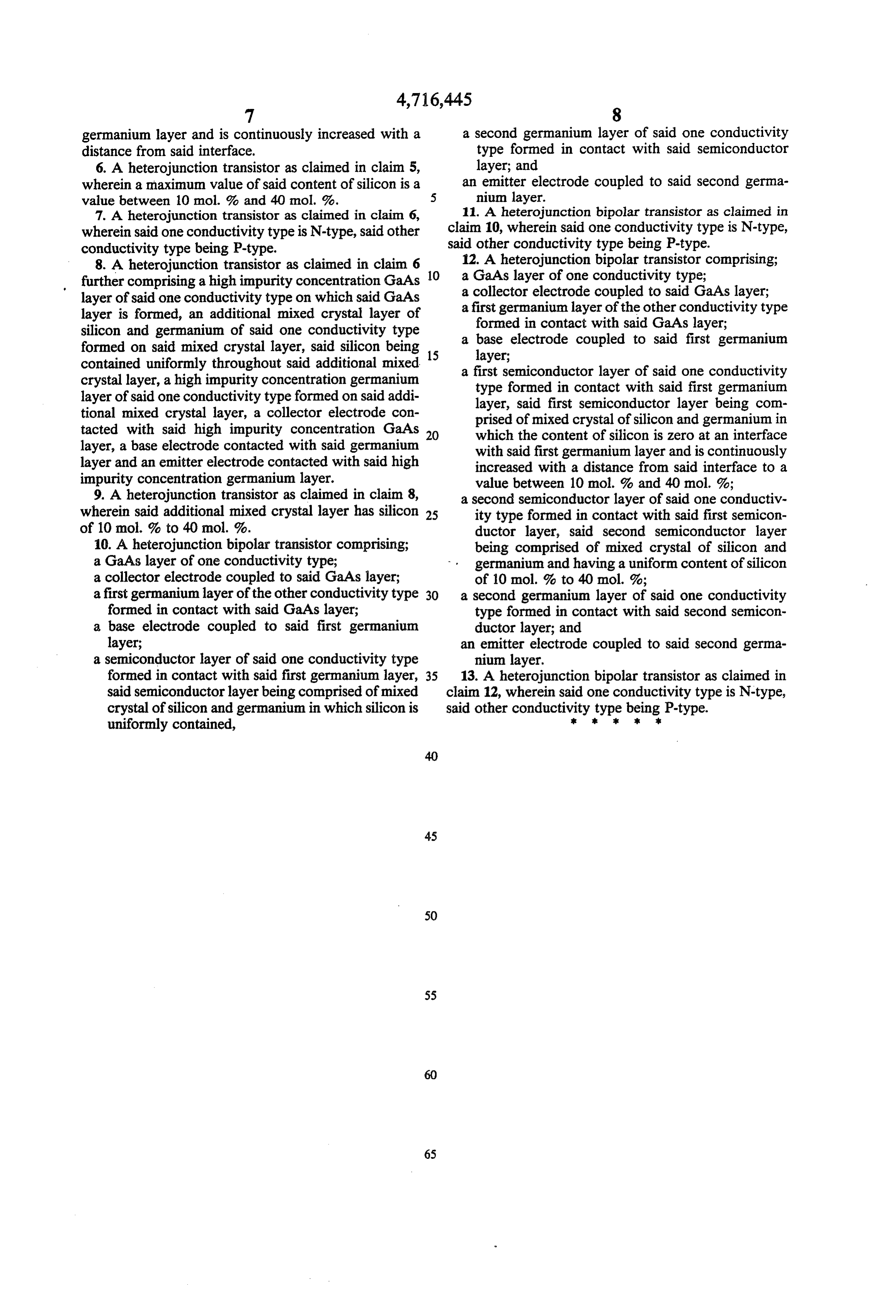
7. A heterojunction transistor as claimed in claim 6, 11. A heterojunction bipolar transistor as claimed in wherein said one conductivity type is N-type, said other claim 10, wherein said one conductivity type is N-type, conductivity type being P-type. said other conductivity type being P-type. 8. A heterojunction transistor as claimed in claim 6 12. A heterojunction bipolar transistor comprising; further comprising a high impurity concentration GaAs O aa collector
GaAs layer of one conductivity type;
electrode coupled to said GaAs layer;
layer of said one conductivity type on which said GaAs a first germanium layer of the other conductivity type layer is formed, an additional mixed crystal layer of formed in contact with said GaAs layer; silicon and germanium of said one conductivity type formed on said mixed crystal layer, said silicon being 15 a base layer;
electrode coupled to said first germanium contained uniformly throughout said additional mixed a first semiconductor layer of said one conductivity crystal layer, a high impurity concentration germanium type formed in contact with said first germanium layer of said one conductivity type formed on said addi layer, said first semiconductor layer being con tional mixed crystal layer, a collector electrode con prised of mixed crystal of silicon and germanium in tacted with said high impurity concentration GaAs 20 which the content of silicon is zero at an interface layer, a base electrode contacted with said germanium with said first germanium layer and is continuously layer and an emitter electrode contacted with said high increased with a distance from said interface to a impurity concentration germanium layer. value between 10 mol. 2 and 40 mol. 26; 9. A heterojunction transistor as claimed in claim 8, a second semiconductor layer of said one conductiv wherein said additional mixed crystal layer has silicon 25 ity type formed in contact with said first semicon of 10 mol. 9% to 40 mol. 2%. ductor layer, said second semiconductor layer 10. A heterojunction bipolar transistor comprising; being comprised of mixed crystal of silicon and a GaAs layer of one conductivity type; germanium and having a uniform content of silicon a collector electrode coupled to said GaAs layer; of 10 mol.% to 40 mol.%;
a first germanium layer of the other conductivity type 30a second germanium layer of said one conductivity formed in contact with said GaAs layer; type formed in contact with said second semicon a base electrode coupled to said first germanium ductor layer; and layer; an emitter electrode coupled to said second germa a semiconductor layer of said one conductivity type nium layer.
formed in contact with said first germanium layer, 35 13. A heterojunction bipolar transistor as claimed in said semiconductor layer being comprised of mixed claim 12, wherein said one conductivity type is N-type, crystal of silicon and germanium in which silicon is said other conductivity type being P-type. uniformly contained, is : : :
Page 8
UNITED STATES PATENT AND TRADEMARK OFFICE
CERTIFICATE OF CORRECTION
INVENTOR(S); SONE
it is certified that error appears in the above-identified patent and that said letters Patent is hereby corrected as shown below:
COLUMN 1, LINE 65 Delete "Ce" and insert --Ge. --
Signed and Sealed this
Twenty-third Day of August, 1988
Attest:
DONALD J. QUIGG
Attesting Officer Commissioner of Patents and Trademarks
Provenance
- Collection
- Cited prior art
- Original PDF
- patentimages.storage.googleapis.com →
- Filed
- 1987-01-20
- Pages
- 8
- Method
- pdftotext (the PDF's own text layer) + pdftoppm 300dpi page scans
- Source
- Google Patents bibliographic record
- Granted
- 1987-12-29
- Inventors
- Jun'ichi Sone; NEC Corp
- Transcribed from
- patentimages.storage.googleapis.com →