patent · US5780727
Electromechanical transducer
14 July 1998
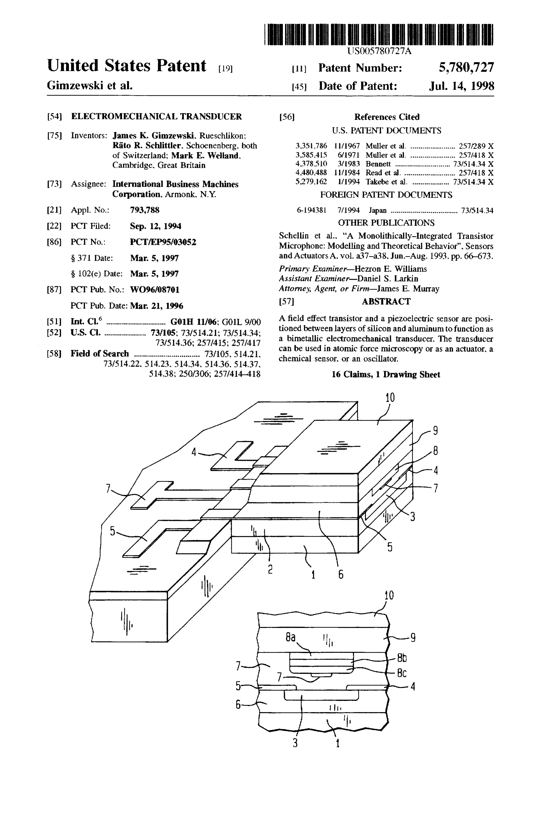
Page 1 — bibliographic record
United States Patent (19) 11 Patent Number: 5,780,727 Gimzewski et al. 45 Date of Patent: Jul. 14, 1998 54 ELECTROMECHANICAL TRANSDUCER 56) References Cited
(75) Inventors: James K. Gimzewski. Rueschlikon;
Rato R. Schlittler. Schoenenberg, both 3.351,786 l/1967 Muller et al. ....................... 257/.289 X of Switzerland; Mark E. Welland, 3.585,45 671971 Muller et al. ....................... 257/418 X Cambridge. Great Britain 4,378,50 3,983 Bennett ........ ... 73/5434 X 4.430,488 f984 Read et al. ...... ....... 257/418 X 73) Assignee: International Business Machines 5,279, 62 fl994 Takebe et al. ................... 73/51.34 X Corporation. Armonk, N.Y. FOREIGN PATENT DOCUMENTS 21 Appl. No.: 793,788 6-19438E 7/1994 Japan .................................. 73/S14.34 22 PCT Fed: Sep. 12, 1994 OTHER PUBLICATIONS
Schellin et al., "A Monolithically-Integrated Transistor
Microphone: Modelling and Theoretical Behavior". Sensors
S371 Date: Mar. 5, 1997 and Actuators A. vol. a7-a38. Jun.-Aug. 1993, pp. 66–673. S 102(e) Date: Mar. 5, 1997 Primary Examiner-Hezron E. Williams
Assistant Examiner-Daniel S. Larkin 87) PCT Pub. No.: WO96/08701 Attorney, Agent, or Firm-James E. Murray PCT Pub. Date: Mar 21, 1996 57 ABSTRACT 51 Int. Cl. .................... GOH 1/06: GOL 9/OO A field effect transistor and a piezoelectric sensor are posi (52) U.S. Cl. ..................... 73/105: 73/514.21; 73/514.34; tioned between layers of silicon and aluminum to function as 73/514.36; 257/415; 257/417 a bimetallic electromechanical transducer. The transducer 58 Field of Search .............................. 7.3/105,54.21, can be used in atomic force microscopy or as an actuator, a chemical sensor, or an oscillator,
51438: 250/306; 257/414418 16 Claims, 1 Drawing Sheet
Page 2
Drawing sheet — no readable text.
Page 3
ELECTROMECHANCAL TRANSDUCER Another attempt to produce small Integrated cantilevers for atomic force microscopy Is known from: M. Tortonese et
The present invention relates to an electromechanical al., Appl. Phys. Lett. 62 (8). 22. Feb. 1993, pp. 834-836. The transducer comprising a flexible element and an annplifier, described bending detection scheme uses a piezoresistive wherein the transducer generates an electrical output in strain sensor. The deflection of the cantilever can be mea sympathy with the movement of the flexible element. The sured directly from the resistivity of a piezoresistive layer present invention also relates such a transducer employed as within the cantilever beam. This resistivity is determined by a cantilever in local probe microscopes, as sensors, or as an external Wheatstone bridge. The base material silicon oscillators. itself serves as the piezoresistive layer. In the European BACKGROUND OF THE INVENTION 10 patent application EP-A-0 290 647, the deflection of the cantilever is measured by attaching a piezoelectric oscillator
Electromechanical transducers are found In a broad range to the cantilever and determining the shift of frequency of technical fields. They are applied as parts of oscillating occurring when the cantilever is subject to a force gradient. circuits. vibrators, sensors, microactuators, or local probe Using this principle, K. Takata presents in the Rev. Sci. devices, such as the atomic force microscope (AFM). The 15 Instrum. 64 (9), Sept. 93, pp. 2598-2600 a device with a following presents a variety of known devices taken from piezoelectric vibrator Incorporated into the cantilever. By different technical fields. These devices emphasize the broad forming the vibrator as a bimorphous cantilever for an AFM, applicability of electromechanical transducers. the tip-to-sample spacing and the force gradient can be An integrated force sensor is described by R. H. Taylor detected simultaneously. As is apparent from the prior art. in and D. J. Webb in IBM's Technical Disclosure Bulletin, Vol. several fields attempts have been made to fabricate cantile 25. No. 12, May 1983 on pages 6424/5. This sensor consists vers for local probe techniques, as well as other sensors and of a piezoelectric layer coupled to an elongated gate of an oscillators in an integrated manner. However, all known associated field-effect transistor. Pressure on the piezoelec proposals still heavily depend on external circuitry which tric layer charges the gate electrode and thus modulates the make up for a large fraction of the size and complexity of the channel conductance of the field-effect transistor. 25 described devices. These devices require accurate alignment Another known device is presented by H. C. Nathanson et and additional wiring. Therefore. It is the object of the al. in the IEEE Transactions on Electron Devices. Wol. present Invention to provide a electromechanical transducer ED-14. No. 3, March 1967, pp. 117-133, as "resonant gate with a high degree of integration. It is a more specific object transistor (RGT)". The RGT employs a beam-shaped elec of the present invention to provide a robust transducer which trode suspended over the drain and source of a MOS-type 30 can readily be Introduced Into larger devices. A further field effect transistor. The oscillations of the (charged) beam object of the invention concerns highly Integrated cantilever vary the channel of the transistor. With an appropriate structures for local probe microscopy, sensors, actuators, feedback circuit, the RGT can be forced to oscillate with a and oscillators allowing for better control, especially of constant frequency. bending and deflection.
The use of an electromechanical transducer as a "dual 35 direction switch' is demonstrated in U.S. Pat, No. 5,034, SUMMARY OF THE INVENTION 648. In this document a piezoelectric rod is attached to the In accordance with the present invention the transducer of gates of two field-effect transistors. this invention comprises a flexible element incorporating an A piezoelectric actuator for micromechanical devices is essential part of an amplifying circuit. With the exception of further described in Sensors and Actuators, A21-A23 40 an external power supply, the amplifying circuit is com (1990), pp. 226-228 by F. R. Blom et al. The actuator is pletely incorporated into the flexible element. In a preferred formed by a multilayered cantilever which consists of a SiO, embodiment, this amplifying circuit is a field-effect transis layer and a ZnO layer. both sandwiched between two metal tor wherein a small gate voltage is used to control the current layers. Any voltage applied to the metal layers gives rise to flowing from source to drain. The preferred dimensions of a deflection of the cantilever. Unimorphous or bimorphous 45 the flexible element range in case of highly sensitive devices piezoelectric cantilevers have also found entry in the field of from 1 mm to down to 1 micron in either direction. The atomic force microscopy (AFM). Atomic force microscopy amplifying circuit is advantageously fabricated using to thin is a specific variant of the so-called "local probe methods". film transistor (TFT) technology. Thin film transistors are all of which involve the use of a tip with an apex having a basically analogous to metal-oxide semiconductor field curvature in the range of 10 to 100 nm. The tip or probe is 50 effect transistors (MOSFETs) but whereas high quality brought into proximity of a sample to be investigated by single crystal substrates (wafers) are used for MOSFETs, all means of piezoelectric transducers. In AFM and related components in TFTs can be deposited onto an insulating techniques, the tip is attached to a piezoelectric cantilever. substrate, for example SiN. SiO, SiON. TaO. AlO3, or Numerous proposals are known to exploit the piezoelectric composite layers. Advantageously, the base material of the material of the cantilever in order to control its deflection 55 flexible element or oxides of this material are used as a when approaching the surface to the sample. Examples of substrate for the TFT device. In case the amplifying device these proposals are found in the European patent application to be incorporated into the flexible element is a FET, at least EP-A-0 492 915, showing several ways of producing can a source, a drain, and a gate electrode has to be deposited tilever probes with several piezoelectric layers and an appro onto the substrate. Suitable electrodes are made of conduct priate number of electrodes to apply a voltage to the piezo ing material, in particular metals, such as Au, Al, Mo, Ta Ti, electric layers. U.S. Pat. No. 4,906,840 discloses a similarly ITO (indium-tin oxide). NiCr, or Cu being deposited by layered cantilever structure with a piezoelectric bimorphous evaporation and photoetching, or other techniques. To insu layer allowing the cantilever beam to be bent in opposite late the gate electrode from the semiconducting channel directions from its rest position. In some embodiments, the which connects drain and source, the same dielectric mate control circuitry necessary to load the piezoelectric bimorph 65 rials as mentioned above as base materials for substrates are is proposed to be integrated into the substrate from which the applicable. These layers can be deposited by evaporation, cantilever is etched. sputtering, chemical vapor deposition (CVD), molecular
Page 4
beam epitaxy (MBE), or the like. Provided a suitable metal fier stage being part of the cantilever structure. The energy is used as the gate electrode, the Insulating layer may also dissipation and noise limitations are reduced. Further, when be produced by causing anodic oxidation to this electrode. comparing the new cantilever with other known AFM The semiconducting channel itself can be based on materials techniques, complex. macroscopic read-out devices or including Si, a-Si:H. poly-Si. CdSe, Te, In, Sb, or Ge. For detectors, in many cases optical devices, for measuring the specific areas, such as the ohmic contact to the source or deflection of the cantilever are avoided. In another preferred drain electrode. n+ doped a-Si:H or doping with barrier embodiment of this aspect of the invention, the flexible metals might be considered. These materials are deposited element includes at least two layers with different thermal by evaporation, sputtering. CVD. MBE. or by other known expansion coefficients. Thus, a temperature change causes a deflection of the flexible element in a fashion known as techniques. The layer is patterned by either photolithogra “bimetal" effect. When the thermal expansion coefficients of phy with etching, plasma etching, or ion beam milling. It is the two layers differs by at least a factor of ten, even small also feasible to use a lithographic process which involves a temperature changes can be monitored. The applicability of scanning probe microscope. this "bimetal" variant of the invention can be enlarged by As a further aspect of the invention, the flexible element 15 including chemically active layer, for example a catalyst or also incorporates voltage generating means, preferably an absorbing layer, as described in the international appli piezoelectric elements. These elements form either a single cation PCT/EP93/01742. Any heat dissipation due to a layer (unimorph) or a combination of two (bimorph) or chemical reaction at the chemical active layer is transduced several layers (multimorph). Thus, the voltage generating via the displacement of the flexible element into a detectable means can be tailored so as to produce a voltage when being electrical signal. The sensitivity range of this cantilever elongated, compressed, stressed, or strained. Preferred structure spans into the nano- and even into the picowatt piezoelectric materials include ZnO, AIN. and PZT, which region.
can be sputtered onto the base material. Other piezoelectric The "bimetal" variant of the Invention Isfurther improved materials. In particular polymers, such as polyvenylidene by providing means for a heat calibration. This heat cali fluoride (PVDF) or copolymers thereof, can be applied if bration Is achieved by a resistive heating element, preferably bonded to the substrate by an adhesive material or a suitable 25 a loop of a conducting material deposited onto the flexible glue. element. With the resistance of the loop known, a defined The flexible element of this Invention is characterized by amount device of heat can be applied-to the flexible element. The is calibrated by measuring the deflection caused by having elastic properties (spring constant) and by being able to perform a bending or oscillatory movement. Examples of different amounts of heat.
the flexible elements are cantilever structures as found in the The resistive heating element can also be used to perform atomic force microscopy, or thin membranes used for vari thermal ab-fciesorption studies of molecules. ous applications. For reasons of compatibility with the As the present invention can be based on standard silicon existing integrated circuit technology, preferred base mate and TFT technology, a mass production of devices according rials include silicon or silicon nitride and their respective 35 to this invention is readily feasible. By combining silicon oxides. Flexible elements are produced by anisotropic etch micromachining, described for example by K. E. Petersen in ing with alkaline solutions, such as KOH (potassium the IEEE Transaction on Electron Devices, Vol. ED-25, No. hydroxide). solutions of EDP (ethylenediamin, 10, pp. 1241-1249, with the technology applied to produce pyrocatechol, and water), solutions of hydracine, or solu TFT displays, large arrays of devices according to the tions based on ammoniumhydroxide or tetramethyl ammo current invention can be manufactured to provide touch or niumhydroxide and water. heat sensitive screens and panels. The robustness of silicon Using an integrated device comprising a flexible element, guarantees a long lifetime and a sufficient protection against voltage generating means and an electronic amplifier, output physical destruction. Another standard material which may signals between 1V and 5V are generated for displacements be tion applied to manufacture a device according to this inven may be gallium arsenide and its alloys, e.g. AlGaAs.
of the flexible element well below one nanometer. In 45
Processing techniques for this material are described for operation, the voltage generating means produces a voltage example depending on the amount of deflection or bending of the In J. Micromech. Microeng. 4 (1994), p. 1-13 by flexible element. This voltage modulates either the electrical K.These
Hjort et al.
and other novel features believed to be character field and in sympathy the source-drain current, or drives the base current in case of a base collector amplifier. istic of the invention are set forth in the appended claims. Referring to a further aspect of the invention, advanta The use, invention itself however, as well a preferred mode of and further objects and advantageous thereof, will best geously the amplifying means are protected against any peak be understood by reference to the following detailed descrip voltage potentially produced by the piezoelectric elements. tion of illustrative embodiments when read in conjunction Suitable protection can be provided by a bias voltage applied with the accompanying drawings. to the gate electrode or in, two terminal devices (diodes) 55 having a fixed breakthrough voltage integrated into the DESCRIPTION OF THE DRAWINGS flexible element (integrated protection diode), voltage The invention is described in detail below with reference divider, etc. to the following drawings:
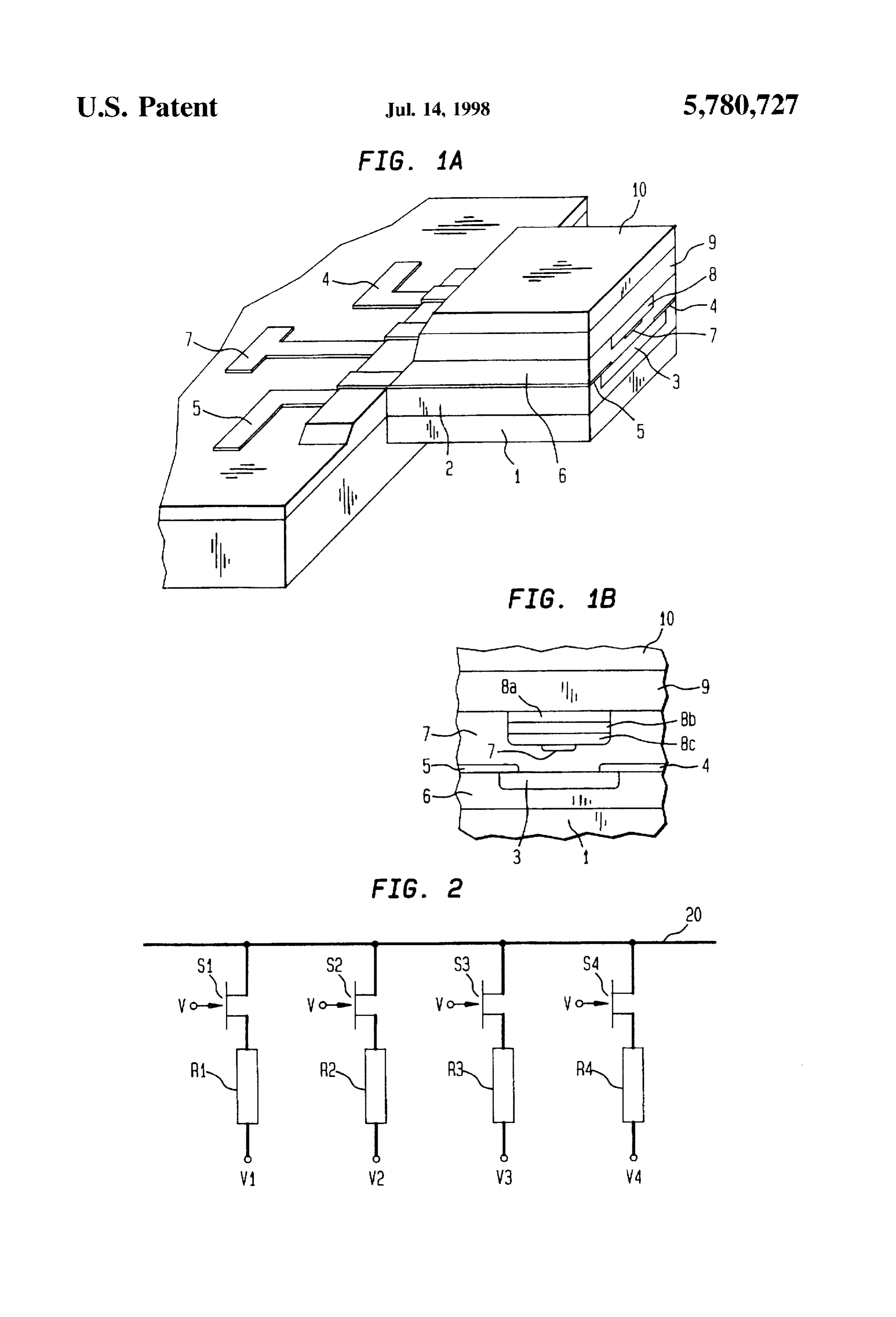
As another aspect of the Invention, the flexible element FIGS. 1a and 1b show a silicon based micromechanical acts as a transducer which translates other physical cantilever in accordance with this invention. properties, such as force. heat, and light intensity into a FIG. 2 depicts schematically an array of devices in displacement. In a preferred embodiment of this aspect of accordance with the current invention.
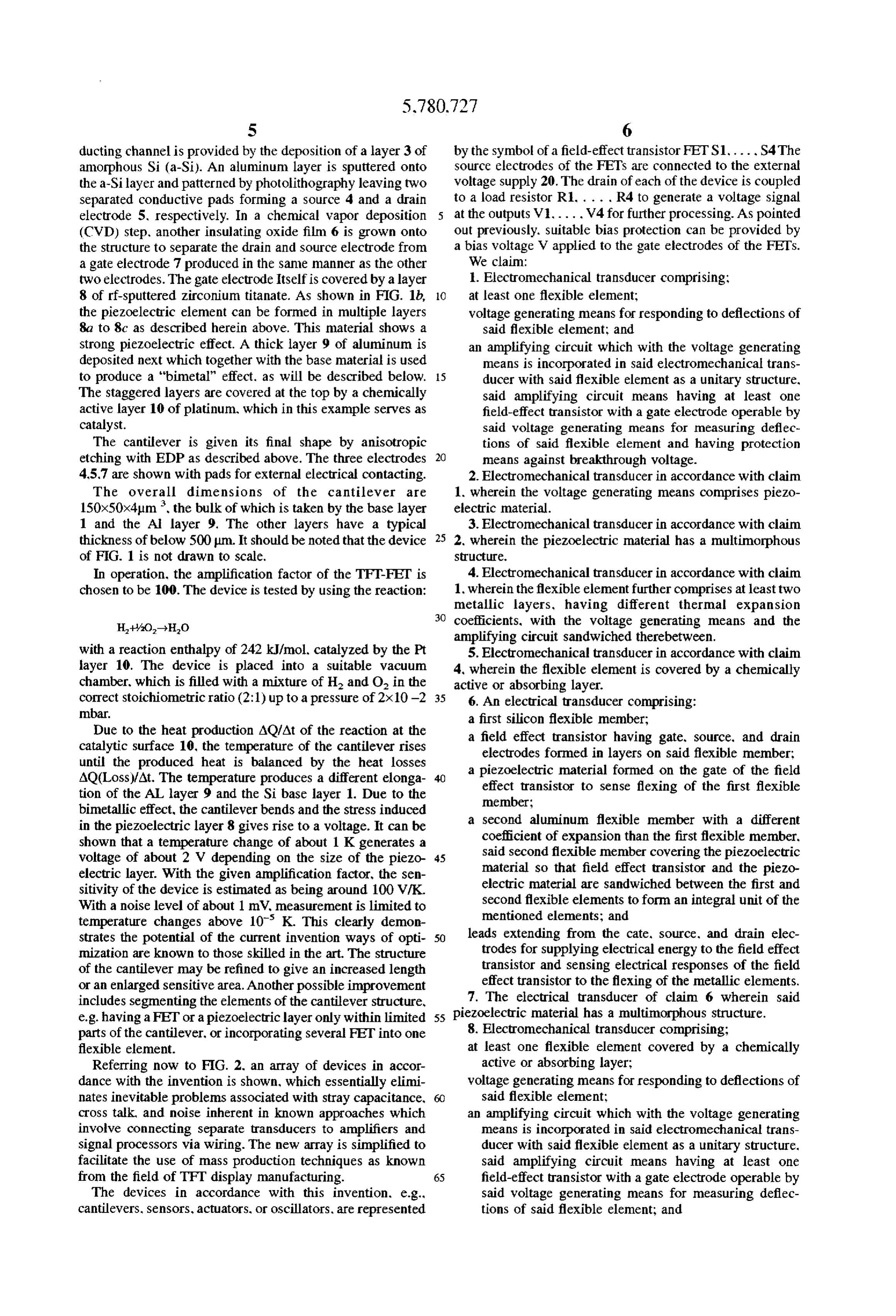
the invention, a tip Is attached to the flexible element to give an improved sensor for local probe devices, as are defined MODE(S) FOR CARRYING OUT THE above. Compared to known AFM techniques, such as the 65 NVENTION above-mentioned piezoresistive cantilever, this embodiment Referring now to FIG. 1, an insulating layer 2 of SiO, is provides a higher degree of integration with the first ampli grown on a base material comprising Si. Next, a semicon
Page 5
S 6 ducting channel is provided by the deposition of a layer 3 of by the symbol of a field-effect transistor FETS1,..., S4. The amorphous Si (a-Si). An aluminum layer is sputtered onto source electrodes of the FETs are connected to the external the a-Silayer and patterned by photolithography leaving two voltage supply 20. The drain of each of the device is coupled separated conductive pads forming a source 4 and a drain to a load resistor R1. . . . . R4 to generate a voltage signal electrode 5, respectively. In a chemical vapor deposition 5 at the outputs V1. . . . . V4 for further processing. As pointed (CVD) step, another insulating oxide film 6 is grown onto out previously. Suitable bias protection can be provided by the structure to separate the drain and source electrode from a bias voltage V applied to the gate electrodes of the FETs. a gate electrode 7 produced in the same manner as the other We claim:
two electrodes. The gate electrode Itself is covered by a layer 1. Electromechanical transducer comprising: 8 of rf-sputtered zirconium titanate. As shown in FIG. 1b, 10 at least one flexible element;
the piezoelectric element can be formed in multiple layers voltage generating means for responding to deflections of 8a to 8c as described herein above. This material shows a said flexible element; and strong piezoelectric effect. A thick layer 9 of aluminum is an amplifying circuit which with the voltage generating deposited next which together with the base material is used means is incorporated in said electromechanical trans to produce a "bimetal" effect. as will be described below. 15 ducer with said flexible element as a unitary structure, The staggered layers are covered at the top by a chemically said amplifying circuit means having at least one active layer 10 of platinum, which in this example serves as field-effect transistor with a gate electrode operable by catalyst. said voltage generating means for measuring deflec The cantilever is given its final shape by anisotropic tions of said flexible element and having protection etching with EDP as described above. The three electrodes 2O means against breakthrough voltage. 45.7 are shown with pads for external electrical contacting. 2. Electromechanical transducer in accordance with claim The overall dimensions of the cantilever are 1, wherein the voltage generating means comprises piezo 150x50x4.um, the bulk of which is taken by the base layer electric material.
1 and the Al layer 9. The other layers have a typical 3. Electromechanical transducer in accordance with claim thickness of below 500 m. It should be noted that the device 25 2, wherein the piezoelectric material has a multimorphous of FIG. 1 is not drawn to scale. Structure.
In operation, the amplification factor of the TFT FET is 4. Electromechanical transducer in accordance with claim chosen to be 100. The device is tested by using the reaction: 1, wherein the flexible element further comprises at least two metallic layers, having different thermal expansion 30 coefficients, with the voltage generating means and the amplifying circuit sandwiched therebetween.
with a reaction enthalpy of 242 kJ/mol, catalyzed by the Pt 5. Electromechanical transducer in accordance with claim layer 10. The device is placed into a suitable vacuum 4, wherein the flexible element is covered by a chemically chamber, which is filled with a mixture of H and O in the active or absorbing layer.
correct stoichiometric ratio (2:1) up to a pressure of 2x10⁻² 3. 6. An electrical transducer comprising: mbar. a first silicon flexible member; Due to the heat production AQ/At of the reaction at the a field effect transistor having gate, source, and drain catalytic surface 10, the temperature of the cantilever rises electrodes formed in layers on said flexible member; until the produced heat is balanced by the heat losses a piezoelectric material formed on the gate of the field AQ(Loss)/At. The temperature produces a different elonga tion of the AL layer 9 and the Si base layer 1. Due to the 40 effect transistor to sense flexing of the first flexible member;
bimetallic effect, the cantilever bends and the stress induced in the piezoelectric layer 8 gives rise to a voltage. It can be a second aluminum flexible member with a different shown that a temperature change of about 1 K generates a coefficient of expansion than the first flexible member, voltage of about 2 V depending on the size of the piezo 45 said second flexible member covering the piezoelectric electric layer. With the given amplification factor, the sen material so that field effect transistor and the piezo sitivity of the device is estimated as being around 100 V/K. electric material are sandwiched between the first and With a noise level of about 1 mV, measurement is limited to second flexible elements to form an integral unit of the temperature changes above 10 K. This clearly demon mentioned elements; and strates the potential of the current invention ways of opti so leads extending from the cate, source, and drain elec mization are known to those skilled in the art. The structure trodes for supplying electrical energy to the field effect of the cantilever may be refined to give an increased length transistor and sensing electrical responses of the field or an enlarged sensitive area. Another possible improvement effect transistor to the flexing of the metallic elements. includes segmenting the elements of the cantilever structure, 7. The electrical transducer of claim 6 wherein said e.g. having a FET or a piezoelectric layer only within limited ss piezoelectric material has a multimorphous structure. parts of the cantilever, or incorporating several FET into one 8. Electromechanical transducer comprising: flexible element. at least one flexible element covered by a chemically Referring now to FIG. 2. an array of devices in accor active or absorbing layer;
dance with the invention is shown, which essentially elimi voltage generating means for responding to deflections of nates inevitable problems associated with stray capacitance, 60 said flexible element:
cross talk, and noise inherent in known approaches which an amplifying circuit which with the voltage generating involve connecting separate transducers to amplifiers and means is incorporated in said electromechanical trans signal processors via wiring. The new array is simplified to ducer with said flexible element as a unitary structure. facilitate the use of mass production techniques as known said amplifying circuit means having at least one from the field of TFT display manufacturing. 65 field-effect transistor with a gate electrode operable by The devices in accordance with this invention, e.g. said voltage generating means for measuring deflec cantilevers, sensors, actuators, or oscillators, are represented tions of said flexible element; and
Page 6
at least two metallic layers in said flexible element, said a second flexible member covering the piezoelectric mate two metallic layers having different thermal expansion rial so that field effect transistor including the gate. coefficients and having the voltage generating means drain, and source electrodes and the piezo electric and the amplifying circuit sandwiched therebetween. material are sandwiched between the first and second 9. Electromechanical transducer in accordance with claim 5 8, wherein the voltage generating means comprises piezo flexible elements to form an integral cantilever unit of electric material. the mentioned elements that extends out from said 10. Electromechanical transducer in accordance with body.
claim 9, wherein the piezoelectric material has a multimor 13. The electrical transducer of claim 12 wherein the first phous structure. O 11. Electromechanical transducer in accordance with and second flexible members are metallic with different claim 8, wherein the transistor further comprises protection coefficients of thermal expansion to provide a bimetal effect means against break-through voltage. to bend the cantilever unit in response to temperature 12. An electrical transducer comprising: changes to produce a voltage from the transducer.
a body of the electrical transducer; 14. The electrical transducer of claim 12 wherein one of a first flexible member extending out from the body of the said flexible members is silicon and the other is aluminum. electrical transducer;
a field effect transistor having gate source, and drain 15. The electrical transducer of claim 13 including a electrodes and an insulating layer between the gate, chemically active or absorbing layer which generates heat source, and drain electrodes formed in layers on said over the second flexible member.
flexible member: 16. The electrical transducer of claim 12 wherein said a piezoelectric material formed on the gate of the field electrical transducer is a microscope probe. effect transistor to sense flexing of the first flexible member, and xk : k
Provenance
- Collection
- Cited prior art
- Original PDF
- patentimages.storage.googleapis.com →
- Filed
- 1994-09-12
- Pages
- 6
- Method
- pdftotext (the PDF's own text layer) + pdftoppm 300dpi page scans
- Source
- Google Patents bibliographic record
- Granted
- 1998-07-14
- Inventors
- James K. Gimzewski; Rato R. Schlittler; Mark E. Welland; International Business Machines Corp
- Transcribed from
- patentimages.storage.googleapis.com →