patent · US5488231
Metal/semiconductor junction Schottky diode optical device using a distortion grown layer
30 January 1996
Page 1 — bibliographic record
IIIHIIIHIIIHIII
United States Patent (19) 11 Patent Number: 5,488,231 Kwon et al. (45) Date of Patent: Jan. 30, 1996 54 METAL/SEMICONDUCTOR JUNCTION 5,053,843 10/1991 Choudhury et al. ...................... 257/21 SCHOTTKY DIODE OPTICAL DEVICE 5,233,184 8/1993 Chirovsky et al. ............... 250/214 LS USING A DISTORTION GROWN LAYER FOREIGN PATENT DOCUMENTS 75 Inventors: O-Kyun Kwon, Daejeon; Young-Wan 0249645 12/1987 European Pat. Off. ................ 257/21 Choi, Seoul, El-Hang Lee, Daejeon, all 2199877 8/1990 Japan ....................................... 257/21 of Rep. of Korea 4.015367 7/1994 WIPO .......... ... 257/449
73) Assignee: Electronics and Telecommunications Primary Examiner-William Mintel Research Institute, Daejeon-shi, Rep. Attorney, Agent, or Firm-Antonelli, Terry, Stout & Kraus of Korea
21 Appl. No. 352,628 A metal/semiconductor junction Schottky diode optical device using a distortion grown layer is described. A plu 22 Filed: Dec. 9, 1994 rality of GaAs mirror and AlAs mirror layers are periodi 30 Foreign Application Priority Data cally grown on a semi-insulating GaAs substrate. An n- or p+ semiconductor layer is formed on the GaAs mirror and
Nov. 23, 1994 (KR) Rep. of Korea ...................... 94-30898 AlAs mirror layers. A GaAs buffer layer is formed on the (51) Int. Cl. ............................. H01L 27/14; H01L 31/00 semiconductor layer to grow a Schottky metal layer serving 52 U.S. Cl. ................................. 257/17; 257/18: 257/21; as an electrode and a mirror. A multiple quantum well 257/432; 257/453; 257/455 structure having an electro-optical absorption characteristic 58 Field of Search .................................. 257/21, 17, 15, is positioned between the semiconductor layer and Schottky metal layer, for constructing a diode with the metal layer?
257/184, 432, 453, 454, 449, 455, 456, multiple quantum well structure. At least a part of the mirror
layers and diode are formed with a layer in order to have 56 References Cited resonance and non-resonance conditions between the metal layer and mirror layers. The substrate on which the diode is
reflective layer.
4,546,244 10/1985 Miller ................................... 250/211 4,751,378 6/1988 Hinton et al. ........................ 250/21 4,754,132 6/1988 Hinton et al. ........................ 250/21 3 Claims, 5 Drawing Sheets
lilillllllllllllllllllllll
NaN annouam.
Parapaavanawa PavaravayaravaaranarayaraavaravadyavaravaNarayawaaaaaaaaaaaaaawaaaaaa
Homo raaaaaaaaaaaaaaaaa ayavarapparvaravaravarayaaaaaaaaaa/AAPAVAAAAvayawaya"a.
Say
NanS
Page 2
Drawing sheet — no readable text.
Page 3
Drawing sheet — no readable text.
Page 4
Drawing sheet — no readable text.
Page 5
Drawing sheet — no readable text.
Page 6
Drawing sheet — no readable text.
Page 7
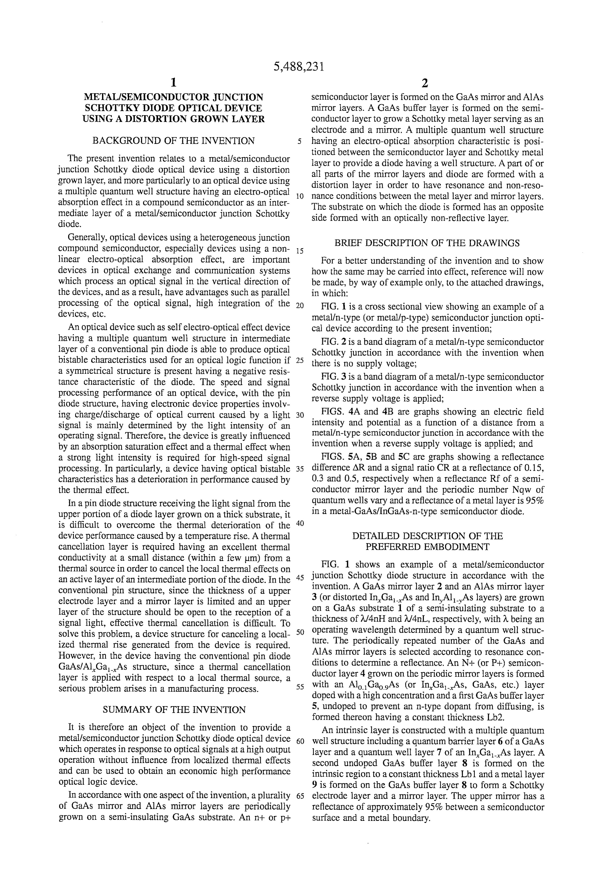
METAL/SEMICONDUCTOR JUNCTION semiconductor layer is formed on the GaAs mirror and AlAs SCHOTTKY DODE OPTICAL DEVICE mirror layers. A GaAs buffer layer is formed on the semi USING A DISTORTION GROWN LAYER conductor layer to grow a Schottky metal layer Serving as an electrode and a mirror. A multiple quantum well structure
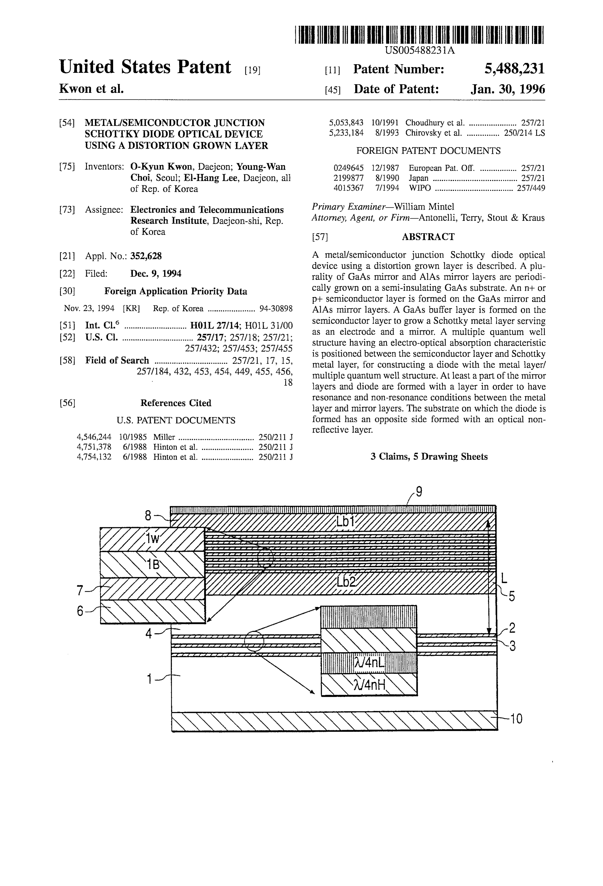
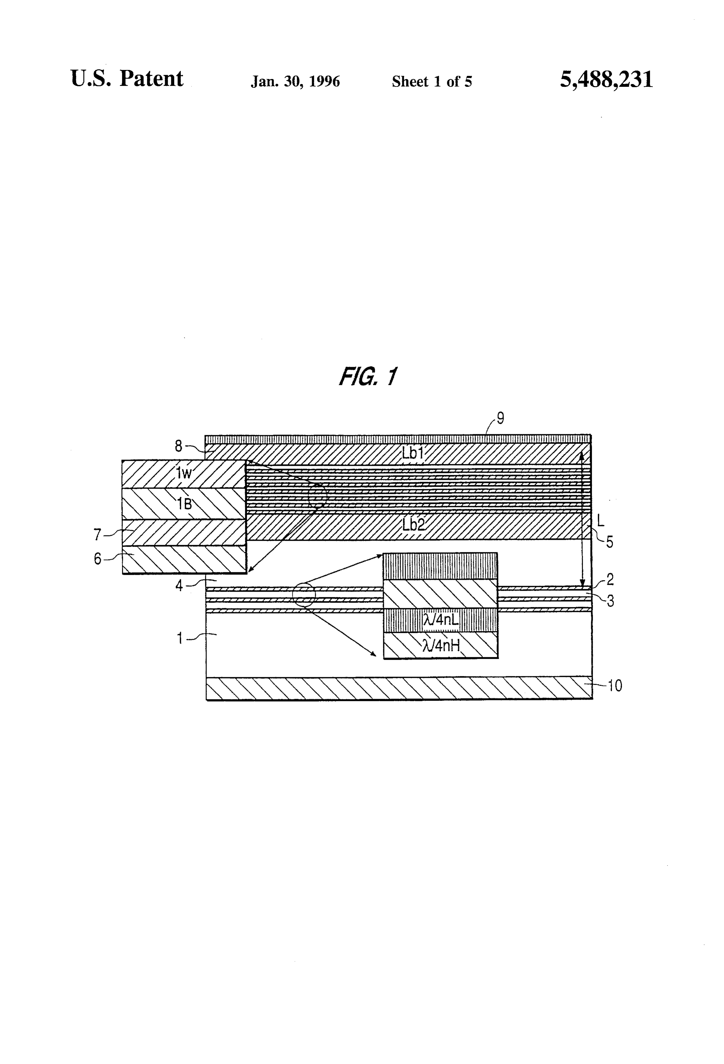
BACKGROUND OF THE INVENTION having an electro-optical absorption characteristic is posi The present invention relates to a metal/semiconductor tioned between the semiconductor layer and Schottky metal junction Schottky diode optical device using a distortion layer to provide a diode having a well structure. A part of or grown layer, and more particularly to an optical device using all parts of the mirror layers and diode are formed with a distortion layer in order to have resonance and non-reso a multiple quantum well structure having an electro-optical 10 nance conditions absorption effect in a compound semiconductor as an inter between the metal layer and mirror layers. mediate layer of a metal/semiconductor junction Schottky The substrate on which the diode is formed has an opposite diode. side formed with an optically non-reflective layer. Generally, optical devices using a heterogeneous junction BRIEF DESCRIPTION OF THE DRAWINGS compound semiconductor, especially devices using a non 15 linear electro-optical absorption effect, are important For a better understanding of the invention and to show devices in optical exchange and communication systems how the same may be carried into effect, reference will now which process an optical signal in the vertical direction of be made, by way of example only, to the attached drawings, the devices, and as a result, have advantages such as parallel in which:
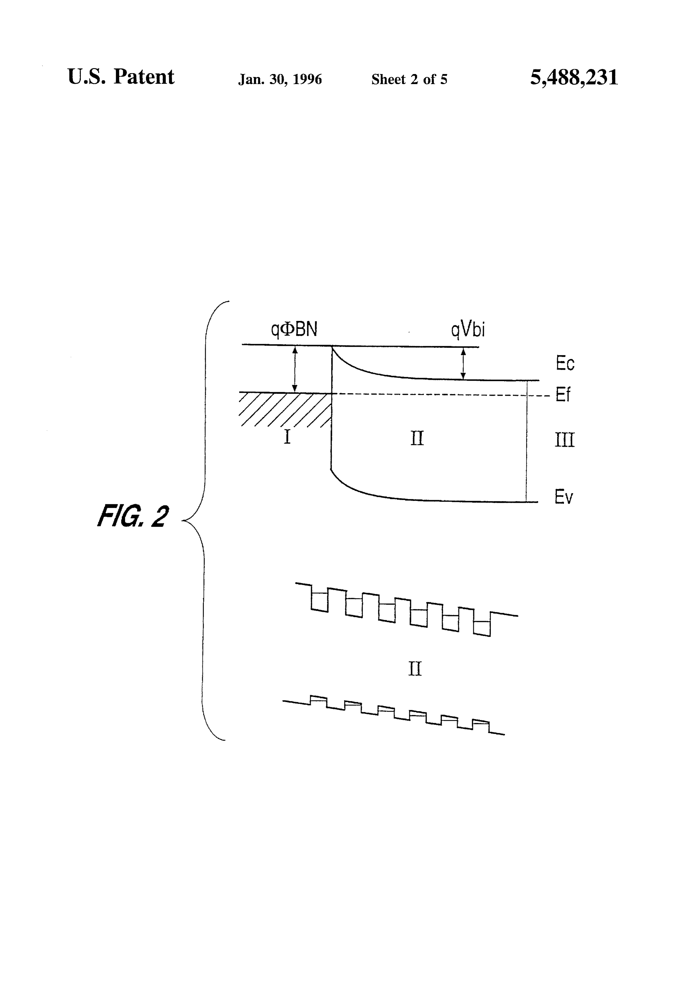
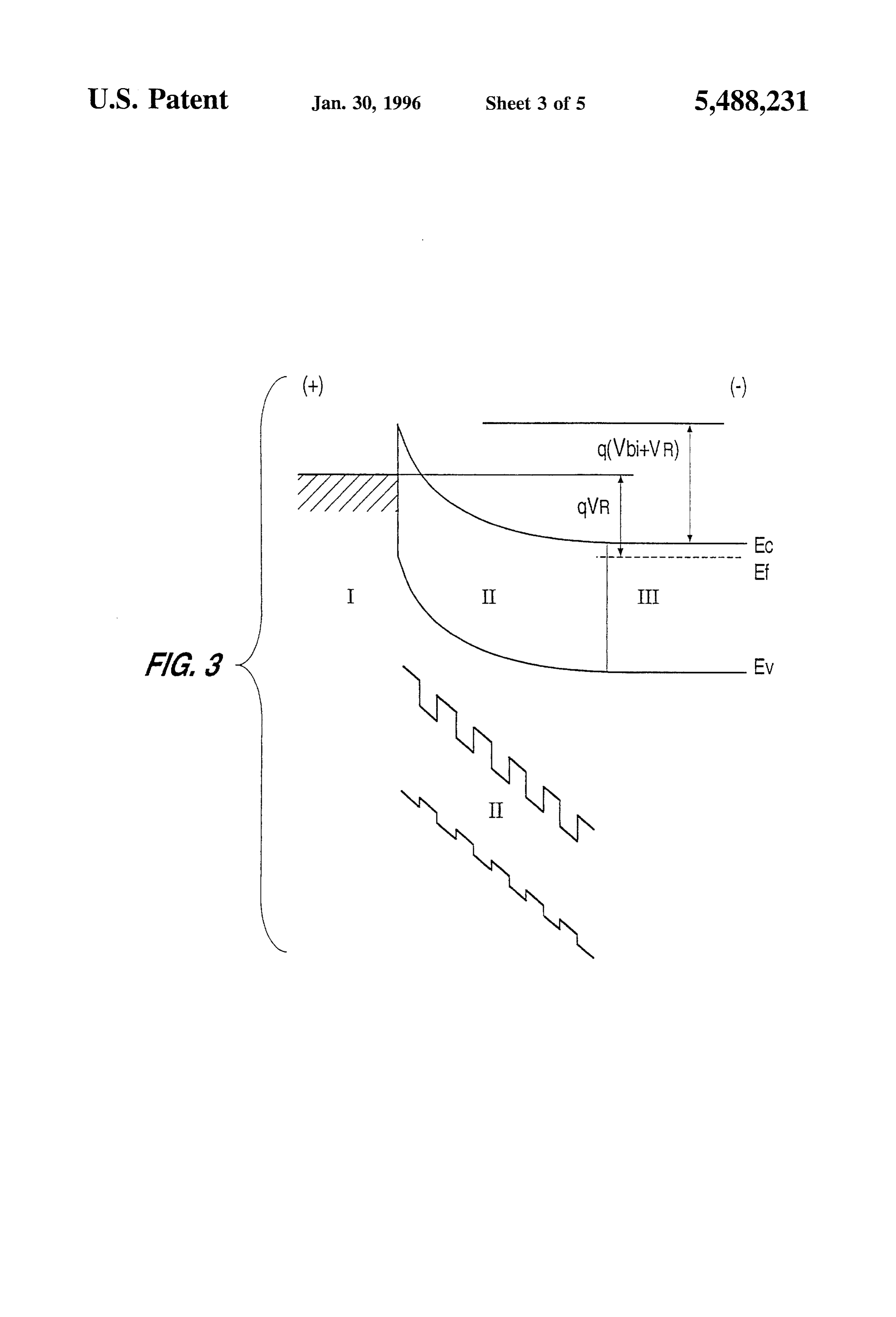
processing of the optical signal, high integration of the 20 FIG. 1 is a cross sectional view showing an example of a devices, etc. metal/n-type (or metal/p-type) semiconductor junction opti An optical device such as self electro-optical effect device cal device according to the present invention; having a multiple quantum well structure in intermediate FIG. 2 is a band diagram of a metal/n-type semiconductor layer of a conventional pin diode is able to produce optical Schottky junction in accordance with the invention when bistable characteristics used for an optical logic function if 25 there is no supply voltage;
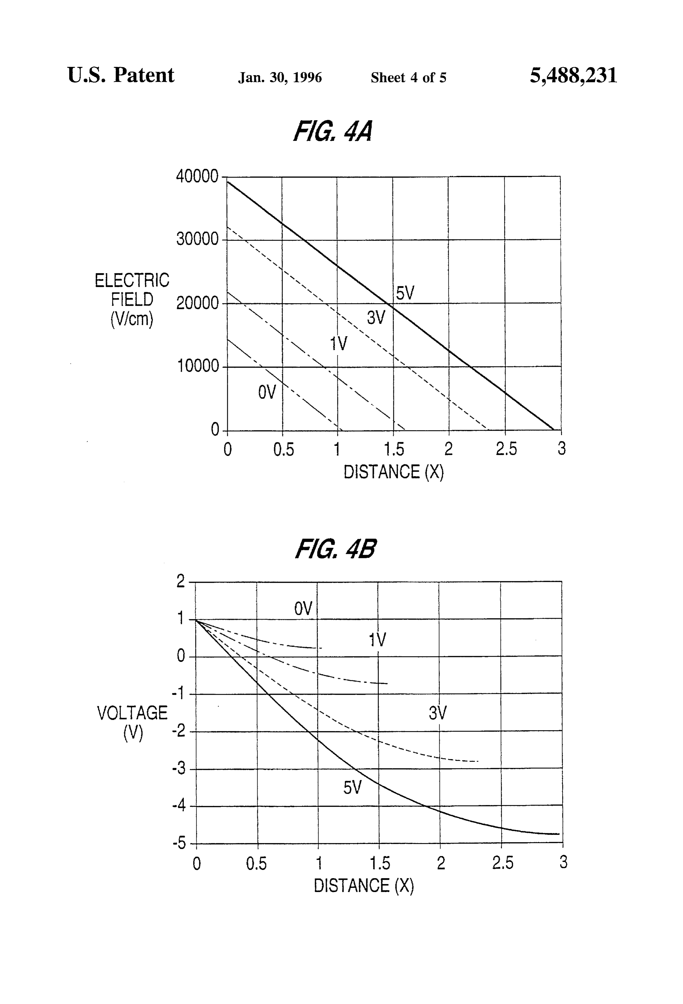
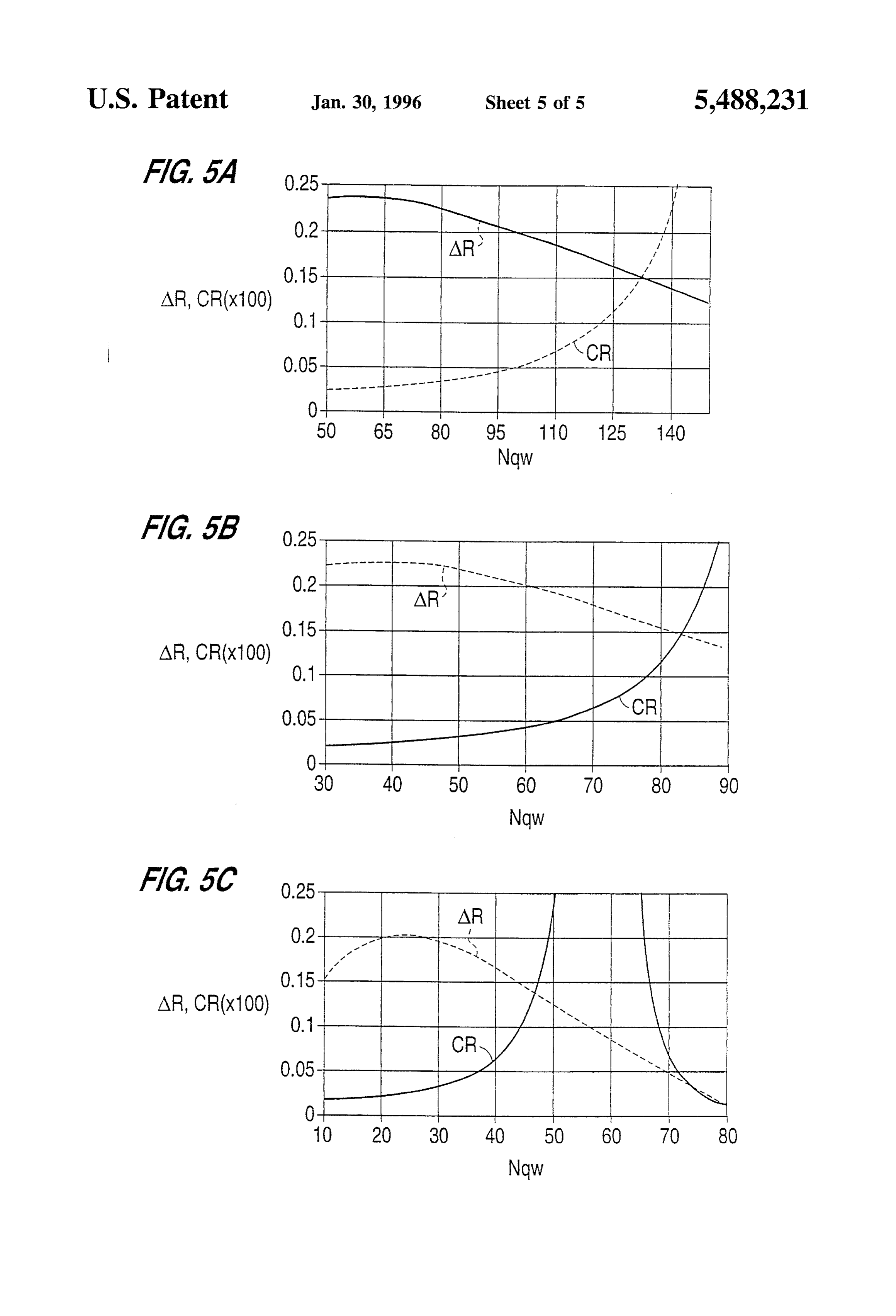
a symmetrical structure is present having a negative resis FIG.3 is aband diagram of a metal/n-type semiconductor tance characteristic of the diode. The speed and signal Schottky junction in accordance with the invention when a processing performance of an optical device, with the pin reverse supply voltage is applied; diode structure, having electronic device properties involv ing charge/discharge of optical current caused by a light 30 FIGS. 4A and 4B are graphs showing an electric field signal is mainly determined by the light intensity of an intensity and potential as a function of a distance from a operating signal. Therefore, the device is greatly influenced metal/n-type semiconductor junction in accordance with the by an absorption saturation effect and a thermal effect when invention when a reverse supply voltage is applied; and a strong light intensity is required for high-speed signal FIGS.5A, 5B and 5C are graphs showing a reflectance processing. In particularly, a device having optical bistable 35 difference AR and a signal ratio CR at a reflectance of 0.15, characteristics has a deterioration in performance caused by 0.3 and 0.5, respectively when a reflectance Rf of a semi the thernal effect. conductor mirror layer and the periodic number Naw of In a pin diode structure receiving the light signal from the quantum wells vary and a reflectance of a metal layer is 95% upper portion of a diode layer grown on a thick substrate, it in a metal-GaAs/InGaAs-n-type semiconductor diode. is difficult to overcome the thermal deterioration of the 40 device performance caused by a temperature rise. A thermal DETAILED DESCRIPTION OF THE cancellation layer is required having an excellent thermal PREFERRED EMBODIMENT conductivity at a small distance (within a few um) from a thermal source in order to cancel the local thermal effects on FIG. 1 shows an example of a metal/semiconductor an active layer of an intermediate portion of the diode. In the 45 junction Schottky diode structure in accordance with the conventional pin structure, since the thickness of a upper invention. A GaAs mirror layer 2 and an AlAs mirror layer electrode layer and a mirror layer is limited and an upper 3 (or distorted InGaAs and In, Al-As layers) are grown layer of the structure should be open to the reception of a on a GaAs substrate 1 of a semi-insulating substrate to a signal light, effective thermal cancellation is difficult. To 50 operating of thickness W4nH and W4nL, respectively, with W being an wavelength determined by a quantum well struc solve this problem, a device structure for canceling a local ture. The periodically repeated number of the GaAs and ized thermal rise generated from the device is required.
However, in the device having the conventional pin diode AlAs mirror layers is selected according to resonance con GaAs/AlGaAs structure, since a thermal cancellation ditions to determine a reflectance. An N-t- (or P-H) semicon ductor layer 4 grown on the periodic mirror layers is formed layer is applied with respect to a local thermal source, a serious problem arises in a manufacturing process. 55 with an Alo, Gao oAS (or InGaAs, GaAs, etc.) layer doped with a high concentration and a first GaAs buffer layer
SUMMARY OF THE INVENTION 5, undoped to prevent an n-type dopant from diffusing, is formed thereon having a constant thickness Lb2.
It is therefore an object of the invention to provide a An intrinsic layer is constructed with a multiple quantum metal/semiconductor junction Schottky diode optical device 60 well structure including a quantum barrier layer 6 of a GaAs which operates in response to optical signals at a high output layer and a quantum well layer 7 of an InGaAs layer. A operation without influence from localized thermal effects second undoped GaAs buffer layer 8 is formed on the and can be used to obtain an economic high performance intrinsic region to a constant thickness Lb1 and a metal layer optical logic device. 9 is formed on the GaAs buffer layer 8 to form a Schottky In accordance with one aspect of the invention, a plurality 65 electrode layer and a mirror layer. The upper mirror has a of GaAs mirror and AlAs mirror layers are periodically reflectance of approximately 95% between a semiconductor grown on a semi-insulating GaAs substrate. An n- or p surface and a metal boundary.
Page 8
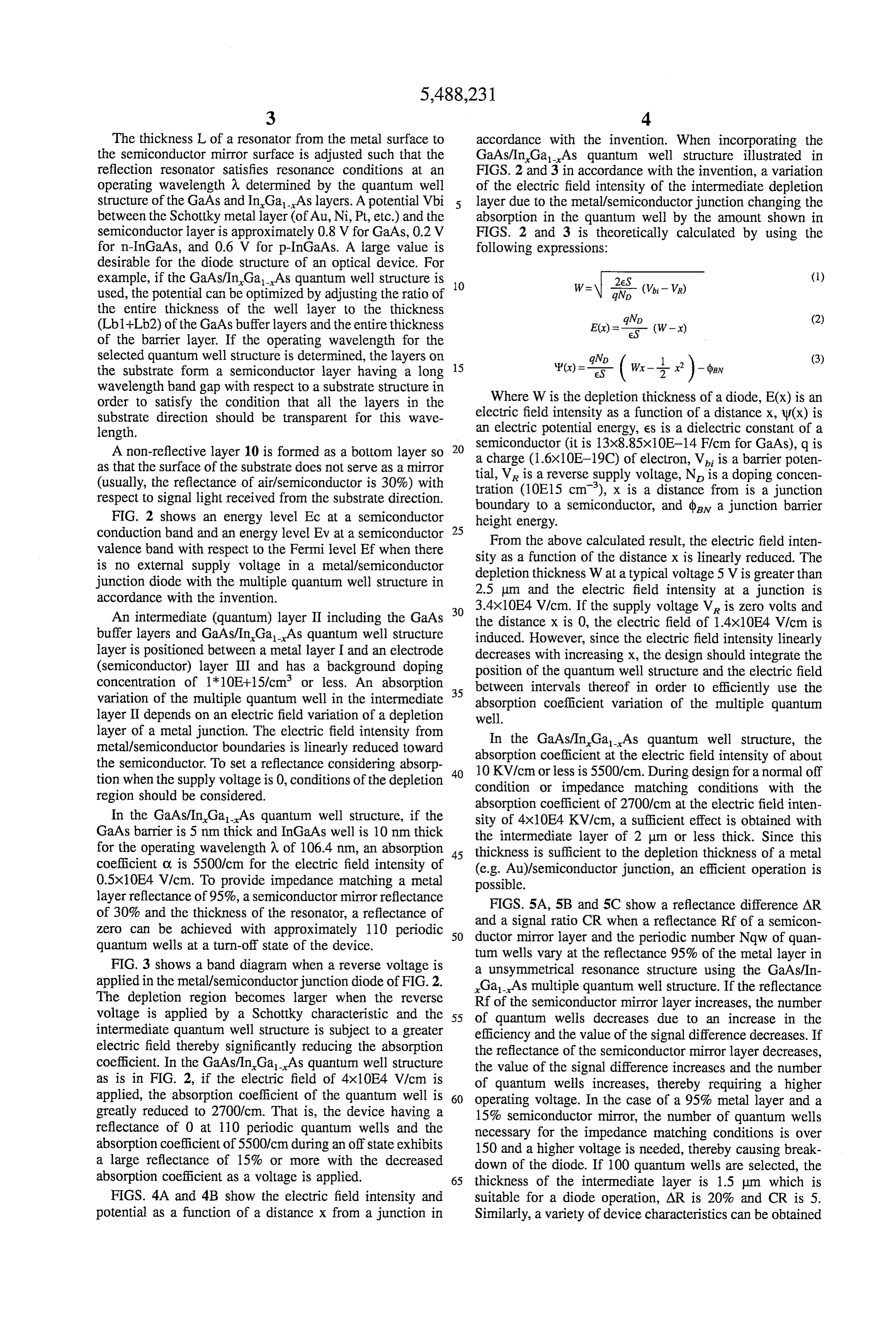
The thickness L of a resonator from the metal surface to accordance with the invention. When incorporating the the semiconductor mirror surface is adjusted such that the GaAs/InGaAs quantum well structure illustrated in reflection resonator satisfies resonance conditions at an FIGS. 2 and 3 in accordance with the invention, a variation operating wavelength determined by the quantum well of the electric field intensity of the intermediate depletion structure of the GaAs and InGaAs layers. A potential Vbi layer due to the metal/semiconductor junction changing the between the Schottky metal layer (of Au, Ni, Pt, etc.) and the absorption in the quantum well by the amount shown in semiconductor layer is approximately 0.8 V for GaAs, 0.2V FIGS. 2 and 3 is theoretically calculated by using the for n-InCaAs, and 0.6 V for p-InGaAs. A large value is following expressions:
desirable for the diode structure of an optical device. For example, if the GaAs/InGaAs quantum well structure is 10 (1) used, the potential can be optimized by adjusting the ratio of the entire thickness of the well layer to the thickness (2) (Lb1+Lb2) of the GaAs buffer layers and the entire thickness of the barrier layer. If the operating wavelength for the selected quantum well structure is determined, the layers on (3) the substrate form a semiconductor layer having a long 15 wavelength band gap with respect to a substrate structure in order to satisfy the condition that all the layers in the Where W is the depletion thickness of a diode, E(x) is an substrate direction should be transparent for this wave electric field intensity as a function of a distance x, y(x) is length. an electric potential energy, es is a dielectric constant of a A non-reflective layer 10 is formed as a bottom layer so 20 semiconductor (it is 13x8.85x10E-14 F/cm for GaAs), q is as that the surface of the substrate does not serve as a mirror a charge (1.6x10E-19C) of electron, V is a barrier poten (usually, the reflectance of air/semiconductor is 30%) with tial, V is a reverse supply voltage, N is a doping concen respect to signal light received from the substrate direction. tration (10E15 cm), x is a distance from is a junction boundary to a semiconductor, and (by a junction barrier
FIG. 2 shows an energy level Ec at a semiconductor height energy.
conduction band and an energy level Ev at a semiconductor 25 From the above calculated result, the electric field inten valence band with respect to the Fermi level Ef when there sity as a function of the distance x is linearly reduced. The is no external supply voltage in a metal/semiconductor depletion thickness Wata typical voltage 5V is greater than junction diode with the multiple quantum well structure in 2.5 um and the electric field intensity at a junction is accordance with the invention.
3.4x10E4 V/cm. If the supply voltage V is zero volts and
An intermediate (quantum) layer II including the GaAs 30 the distance x is 0, the electric field of 1.4x10E4 V/cm is buffer layers and GaAs/InGaAs quantum well structure induced. However, since the electric field intensity linearly layer is positioned between a metal layer I and an electrode decreases with increasing X, the design should integrate the (semiconductor) layer III and has a background doping position of the quantum well structure and the electric field concentration of 1*10E-15/cm or less. An absorption 35 between intervals thereof in order to efficiently use the variation of the multiple quantum well in the intermediate absorption coefficient variation of the multiple quantum layer II depends on an electric field variation of a depletion well.
layer of a metal junction. The electric field intensity from In the GaAs/InGaAs quantum well structure, the metal/semiconductor boundaries is linearly reduced toward the semiconductor. To set a reflectance considering absorp 40 absorption
coefficient at the electric field intensity of about or less is 5500/cm. During design for a normal off tion when the supply voltage is 0, conditions of the depletion condition or impedance matching conditions with the region should be considered. absorption coefficient of 2700/cm at the electric field inten In the GaAs/InGaAs quantum well structure, if the sity of 4x10E4 KV/cm, a sufficient effect is obtained with GaAs barrier is 5 nm thick and InGaAs well is 10 nm thick the intermediate layer of 2 um or less thick. Since this for the operating wavelength W of 106.4 nm, an absorption 45 thickness is sufficient to the depletion thickness of a metal coefficient o is 5500/cm for the electric field intensity of (e.g. Au)/semiconductor junction, an efficient operation is 0.5x10E4 V/cm. To provide impedance matching a metal possible.
layer reflectance of 95%, a semiconductor mirror reflectance FIGS.5A, 5B and 5C show a reflectance difference AR of 30% and the thickness of the resonator, a reflectance of and a signal ratio CR when a reflectance Rf of a semicon zero can be achieved with approximately 110 periodic 50 ductor mirror layer and the periodic number Now of quan quantum wells at a turn-off state of the device. tum wells vary at the reflectance 95% of the metal layer in FIG. 3 shows a band diagram when a reverse voltage is a unsymmetrical resonance structure using the GaAs/In applied in the metal/semiconductorjunction diode of FIG.2. GaAs multiple quantum well structure. If the reflectance The depletion region becomes larger when the reverse voltage is applied by a Schottky characteristic and the 55 of of Rf the semiconductor mirror layer increases, the number quantum wells decreases due to an increase in the intermediate quantum well structure is subject to a greater efficiency and the value of the signal difference decreases. If electric field thereby significantly reducing the absorption the reflectance of the semiconductor mirror layer decreases, coefficient. In the GaAs/InGaAs quantum well structure the value of the signal difference increases and the number as is in FIG. 2, if the electric field of 4x10E4 V/cm is of quantum wells increases, thereby requiring a higher applied, the absorption coefficient of the quantum well is 60 operating voltage. In the case of a 95% metal layer and a greatly reduced to 2700/cm. That is, the device having a 15% semiconductor mirror, the number of quantum wells reflectance of 0 at 110 periodic quantum wells and the necessary for the impedance matching conditions is over absorption coefficient of 5500/cm during an off state exhibits 150 and a higher voltage is needed, thereby causing break a large reflectance of 15% or more with the decreased down of the diode. If 100 quantum wells are selected, the absorption coefficient as a voltage is applied. 65 thickness of the intermediate layer is 1.5 um which is FIGS. 4A and 4B show the electric field intensity and suitable for a diode operation, AR is 20% and CR is 5. potential as a function of a distance X from a junction in Similarly, a variety of device characteristics can be obtained
Page 9
by adjusting the reflectance difference AR, signal ratio CR, 5) The deterioration of device performance caused by a operating voltage, reflectance of the semiconductor mirror, local temperature rise is overcome by forming a junction etc., with these values being maintained at operating light by between the metal layer and the intermediate layer of the a thermal conduction effect of the metal layer. Therefore, Schottky diode.
applications with laser light etc. for a high-speed operation While there is shown and described the preferred embodi is possible.
As described above, the optical logic device using the ment of invention, it will be understood by those skilled in metal/n-type (or p-type) semiconductor junction Schottky the art that foregoing and other changes in form and details diode according to the present invention has the following may be made without departing from the spirit and scope of characteristics: 10 the present invention.
What is claimed is:
1) The thin doping intermediate layer and the metal layer 1. A metal/semiconductor junction Schottky diode optical forming a Schottky junction are applied instead of a p-type device formed on a structure comprising: (or n-type) electrode layer and a upper mirror layer of the conventional pin structure. The upper metal layer is used as 15 a plurality of GaAs mirror and AlAs mirror layers grown a mirror with a high reflectance and semiconductor mirror on a semi-insulating GaAs substrate, one of an n+ and layers corresponding to the bottom mirror of the conven a p+ semiconductor layer formed on said GaAs mirror tional pin structure is used as a mirror with a low reflectance. and AlAs mirror layers, a GaAs buffer layer formed on The bottom of the GaAs substrate is formed with a non said one of said n+ and p-- semiconductor layer pro reflective layer and thus an optical signal is received from 20 viding a Schottky metal layer serving as an electrode the substrate direction. and a mirror, and a multiple quantum well structure 2) To achieve an optical logic device structure receiving having an electro-optical absorption characteristic, the optical signal from the substrate direction, the multiple formed between said one of said n+ and p-- semicon quantum well structure using a compound semiconductor ductor layer and Schottky metal layer, to provide a with a wavelength region longer than GaAs is formed with 25 diode with said multiple quantum well structure. a distortion grown layer and the position within the inter 2. A metal/semiconductor junction Schottky diode optical mediate layer is optimized. device as claimed in claim 1, wherein at least a part of said 3) The optical logic structure and optical modulation mirror layers and diode are formed with a layer in order to structure can be achieved by optimizing the periodic number have resonance and non-resonance conditions between said of quantum wells and the position within the intermediate 30 metal layer and mirror layers.
layer. 3. A metal/semiconductor junction Schottky diode optical 4) Growth steps are simplified by omitting a growth device as claimed in claim 1, wherein said substrate on process of the p-type (or n-type) semiconductor and the which said diode is formed has an opposite side formed with upper mirror layer of the conventional optical device struc an optical non-reflective layer. ture. Since the device manufacturing process is reduced, there are economic advantages. cic k sk ck ck
Provenance
- Collection
- Cited prior art
- Original PDF
- patentimages.storage.googleapis.com →
- Filed
- 1994-12-09
- Pages
- 9
- Method
- pdftotext (the PDF's own text layer) + pdftoppm 300dpi page scans
- Source
- Google Patents bibliographic record
- Granted
- 1996-01-30
- Inventors
- O-Kyun Kwon; Young-Wan Choi; El-Hang Lee; Electronics and Telecommunications Research Institute ETRI
- Transcribed from
- patentimages.storage.googleapis.com →