patent · US6344272
Metal nanoshells
5 February 2002
Page 1 — bibliographic record
(12) United States Patent (10) Patent No.: US 6,344,272 B1 Oldenburg et al. (45) Date of Patent: *Feb. 5, 2002
(54) METAL NANOSHELLS FOREIGN PATENT DOCUMENTS (75) Inventors: Steven J. Oldenburg; Richard D. WO WO901 1890 10/1990 Averitt; Nancy J. Halas, all of OTHER PUBLICATIONS
Houston, TX (US)
Birnboim, Meyer H., “Nonlinear Optical Properties of (73) Assignee: Wm. Marsh Rice University, Houston, Structured Nanoparticle Composites”, Mat. Res. Soc. Symp. TX (US) Proc. vol. 164, 1990, pp. 277–282.
(*) Notice: This patent issued on a continued pros- Nedelijkovic, Jovan, “Observation
ecution application filed under 37 CFR Optical Extinction in Silver-Coated Silver Bromide Nano particles”,22 American Institute of Physics, Jun. 3, 1991, pp.
1.53(d), and is subject to the twenty year 2461-2463 patent term provisions of 35 U.S.C. 66 ss 154(a)(2). Oldenburg, S.J., “Nanoengineering of Optical Resonances',
Subject to any disclaimer, the term of this Westcott, Sarah, “Formation and Adsorption of Clusters of patent is extended or adjusted under 35 Gold Nanoparticles onto Functionalized Silica Nanoparticle U.S.C. 154(b) by 0 days. Surfaces”, Langmuir, 1998, vol. 14, No. 19, pp. 5396-5401.
(List continued on next page.)
(22) Filed: Mar 11, 1998 Primary Examiner William Krynski Assistant Examiner B. Shewareged
Related U.S. Application Data (74) Attorney, Agent, or Firm-Conley, Rose & Tayon, PC (60) Provisional application No. 60/040,971, filed on Mar. 12, 1997, and provisional application No. 60/040,570, filed on (57) ABSTRACT
7 The present invention is for particulate compositions and (51) Int. Cl." ................................................ B32B 15/02 methods for producing them that can absorb or Scatter (52) U.S. Cl. ....................... 428/403; 428/404; 428/913; electromagnetic radiation. The particles are homogeneous in 252/587 Size and are comprised of a nonconducting inner layer that (58) Field of Search ................................. 428/403, 404, is Surrounded by an electrically conducting material. The 428/913; 252/478, 518, 520, 587 ratio of the thickness of the nonconducting layer to the thickness of the outer conducting shell is determinative of (56) References Cited the wavelength of maximum absorbance or Scattering of the
particle. Unique Solution phase methods for Synthesizing the particles involve linking clusters of the conducting atoms, 3.856,398 A 12/1974 Taylor ......................... 355/63 ions, or molecules to the nonconducting inner layer by linear 4,099,854 A 7/1978 Decker et al. ....... ... 350/312 molecules. This step can be followed by growth of the metal 4,123,396 A 10/1978 Rembaum et al. ............ 326/24 onto the clusters to form a coherent conducting shell that 4,313,734. A 2/1982 Leuvering ................. 23/230B encapsulates the core.
4,416.998 A 11/1983 Adams et al. ................ 436/86
(List continued on next page.) 49 Claims, 3 Drawing Sheets
500 600 700 800 900 1OOO 1100 1200
Wavelength (nm)
Increasing
Core: Shell Ratio
Page 2
4,452,773 A 6/1984 Molday ...................... 424/1.1 particles; Web Publication; Jan. 10, 1997; (1 p.). 4,481,091 A 11/1984 Brus et al. . ... 204/157.1 R J. I. Steinfeld; An Introduction to Modern Molecular Spec 4,624,923 A 11/1986 Margel ....................... 435/176 troscopy; The MIT Press; Second Edition: CopyrightC)1974 4,877,647 A 10/1989 Klabunde ..... ... 427/123 and 1985; (8 p.).
4,979,821 A 12/1990 Schutt et al. ..... ... 356/246 5,023,139 A * 6/1991 Birnboim et al. ........... 428/402 P. F. Bernath; Spectra of Atoms and Molecules; Oxford 5,025,147 A 6/1991 Durig et al. ................ 250/216 University Press 1995; (8 p.).
5,213,895 A 5/1993 Hirai et al. .... ... 428/403 5,249,077 A 9/1993 Laronga et al. ... 359/385 R. D. Averitt, et al; Ultrafast Electron Dynamics in Gold 5,322,798 A 6/1994 Sadowski ......... ... 436/113 NanoShells; The American Physical Society vol. 58, No. 16; 5,338,353 A 8/1994 Uchino et al. .............. 106/426 1998; (4 p.).
5,376,556 A 12/1994 Tarcha et al. ............... 436/525 J. W. Haus, et al; Nonlinear-Optical Properties of Conduc 5,451,525 A 9/1995 Shenkin et al. ............... 436/63 tive Spheroidal Particle Composites; Optical Society of 5,479,024 A 12/1995 Hillner et al. .... 250/458.1 5,501,949 A 3/1996 Marshall ........................ 435/5 America, vol. 6, No. 4, Apr. 1989; (pp. 797-807). 5,521,289 A 5/1996 Hainfeld et al. ......... 530/391.5 D. Stroud, et al; Decoupling Approximation for the Nonlin 5,545,250 A * 8/1996 Bergmann et al. ............ 75/252 ear-Optical Response of Composite Media; Optical Society 5,552,086 A 9/1996 Siiman et al. .... 252/408.1 5,567,628 A 10/1996 Tarcha et al. ..... ... 436/525 of America, vol. 6, No. 4, Apr. Apr. 1989; (pp. 778-786). 5,599,668 A 2/1997 Stimpson et al. .............. 435/6 A. E. Neeves, et al; Composite Structures for the Enhance 5,817.462 A 10/1998 Garini et al. .................. 435/6 ment of Nonlinear-Optical Susceptibility; Optical Society of 5,845,083 A * 12/1998 Hamadani et al. ..... 395/200.61 America; vol. 6, No. 4, Apr. 1989; (pp. 787-796). 5,938,617 A 8/1999 Vo-Dinh ..................... 600/476 6,180,415 B1 1/2001 Svhultz et al. .............. 436/518 P. Barnickel, et al; Silver Coated Latex Spheres; Molecular OTHER PUBLICATIONS Physics, 1989, vol. 67, No. 6; (pp. 1355–1372). Zhou, H.S., “Controlled Synthesis and Quantum-Size Effect R. D. Averitt, et al; Plasmon Resonance Shifts of Au-Coated in Gold-Coated Nanoparticles”, American Physical Society, AuS NanoShells. Insight into Multicomponent Nanoparticle 1994, vol. 50, No. 16, pp. 12 052–12 056. Growth; Physical Review Letters, Jun. 2, 1997, vol. 78, No. Zhou, H.S., “Synthesis and Optical Properties of Coated 22, (pp. 4217-4220).
Nanoparticle Composites”, Jornal of Luminescence, 70, D. Sarkar, et al; General Vector Basis Function Solution of 1996, pp. 21-34. Maxwell's Equations; Physical Review, vol. 56, No. 1 Jul. R. D. Averitt, et al;Optical Properties and Growth Kinetics 1997; (pp. 1102-1112).
of Au coted au 2S NanoShells; Web Publication ; Jan. 10, 1997; (1 p.). * cited by examiner

Page 3
Drawing sheet — no readable text.
Page 4
Drawing sheet — no readable text.
Page 5
Drawing sheet — no readable text.
Page 6
METAL NANOSHELLS sodium sulfide) particles has been shown to red shift the gold colloid absorption maximum from 520 nm to between
CROSS-REFERENCE TO RELATED approximately 600 nm and 900 nm, depending on the APPLICATIONS amount of gold deposited on the AuS core and the size of This application relies for priority on the following two the core. Zhou, et al. (1994). The ratio of the core radius to provisional applications: the first application is entitled shell thickneSS can be controlled by changing the reactant Metal Nanoshells and is to Oldenburg et al., and was filed diameter of the orparticle concentrations, by Stopping the reaction. In this case, the core is directly proportional to the
application is entitled Metal Nanoshells is to Oldenburg et plasmon resonance. However, ofgold-Sulfide red shift in the wavelength light that induces gold particle diam al., and was filed on Mar. 14, 1997 and the Ser. No. of that eters are limited to sizes of approximately 40-45 nm with a application is 60/040,570. These applications are specifi thin gold shell (less than 5 nm). The limited size of the cally included herein by reference. gold-Sulfide particles of Zhou et al. limits the absorbance STATEMENT REGARDING FEDERALLY maximum to wavelengths no larger than 900 nm. See, also
SPONSORED RESEARCH OR DEVELOPMENT
An additional limitation of Such particles as defined by
The research that resulted in this invention was funded by Zhou et al. is that both the core and the shell are grown as the Office of Naval Research, NO0014-97-1-0217, and the a result of a Single chemical reaction, thus limiting the National Science Foundation, ECS-9258118. choice of the core material and the shell material to AuS
BACKGROUND OF THE INVENTION
and Au respectively. In addition, only the ratio of the core radius to Shell thickness may be controlled; independent
It is known that Solid metal nanoparticles (i.e. Solid, Single control of the core radius and the Shell thickness is not metal spheres of uniform composition and nanometer possible.
dimensions) possess unique optical properties. In particular, 25 Neideljkovic and Patel (1991) disclosed silver-coated metal nanoparticles (especially the coinage metals) display silver bromide particles that are produced by intense UV a pronounced optical resonance. This So-called plasmon irradiation of a mixture of Silver bromide, Silver, Sodium resonance is due to the collective coupling of the conduction dodecylsulfate (SDS) and ethylenediamine tetraacetic acid electrons in the metal sphere to the incident electromagnetic (EDTA). The Neideljkovic particles range in size from field. This resonance can be dominated by absorption or approximately 10 to 40 nm and are irregularly-shaped, as Scattering depending on the radius of the nanoparticle with determined by transmission electron micrography. respect to the wavelength of the incident electromagnetic Predictably, the Spectra obtained from these particle prepa radiation. ASSociated with this plasmon resonance is a Strong rations are extremely broad.
local field enhancement in the interior of the metal nano In U.S. Pat. No. 5,023,139, Birnboim et al. disclosed particle. A variety of potentially useful devices can be 35 theoretical calculations indicating that metal-coated, Semi fabricated to take advantage of these Specific optical prop conducting, nanometer-sized particles containing should erties. For example, optical filters or chemical Sensors based exhibit third-order nonlinear optical susceptibility relative to on Surface enhanced Raman Scattering (SERS) have been uncoated dielectric nanoparticles (due to local field fabricated. enhancement). Their static calculations were based on hypo A Serious practical limitation to realizing many applica 40 thetical compositions. The preferred embodiments disclosed tions of Solid metal nanoparticles is the inability to position by Birnboim et al. are, in fact, not particles with metallic the plasmon resonance at technologically important wave shells on their surfaces. In those embodiments theoretically lengths. For example, Solid gold nanoparticles of 10 nm in proposed by Birnboim et al. that do in fact propose a metal diameter have a plasmon resonance centered at 520 nm. This outer shell, there is an additional requirement as to the plasmon resonance cannot be controllably shifted by more 45 Specific medium in which they must be used in order to than approximately 30 nanometers by varying the particle properly function.
diameter or the Specific embedding medium. However, Birnboim does not disclose methods for pre Metal colloids have a variety of useful optical properties paring the disclosed hypothetical compositions. including a strong optical absorption and an extremely large Furthermore, Birnboim's calculations do not take into and fast third-order nonlinear optical (NLO) polarizability. 50 account Surface electron Scattering. Surface electron Scat These optical properties are attributed to the phasic response tering Strongly modifies the optical response of all metallic of electrons in the metallic particles to electromagnetic Structures that possess at least one dimension Smaller than fields. This collective electron excitation is known as plas the bulk electron mean free path (e.g. in Au at room O CSOCC. temperature the bulk electron mean free path is about 40 At resonance, dilute metal colloid Solutions have the 55 nm). This effect reduces the local field enhancement factor largest electronic NLOSusceptibility of known Substances. that in turn reduces the resonant third order nonlinear optical However, the utility of these solutions is limited because Susceptibility associated with the nanoshell geometry. See, their plasmon resonance is confined to relatively narrow Averitt et al. (1997). Since typical shell thicknesses for these wavelength ranges and cannot readily be shifted. For compositions fall below 40 nm, Birnboim et al’s theoretical example, Silver particles 10 nm in diameter absorb light 60 calculations fail to account for this effect which is an maximally at approximately 355 nm, while Similar sized important aspect of the optical response for functional metal gold particles absorb maximally at about 520 nm. These nanoshells. Finally, it is important to realize that the hypo absorbance maximums are insensitive to changes in particle thetical metal nanoshells of Birnboim pertains Specifically to Size and various dielectric coatings on the particles. the enhancement of the third order nonlinear optical Sus One method of overcoming this problem is to coat Small 65 ceptibility.
nonconducting particles with these metals. For example, the Moreover, Birnboim-type particles are by definition par reduction of Au on AuS (reduction of chloroauric acid with ticles much Smaller than a wavelength of light (less than
Page 7
0.10 times a given wavelength of light), and are particles in The Spectral location of the maximum of the plasmon which the dielectric property of the nanoshell (in those resonance peak for this geometry depends Sensitively upon instances where it is in fact a metal shell that is used in the ratio of the core radius to Shell thickness, as well as the Birnboim et al.) are defined as the bulk dielectric property of dielectric functions of the core and shell. The presence of a the metal Selected. In practice, this requires these Smaller dielectric core shifts the plasmon resonance to longer wave than-a-wavelength particles to have metal Shell layer thick lengths relative to a Solid nanoparticle made exclusively of nesses of many nanometers (e.g., for Au, Such minute the metallic shell material. For a given core radius, a thin particles meeting the theoretical requirements of the Birn shell will have a plasmon peak that is shifted to longer boim calculations and the bulk dielectric properties of Au wavelengths that metal relative to a thicker shell. It is to be emphasized nanoshells possess all of the same technologically required thereby, would necessarily have shells at least 40 viable optical properties nm in thickness). The physical limitations placed on the addition to this extremelyasimportant Solid metal nanoparticles in aspect of resonance construction of Such particles is therefore considerable. tunability.
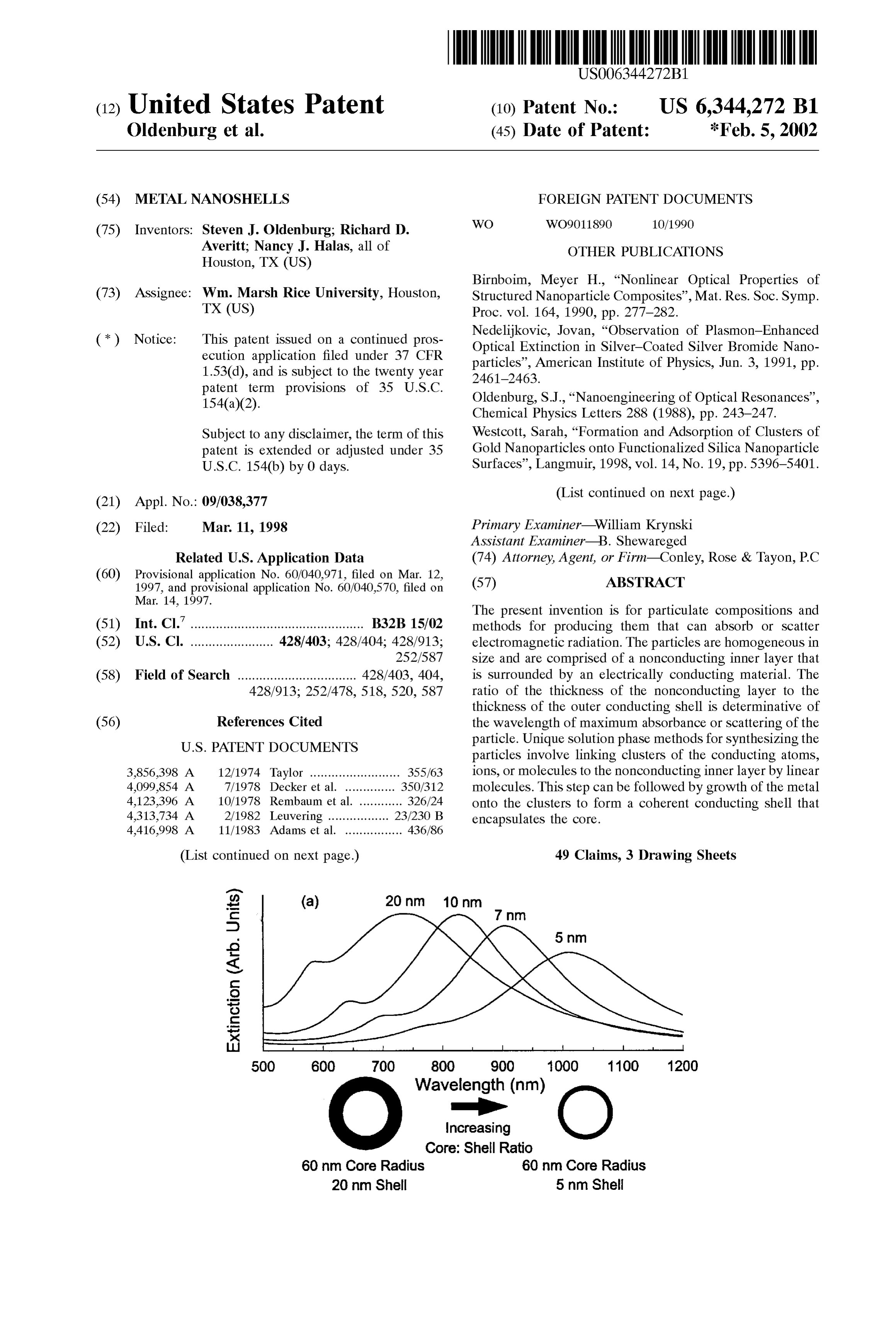
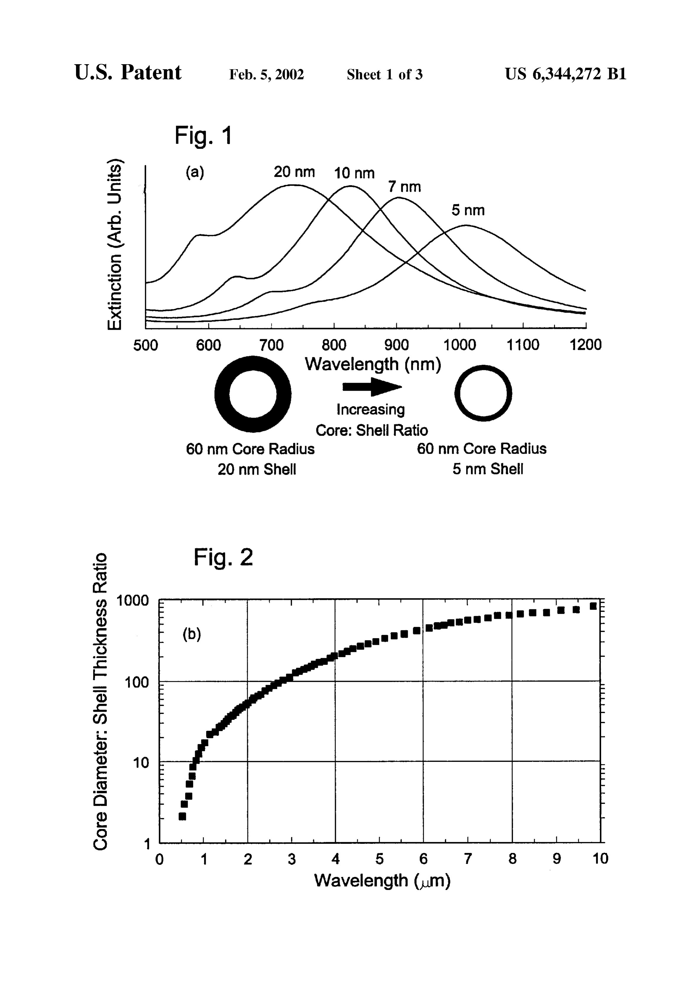
Methods and materials are needed that can be used to shift the wavelength of maximum absorption of metal colloids. method This invention relates in certain regards to a general Methods for producing materials having defined wavelength particular,forthethe 15 production of nanoshell composites. In absorbance maxima acroSS the Visible and infrared range of be determined choice of the core material and geometry can independently of the shell material. Similarly, the electromagnetic Spectrum are needed. Particularly, Such the choice of the shell material and shell thickness is metal nanoshell composites should be constructed in a independent of the desired core material. It is also important manner to allow a choice of core material, core dimensions, and core geometry independent of those criteria for the shell to note that the coating methods and materials described material. Compositions produced by these methods should herein will allow for the fabrication of other unique geom have relatively homogeneous structures and should not have etries with potentially unique properties; the utility of this method extends far beyond the fabrication of spherical to rely on Suspension in a particular medium in order to nanoshells. For example, coated cubes or pyramids or exhibit their desired absorption characteristics. Moreover, cylinders, planar Surfaces, or Structures patterned onto or materials and methods are needed that are not limited in the 25 radial dimensions of the shell layer by the bulk dielectric etched into a planar Surface, to name a few, can be easily properties of the metal Selected, and are not limited in size fabricated using the same methods detailed herein. The present embodiments have wavelength absorbance to much Smaller than a wavelength of light. Materials impregnated with these compositions could be used in Such maxima in the range of approximately 400 nm to 20 um. The diverse applications as optical Switching devices, optical low wavelength end of the range is defined by the natural communication Systems, infrared detectors, infrared cloak plasmon resonance of the metal-like conductor in a shell ing devices, passive Solar radiation collection or deflecting layer. For any given particle, the maximum absorbance devices and the like. depends upon the ratio of the thickness of the nonconducting layer to the conducting shell layer. Shown in FIG. 1 are
BRIEF SUMMARY OF THE INVENTION 35 absorption maxima for particles having core to shell ratios of The present invention relates to compositions and meth 60:20, 60:10, 60:7, and 60:5. As shown, these particles have ods for Synthesizing unique composite particles having absorbance peaks of approximately 740, 830,910, and 1010, homogeneous structures and defined wavelength absorbance nanometers respectively.
maxima. The present compositions consist of a nonconduct The Specially tailored particles or particle mixtures of the ing inner layer that is Surrounded by a layer made of a 40 invention can be added to polymers during their preparation conducting material. Also contemplated are unique methods by methods well known in the art. Suitable polymers include for making the present compositions Such that the resulting polyethylene, polyvinyl alcohol (PVA), latex, nylon, teflon, compositions can be tuned to absorb electromagnetic radia acrylic, kevlar, epoxy, glasses and the like. Solubility of tion maximally at wavelengths in the visible or infrared nanoparticles into polymers can be facilitated by function regions of the electromagnetic spectrum. 45 alization of the nanoparticle Surfaces with Suitable mol Particularly, the metal nanoshells of the present invention ecules known to those of Skill in the art. The resulting are not restricted to a single core or Single shell material; coatings and materials can absorb radiation over the wave permutations of materials are made possible by the novel length region of the incorporated particles. Embodiments methodology disclosed here for the first time to make Such containing these materials can be used in thermal manage metal nanoshells. There is no requirement to use the metal 50 ment to produce more energy efficient buildings, automo nanoshells of the present invention in any given medium in biles and Storage chambers creating Savings in air condi order for them to exhibit their absorptive qualities; in fact, tioning and heating costs. Fullerene and/or polymer thin film it is anticipated that Such metal nanoshells may find par chemistry could be used to incorporate the present materials ticular utility as Surface treatments and coatings totally into photovoltaic devices by methods known in that art. This absent any Surrounding medium. Because the core and shell 55 approach extends the Spectral response of Solar cells acroSS material is Selected independently, any number of Such the infrared region of the Solar emission spectrum, providing permutations is made possible. The particles of the invention more efficient Solar cells. Similarly, Solar cells or similar are also relatively uniform in size and shape by virtue of the devices operated in a photoconductive rather than photovol methods of the invention used to construct them. Most taic mode could be used to provide new low-cost, compact importantly, while the metal nanoshells of the present inven 60 infrared detectors useful for a range of applications, includ tion may be much Smaller than a wavelength of light, they ing but not limited to environmental emissions testing, are not limited in the thickness of their metal shells to medical imaging or night vision Surveillance. account for the bulk dielectric properties of the metal The compositions of the present invention are particles comprising the shell. In fact, due to the one-atom-or that have at least two layers. At least one layer is immedi molecule-at-a-time approach to building the metal shell 65 ately adjacent to and Surrounds another layer. The innermost disclosed by the present inventors, the thickness of the metal layer is said to be a core. A layer that Surrounds the core is shell may be controlled from as low as atomic thicknesses. said to be a shell layer. The shell layer is metal-like in that
Page 8
S 6 it can conduct electricity and is made of a metal or metal-like material. Generally, the conducting layer is metallic but it material. It is preferred that at least one shell layer readily may also be an organic conducting material Such as conduct electricity, however, the invention only requires that polyacetylene, doped polyanaline and the like. Suitable one shell layer have a lower dielectric constant than the metals include the noble and coinage metals but any metal adjacent inner layer. In Some embodiments, this metal or that can conduct electricity is Suitable. Metals that are metal-like Shell layer is the outermost layer. In other particularly well Suited for use in Shells include but are not embodiments, the Shell layer immediately adjacent the core limited to gold, Silver, copper, platinum, palladium, lead, is not the outer most shell layer. Additional layers, Such as iron or the like. Gold and silver are preferred. Alloys or a non-conducting layer, a conducting layer, or a Sequence of non-homogenous mixtures of Such metals may also be used. Such layers, Such as an alternating Sequence of non conducting and conducting layers, may be bound to this The conducting shell layers of the present invention have shell layer using the methods described herein and using thicknesses that range from approximately 1 to 100 nm. materials and methods known well to those of skill in the They may coat the adjacent inner layer fully and uniformly relevant art. Thus, for the purposes of this invention the term or may partially coat that layer with atomic or molecular conductor is defined by reference to the adjacent inner layer 15 clusters. In either embodiment, at least approximately 30% and includes any material having a lower dielectric constant of the adjacent inner layer is coated by the conducting layer. than its immediately adjacent inner layer. In certain embodiments, the shell layer is linked to the It is also preferred that the adjacent inner layer to the Shell dielectric core layer through a linker molecule. Suitable layer be nonconducting. Specifically contemplated are non linker molecules include any molecule that is capable of conducting layerS made of dielectric materials and Semicon binding both the core and atoms, ions or molecules of the ductors. Suitable dielectric materials include but are not shell. Preferably, linker binding is covalent to both the shell limited to Silicon dioxide, titanium dioxide, polymethyl and the inner layer but binding may also be through ionic methacrylate (PMMA), polystyrene, gold sulfide and mac bonds, lone-pair interactions, hydrogen bonds, Van der romolecules Such as dendrimers. In certain embodiments of this invention, the nonconducting layer is comprised of a Waals linker interaction or the like. In certain embodiments, the binds existing metallic clusters to the Surface of a
Semiconductor material. For example, core particles may be 25 non-conducting layer. In other embodiments, the linker made of CdSe, CdS or GaAs. The material of the noncon ducting layer influences the properties of the particle. For binds atoms, ions or molecules directly to the Surface of a example, if the dielectric constant of the shell layer is larger non-conducting layer. Thus, in embodiments that have a relative to a particle having a core with a given dielectric core made of CdSe, a Suitable linker would be able to bind constant, the absorbance maximum of the particle will be the CdSe core and molecules in the shell. In preferred blue-shifted relative to a particle having a core with a lower embodiments, the Silicone dioxide core and gold metallic dielectric constant. The core may also be a combination or shell, are linked by aminopropyltriethoxysilane (“APTES”). a layered combination of dielectric materials Such as those The present invention also contemplates unique chemical listed above. methods for producing the disclosed compositions in Solu One layer of a particle is its core as noted above. In a two 35 tion. Generally, assembly occurs by way of the following layer particle, the core is a nonconducting layer. The pre StepS. First, core particles are grown or otherwise obtained. ferred core is a monodisperse, Spherical particle that is easily Next, a linker molecule is bound to the core. Then, clusters Synthesized in a wide range of sizes, and has a Surface that of molecules that comprise the conducting shell layer are can be chemically derivatized. It is also preferred that cores reacted with a free reactive end on the linker molecules. be made of dielectric materials or Semiconductors. 40 These clusters may complete the shell layer or form nucle Although in preferred embodiments the core is spherical ation Sites for the growth of a complete shell layer around in shape, the core may have other shapes Such as cubical, the core.
cylindrical or hemispherical. Regardless of the geometry of The conditions under which each of the synthetic reac the core, it is preferred that the particles be homogenous in tions is carried out determines the overall size and makeup Size and shape in preferred embodiments. In other 45 of the particle. For example, in the Synthesis of metal shells, embodiments, mixtures are purposefully constructed reactants include certain concentrations of metal and reduc wherein there is a controlled size and shape distribution. In ing equivalents that can be altered along with reaction times Spherical embodiments, particles have a homogeneous to vary the shell thickness and morphology. With certain radius that can range from approximately 1 to 10 nanometers shell materials, the progreSS of this reaction can be followed to Several microns depending upon the desired absorbance 50 Spectrophotometrically due to the distinct absorption peaks maximum of the embodiment. For the purposes of this of the particles in the visible and infrared regions of the invention, homogeneity exists when over about 99% of the electromagnetic Spectrum.
particles do not vary in diameter by more than 100%. Under One method for obtaining core particles is by the Syn this definition a particle preparation wherein 99% of the thetic method described in Example II, which can be used to particles have diameters between about 50 nm to 100 nm 55 Synthesize particles of Silicon dioxide. Alternatively, in Some would be said to be homogeneous. Specific applications, cases Suitable core particles may be purchased. For example, however, as discussed in the examples, may rely on mixtures silicone dioxide core particles such as LUDOX TM-50 of metal nanoshells with different core and shell sizes. colloidal silica are available from Aldrich Chemical Co., Monodisperse colloidal Silica is the preferred noncon Milwaukee, Wis.
ducting layer or core material. These particles can be pro 60 One unique aspect of the present method is the attachment duced by the base catalyzed reaction of tetraalkoxysilanes, of conducting materials of the shell to the nonconducting by techniques known well to those of skill in the art. Nearly inner layer. In the methods of the invention, this step is Spherical Silica cores having Sizes ranging from 10 nm to carried out in Solution. In this method, linker molecules that greater than 4 um with a variation in particle diameter of are capable of chemically linking the conducting layer to the only a few percent are preferred. 65 core are first bound to the core. One method of attachment, In the present embodiments, at least one nonconducting described in Example III, is for the reaction of APTES with layer is Surrounded by a layer that is made of a conducting Silicon dioxide particles. Other Suitable linker molecules
Page 9
include but are not limited to mercaptopropyltrimethoxy these particles, which will possess additional unique optical Silane, 4-aminobutyldimethoxysilane, and the like. One of properties relating to the periodicity of the array or crystal skill in the art will readily appreciate that the suitability of Structure, in Similarity with photonic band gap crystals and a linker molecule depends upon the particular embodiment arrayS.
including the composition of the core and of the conducting By varying the conditions of the metal deposition shell that will eventually surround the core. With this reaction, the ratio of the thickness of the metal shell to the knowledge, one of skill can identify Suitable linkers and bind nonconducting inner layer can be varied in a predictable and them to core particles or nonconducting inner layers and controlled way. Particles can be constructed with metallic then react Suitable conducting molecular clusters, ions, or shell layer to core layer radius with ratios from 10 to 10. atoms of a Suitable conducting material to them. This large ratio range coupled with control over the core size AS one of skill in the art can readily appreciate, Suitable results in a particle that has a large, frequency-agile absor Solvents for linker molecule attachment depend upon the bance over most of the visible and infrared regions of the reactants and a variety of Solvents may work under a given Spectrum. Atheoretical calculation of the plasmon resonance set of conditions. In Example III, the solvent of choice for as a function of core/shell ratio is shown in FIG. 2. the attachment of APTES to silicon dioxide is anhydrous 15 There are many possible applications of metal-coated ethanol. Generally, where linkers are attached in condensa nanoparticles that could utilize the tunability of the plasmon tion reactions, the preferred Solvents are anhydrous because resonance. NanoShells could be made to absorb or Scatter Such Solvents tend to drive the reactions to produce more of light at Specific wavelengths in the Visible or infrared range. the desired final reacted product. One of skill in the art Such compositions would be ideal for use in a wide range of would be able to select a Suitable solvent based on chemical materials including energy efficient paints, windows, methodologies well known in the chemical arts. coatings, or fabrics that could be used on or in vehicles and Once the linker molecules are bound to the core, a free building structures. These compositions could be Suspended reactive moiety on the linker is reacted with clusters of as an active agent in inks, for cryptographic marking pur molecules, ions or atoms to produce all or part of a con 25 poses. These materials would also be particularly well Suited ducting shell. In certain embodiments, the clusters are metal for use in air heating units or in Solar collector materials. atoms. When the clusters are metallic, one Suitable attach Such a Solar absorber could also be used as a shield or Screen ment method is disclosed in Example IV. Metal clusters, ions that absorbs or Scatters incident Solar radiation, keeping the or atoms that are linked to the core particle through a linker Structure cooler than if it were directly exposed to the Solar molecule are said to be “tethered.” In certain embodiments radiation.
the tethered metal atoms or clusterS Serve as nucleation Sites Such materials could be useful in many other applications for the deposition of additional metal from solution. In other to efficiently “manage' the radiation from any thermal embodiments, the attachment of metal clusters completes Source. For example, these compositions could be adsorbed the Synthesis. onto or embedded into materials, thin films, coatings, or Methods for the growth of a complete metallic shell on 35 fabrics that convert radiation directly into heat (passive Solar tethered metal clusters are disclosed in Example V. energy harvesting), or into devices or device components, Generally, metal is deposited onto the tethered clusters and that convert radiation into electricity via photovoltaic or enlarges the clusters until a coherent metal shell of the photoconductive effects, or that convert radiation into desired thickness is formed. In the method of Example V, the chemical energy (fuel cells). Mixtures of these compositions metal can be deposited through reduction process of Solution 40 could be made to absorb or Scatter Solar energy across the metal onto the tethered clusters. Alternatively, metal can be entire Solar radiation spectrum.
deposited on the tethered metal clusters by a “colloid-based” These nanoparticles could be used to Sensitize existing deposition process. The deposition can also be initiated or photovoltaic, photoconductive, or bolometric devices for driven photochemically. The technique of depositing metal enhanced photoresponse and efficiency, and could be used as onto metal nucleation Sites tethered to nonconducting core 45 the functional basis for new device designs. The Strong materials in Solution is one of the novel features of the infrared photoresponse of these compositions may be useful present methods. for Sensitization of many different types of Semiconductor or In certain preferred embodiments, the metallic shell is the polymer Surfaces or films for other applications. terminal layer. However, attachment of molecules or addi For example, the Selective infrared absorption may be tional layerS can change the physical properties of the 50 useful for laser eye protection, or eye protection from other particle. A chemical or charge-transfer interaction between potentially damaging Sources of infrared radiation. The the metallic shell and an additional layer, or just the local enhanced optical field in the vicinity (1-20 nm) of a nano embedding medium, influences the optical absorption of the particle may facilitate photo chemistry or particles, as discussed by Kreibig et al., incorporated herein photoelectrochemistry, either on a nanoparticle Surface, on a by reference to the extent it provides Such methods. 55 Substrate upon which a nanoparticle is attached, or an In addition, the near field of the metallic shell can affect electrode upon which the nanoparticle is attached or embed the properties of molecules adsorbed on the Surface of the ded. Structures containing Such compositions could be used nanoparticles. This could be of use in chemical Sensing in photoconductive applications Such as in infrared detec applications. In other embodiments, a non-conducting layer tors. Infrared detectors utilizing the properties of these Surrounding the metallic layer can provide a Steric barrier 60 compositions could be used in a wide range of applications that is useful when processing or organizing the particles Such as detecting emissions in environmental monitoring, into a particular arrangement. Chemical functionalization of optical telecommunications networks, wavelength Selective, the metal Surface is also useful for transferring the metal mid-infrared detectors for medical imaging, night vision nanoshells between different solvents, as discussed by Sar Surveillance equipment or infrared telescopes. athy et al., incorporated herein by reference to the extent it 65 Compositions constructed with different resonant fre provides Such methods. Chemical functionalization may quencies could be Selectively manipulated, levitated, or also assist or enable the formation of arrays or crystals of “sifted” using the wavelength dependent dipole force of a
Page 10
laser beam or beams. Additionally, metal nanoshells can be the examples all temperatures are in degrees Celsius and all made that possess unique electronic properties that could be percentages are by weight for Solids and Volume if for useful in Specific electronic device applications. The fabri liquids unless otherwise noted. cation of homogeneous metal shells comprised of Several EXAMPLE I hundred or a few thousand atoms covering dielectric cores as Small as 1 nm would have well-defined electronic energy thesis General Method for Metal Nanoshell Colloid Based Syn levels, Similar to molecules, whose energy level spacings are controllably defined by the nanoshell geometry as described Versatile methods for the Synthesis of nanoparticle cores by Puska and Neiminen, incorporated herein by reference to and metal shells of defined sizes have been developed and the extent it provides Such methods. are described below. Generally, the method comprised the In other words, the energy eigenstates of very Small following Steps:
diameter metal nanoshells are defined not only by the shell (1) first a dielectric or Semiconductor nanoparticle core was thickness, but by the diameter of the inner core as well. For obtained and dispersed in Solution; Small core diameters, both the optical and electronic prop (2) then 1–2 nm metal-like “seed” colloids were attached to erties are unique to the ultra Small core/shell Structure. Such 15 the Surface of the nanoparticle core via molecular metal nanoshells might find application in nanoscale linkages, covering the core Surface with a discontinuous devices, Such as Single electron transistors or coulomb metal colloid layer;
blockade devices that rely on having well defined electronic (3) finally, additional metal was deposited onto the metal energy level spacings. They may also provide useful elec like adsorbates by a Solution phase chemical reduction tronic or electrical properties as components of larger reaction.
devices. In addition, there could be higher energy optical This nanoparticle assembly method was carried out with resonances of metal nanoshells that lie in the vacuum
Silica nanoparticles and gold colloid. Both commercially ultraViolet or X-ray region of the electromagnetic Spectrum, available Silica nanoparticles a property that could be applied to the fabrication of X-ray in Situ were used Successfully. and Silica nanoparticles grown absorbers or detectors. The organosilane linkage The enhanced polarizability at the plasmon resonance of 25 molecule 4-aminopropyltriethoxy Silane was absorbed onto these compositions could be used in chemical Sensing or the nanoparticle core. Gold colloid was then introduced into chemical analysis applications, where information concern a Solution containing the core particles. The gold colloidal ing the properties of molecules adsorbed onto the nanopar nanoparticles bound to the organosilane linker molecules ticle Surface is obtained. Such compositions may permit the and covered the Silica cores with a discontinuous layer of use of Surface enhanced raman Scattering (SERS) to be metal clusters. Subsequently, gold metal atoms were depos performed upon adsorbate or adjacent molecules using laser ited onto the tethered metal clusters by reduction from wavelengths in the near-infrared or infrared region of the Solution.
Spectrum. For compositions prepared where the shell is incomplete, Second-order nonlinear optical effects may be Core Particle SynthesisEXAMPLE II enhanced when Such oriented compositions are adsorbed 35 Initially a core material for the nanoparticle was prepared. onto a Surface or embedded into an appropriate medium. This material had a spherical shape, and was approximately BRIEF DESCRIPTION OF THE DRAWINGS uniform in size. The Silica particles produced in the follow FIG. 1: Calculated optical resonances of metal nanoshells ing procedure had a standard deviation of less than 10% (4% (Silica core with gold shell in water) over a range of core is routinely achievable).
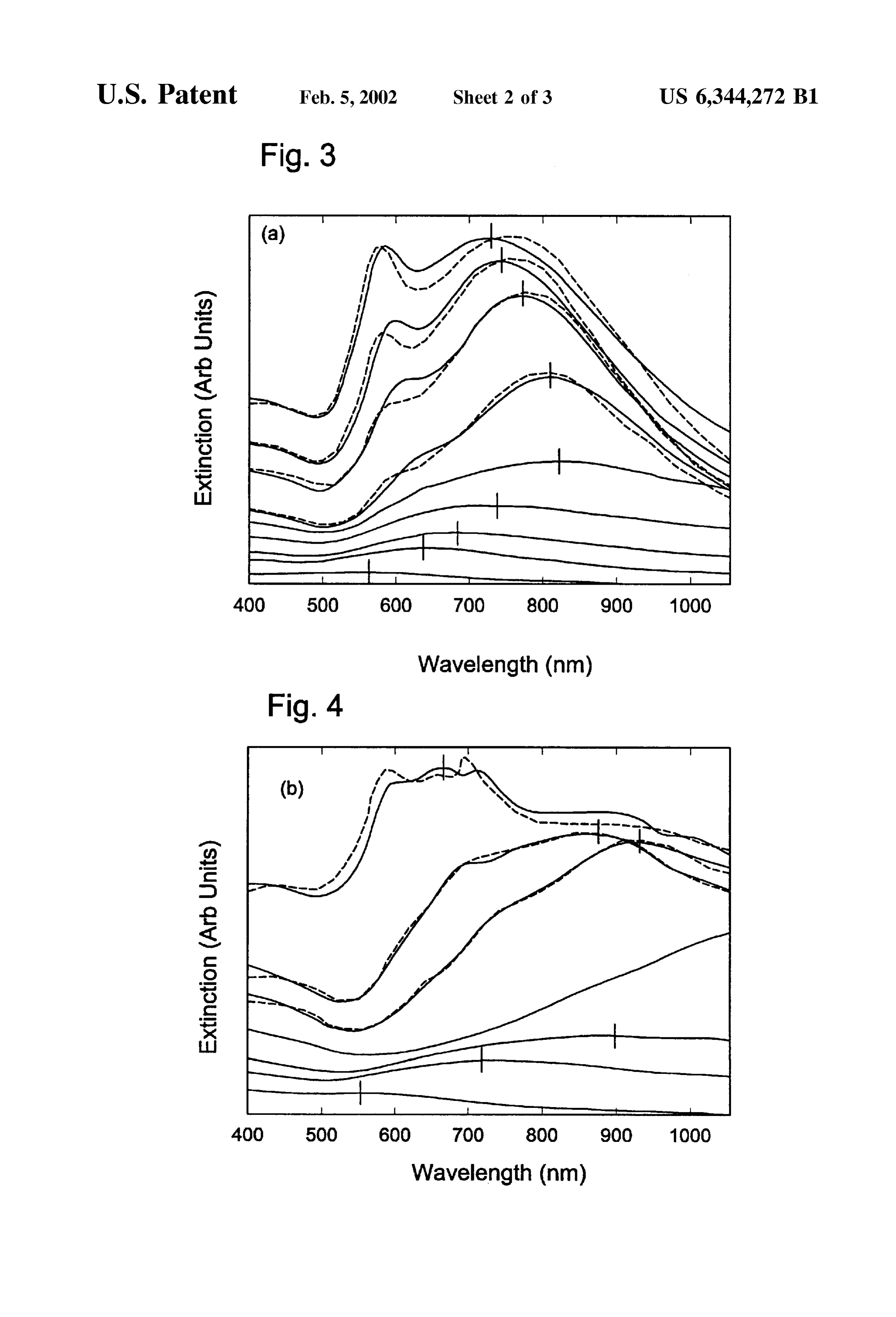
radius/Shell thickness ratioS. 40 The method of Stober (1968), incorporated herein by FIG. 2: Calculation of optical resonance wavelength reference to the extent it provides Such methods, was used Versus core radius/Shell thickness ratio for metal nanoshells to produce monodisperse Silicon dioxide particle cores. (Silica core with gold shell in water). Tetraethyl orthosilicate (TEOS) 99.999% was obtained from FIG. 3: Growth of gold shell on 120 nm diameter silica Aldrich Chemical Co., Sodium hydroxide was from Fluka core particles. The lower spectral curves follow the evolu 45 Chemical Co. and highly purified water was obtained from tion of the optical absorption as coalescence of the gold layer a Millipore “TOTALO" system that included “MILLIO.' progresses. Corresponding theoretical peaks are plotted with and “MILLIO'” filters. All glassware was cleaned with dotted lines. From right to left these spectra correspond to chromic acid Solution and thoroughly rinsed with theoretical shell thicknesses of 14, 17, 24 and 30 nm. “TOTALO' water.
Experimental shell thicknesses determined by TEM were 50 Variations in water, base concentration, and TEOS con 20, 26, 29, 33 nm+/-4 nm. centration were used to produce monodisperse Silica spheres FIG. 4: Growth of gold shell on 340 nm diameter silica of various sizes. Temperature and electrolyte concentration core particles. The dotted lines from right to left correspond also affected the final diameter of the particles. Generally, to calculations with shell thicknesses of 17, 35, and 48 nm. the following concentration ranges were used: 0.1 to 0.5 M TEM determined shell thicknesses were 18, 39, and 53 55 TEOS, 0.5 to 17 M HO, and 0.5 to 3.0 M ammonia. In nim--f-12. addition, a variety of alcohols were used as Solvents, FIG. 5: Absorption spectrum of mixture of particles that however, ethanol was preferred. Higher ammonia concen would absorb or Scatter all wavelengths of Solar radiation trations provide larger particles.
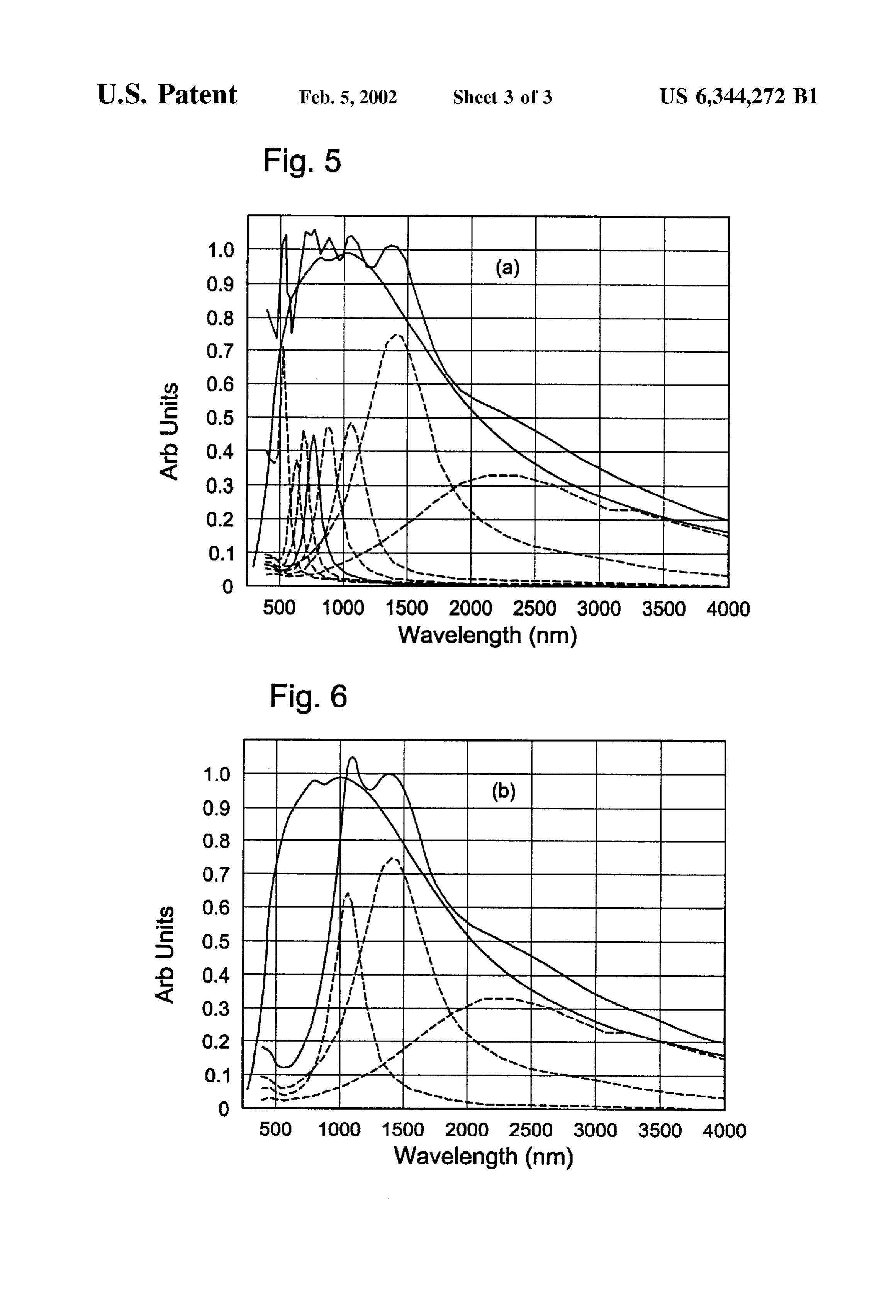
available at the earth's Surface. Uniform particles having a diameter of 120 nm as mea FIG. 6: Absorption spectrum of mixture of particles that 60 sured by a transmission electron microscope (TEM) were would absorb or scatter only the infrared wavelengths of prepared by the following method. Approximately 50 mil Solar radiation available at the earth's Surface. liliters (ml) of dry (100%) ethanol and 4 ml of NHOH (25%
DETAILED DESCRIPTION OF THE
NH in water), were stirred in a glass beaker. To this
INVENTION
Solution, 2.2 ml of tetraethyl orthosilicate having a purity of 65 at least 99.999% was added and allowed to stir for at least
The following examples are offered by way of illustration 8 hours. By varying the concentrations of NHOH, water and are not intended to limit the invention in any manner. In and Silicate among other factors, the size of the Silica particle
Page 11
was varied from approximately 20 nm to 500 nm diameter. by reference to the extent Such methods are disclosed. A Larger core particles were grown using a Seeded growth Solution of 45 ml of water, 300 microliters of 1M NaOH and technique where additional TEOS and water were added to 1 mL of a freshly diluted 1% acqueous solution of tetrakis already formed silica particles. Multiple additions of small (hydroxymethyl)phosphonium chloride (THPC) was stirred amounts of additional reactants allowed monodisperse core in a 100 ml flat bottom beaker with a pyrex coated magnetic particles to be grown as large as 4 microns. stir bar. After 2 minutes, 2 ml of chloroauric acid (25 mM
EXAMPLE III
dark-aged Stock Solution, hydrogen tetrachloroaurate (III) trihydrate 99.999% from Aldrich) was added. This reaction
Linker Molecule Attachment mix was used to form gold particles in Solution with an To assemble a metallic Shell around an inner layer fre average particle diameter of 1–2 nm. To increase the size of quently required the use of linker molecules. These mol the particles higher concentrations of gold chloride could be ecules were chemically linked to the inner layer and Served used. Particles prepared in this fashion were referred to as to bind atoms, ions, atomic or molecular clusters of the ultra Small gold particles or (UG). conducting Shell to the inner layer. The conducting shell Generally, the UG solution was mixed with silica particles 15 in an amount that would theoretically cover the core particle atoms that bound to the linkers were used as nucleation Sites for reduction of the additional atoms or molecules to com Surface five to ten times. The Solution was allowed to react plete the shell. One method used to attach gold particles to for 3 hours under gentle Stirring. In the preferred embodi Silicon dioxide was to treat the particles with aminopropy ment the gold was used 5-30 days after it was made. ltriethoxy silane (APTES). The silanol end groups of the Typically, after three hours, unreacted gold colloid was APTES molecules attach covalently to the silica core Separated from the gold-decorated Silica particles by cen extending their amine groups outward as a new termination trifugation at 1000 RCF. The minimum amount of centrifu of the particle Surface. gal force required to effect Separation was used to avoid In this method, 10 ml of a Silica particle Suspension Such coalescence of the particles. Particles were washed twice by as prepared in Example III, was added to a 50 ml glass resuspension and centrifugation.
beaker. Next, pure aminopropyltriethoxy silane (APTES) 25 The inventors made the Surprising discovery that the gold was added to the Solution. Based on estimates, enough Silane decorated particles did not aggregate after being centrifuged was added to coat the particles with multiple layers of Silane. and redispersed in the absence of additional Stabilizing For example, 40 microliters of undiluted APTES was used compounds. This discovery allowed the convenient Separa for particles having diameters of 120 nm. The solution was tion of the decorated Silica from colloidal gold, leaving the stirred for 2 hours, diluted to 200 mls and then heated to a gold attached to Silica in a chemically reactive State. Various boil for four hours. The heating Step promotes the reaction protectants could be added before centrifugation to facilitate of silanol groups into Si-O-Si bonds and strengthens the later resuspension of the particles. These protectants include attachment of the Silane to the Silica. This mixture was polyvinyl alcohol, polyethylene glycolor phosphine ligands, centrifuged at 2000xg for 30 minutes. The Supernatant was and thiol-terminated carboxylic acid linkages. Resuspension decanted off and the pellet was redispersed ultrasonically. 35 was easily accomplished when a minimum amount of force This washing procedure was repeated five times. was used in the centrifugation Step and any aggregates of Many linker molecules other than aminopropyl triethoxy particles could be redispersed by treatment with Sonification. Silane are Suitable for use in this procedure. For example, A dynamic light Scattering instrument was used according to aminopropyl trimethoxy Silane, diaminopropyl diethoxy standard and well known methods to verify that the particles Silane, or 4-aminobutyl dimethylmethoxysilane and the like 40 were dispersed. The dispersed particles were diluted to 10 can be used. In addition, the Surface can be terminated with mls and used as a Stock Solution for the growth of the a linker that allows for the direct reduction of metal atoms complete metal shell.
on the Surface rather than through a metallic cluster inter EXAMPLE V me diary. In other embodiments, reaction of Growth of the Shell tetrahydrothiophene(AuCl) with a silica core coated with 45 The metal clusters were enlarged by deposition of gold diphenyltriethoxy Silane leaves a Surface terminated with using a variety of reductants Such as hydroxylamine gold chloride ions which can provide Sites for additional hydrocholoride, sodium borohydride, and formaldehyde. gold reduction. In other embodiments, a thin Shell of another Formaldehyde was preferred. A solution of 25 mg anhydrous nonmetallic material, Such as CdS or CdSe grown on the potassium carbonate was added to 100 ml of water contain exterior of a silica particle allows for a metallic shell to be 50 ing 1.5 ml of 25 mM chloroauric acid solution (PCG). This reduced directly onto the nanoparticle's Surface. In other Solution was allowed to age in the dark for one day. embodiments, functionalized oligomers of conducting poly Approximately 10 ml+/-5 ml of PCG was rapidly stirred mers can be attached in Solution to the functionalized or nonfunctionalized Surface of the core nanoparticle and Sub with 2-5 mls of the gold clustered silica solution. A 100 microliter aliquot of freshly prepared formaldehyde Solution
Sequently cross-linked by thermal or photo-induced chemi 55 (2% by volume in water) was slowly added. cal methods.
Before enlargement of the metal clusters, the metal clus
EXAMPLE IV ters attached to the particles had the same UV-visible Attachment of Metal Clusters absorption spectrum as their natural colloidal form. AS Metal clusters were attached to the linker molecules on additional metal was deposited onto the clusters, the absor the core by immersing the derivatized core particles in a 60 bance maximum of the particle shifted to longer metal colloid bath. Any metal that can be made in colloidal wavelengths, as shown in the lower curves of FIGS. 3 and form could be attached as a metal cluster. For example, 4. When the gold shell was complete, the particles absor Silver, platinum, palladium, lead and the like could be used. bance maximum was related to its geometry, Specifically, to In addition, metal-like organic molecules are Suitable. Such the ratio of the thickness of the inner nonconducting layer to compounds include polyacetylene and polyaniline. Gold 65 the thickness of the outer conducting layer. AS the conduct clusters having a diameter of 1-3 nm were grown using the ing layer grew thicker, the absorbance maximum of the reduction reaction as described by Duff, incorporated herein particle shifted to shorter wavelengths, as shown in the
Page 12
upper curves of FIGS. 3 and 4. The progress of this reaction combined spectra of three distinct particles having varied was followed spectrophotometrically and terminated when core to shell ratioS in a particle mixture and that absorb the desired wavelength for the absorbance maximum was distinct Segments of the Solar radiation Spectrum. These obtained. Typically a color change occurred within 10 particles may be a subset of the mixture of Example VI. minutes. For 110 nm diameter core particles, typically a Such a mixture can be incorporated into polymers, Visible color change is apparent, from faint brown to purple, glasses, paints, epoxies, or other coating matrices by Stan blue, green, or yellow. Some of the other factors that dard methods well known in the art. The thermal properties influenced the optical absorption of the Spectrum are the size of these materials can then be used in appropriate applica of the core, the roughness of the shell, the shape of the core, tions time that rely on trapping Solar energy while at the same allowing visible wavelengths to pass. Such materials additional reactants in Solution that may be incorporated into could be incorporated the core during the reduction, the continuity of the shell, and trap Some fraction ofinto Sunroofs and windows that would incident radiation from a Solar or the degree of aggregation of the particles. nonsolar Source while allowing a clear field of vision. Many different methods can be used to complete the metal Similarly incorporation of these particles into heat resistant shell once the nucleation sites are in place. One of skill in the paint would allow for the production of colored paints that art will realize that any method that can be used to develop 15 have the ability to absorb or to scatter most of the Sun's heat a metal colloid into a larger metal colloid should be Suc energy.
cessful for the shell growth. For example, silver solutions Similarly, it is possible to engineer “transmission win such as the commercially available LI silver from dows' through which Selected wavelengths of electromag Nanoprobes, Inc. may work. In addition, it is not necessary netic radiation can pass and incorporate those particles into that the tethered Seed particle be of the same material as the Similar materials. It is also possible to engineer materials shell material. In one embodiment Silver nitrate is reduced that will Strongly absorb or Scatter over a specific wave onto Silica coated with UG. This is done in a basic Solution length range corresponding to the operating range of a laser with formaldehyde as a reductant and results in a Silver Shell. or lasers, and be either translucent or transparent below and Photo-induced deposition of the metal shell onto the pre above the Specific wavelength range. This type of material pared nanoparticle Surface is also possible. 25 could be used for eye protection in the presence of a laser Direct reduction of Silver onto a non-conducting core can SOUICC O SOUCCS.
be accomplished with the reduction of silver directly onto a EXAMPLE VIII CdS semiconductor layer. In order to construct a CdS with Nanoengineered Solar Cells a diameter greater than 20 nm it was necessary to first grow Current Solar energy cells only convert a Small fraction of a CdS layer onto a Silica core. This can be accomplished the Sun's radiant energy into electrical energy. Clearly, using water in oil microemulsions, for example. In one converting absorbed radiation from acroSS the entire Solar embodiment silver was reduced onto a silica/CdS particle by Spectrum into electricity would achieve higher Solar cell adding the particles to a Solution of AgNO, and NH and efficiencies than is currently available. The present embodi then slowly adding a NH-OHCl solution to develop the ment relies on the electron accepting capability of thin Solid shell. 35 films of buckministerfullerene or Co., a spherical carbon
EXAMPLE VI cage molecule. The photovoltaic effect of Coo based thin Nanoengineered Thermal Management Materials and Coat film, which is enhanced by forming a heterojunction with a conducting polymer film, Such as PPV, is Sensitized to an ings enhanced photoresponse at longer wavelengths by introduc The present application takes advantage of the fact that 40 ing a layer of Suitably designed the Sun's maximum radiant power that reaches the Earth's the Co and the PPV. A dilute metal or nanoshells between dense layer of metal surface is distributed broadly across the visible and infrared nanoshells is embedded at the interface between regions of the electromagnetic spectrum and a mixture of ducting polymer and the Co. The electroStatic fieldthecreated con nanoparticles can be developed to either absorb or Scatter by the heterojunction establishes an assymetric potential energy throughout that entire Spectrum. The present tech 45 acroSS the metal nanoshell layer. The Strong electron donor nology is the only method known for Systematic control of acceptor interaction between the metal-like conductor of the absorption or Scattering of radiation across the entire range of the Solar emission spectrum. In FIG. 5 is shown an shell layer and the Co will cause the metal-like conductor example of a mixture of the present embodiments that can of the shells to inject electrons into the Co layer when the absorb the entire Solar spectrum. In this Figure is shown the 50 shell their layers are illuminated with radiation corresponding to absorption resonance. The released electrons are individual spectra of eight particles having varied core to detected as either a photocurrent or photovoltage by meth shell ratioS and that absorb distinct Segments of the Solar ods known in the art. Such a device could be made using radiation Spectrum. A mixture of these particles is capable of Spun polymer films, vacuum deposition, or other methods absorbing radiation acroSS the entire Solar spectrum. known to one skilled in the art. Any pair of electron Such a mixture can be incorporated into polymers, glasses, paints, epoxies, or other coating matrices by Stan 55 donor-acceptor materials that could be sequentially depos dard methods well known in the art. The thermal properties ited into Such a layer Structure could be used with metal of these materials can then be used in appropriate applica consist of asmore nanoshells photosensitive devices. This device may also tions that rely on absorption and Scattering of Solar energy nanoshell/electronthan one layer of electron donor/metal or any Source of electromagnetic radiation across the wave 60 It will be readily apparentlayers.
acceptor to one skilled in the art that length range of the mixture. various Substitutions and modifications may be made to the EXAMPLE VII invention disclosed herein without departing from the Scope Nanoshell Windows and Spirit of the invention. For example, the nanoparticle In FIG. 6 is shown an example of a mixture of the present core used not be spherical and may retain other shapes. Such embodiments that can absorb the entire infrared region of 65 as planar sheets. Similarly, the invention may be employed the Solar spectrum while allowing visible light from the Sun to place metal nanoshells on planar sheets and other Sur to pass through. In this Figure is shown the individual and faces.
Page 13
EXAMPLE IX Daniel G. Duff, Alfons Baiker, Ian Gameson, and Peter P. Optically Active Materials with Metal Nanoshell Dopants Edwards (1993) Langmuir 9, 2310-2317. A New Hydro The adjustable plasmon resonance of metal nanoshells sol of Gold Clusters. 2. A Comparison of Some Different can be used as dopants or additives to influence and modify Measurement Techniques.
the optical properties of optically active host materials, Such 5 Jovan Nedeljkovic and Ramesh C. Patel (1991) Appl. Phys. as, but not limited to, conducting polymers or organic Lett. 58, 2461-2463. Observation of Plasmon-Enhanced Semiconductors. The nanoshell resonance can be designed to Optical Extinction in Silver-Coated Silver Bromide overlap with either the Singlet or the triplet eXciton reso Nanoparticles.
nances of the host material. Since metal nanoparticle reso M. J. Puska and R. M. Nieminen, (1993) Physical Review A nances have excitation lifetimes of only a few picoSeconds, 47, 1181-1186. Photoabsorption of atoms inside C60. any donor-acceptor interaction between the comparatively Werner Stober, Arthur Fink, and Ernst Bohn, (1968) J. long-lived excitons of the conducting polymer and the Colloid and Interface Science 26, 62-69. Controlled nanoparticles will result in Strong quenching of the Specific Growth of Monodisperse Silica Spheres in the Micron excitation or excitations of the host material to which the Size Range.
nanoshell resonance has been tuned. This provides a method 15 H. S. Zhou, I. Honma, and H. Komiyama, and J. W. Haus, for Strongly modifying the optical properties of a material (1994) Phys. Rev., 50, 12,052-12,056. Controlled Syn with little modification of its chemical properties. thesis and Quantum-Size Effect in Gold-Coated Nanopar
Optically Active Species Inside Metal Nanoshell Nanocavi R. D. Averitt, D. Sarkar, and N. J. Halas, (1997) Phys. Rev. ties Lett. 78, 4217-4220. Plasmon Resonance Shifts of A straightforward variation of the fabrication method Au-Coated Au2S Nanoshells: Insight into Multicompo nent Nanoparticle Growth.
outlined above enables the insertion of optical absorbers and K. V. Sarathy, G. Raina, R. T. Yadav, G.U. Kulkarni, and C. luminescent Species into the dielectric cores of metal N. R. Rao, (1997), J. Phys. Chem. B., 101,9876–9880. nanoshells. Procedures for bonding functionalized dye mol ecules into Silica nanoparticles grown by the Stober method 25 Thiol-Derivatized and Platinum.
Nanocrystalline Arrays of Gold, Silver, have been demonstrated by van Blaaderen and Vrij, incor U. Kreibig, M. Gartz, and A. Hilger, (1997), Berichte der porated herein by reference to the extent it discloses Such Bunsen-Gesellchaft fur Physikalische Chemie, 101, methods. Introducing an optically absorbing Species into the 1593–1603. Mie Resonances: Sensors for Physical and core will Strongly influence the plasmon resonance shift and Chemical Cluster Interface Properties. width. Conversely, the optical field enhancement within the A. van Blaaderen and A. Vrij, (1992), Langmuir, 8, metal "nanocavity” modifies the absorption and fluorescent 2921-2925. Synthesis and characterization of colloidal properties of the chromophores incorporated within this dispersions of fluorescent, monodisperse Silica Spheres. nanoStructure. What is claimed is:
EXAMPLE XI 1. A nanoparticle comprising at least one non-conducting Metal Nanoshell Structures Via Planar Fabrication Methods 35 core layer and at least one conducting shell layer, Said shell There also exists the possibility of fabricating spherical, layer immediately adjacent to and independently layered hemispherical, or other types of geometries directly from upon Said core layer, wherein thickness of Said shell layer is planar Semiconductor or dielectric Surfaces. For example, on not limited to account for the bulk dielectric properties of a Silicon Substrates Specific chemical etching techniques result material comprising Said conducting shell layer, Said nano in well-defined nanoscale Structures extending up from the 40 particle having a wavelength extinction maximum between Surface of the Substrate. Using the unique methods described 300 nm and 20 lum.
herein, Such nanostructures can be metal-coated, resulting in 2. The nanoparticle of claim 1 wherein Said conducting devices or regions of devices with unique properties. For shell layer comprises a metal.
example, an array of nanometer-sized hemispheres etched 3. The nanoparticle of claim 2 wherein said metal is onto a Silicon Substrate could be coated with a thin layer of 45 comprised of a metal Selected from the group consisting of gold. Such a Substrate would have the same optical tunabil the coinage metals, noble metals, transition metals, and ity as nanoshells, that is, the optical absorption of the Synthetic metals.
substrate would have a resonance defined by the size of the 4. The nanoparticle of claim 1 wherein Said conducting hemispheres and the thickness of the metal layer. Such shell layer comprises an organic conducting material. Substrates would be useful as SERS-based chemical sensors. 50 5. The nanoparticle of claim 1 wherein Said conducting Similarly, nanoshells attached or directly formed onto small shell layer comprises a metal alloy. cantilevers, Such as those used in Scanning force 6. The nanoparticle of claim 1 wherein Said nanoparticle microScopy, could be used as Small localized probes for the comprises at least one additional non-conducting core layers wavelength-Specific detection of radiation: in this in an alternating Sequence with additional conducting shell embodiment, the deflection or the vibrational frequency of 55 layers.
the cantilever may be monitored with either response being 7. The nanoparticle of claim 1 wherein said non proportional to the absorbed energy content of the nanoshell conducting core layer comprises a dielectric material. or nanoshells attached or fabricated onto the cantilever 8. The nanoparticle of claim 7 wherein said dielectric Structure. Such microbolometers would find applications in material is Selected from the group consisting of Silicon a variety of diagnostic environments requiring localized 60 dioxide, titanium dioxide, PMMA, polystyrene, and den optical detection, or optical detection by a very Small drimerS.
(micron-sized) structure. 9. The nanoparticle of claim 1 wherein said non
REFERENCES CITED
conducting core layer comprises a Semi-conducting mate rial.
Meyer H. Birnboim and Arthur K. Noeves, U.S. Pat. No. 65 10. The nanoparticle of claim 1 wherein said non 5,023,139 issued Jun. 11, 1991; Nonlinear Optical Mate conducting core layer comprises an organic molecule or an rials. organic Supermolecular structure.
Page 14
11. The nanoparticle of claim 1 wherein said non 34. A particle comprising a core that is between 1 nm and conducting core layer comprises a mixture of non 2 um in diameter, Said core further comprising Silicon conducting materials. dioxide, Said core being encapsulated by a layer of a metal 12. The nanoparticle of claim 1 wherein said non that is less than approximately 40 nm thick, Said metal conducting core layer comprises an optically absorbing comprising gold, wherein Said metal is linked to Said core material. through a linker molecule, Said particle having a wavelength 13. The nanoparticle of claim 1 wherein said non absorbance maximum between 300 nm and 20 lum.
conducting core layer comprises a fluorescent material. 35. A particle that absorbS electromagnetic radiation, Said 14. The nanoparticle of claim 1 further comprising an particle having a diameter of greater than approximately 1 outermost non-conducting core layer bound to an adjacent nm. and comprising at least a first and a Second layer, Said conducting shell layer.
15. The nanoparticle of claim 1 further comprising a Secondcomprises layer Surrounding Said first layer, wherein Said first non-conducting layer Sandwiched between two conducting layer layer comprises a non-conducting material and Said Second a conducting material, and wherein thick layers.
16. The nanoparticle of claim 1 further comprising a 15 neSS of Said Second layer is not limited to account for the conducting layer Sandwiched between two non-conducting bulk dielectric properties of a material comprising Said layers. Second layer.
17. The nanoparticle of claim 1 wherein the diameter of 36. A mixture of nanoparticles as in claim 1, Said mixture said nanoparticles varies by less than 100%. capable of absorbing electromagnetic radiation, Said mixture 18. The nanoparticle of claim 1 wherein said conducting further comprising nanoparticles between approximately 5 shell layer coats at least 10% of Said non-conducting core nm and 2 um thick.
layer. 37. The particle of claim 34, wherein said linker molecule 19. The nanoparticle of claim 10 wherein said conducting further comprises aminopropyltriethoxy Silane. shell layer coats at least 10% but less than 100% of said further 38. The particle of claim 34, wherein said linker molecule non-conducting core layer. 25 comprises aminopropyltrimethoxy Silane. 20. The nanoparticle of claim 1 wherein Said conducting 39. The particle of claim 34, wherein said linker molecule shell layer completely Surrounds Said non-conducting core further comprises diaminopropyl diethoxy Silane. layer. 40. The particle of claim 34, wherein said linker molecule 21. The nanoparticle of claim 1 wherein Said conducting further comprises 4-aminobutyl dimethylmethoxysilane. shell layer is linked to Said non-conducting core layer by a 41. The particle of claim 34, wherein said linker molecule linker molecule. further comprises a linker upon which direct reduction of 22. The nanoparticle of claim 1 wherein Said nanopar atoms of Said metal may be conducted.
ticles is approximately Spherical. 42. The particle of claim 34, wherein said linker molecule 23. The nanoparticle of claim 1 wherein Said nanoparticle further comprises diaminopropyl diethoxy Silane. is non-spherical. 35 43. The particle of claim 34, wherein said linker molecule 24. An X-ray absorbing device comprising the nanopar further comprises diphenyltriethoxy Silane reacted with ticle of claim 1. tetrahydrothiophene(AuCl).
25. A light detecting device comprising the nanoparticle 44. The particle of claim 34, wherein said linker molecule of claim 1. further comprises a Second non-metallic material. 26. A chemical Sensing device comprising the nanopar 40 45. The particle of claim 44, wherein said second non ticle of claim 1. metallic material further comprises either CdS or CdSe. 27. Abolometer comprising the nanoparticle of claim 1. Said46.linker
The particle of any of claims 34 and 44-45, wherein molecule is crosslinked to another linker mol 28. A microbolometer comprising the nanoparticle of ecule.
claim 1.
29. A Sensing cantilever device comprising the nanopar 45 47. The particle of claim 46, wherein said crosslinked ticle of claim 1. linker molecules are crosslinked by a thermal or a photo 30. Adopant in an optically active material comprising the induced chemical crosslinking process. nanoparticle of claim 1. 48. The particle of claim 34, wherein said wavelength 31. A polymer comprising the nanoparticle of claim 1. absorbance maximum is between 500 nm and 10 um. 32. A photovoltaic Solar cell comprising the nanoparticle 50 49. The particle of claim 34, wherein said wavelength of claim 1. absorbance maximum is between 900 nm and 5 lum. 33. An infrared detector comprising the nanoparticle of claim 1.
Page 15
UNITED STATES PATENT AND TRADEMARK OFFICE
CERTIFICATE OF CORRECTION
PATENT NO. : 6,344,272 B1 Page 1 of 7
INVENTOR(S) : Oldenburg, Steven J., Averitt, Richard D. and Halas, Nancy J.
It is certified that error appears in the above-identified patent and that said Letters Patent is hereby corrected as shown below:
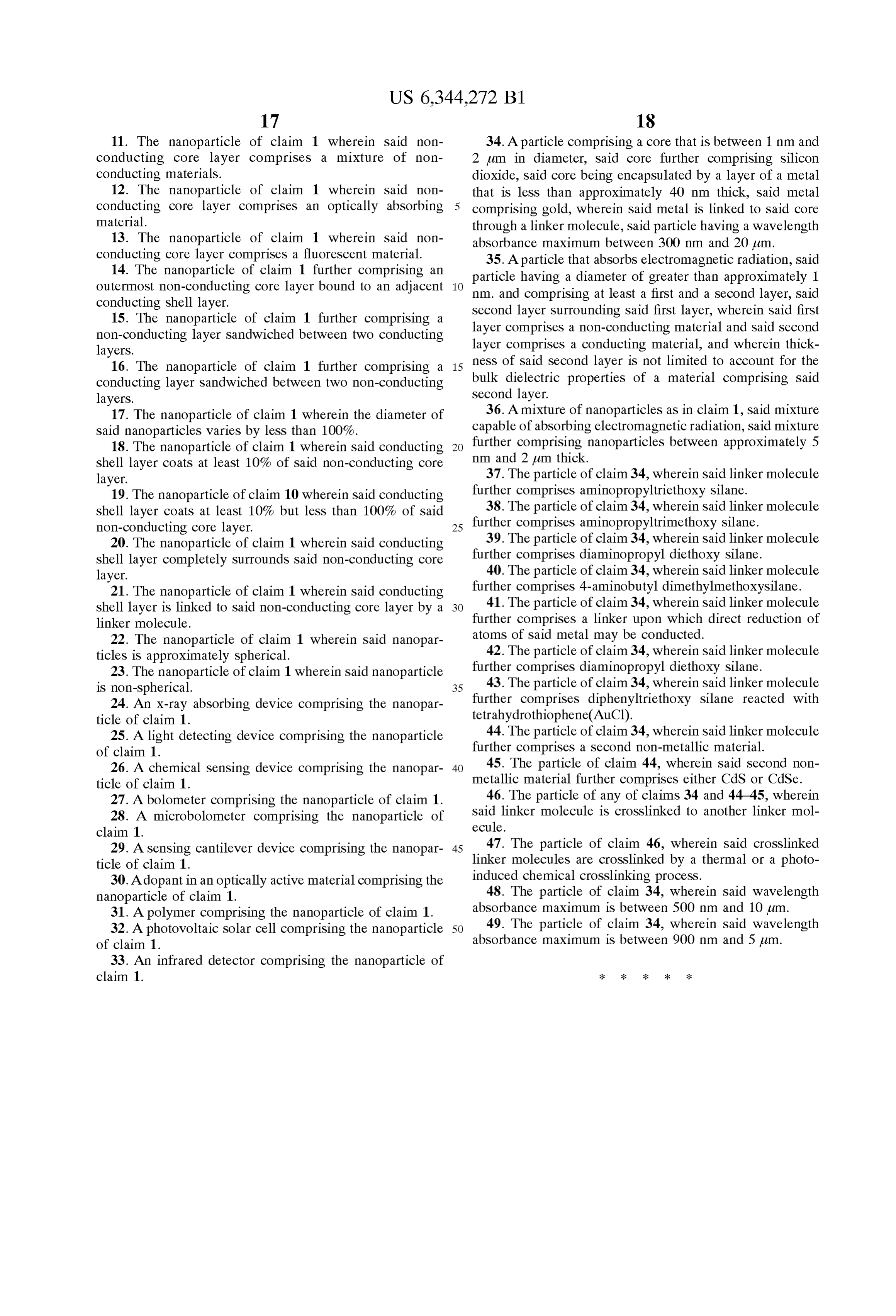
Column 16
Beginning at line 34, delete all claims and replace with claims 1-54 as follows: 1. A nanoparticle comprising at least one non-conducting core layer and at least one conducting Shell layer, Said Shell layer independently layered upon Said core layer, Such that the thickness of said shell layer is independent of the radius of Said core layer wherein the thickness of Said shell layer is less than that of a shell layer whose dielectric properties are described by a bulk dielectric function of a material comprising said conducting shell layer and is not limited to account for the bulk dielectric properties of a material comprising Said conducting Shell layer said nanoparticle having a wavelength extinction maximum between 300 nm and 20um. 2. The nanoparticle of claim 1 wherein said conducting shell layer comprises a metal. 3. The nanoparticle of claim 2 wherein said metal is comprised of a metal Selected from the group consisting of the coinage metals, noble metals, transition metals, and Synthetic metals Such as polyacetylene and polyanaline.
4. The nanoparticle of claim 1 wherein said conducting shell layer comprises a metal-like organic conducting material.
5. The nanoparticle of claim 1 wherein said conducting shell layer comprises a metal alloy. 6. The nanoparticle of claim 1 wherein said nanoparticle comprises at least one additional non-conducting core layerS in an alternating Sequence with additional conducting Shell layerS. 7. The nanoparticle of claim 1 wherein said non-conducting core layer comprises a dielectric material.
Page 16
UNITED STATES PATENT AND TRADEMARK OFFICE
CERTIFICATE OF CORRECTION
PATENT NO. : 6,344,272 B1 Page 2 of 7
INVENTOR(S) : Oldenburg, Steven J., Averitt, Richard D. and Halas, Nancy J.
It is certified that error appears in the above-identified patent and that said Letters Patent is hereby corrected as shown below:
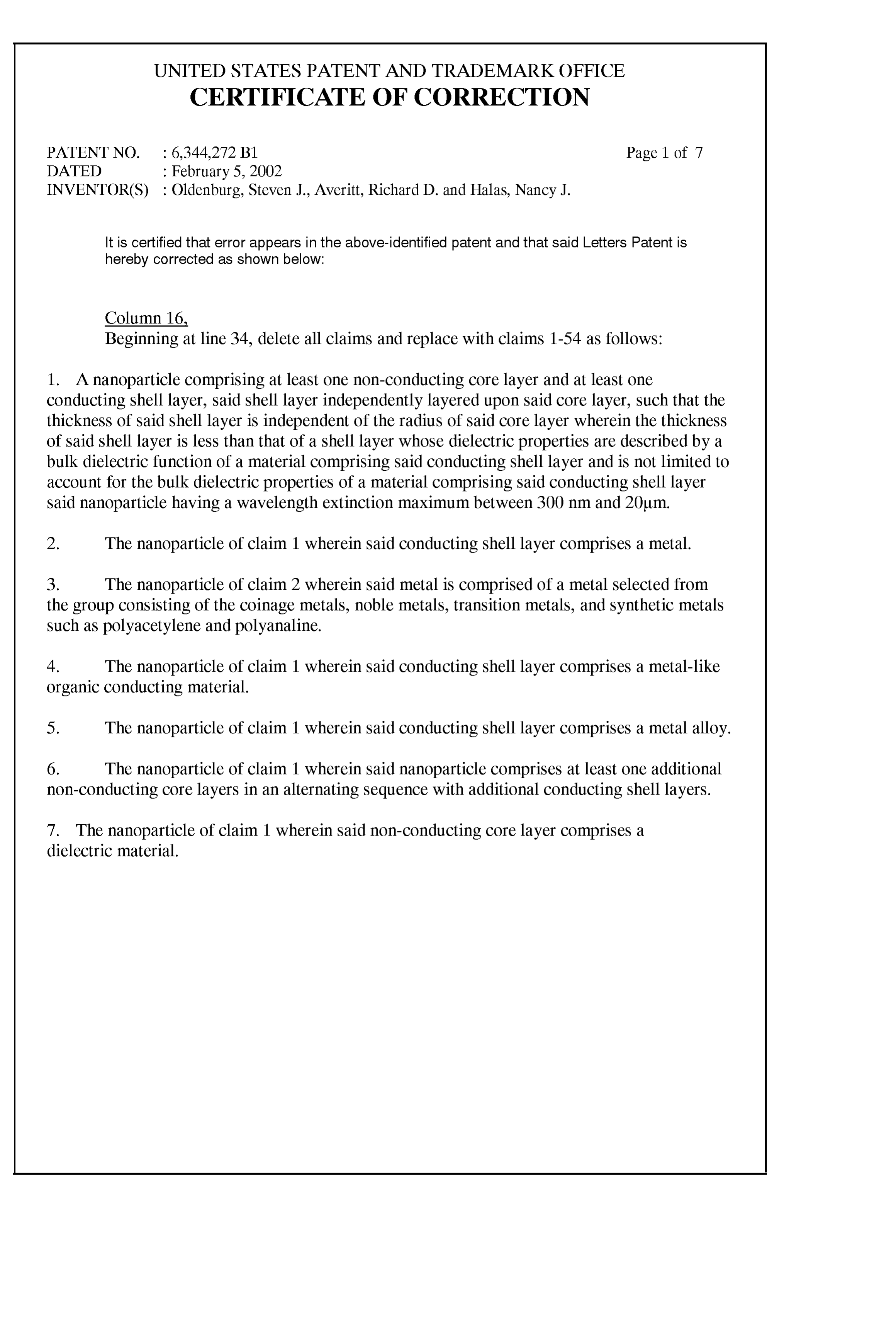
8. The nanoparticle of claim 7 wherein said dielectric material is selected from the group consisting of silicon dioxide, titanium dioxide, PMMA, polystyrene, and dendrimers. 9. The nanoparticle of claim 1 wherein Said non-conducting core layer comprises a Semi-conducting material.
10. The nanoparticle of claim 1 wherein said non-conducting core layer comprises an organic molecule or an organic Supermolecular Structure.
11. The nanoparticle of claim 1 wherein Said non-conducting core layer comprises a mixture of non-conducting materials.
12. The nanoparticle of claim 1 wherein Said non-conducting core layer comprises an optically absorbing material.
13. The nanoparticle of claim 1 wherein said non-conducting core layer comprises a fluorescent material.
14. The nanoparticle of claim 1 further comprising an Outermost non-conducting core layer bound to an adjacent conducting Shell layer.
15. The nanoparticle of claim 1 further comprising a non-conducting layer Sandwiched between two conducting layers.
16. The nanoparticle of claim 1 further comprising a conducting layer Sandwiched between two non-conducting layerS.
17. The nanoparticle of claim 1 wherein the diameter of Said nanoparticles varies by less
18. The nanoparticle of claim 1 wherein said conducting shell layer coats at least 10% of Said non-conducting core layer.
Page 17
UNITED STATES PATENT AND TRADEMARK OFFICE
CERTIFICATE OF CORRECTION
PATENT NO. : 6,344,272 B1 Page 3 of 7
INVENTOR(S) : Oldenburg, Steven J., Averitt, Richard D. and Halas, Nancy J.
It is certified that error appears in the above-identified patent and that said Letters Patent is hereby corrected as shown below:
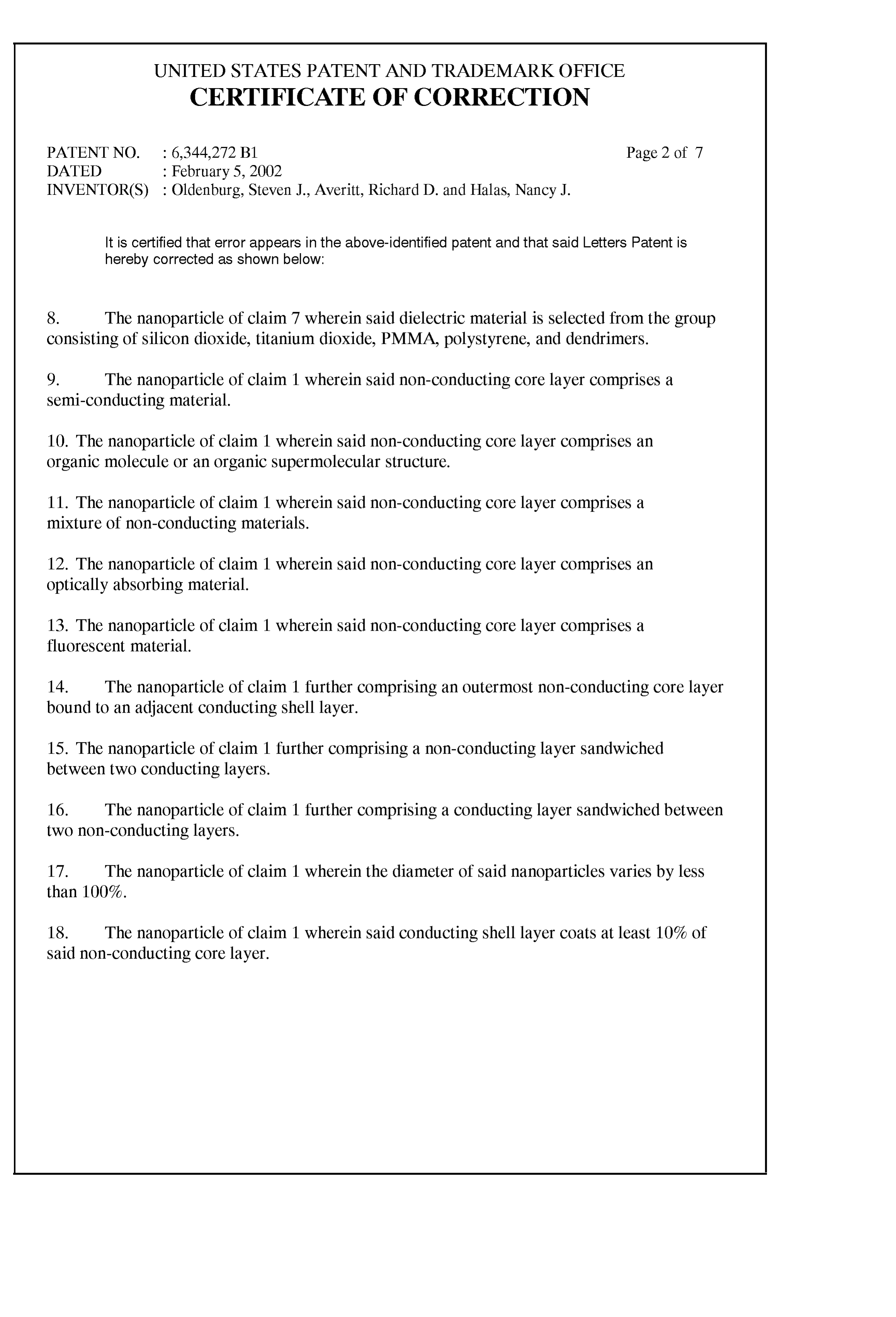
19. The nanoparticle of claim 10 wherein said conducting shell layer coats at least 10% but less than 100% of Said non-conducting core layer 20. The nanoparticle of claim 1 wherein said conducting shell layer completely surrounds Said non-conducting core layer.
21. The nanoparticle of claim 1 wherein said conducting shell layer is linked to said non-conducting core layer by a linker molecule.
22. The nanoparticle of claim 1 wherein said nanoparticle is approximately spherical. 23. The nanoparticle of claim 1 wherein said nanoparticle is non-spherical. 24. An X-ray absorbing device comprising the nanoparticle of claim 1. 25. A light detecting device comprising the nanoparticle of claim 1. 26. A chemical Sensing device comprising the nanoparticle of claim 1. 27. A bolometer comprising the nanoparticle of claim 1.
28. A microbolometer comprising the nanoparticle of claim 1.
29. A Sensing cantilever device comprising the nanoparticle of claim 1. 30. A dopant in an optically active material comprising the nanoparticle of claim 1. 31. A polymer comprising the nanoparticle of claim 1.
32. A photovoltaic Solar cell comprising the nanoparticle of claim 1. 33. An infrared detector comprising the nanoparticle of claim 1.
Page 18
UNITED STATES PATENT AND TRADEMARK OFFICE
CERTIFICATE OF CORRECTION
PATENT NO. : 6,344,272 B1 Page 4 of 7
INVENTOR(S) : Oldenburg, Steven J., Averitt, Richard D. and Halas, Nancy J.
It is certified that error appears in the above-identified patent and that said Letters Patent is hereby corrected as shown below:
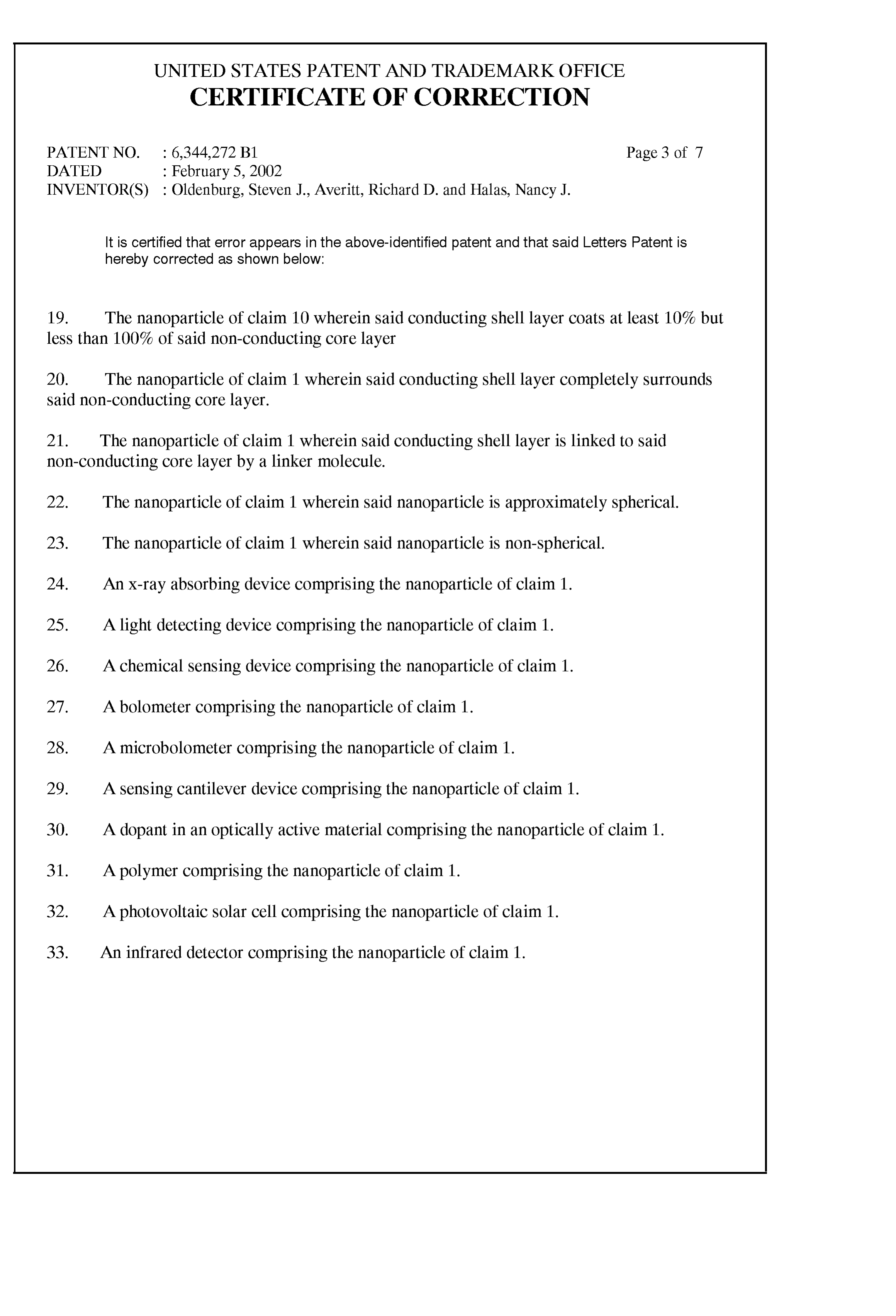
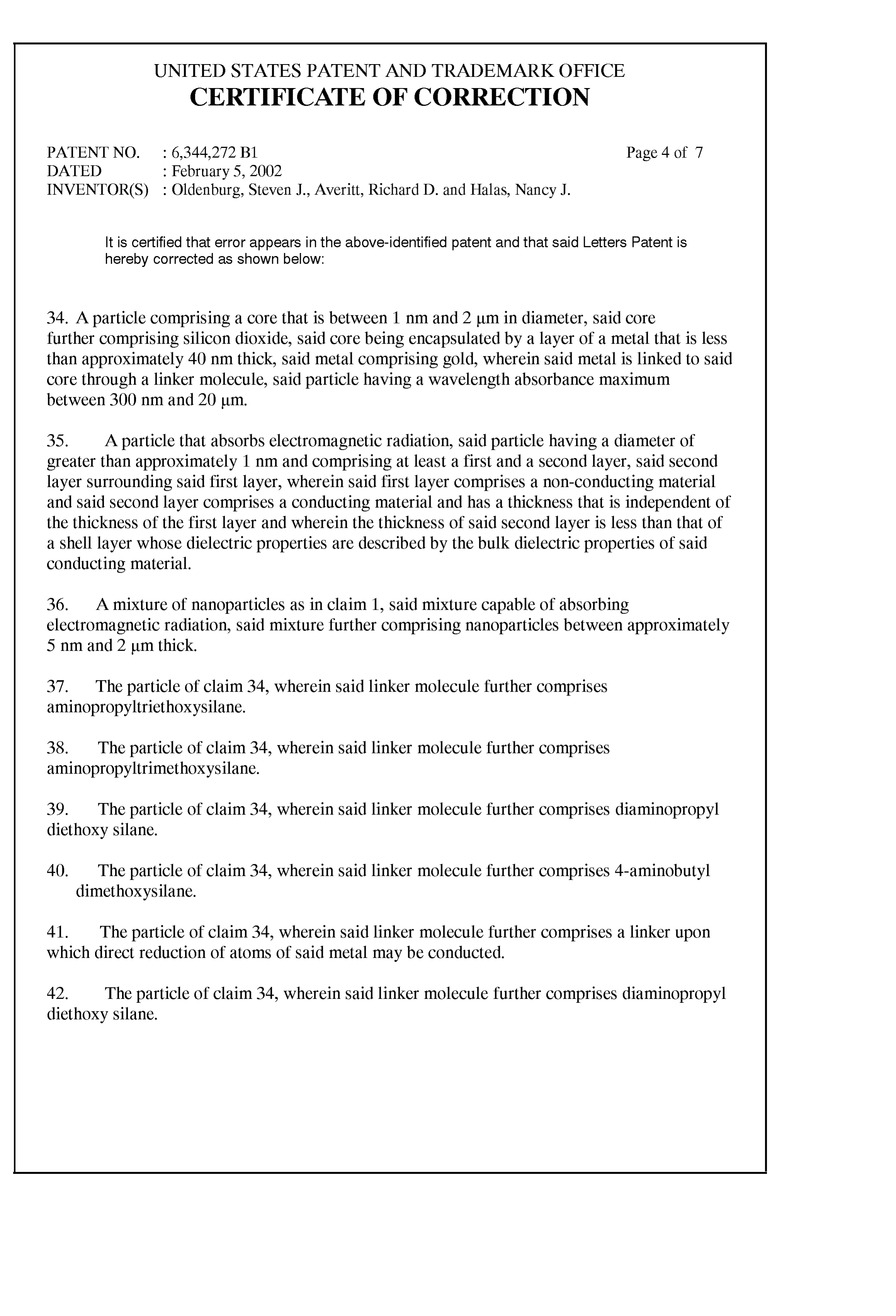
34. A particle comprising a core that is between 1 nm and 2 um in diameter, Said core further comprising Silicon dioxide, Said core being encapsulated by a layer of a metal that is leSS than approximately 40 nm thick, Said metal comprising gold, wherein Said metal is linked to Said core through a linker molecule, Said particle having a Wavelength absorbance maximum between 300 nm and 20 um.
35. A particle that absorbS electromagnetic radiation, Said particle having a diameter of greater than approximately 1 nm and comprising at least a first and a Second layer, Said Second layer Surrounding Said first layer, wherein Said first layer comprises a non-conducting material and Said Second layer comprises a conducting material and has a thickneSS that is independent of the thickness of the first layer and wherein the thickness of Said Second layer is less than that of a shell layer whose dielectric properties are described by the bulk dielectric properties of Said conducting material.
36. A mixture of nanoparticles as in claim 1, said mixture capable of absorbing electromagnetic radiation, Said mixture further comprising nanoparticles between approximately 5 nm and 2 um thick.
37. The particle of claim 34, wherein said linker molecule further comprises aminopropyltriethoxysilane.
38. The particle of claim 34, wherein said linker molecule further comprises aminopropyltrimethoxysilane.
39. The particle of claim 34, wherein said linker molecule further comprises diaminopropyl diethoxy silane.
40. The particle of claim 34, wherein said linker molecule further comprises 4-aminobutyl dimethoxysilane.
41. The particle of claim 34, wherein said linker molecule further comprises a linker upon which direct reduction of atoms of Said metal may be conducted.
42. The particle of claim 34, wherein said linker molecule further comprises diaminopropyl diethoxy silane.
Page 19
UNITED STATES PATENT AND TRADEMARK OFFICE
CERTIFICATE OF CORRECTION
PATENT NO. : 6,344,272 B1 Page 5 of 7
INVENTOR(S) : Oldenburg, Steven J., Averitt, Richard D. and Halas, Nancy J.
It is certified that error appears in the above-identified patent and that said Letters Patent is hereby corrected as shown below:
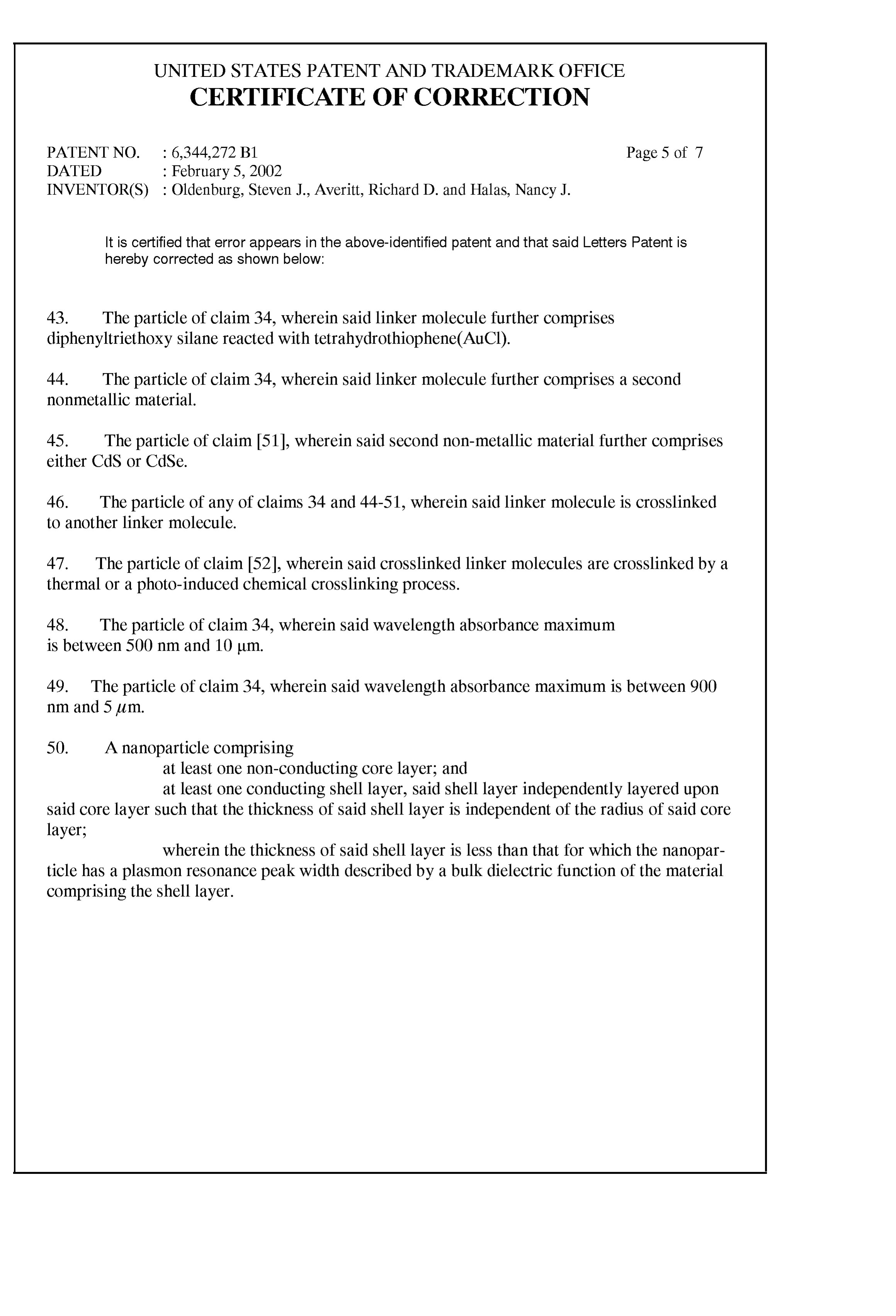
43. The particle of claim 34, wherein said linker molecule further comprises diphenyltriethoxysilane reacted with tetrahydrothiophene(AuCl).
44. The particle of claim 34, wherein said linker molecule further comprises a second nonmetallic material.
45. The particle of claim 51, wherein said Second non-metallic material further comprises either CdS or CdSe.
46. The particle of any of claims 34 and 44-51, wherein said linker molecule is crosslinked to another linker molecule.
47. The particle of claim 52, wherein said crosslinked linker molecules are crosslinked by a thermal or a photo-induced chemical croSSlinking process.
48. The particle of claim 34, wherein said wavelength absorbance maximum is between 500 nm and 10 um.
49. The particle of claim 34, wherein said wavelength absorbance maximum is between 900 nm and 5 lum.
50. A nanoparticle comprising at least one non-conducting core layer; and at least one conducting Shell layer, Said Shell layer independently layered upon said core layer Such that the thickness of Said shell layer is independent of the radius of Said core layer;
wherein the thickness of Said shell layer is less than that for which the nanopar ticle has a plasmon resonance peak width described by a bulk dielectric function of the material comprising the Shell layer.
Page 20
UNITED STATES PATENT AND TRADEMARK OFFICE
CERTIFICATE OF CORRECTION
PATENT NO. : 6,344,272 B1 Page 6 of 7
INVENTOR(S) : Oldenburg, Steven J., Averitt, Richard D. and Halas, Nancy J.
It is certified that error appears in the above-identified patent and that said Letters Patent is hereby corrected as shown below:
51. A nanoparticle comprising:
at least one non-conducting core layer; and at least one conducting Shell layer, Said Shell layer independently layered upon said core layer Such that the thickness of Said shell layer is independent of the radius of Said core layer;
wherein the thickness of Said shell layer is less than that of a shell layer for which the nanoparticle has a plasmon resonance peak width that is independent of the thickness of the shell layer.
52. A particle, comprising:
a core or inner layer, comprising a non-conducting material; and a shell layered above said core or inner layer and having a shell thickness, said Shell comprising a conducting material;
wherein said shell thickness is less than the bulk electron mean free path of Said conducting material.
53. A particle comprising a core that is less than 1 micron in diameter, said core further com prising a dielectric material, Said core being encapsulated by a layer of a metal that is leSS than approximately 40 nm thick, Said metal is Selected from the group consisting of to gold, Silver, copper, platinum, palladium, lead, and iron, Said particle having a Wavelength absorbance maximum in the infrared.

Page 21
UNITED STATES PATENT AND TRADEMARK OFFICE
CERTIFICATE OF CORRECTION
PATENT NO. : 6,344,272 B1 Page 7 of 7
INVENTOR(S) : Oldenburg, Steven J., Averitt, Richard D. and Halas, Nancy J.
It is certified that error appears in the above-identified patent and that said Letters Patent is hereby corrected as shown below:
54. A particle comprising a core that is leSS than 1 micron in diameter, Said core further comprising a dielectric material, Said core being encapsulated by a layer of a metal that is leSS than approximately 40 nm thick, Said metal is Selected from the group consisting of to gold, Silver, copper, platinum, palladium, lead, and iron, Said particle having a Wavelength Scattering maximum in the infrared.
Signed and Sealed this
Tenth Day of September, 2002
Attest.
JAMES E ROGAN
Attesting Officer Director of the United States Patent and Trademark Office
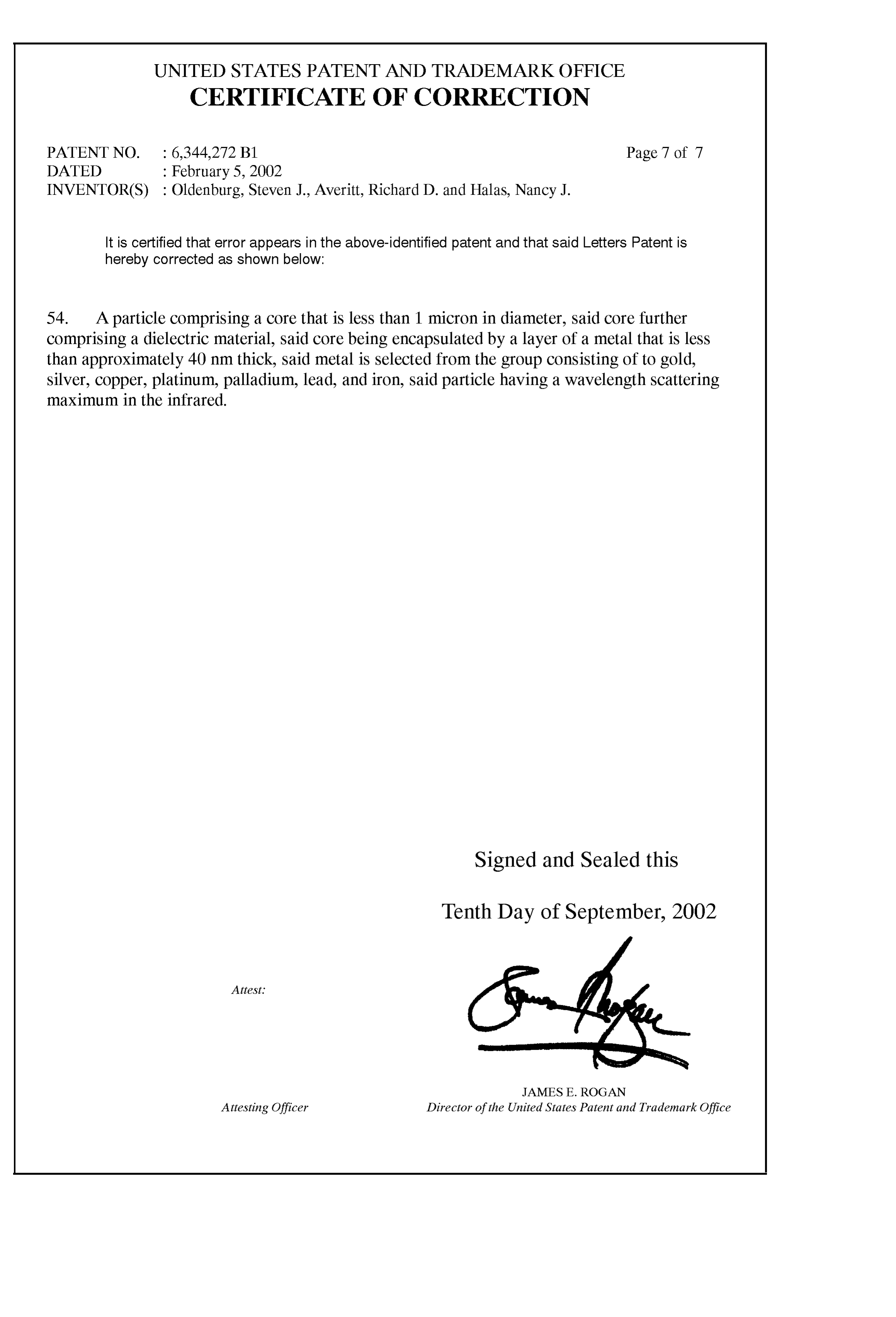
Page 22
UNITED STATES PATENT AND TRADEMARK OFFICE
CERTIFICATE OF CORRECTION
PATENT NO. : 6,344,272 B1 Page 1 of 1
INVENTOR(S) : Steven J. Oldenburg et al.
It is certified that error appears in the above-identified patent and that said Letters Patent is hereby corrected as shown below:
Column 1, Lines 17-19, replace The research that resulted in this invention was funded by the Office of Naval Research, N00014-97-1-0217, and the National Science Foundation, ECS-92581 18. with -- This invention was made with government support under Grant Number N00014-97-1-0217 awarded by the Office of Naval Research, and Grant Number ECS-92581 18 awarded by the National Science Foundation. The government has certain rights in the invention. --
Signed and Sealed this
Twenty-ninth Day of June, 2010
David J. Kappos
Director of the United States Patent and Trademark Office
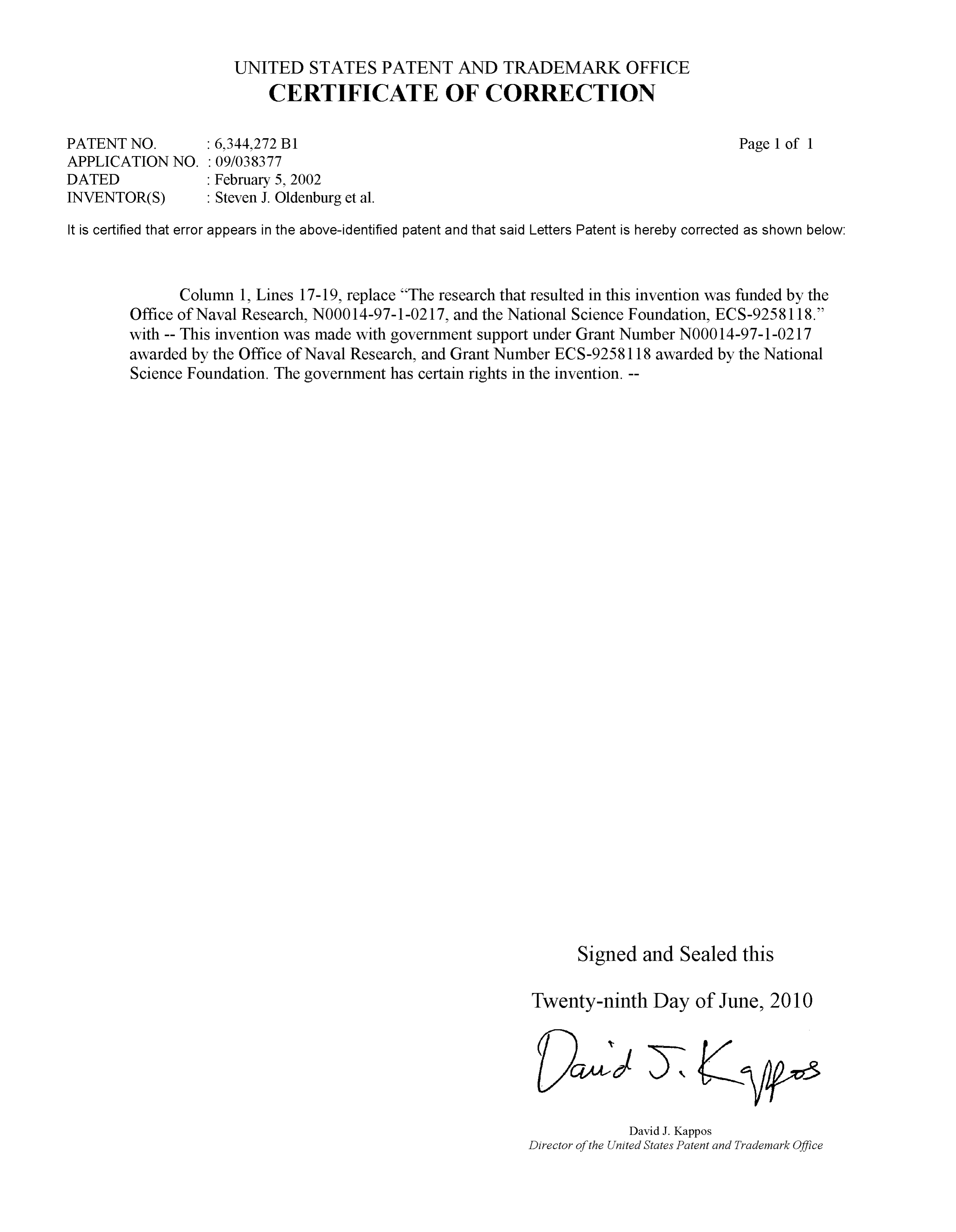
Provenance
- Collection
- Cited prior art
- Original PDF
- patentimages.storage.googleapis.com →
- Filed
- 1998-03-11
- Pages
- 22
- Method
- pdftotext (the PDF's own text layer) + pdftoppm 300dpi page scans
- Source
- Google Patents bibliographic record
- Granted
- 2002-02-05
- Inventors
- Steven J. Oldenburg; Richard D. Averitt; Nancy J. Halas; William Marsh Rice University
- Transcribed from
- patentimages.storage.googleapis.com →