patent · US5311009
Quantum well device for producing localized electron states for detectors and modulators
10 May 1994
Page 1 — bibliographic record
United States Patent (19) 11 Patent Number: 5,311,009 Capasso et al. 45 Date of Patent: May 10, 1994 (54) QUANTUM WELL DEVICE FOR quantum barrier", Appl. Phys. Lett, vol. 56, pp. 871-873 PRODUCING LOCALIZED ELECTRON (1990). Feb. 26, 1990.
STATES FOR DETECTORS AND J. Salzman, et al. "Bragg confinement of carriers in a MODULATORS shallow quantum well', Appl. Phys. Lett, vol. 59, pp. 75) Inventors: Federico Capasso, Westfield; Alfred 1858-1860 (1991). Jul. 15, 1991. Y. Cho, Summit; Jerome Faist, K. Iga, et al., "Electron Reflectance of Multiquantum Scotch Plains; Carlo Sirtori, Summit; Barrier (MQB)', Electronics Letters, vol. 22, No. 19, pp. Deborah L. Siveo, Warren, all of N.J. 1008-1010 (1986). Sep. 11, 1986.
73) Assignee: AT&T Bell Laboratories, Murray R. Dingle, et al. "Quantum States of Confined Carriers Hill, N.J. in Very Thin AlGa1-xAs-GaAs-AlGa1-xAs Heteros tructures', Physical Review Letters, vol. 33, No. 14, pp.
(21) Appl. No.: 923, 197 827-830 (1974) Sep. 30, 1974. - (22) Filed: Jul. 31, 1992 L. Esaki, et al. "New Transport Phenomenon in a Semi conductor 'Superlattice", Physical Review Letters, 51) Int, C. ............................................. H01L 27/12 vol. 33, No. 8, pp. 495-498 (1974) Aug. 19, 1974. 52 U.S.C. ................................ 250/214 LS; 257/17; (List continued on next page.)
58) Field of Search .................. 250/214.1, 338.4, 339, 250/370.01, 370.08, 370.12, 214.65; 257/14, 15, Primary Examiner-David C. Nelms
(56) References Cited Attorney, Agent, or Firm-Glen E. Books
4,894,526 1/1990 Bethea et al. .................... 250/214.1 In accordance with the invention, a quantum well de 5,023,685 6/1991 Bethea et al. ......................... 357/30 vice provides localized states for electrons having an 5,036,371 7/1991 Schwartz .............................. 257/14 energy E greater than the barrier height of the constitu 5,068,867 11/1991 Hasenberg et al................ 257/17 X ent quantum wells. The device comprises a confinement 5,091,756 2/1992 Iga et al. ................................. 357/4 quantum well of width Lwequal to an integer number n 5,105,301 4/1992 Campi ............... 257/17 X of deBroglie half wavelengths
5,142,341 8/1992 Goronkin et al. ... 257/87 X 5,185,647 2/1993 Vasquez ... ... 257/17 Lw - n 5,187,553 2/1993 Makita ................................. 257/187 and a plurality of adjacent quarter wavelength barriers
OTHER PUBLICATIONS and wells, each having a thickness equal to an odd num K. Kishino, et al. "Enhanced carrier confinement effect ber m of deBroglie quarter wavelengths. Constructive by the multiquantum barrier in 660 nm GalnP/AllnP interference between the waves partially reflected by visible Lasers', Appl. Phys. Lett, vol. 58, pp. 1822-1824 the interfaces between adjacent A/4 barriers and A/4 (1991). Jan. 31, 1991. wells leads to the formation of a localized electron state T. Takagi, et al. "Electron-wave reflection by multi at an energy E in the region of the confinement well. -quantum barrier in n-GaAs/i-AlGaAs/n-GaAs tun The device can be used in detectors and modulators neling diode", Appl. Phys. Lett., vol. 59, pp. 2877-2879 employing transitions between a bound state within the (1991). Sep. 4, 1991. well and the localized state above the well. T. Takagi, et al. "Design and Photoluminescence Study on a Multiquantum Barrier", IEEE.J. of Quantum Elec
G. Lenzi, et al. "Bragg confinement of carriers in a 8 Claims, 4 Drawing Sheets
Page 2
OTHER PUBLICATIONS AlGainP Multi-Quantum Barrier (MQB)', Japanese Journal of Applied Physics, vol. 29, No. 11, pp.
F. H. Stillinger, et al. "Bound states in the continuum', L1977-L1980 (1990) Nov. 11, 1990. Physical Review A, vol. 11, No. 2, pp. 446-454 (1975). J. Weidmann, “Zur Spektraltheorie von Sturm-Li Feb. 1975. ouville-Operatoren' Math, Zeitschr, vol. 98, pp. D. R. Herrick, "Construction of Bound States in the 268-302 (1967).
Continuum for Epitaxial Heterostructure Superlat F. H. Stillinger, et al. "Role of electron correlation in tices', Physica, vol. 85B, pp. 44-50 (1977). determining the binding limit for two-electron atoms', F. H. Stillinger, "Potentials Supporting Positive-En Physical Review A, vol. 10, No. 4, pp. 1122-1130 (1974). ergy Eigenstates and Their Application to Semiconduc Oct. 1974.
tor Heterostructures', Physica, vol. 85B, pp. 170-276 B. Simon, "On Positive Eigenvalues of One-Body (1977). Schrodinger Operators', Conn, on Pure and Applied T. Takagi, et al. "Potential Barrier Height Analysis of Math., vol. XXII, pp. 531-538 (1967).
Page 3
Drawing sheet — no readable text.
Page 4
Drawing sheet — no readable text.
Page 5
Drawing sheet — no readable text.
Page 6
Drawing sheet — no readable text.
Page 7
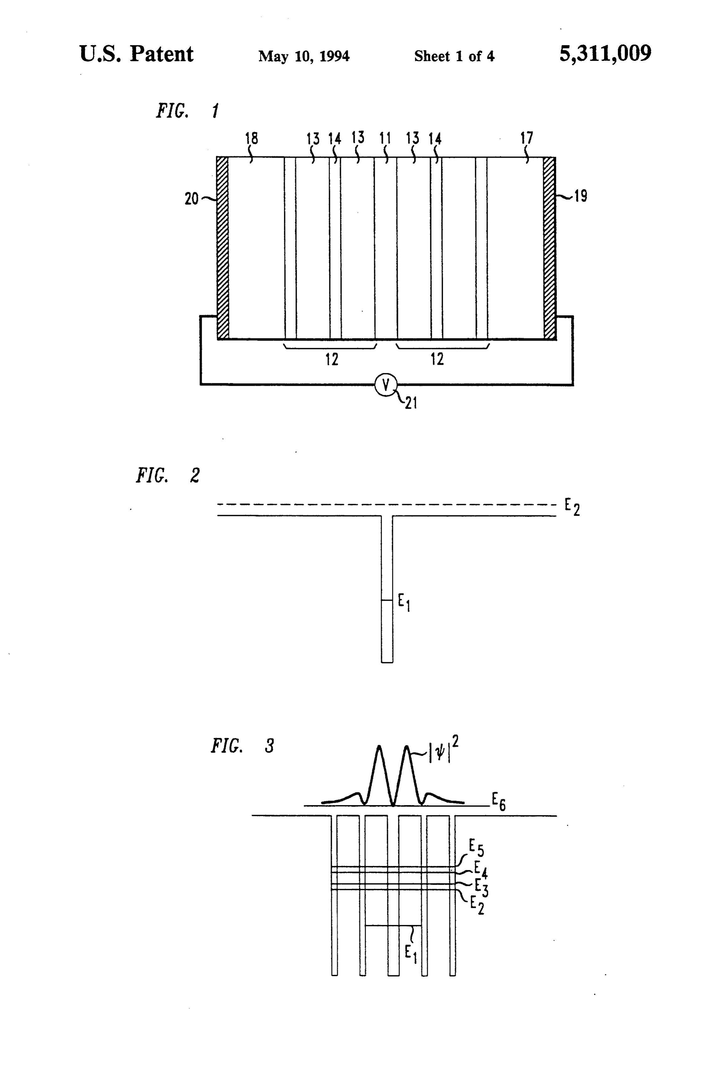
FIG.3, which is also conceptual, shows energy levels
QUANTUM, WELL DEVICE FOR PRODUCING and a wave function for an idealized device according LOCALIZED ELECTRON STATES FOR to FIG. 1,
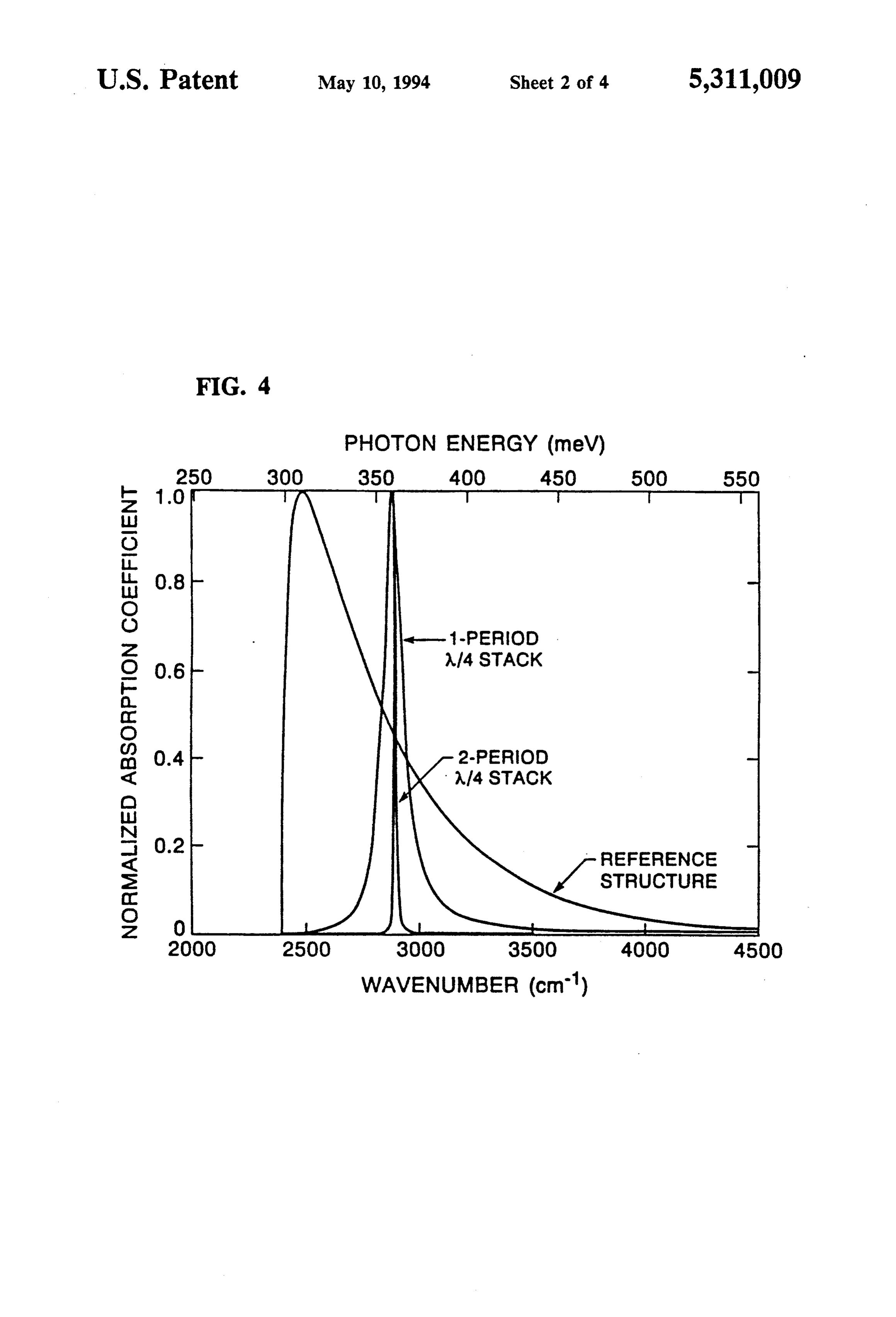
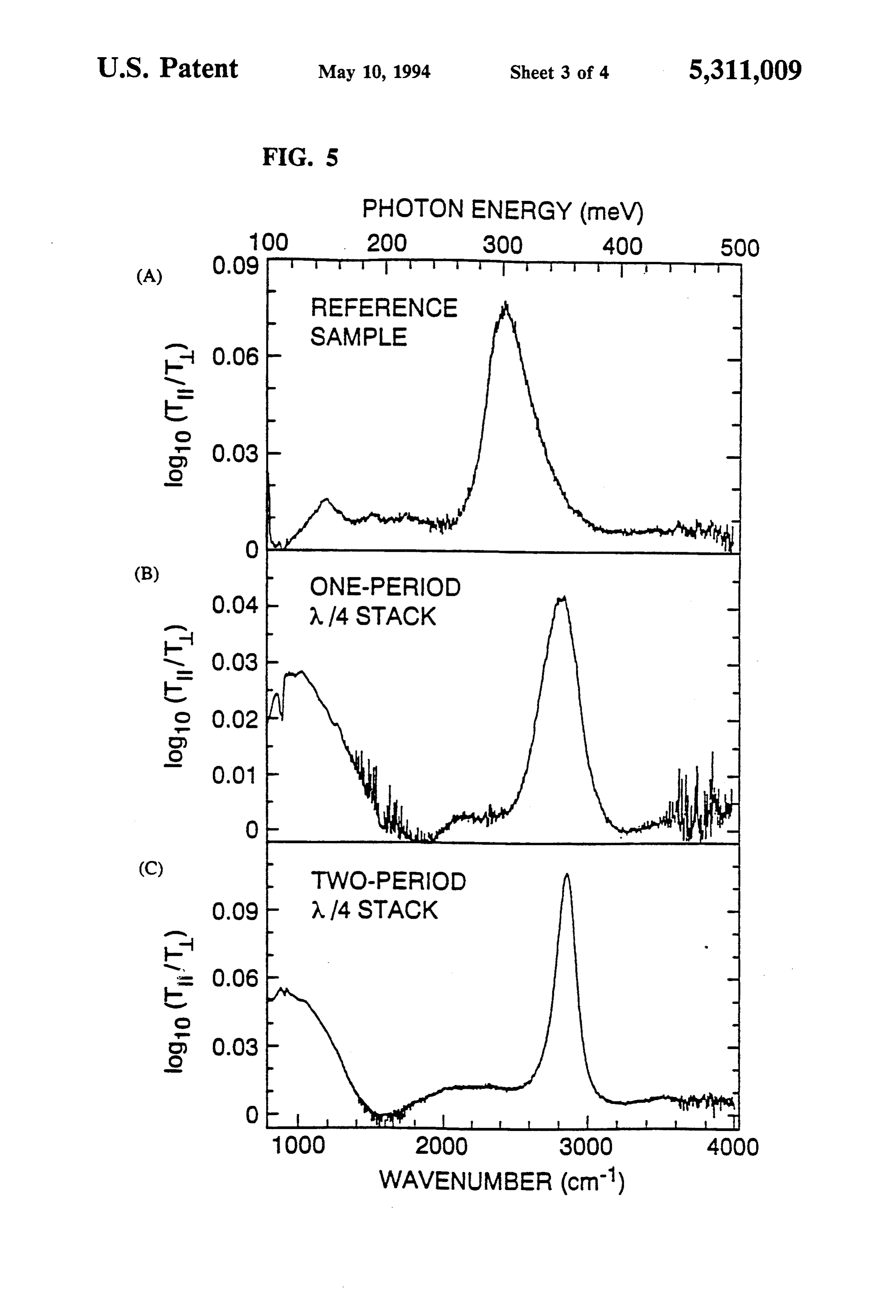
DETECTORS AND MODULATORS FIG. 4 is a graphical illustration showing predicted FIELD OF THE INVENTION absorption spectra for a constructed reference structure and constructed devices of the type shown in FIG. 1;
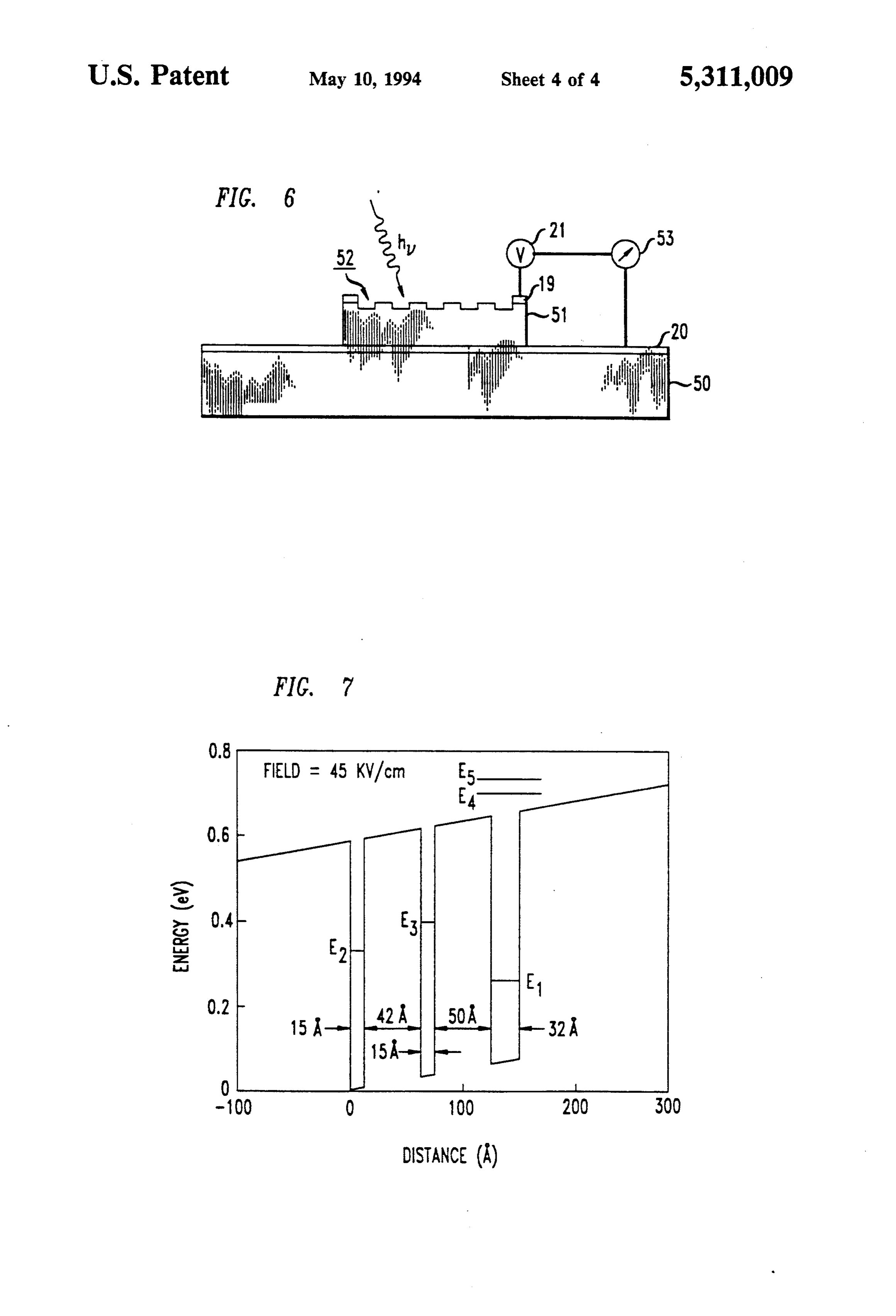
This invention relates to quantum well devices and, in FIG. 5a-c are graphical illustrations showing the particular, to a quantum well device capable of produc measured absorption for constructed devices; ing localized states for electrons having energy greater O FIG. 6 is a schematic cross section of a photodetector than the barrier height. The device is particularly useful using a FIG. 1 device; and in detectors and modulators. FIG. 7 is an energy level diagram of a modified de BACKGROUND OF THE INVENTION vice which can be used as either a photodetector or an optical modulator.
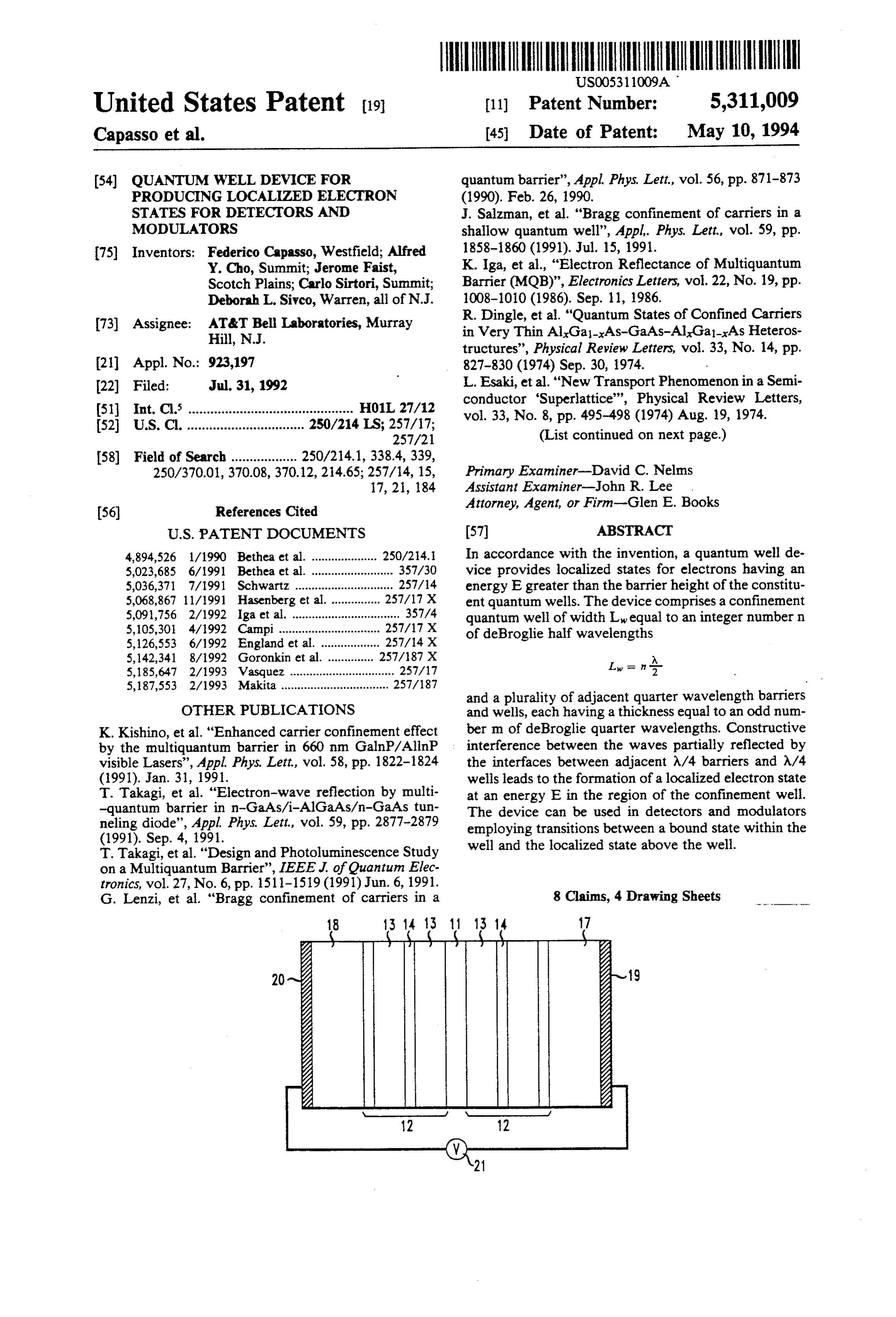
It is known that quantum well devices can bind elec 15 It is to be understood that these drawings are for trons having energy less than the barrier heights of the purposes of illustrating the concepts of the invention constituent wells. Indeed such devices have been en ployed as infrared photodetectors. For example. U.S. and, except for graphical data, are not to scale. Pat. No. 4,894,526 issued Jan. 16, 1990, to Bethea et al., DETAILED DESCRIPTION discloses a detector wherein infrared radiation incident 20 on a superlattice of doped quantum wells gives rise to Referring to the drawings, FIG. 1 is a schematic cross intersubband resonance radiation which excites elec section of a quantum well device which can effectively trons from the ground state in a well into an excited localize electrons of energy E greater than the barrier state. A photocurrent results from excited electrons height of the quantum well. In essence, the device 10 tunneling out of the quantum wells. U.S. Pat. No. 25 comprises a sequence of epitaxial heterolayers-barrier 5,023,685, issued Jun. 11, 1991, to Bethea et al., also layers and well layers-forming confinement quantum shows a quantum well radiation detector. The wells well 11 of thickness have but a single-bound energy state.
The present applicant has discovered that, in addition in A to having electron bound states within a quantum well 30 2. ' at energies below the barrier height, devices can be fabricated which have localized electron states at ener where A is the deBroglie wavelength for an electron of gies above the barrier height. This discovery permits energy E and n is an integer. Adjacent well 11, on one the fabrication of a variety of new detectors and modu or both sides, are quarter wave stacks 12 of barriers 13 lators. 35 and wells 14 each having thicknesses of
SUMMARY OF THE INVENTION
In accordance with the invention, a quantum well m 4.- device provides localized states for electrons having an energy E greater than the barrier height of the constitu where m is an odd integer. The electron energy E can ent quantum wells. The device comprises a confinement be higher than the barrier height of the confinement quantum well of width Lwequal to an integer number n well 11. The device can comprise a single repetition of of deBroglie half wavelengths a confinement well and quarter wave stacks or it can 45 comprise many repetitions of the confinement well
L = n :- quarter wave stack structure. Advantageously, contact layers 17 and 18 are provided for permitting ohmic and a plurality of adjacent quarter wavelength barriers contacts 19 and 20, and a voltage source 21 permits the and wells, each having a thickness equal to an odd num application of a voltage V across the device. ber m of deBroglie quarter wavelengths. Constructive SO It should be understood that the thickness of the A/4 interference between the waves partially reflected by barriers 13 will be different than the thickness of the A/4 the interfaces between adjacent A/4 barriers and A/4 wells 14. This difference is because an electron of en wells leads to the formation of a localized electron state ergy E measured from the botton of the well has a at an energy E in the region of the confinement well. different deBroglie wavelength in the barrier layer than The device can be used in detectors and modulators 55 has in the well layer. If E is the electron energy mea employing transitions between a bound state within the itsured from the botton of a well and AE is the barrier well and the localized state above the well.
height, then E=E-AE is the energy for calculating
BRIEF DESCRIPTION OF THE DRAWINGS the wavelength in a barrier region. Specifically, the The advantages, nature and various additional fea deBroglie wavelength is A=27t/K where K is the wave tures of the invention will appear more fully upon con number. In a well region the wave number is sideration of the illustrative embodiments now to be described in detail in connection with the accompany ing drawings. In the drawings: Kw -
FIG. 1 is a schematic cross section of a quantum well 65 device with a localized state at energy above the well;
FIG. 2, which is conceptual, shows energy levels for where n is the effective electron mass in the well. In an idealized rectangular model quantum well; a barrier region the wave number is
Page 8
ples had 32 A. In GaAs quantum wells n-doped to the same level, and the quarter wave stacks comprised 1, 2 and 6 periods, respectively, each period comprising an
undoped 39 A AlInAs barrier and an undoped 16 A
GainAs well. A plurality of such devices separated by where m is the effective electron mass. The thickness undoped 150 A AllnAs layers were grown on each of the confinement well Lw satisfies the condition substrate. On each substrate the growth started and KL=nar, where n is an integer. The A/4 wells satisfy terminated with n-type GainAs contact layers. 10 Theoretical absorption spectra were calculated for the reference sample and for the devices with 1 and 2
K.L. = m , period quarter wave stacks. FIG. 4 is a plot of the pre dicted absorption coefficients as functions of wave nun where m is odd and the A/4 barriers satisfy ber. As can be seen, substantial narrowing of the absorp 5 tion peak is produced by one or two period stacks.
Tests demonstrated that the quarter-wave stack
Kbb = n f structures behave as a good approximation of a state highly localized above the confinement well. The sam
In operation, the device exhibits electron localization ples were processed into six-pass 45' edge waveguides, at the confinement well for electrons of energy E, local and the absorption spectra were measured with a Nico izing such electrons in the well even though E is above let System 800 Fourier transform infrared spectrometer. the barrier height. This operation can be understood by FIGS. 5A, 5B, and 5C show the measured spectra for reference to FIGS. 2 and 3. FIG. 2 schematically shows the reference, the 1 period and the 2 period devices, the energy levels for a conventional rectangular quan respectively. As can be seen, the absorption peak corre tum well. As shown, there can be bound states of elec 25 sponding to transitions to states above the well is much trons having kinetic energy E1 less than the barrier narrower in the 2 period quarter-wave reflector struc height. However for electrons of energy E2 greater than ture than in the reference sample. The position of the the barrier height there is a continuum of scattering absorption peak shifts to higher energy in the samples states producing extended electron wave functions with with quarter-wave stacks, and the width of the absorp non-vanishing amplitudes at infinity. There are trans 30 tion peak narrows by nearly a factor of two in going mission resonances (not shown) for discrete energies corresponding to a semi-integer number of electron from the 1 period to the 2 period structure. FIG. 6 is a schematic cross section of a photodetector wavelengths across the well. At these discrete energies the electron wave amplitude is enhanced, but the corre using a device of the type shown in FIG. 1. The struc sponding states remain extended. The wave functions 35 ture comprises in essence, a semi-insulating substrate 50, do not decay exponentially in the barriers, but rather a quantum well device 51 comprising a plurality of extend in a manner similar to plane waves. The elec repetitions (preferably 20-50) of the confinement well trons are not bound. -(A/4) stack structure, means for coupling light (hu) FIG. 3 schematically illustrates the energy levels and into the device 51 such as a grating 52, and a current an associated electron wave function for the device of 40 measuring instrument 53 serially connected with the FIG. 1. The individual quantum wells can have bound voltage source of the device 51.
states E1 through Es, but in addition, the structure of When used as a photodetector, the device is prefera FIG. 1 can sharply localize the resonance states. The bly constructed so that the confinement wells have a waves reflected from interfaces in the stacks 12 con single bound state E1 within the well and a localized structively interfere leading to a localized concentration 45 state E4 above the well, such that E4-El=hu for the of probability density 112 in the region of the confine light to be detected. By suitable choice of the materials ment well 11. Thus a localized electron state at energy and layer thicknesses the response wavelength can be E6 is produced in the region of well 11. In the limit of a superlattice of A/4 stacks, the stacks become ideal tuned from the near infrared (~1 um) to the far infrared Bragg reflectors, and the localized state approaches a 50 A) dopedm).confinement (10–70 For example, a structure with GanAs (30 wells and true bound state. Experiments show that the presence of one or more quarter wave pairs considerably enhances the degree of localization.
The fabrication and structure of the invention can be
understood in greater detail by consideration of the 55 following specific examples. The exemplary structures stacks has a narrow photoresponse centered at 3.54 micrometers. In operation a small bias of 1-30 kV/cm is can be conveniently fabricated by using molecular bean applied to collect epitaxy (MBE) to grow the layers for the confinement ing instrument 53photocurrent, provides a and the current measur measure of the incident well 11, A/4 barriers 13 and A/4 wells 14.
Four types of structures were fabricated: a reference light at 3.54 micrometers wavelength. sample consisting of quantum wells bound by conven As a second example, a narrow band photodetector tional thick barriers and device samples with similar for 11 pum radiation can be made by a similar structure quantum wells clad by quarter-wave stacks consisting using a quantum well device with 38 A GaAs confine of 1, 2 and 6 periods (barrier-well pairs). The reference ment wells and quarter wave Alo.22Gao.78As(80 sample was grown by MBE lattice matched to insulat 65 A)/GaAs (19 A) stacks.
A third example, shown in FIG. 7, employs quarter ing (100). InP substrates. The reference had twenty 32A
InGaAs quantum wells n-doped to 1x101 cm-3, all wave stacks on but one side of the confinement well. Such a device can comprise a separated by 150 A AlInAs barriers. The device sam
Page 9
thickness L equal to an integral number n of half
deBroglie wavelengths of an electron of energy E;
adjacent said well layer on at least one side thereof a quarter wave stack of barrier layers and well lay well n-doped to 1018 cm-3 having a quarter wave All ers;
nAs/GanAs stack on only one side. The stack is di said stack barrier layers having a thickness Libequal to mensioned as shown in FIG. 7 to account for the varia an odd number of quarter deBroglie wavelengths tion in deBroglie wavelength produced by the voltage of an electron of energy E; and bias. At zero or small bias the absorption spectrum of O said stack well layers having a thickness Ls equal to the device is broad because the electron state is ex an odd number of quarter deBroglie wavelength of tended. But when a 45 kV/cm bias is applied, a local an electron of energy E. ized state is formed, with electrons confined on one side 2. A device according to claim 1 comprising quarter by the quarter wave stack and on the other by the rising wave stacks on both sides of said confinement quantum well barrier. With bias, the photon absorption is now 15 well. 3. A device according to claim 1 wherein said con narrow band and peaked at photon energy fia)=E.-E. finement
The device can thus be used as a photodetector for 3.5 tron statequantum
well includes at least one bound elec energy E1 within the well.
um radiation. Alternatively, variation of the bias volt 4. A device according to claim 3 further comprising age as by a pulsed voltage supply (not shown) permits means for directing into said device photons of radia the device to be used as an optical modulator. If mono 20 tion having energy equal to E-E1. chromatic light at the peak frequency is input to the 5. A device according to claim 1 including means for device, variation of the bias voltage will vary the applying voltage across said device.
amount of light absorbed. 6. A photodetector comprising a device according to It is to be understood that the above-described en claim 4 for absorbing photons of radiation having en bodiments are illustrative of only a few of the many 25 ergy equal to E-El and means for measuring the cur possible specific embodiments which can represent ap rent generated by such absorption.
plications of the principles of the invention. Thus, nu 7. An optical modulator comprising a device accord merous and varied other arrangements can be made by ing to claim 4 for absorbing photons of radiation having those skilled in the art without departing from the spirit energy equal to E-E1 and means for varying the and scope of the invention. amount of light absorbed by said device. We claim: 8. The modulator of claim 7 wherein said device 1. A quantum well device for providing a localized according to claim 4 comprises a device having a quar state for electrons of energy E measured from the bot ter wave stack on only one side of said confinement well tom of the well greater than the barrier height AE of and said means for varying the light absorbed by said the adjacent barrier layers comprising: 35 device comprises means for varying a bias voltage ap a confinement quantum well layer disposed between plied to said device. k s sk k k a pair of barrier layers, said well layer having a
Provenance
- Collection
- Cited prior art
- Original PDF
- patentimages.storage.googleapis.com →
- Filed
- 1992-07-31
- Pages
- 9
- Method
- pdftotext (the PDF's own text layer) + pdftoppm 300dpi page scans
- Source
- Google Patents bibliographic record
- Granted
- 1994-05-10
- Inventors
- Federico Capasso; Alfred Y. Cho; Jerome Faist; Carlo Sirtori; Deborah L. Sivco; AT&T Bell Laboratories Inc
- Transcribed from
- patentimages.storage.googleapis.com →