patent · US5124610
Tritiated light emitting polymer electrical energy source
23 June 1992
Page 1 — bibliographic record
United States Patent (19) 11) Patent Number: 5,124,610 Conley et al. (45) Date of Patent: Jun. 23, 1992 (54) TRITIATED LIGHT EMITTING POLYMER Foldiak, G., Industrial Applications Radio Isotopes, 1986 ELECTRICAL ENERGY SOURCE p. 387.
75) Inventors: Jerry J. Conley; Gary B. Mortensen, Yang, Fundamentals of Semiconductor Devices, 1978, pp.
both of Waseca, Minn.
"Power Sources for Space Explored', Aviation Week, 73) Assignee: E. F. Johnson Company, Waseca, vol. 68, Jun. 16, 1958; pp. 235, 7, 9 and 241. Minn. D. A. Sukhov & F. I. Vilesov, "Photoionization of (21) Appl. No.: 664,203 Aromatic Hydrocarbons Dissolved in Polymethyl Methacrylate and Polystyrene', Proc. IRC, vol. 4, No.
(22 Filed: Mar. 4, 1991 8; pp. 134-136.
Related U.S. Application Data Primary Examiner-Nelson Moskowitz 63) Continuation-in-part of Ser. No. 347,155, May 3, 1989, Attorney, Agent, or Firm-Patterson & Keough abandoned, which is a continuation-in-part of Ser. No. (57) ABSTRACT
An electrical energy source is created by the combina 51) int. Cl. ........................ G21H 1/00; G21H 1/12; tion of a light emitting polymer material having at least G21D 7/00; CO2F 112/12 one light emitting surface emitting light energy of a 52 U.S. Cl. .................................... 310/303; 310/302; specified frequency bandwidth and a photovoltaic cell 136/249; 313/504 having a light collecting surface and a pair of electrical (58) Field of Search ................ 310/302, 303; 136/249, contacts. The light collecting surface of the photovol 136/253; 357/30, 313/504 taic cell is optically coupled with the light emitting 56) References Cited surface of the light emitting polymer material. An open
circuit voltage is generated between the pair of electri cal contacts as a result of the absorption of emitted light 2,259,372 10/1941 Geisler . energy from the light emitting polymer material by the 2,847,585 8/1958 Christian ............................. 310/303 photovoltaic cell. The light emitting polymer comprises 3,031,519 4/1962 Silverman, a mixture of a polymer labelled with a tritium and an 3,033,797 5/1962 DeLeo et al. .................... 252/301.1 organic compound which emits light energy when sub 3,053,927 9/1962 Viszlocky . jected to radiation generated by the tritium. The or 3,094,634 6/1963 Rappaport .......................... 310/303 ganic compound is at least partly bonded to the polymer (List continued on next page.) and the mixture is translucent at the specified frequency bandwidth of the light energy. Maximum absorption of
FOREIGN PATENT DOCUMENTS the emitted light energy is achieved by the intimate 615938 3/1961 Canada . optical contact between the light emitting surface and 204167 12/1986 European Pat. Off. . the light collecting surface, by matching the maximum 116324 6/1899 Fed. Rep. of Germany . absorption frequency bandwidth of the photovoltaic 073393 6/1976 Japan. cell with the specified frequency bandwidth of the emit 638106 5/950 United Kingdom . ted light energy from the light emitting polymer mate OTHER PUBLICATIONS rial, and by the structural arrangement of the light emit ting polymer material itself.
Van der Ziel, A., Solid State Physical Electronics, 1957 p.
390. 20 Claims, 6 Drawing Sheets
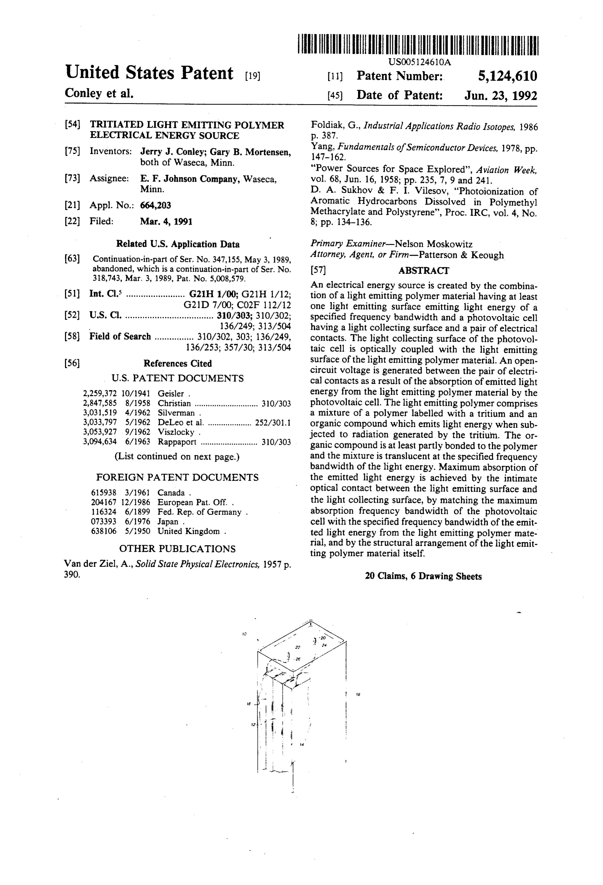
Page 2
3,304,445 2/1967 Weddell et al. . 4,242,47 12/1980 DeToia ............................... 310/303 3,325,420 6/1967 Futterknecht . 4,374,749 2/1983 Cusano et al. .
3,342,743 9/1967 Rosenberg. ... 252A30. 4,375,423 3/1983 Cusano et al. .
3,483,040 12/1969 Parkins .................................. 136/89 4,628,43 12/1986 Brotz .................................. 136/253 3,740,273 6/1973 Adler et al. 36/202 4,677,008 6/1987 Webb .
3,767,947 10/1973 Adler et al. ........................... 30/30 4,728,878 3/1988 Anthony .
3,939,366 2/1976 Ato et al. . 4,835,433 5/1989 Brown .
4,020,003 4/1977 Steinberg et al. . 4,889,660 2/1989 Jensen et al. ........................ 252/646

Page 3
Drawing sheet — no readable text.
Page 4
Drawing sheet — no readable text.
Page 5
Drawing sheet — no readable text.
Page 6
Drawing sheet — no readable text.
Page 7
Drawing sheet — no readable text.
Page 8
Drawing sheet — no readable text.
Page 9
for limited commercial activities. These low limits on
TRITIATED ELIGHT EMITTING POLYMER radioactive material effectively limit the radiation en ELECTRICAL ENERGY SOURCE ergy, and hence, the electrical energy that may be gen erated from any such source.
This application is a continuation-in-part of co-pend Using the amount of radioactivity as measured in ing application Ser. No. 347,155, filed May 3, 1989, now curies, the total amount of power available from such an abandoned which was a continuation-in-part of applica energy source can be calculated. Each curie of radioac tion Ser. No. 318,743, filed Mar. 3, 1989, now issued as tive material will produce 3.7 x 100 Beqerels (decays)- U.S. Pat. No. 5,008,579. /second. Assuming that the radioactive emission is in 10 the form of a beta particle from the radioisotope tritium
TECHNICAL FIELD
having an average 5.6 KeV of energy, the total theoreti
The present invention pertains to the generation of cal power emitted is 32.5 microwatts/curie. Theoreti electrical energy through the combination of a light cally, if there were a complete conversion of all of the source and a photovoltaic cell. In particular, this inven power of this nuclear radiation to electrical energy, the tion pertains to a long-life, electrical energy source 15 total amount of power available from a small, but safe, generated by the combination of a radioisotope acti amount of radioactive material containing less than 25 vated polymer material emitting a low level of light curies of tritium would be less than 1 milliwatt. Though with a photovoltaic cell arranged in intimate optical the total amount of power generated by such a device contact with the light emitting polymer material, the over the half life of the tritium radioactive material may light emitting polymer in the present invention being 20 be on the order of a hundred watt-hours, until recently comprised of a tritiated organic polymer to which an relatively few applications could operate with a contin organic phosphor or scintillant is bonded. uous power supply outputting in the microwatt range. BACKGROUND ART With the advent of CMOS and other low power cir cuitry, however, applications and uses for this type of
Various types of energy sources consisting of photo 25 long-life, low-watthour power supply are now becom cells activated by some type of nuclear radiation are ing more practical.
known in the prior art. These devices, somtimes re Although a variety of self-luminous, low light ferred to as "nuclear batteries' or "atomic batteries', sources have been available for a long time (e.g. radium convert nuclear electromagnetic radiation into electri and tritium activated phosphors used for creating self cal energy by one of two methods, single conversion 30 luminous paints for watch dials, etc., U.S. Pat. Nos. systems or double conversion systems. Single conver 3,033,797, 3,325,420 and 3,342,743), it has generally sion nuclear batteries generate electrical energy by been regarded that such materials were unsuitable for converting the nuclear radiation (i.e. alpha articles, beta commercial use for the conversion of light into electric particles or gamma radiation) into electrical energy by ity. The low levels of radioactivity associated with such direct absorption of the nuclear radiation at the p-n 35 materials, though generally not harmful or dangerous, junction of a semiconductor material, for example, U.S. do not provide an adequate source of power for the Pat. Nos. 3,094,634 and 3,304,445. Double conversion nuclear batteries of the type known in the prior art. In nuclear batteries generate electrical energy by convert addition to the low light level (50 micro-lamberts or ing the nuclear radiation into electromagnetic radiation, less), such sources may also be characterized by rapid usually by irradiating a phosphorescent material that and unpredictable light decay and, in the case of radi will generate light in the visible spectrum, and then um-activated light sources, may produce undesirable converting that electromagnetic radiation into electri radiation hazards associated with their decay products. cal energy by absorption of the electromagnetic radia Though the concept of a long-life, electrical energy tion at the p-n junction of a semiconductor material, source activated by a radioactive material is attractive usually a typical photovoltaic cell, for example, U.S. 45 and has many potential applications, none of the prior Pat. Nos. 3,031,519, 3,053,927, and 3,483,040. art devices have been able to create a safe, yet suffi While the concept of a nuclear battery is not new, a ciently powerful, energy source that is commercially practical and commercially feasible device of this type feasible. Accordingly, there is a continuing need to has not been possible because of the extreme dangers develop a safe and practical long-life, electrical energy involved in the handling and use of radioactive materi 50 source powered by a radioactive source. als. Most nuclear batteries of the type known in the SUMMARY OF THE INVENTION prior art have either been unsafe or have required such extensive shielding of the nuclear material used to In accordance with the present invention, an electri power the battery that the device is rendered impracti cal energy source is created by the combination of a cal for most applications. The regulatory standards for 55 light emitting polymer material having at least one light radiation leakage upon container failure impose addi emitting surface emitting light energy of a specified tional constraints that limit the applications for such frequency bandwidth and a photovoltaic cell having a devices. One possible means of overcoming these safety light collecting surface and a pair of electrical contacts. limitations is to limit the amount of radioactive material The light collecting surface of the photovoltaic cell is used in such a device. For example, in a typical smoke optically coupled with the light emitting surface of the detector a small amount of radioactive foil containing light emitting polymer material. An open-circuit volt one microcurie of radioactive Americium 241 is used to age is generated between the pair of electrical contacts power the detection circuit of the device. In general, as a result of the absorption of emitted light energy from regulatory standards allow for small amounts of radio the light emitting polymer material by the photovoltaic active material to be used under certain circumstances. 65 cell.
For example, with proper shielding and packaging, a The light emitting polymer comprises a mixture of a device containing 5 curies of radioactive material may polymer labelled with a tritium and an organic com be approved by the Nuclear Regulatory Commission pound which emits light energy when subjected to
Page 10
radiation generated by the tritium. The organic com very constant source of power and ensure that it is not pound is at least partly bonded to the polymer and the drained of its energy if subjected to a short-circuit. mixture is translucent at the specified frequency band Moreover, the materials and packaging of the present width of the light energy. Maximum absorption of the invention can be selected to enable the electrical energy emitted light energy is achieved by the intimate optical source to operate in a cryogenic environment without contact between the light emitting surface and the light significant degradation of the power compared to con collecting surface, by matching the maximum absorp ventional chemical batteries, because the rate of conver tion frequency bandwidth of the photovoltaic cell with sion of the photons by the photovoltaic cell is positively the specified frequency bandwidth of the emitted light affected by decreasing temperature. energy from the light emitting polymer material, and by 10 Although light emitting polymers have been avail the structural arrangement of the light emitting polymer able for a number of years for various uses (primarily as material itself. To maximize the surface area between self-luminescent paints), it is not known to use such light the light emitting polymer and the photovoltaic cell, the emitting polymers to power electrical energy source light emitting surface and the light collecting surface The present invention has discovered their usefulness are preferably arranged so that they are generally paral 15 for this purpose and, more importantly, the adaptability lel to and in intimate contact with each other. In addi tion, the light emitting polymer material and the photo of light emitting polymers as compared to other prior voltaic cell may be arranged to allow the photovoltaic cal radioisotope art energy vehicles to permit the design of electri sources with greater efficiency and safety cell to be constructed in manner so as to absorb light than in prior art devices.
energy at more than a single surface. 20
Accordingly, a primary objective of the present in
In another embodiment of the present invention, the vention light emitting polymer material is optically separated long-life,is toradioisotope-powered provide a safe, yet sufficiently powerful, from the photovoltaic cell by an optical control means source that is commercially feasible.electrical energy for controlling the amount of light that may pass Another objective of the present invention is to pro through the optical control means to be absorbed by the 25 vide a long-life source of electrical energy by the com photovoltaic cell. The optical control means may be a bination liquid crystal display (LCD) or lead lantium zirconium mer and of a a radioisotope-activated, light emitting poly photovoltaic cell.
titinate (PZLT) or similar material that is either trans A further objective of the present invention is to parent or opaque, depending upon the voltage or cur rent applied to the material. By controlling the amount 30 provide an electrical energy source wherein the conver of light that may be absorbed by the photovoltaic cell, sion efficiency by a photovoltaic cell of light emitted by the optical control means also controls the output of the a light emitting polymer is maximized. photovoltaic cell and, hence, operates as either a volt An additional objective of the present invention is to age or current regulator, depending upon the particular provide an electrical energy source that includes an circuit that utilizes the electrical energy source of the 35 optical control means for controlling the amount of present invention. The optical control means allows the electrical energy generated by controlling the amount electrical energy source of the present invention to of light that is received by the photovoltaic cell from a simulate an alternating current source from a direct light source.
current source without the need for electrical circuitry A still further objective of the present invention is to external to the electrical energy source. provide a long-life, electrical energy source that pro The present invention provides a novel radioisotope vides a consistent power output by generating electrical activated, electrical energy source that exhibits several energy at a constant watt-hour rate. desirable characteristics. Forenost, the electrical en These and other objectives of the present invention ergy source of the present invention is relatively safe will become apparent with reference to the drawings, and is, thus, viable for general commercial use when the 45 the detailed description of the preferred embodiment quantities of radioactivity are generally below 100 cu and the appended claims.
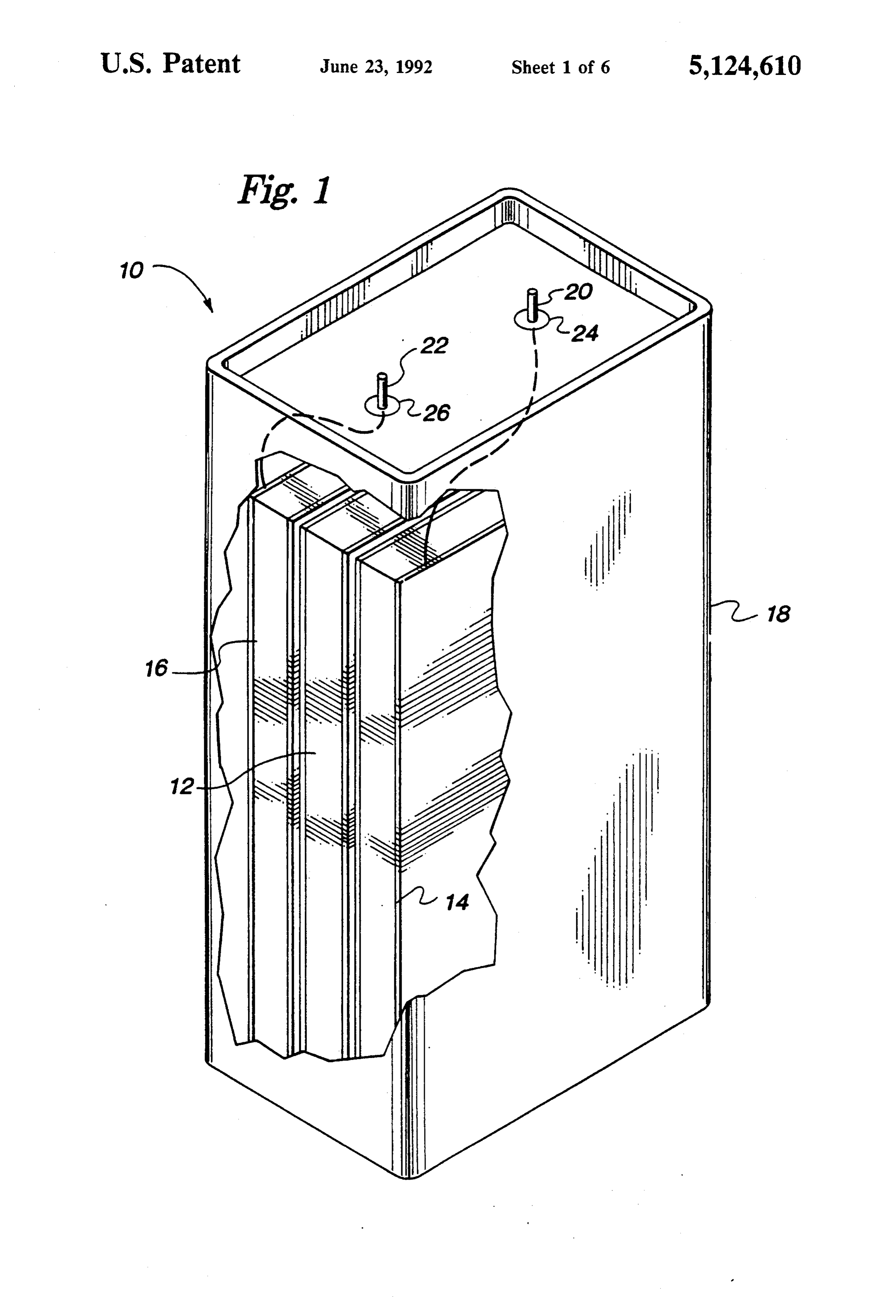
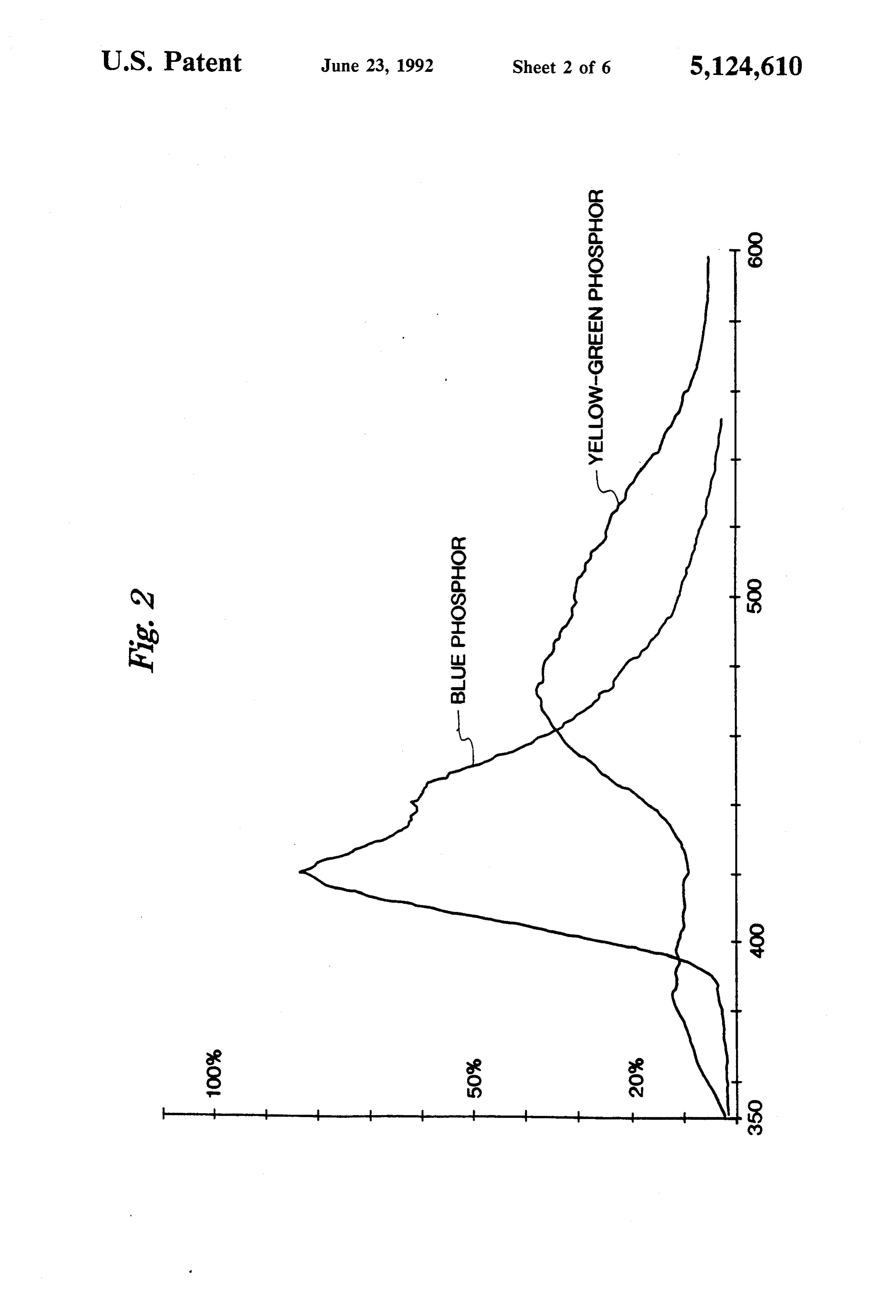
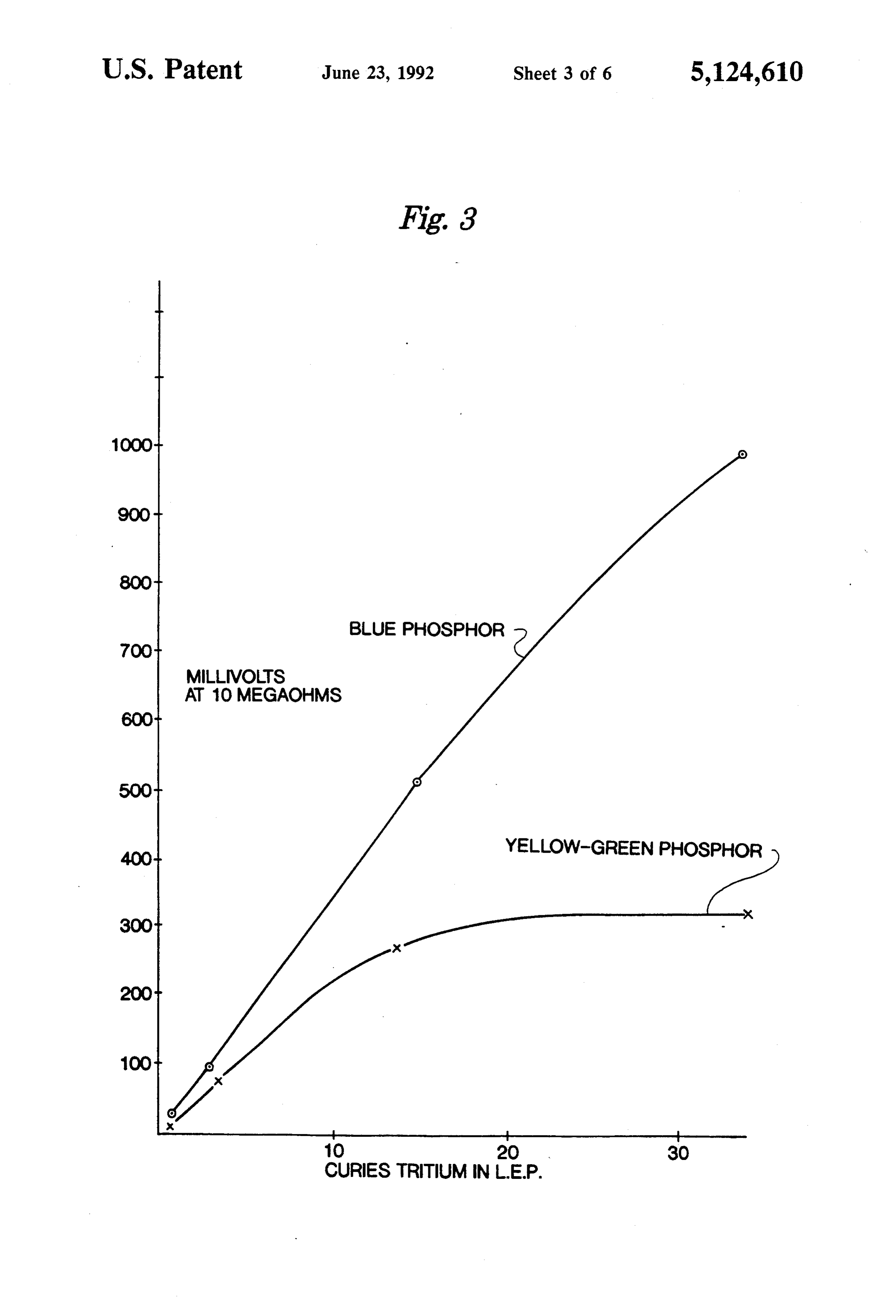
ries. The low emissivity and high energy density of the DESCRIPTION OF THE DRAWINGS preferred embodiment utilizing a tritiated organic poly mer to which an organic phosphor or scintillant is FIG. 1 is a cut-away pictorial view of a light emitting bonded enable the electrical energy source to realisti 50 polymer electrical energy source in accordance with cally utilize 4.0% or more of the theoretical 3.6 amp the preferred embodiment of the present invention. hours of electrical energy that are present in each curie FIG. 2 is a graph showing the spectral emissions of a of tritium. In this embodiment, an electrical energy various phosphors used as scintillators in the light emit source having 100 curies of tritium is capable of provid ting polymer.
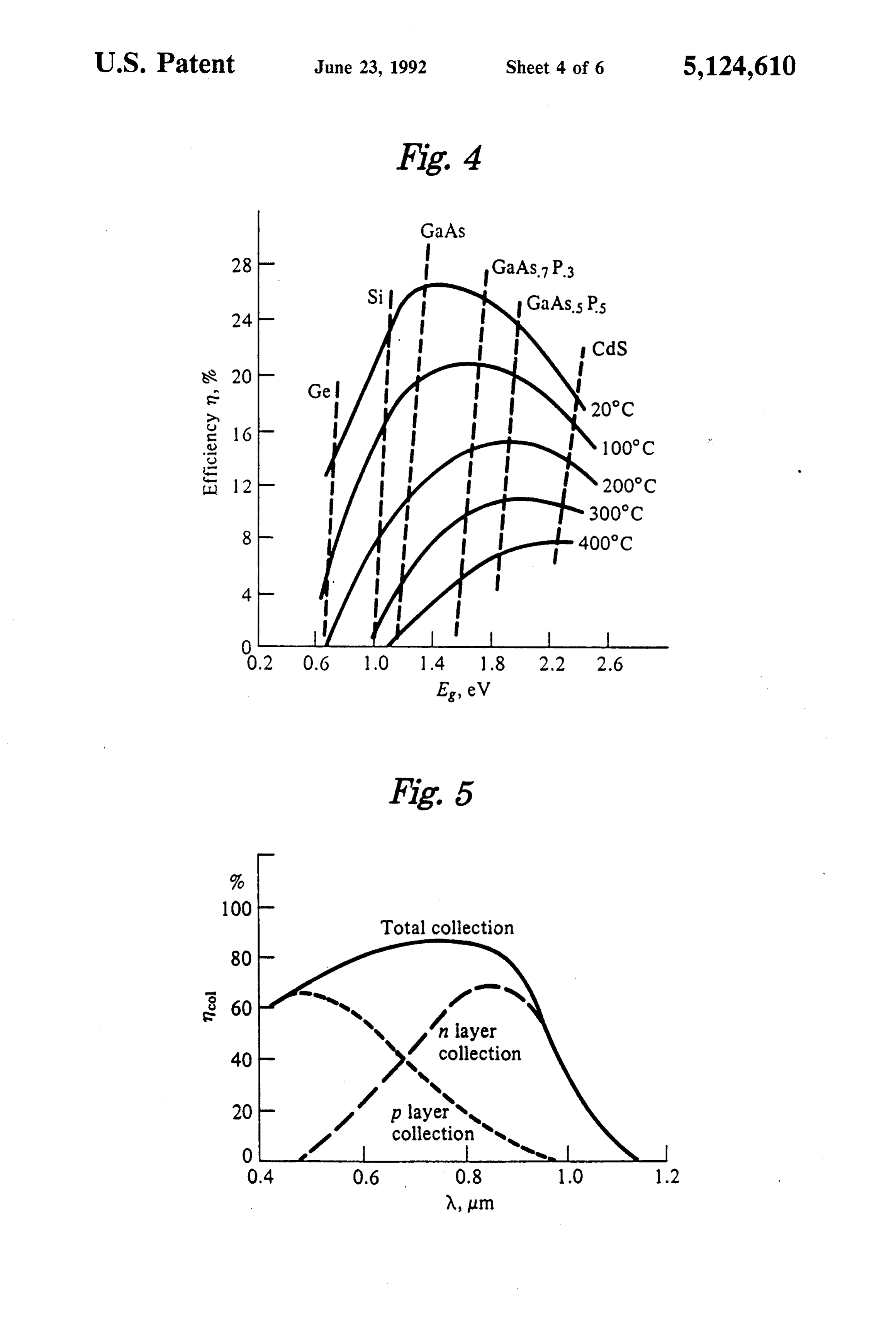
ing 1 microwatt of power at 1 volt and 1 microamp for 55 FIG. 3 is a graph showing the relative scintillation the entire lifetime of the electrical energy source, ap efficiencies for each of the phosphors shown in FIG. 2. proximately 20 years. FIG. 4 is a graph showing the maximum theoretical Because the electrical energy generated by the pres conversion efficiencies for various semiconductor mate ent invention is dependent upon the rate of emission of rials.
photons from the light emitting polymer (which is in 60 FIG. 5 is a graph showing the collection efficiency of turn dependent upon the rate of beta-emissions from the a photovoltaic cell as a function of the wavelength of radioisotope used to activate the light emitting poly the incident light.
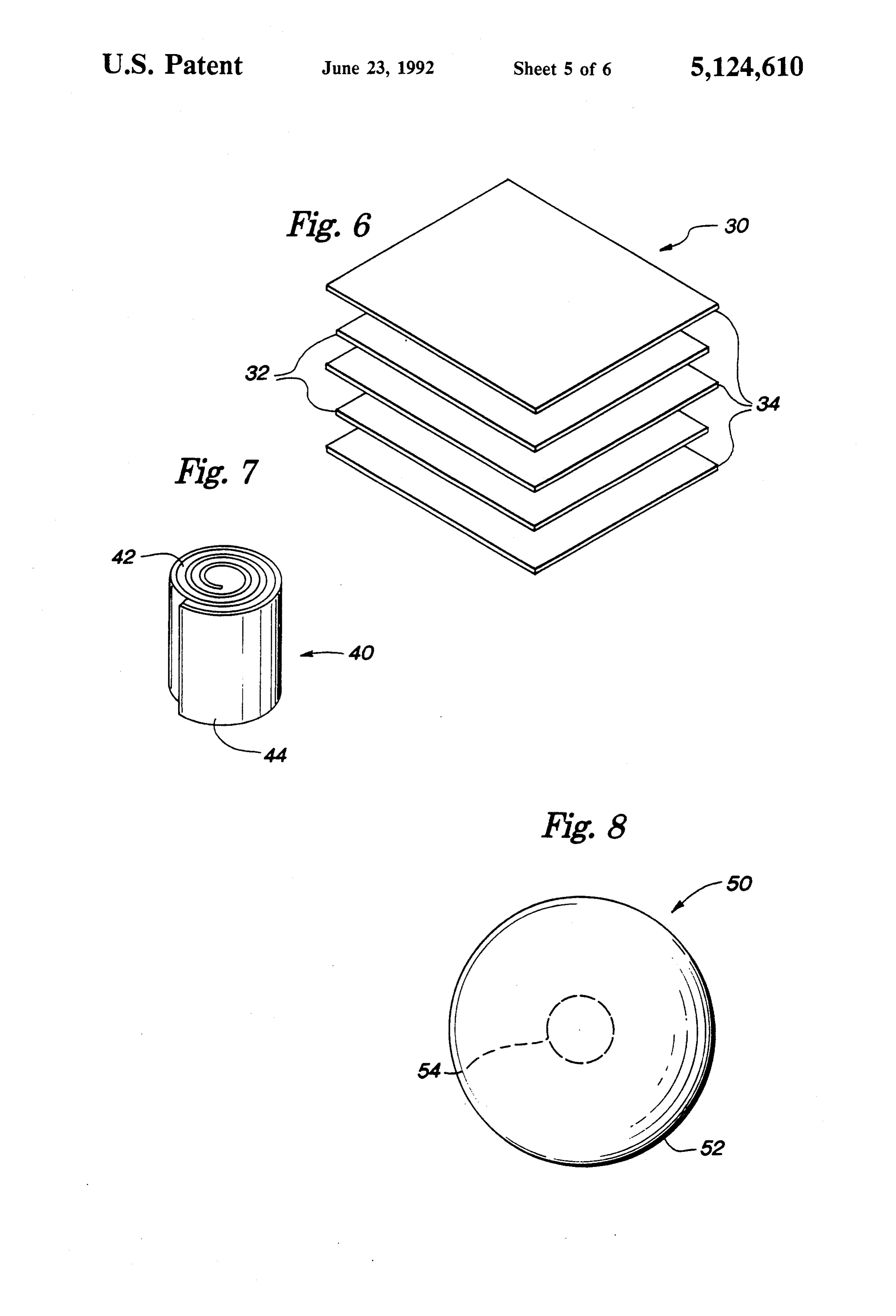
mer), the amount of energy available is constant and FIG. 6 is a pictorial view showing a multiple-layer determinable. In addition to providing a unique source configuration of an alternative embodiment of the pres of electrical energy for CMOS, NMOS and other low 65 ent invention arranged to allow for dual-sided utiliza power types of electronic circuitry, the ouput stability tion of the photovoltaic cells.
of the electrical energy source of the present invention FIG. 7 is a pictorial view of an alternative embodi makes it ideally suited for applications that require a ment of the present invention showning the light emit
Page 11
ting polymer and the photovoltaic cell in spiral jelly hereby incorporated by reference herein. Those aspects roll configuration. of the LEP material 12 that allow it to be used effec FIG. 8 is a pictorial view of an alternative embodi tively in the present invention are discussed below in ment of the present invention showing the light emitting connection with the various design considerations set polymer cast about the photovoltaic cell in a spherical forth above.
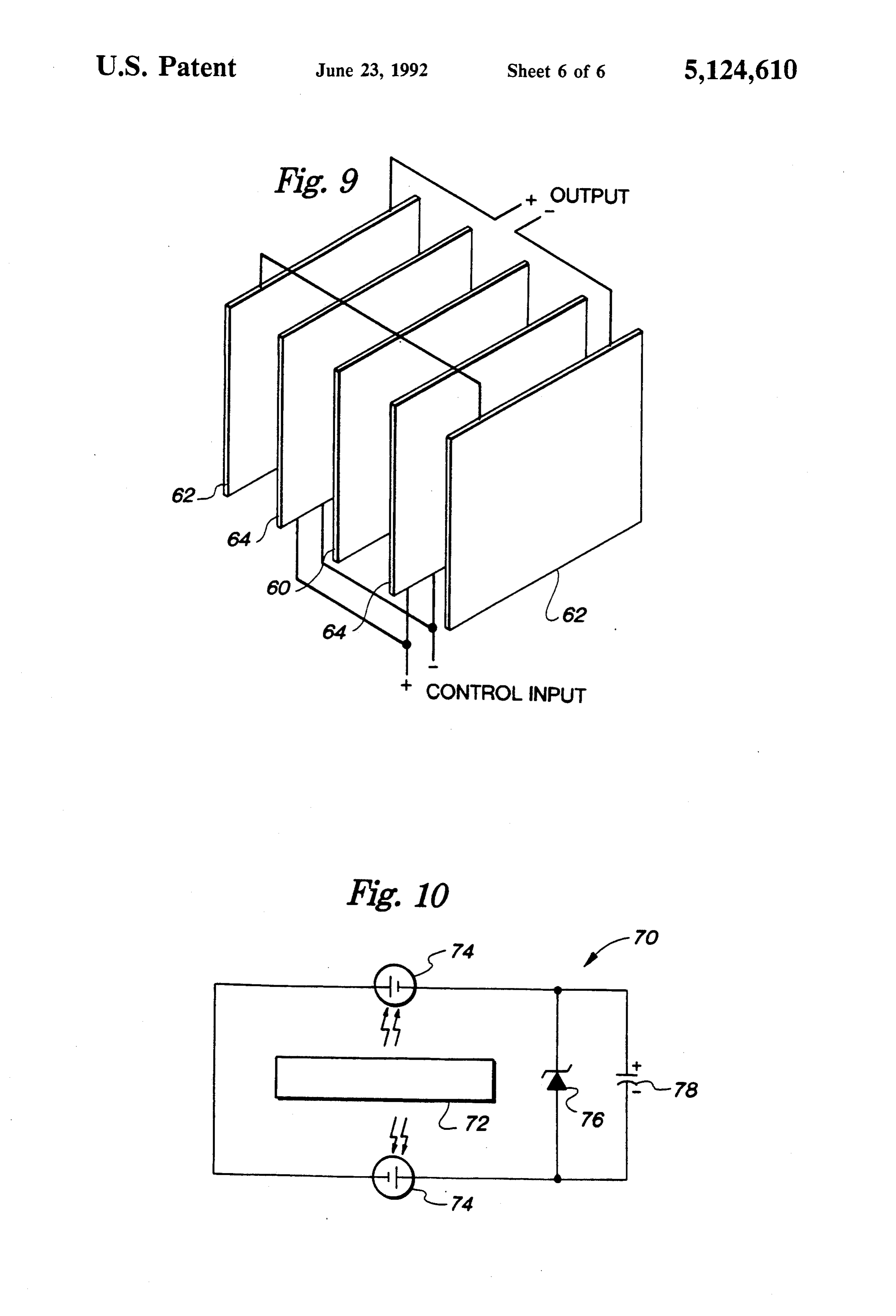
arrangement. In the preferred embodiment, the photovoltaic cells FIG. 9 is a schematic view showing another alterna 14 and 16 are amorphous thin-film silicon solar cells, tive embodiment of the present invention including an Model No. 035-01581-01, available from ARCO Solar, optical control means. Inc., Chatsworth, Calif., or their equivalent. These cells FIG. 10 is a circuit diagram of the electrical energy O have their highest efficiency conversion (greater than source of the present invention showing the addition of 20%) in the blue range of the spectrum of visible light to other circuit elements. match the frequency bandwidth of the emitted light of DESCRIPTTION OF THE PREFERRED LEP material incorporting a phosphor that emits in the EMBODIMENTS blue range. While the particular photovoltaic cells 14 15 and 16 in the preferred embodiment have been selected
The present invention is directed to a safe and practi to match the blue range of the spectrum of visible light, cal, long-life, electrical energy source made by the com it should be apparent that other photovoltaic cells may bination of a light emitting polymer,activated by a radi be selected to match the bandwidth of light emitted at oisotope source, with a photovoltaic cell, to produce other frequencies. In particular, as discussed below, it is electrical energy. As will be appreciated, the potential known that a new solar cell, known as the Sunceran II variations of such a combination are numerous. The (trademark), available from Panasonic's Industrial Bat practical feasibility of an electrical energy source in tery Sales Div., is claimed to more efficient than con accordance with the present invention depends upon a ventional amorphous silicon solar cells, especially in the number of consideration, including: (a) the choice of a red range of the spectrum of visible light. suitable long-lived radioisotope, (b) the efficiency of the 25 To maximize the optical transfer between the LEP scintillation process in the polymer, (c) the efficiency of material 12 and the photovoltaic cells 14 and 16, the the photovoltaic cell, (d) radiation damage to the poly surfaces of the photovoltaic cells 14 and 16 not in mer and the photovoltaic cell, (e) the optical mating of contact with the LEP material 12 are coated with a the polymer and the photovoltaic cell, and (f) the geom reflective material, preferably an aluminum paint or etry of the polymer and the photovoltaic cell. Each of 30 equivalent. The edges of the LEP material 12 not in these considerations will be discussed in describing the contact with the photovoltaic cells 14 and 16 are clad preferred embodiment of the present invention. It will with a similar reflective material. The surfaces of the be observed that the use of a light emitting polymer LEP material 12 and the photovoltaic cells 14 and 16 provides an opportunity to effectively design a safe and that abut one another are coated with a contact gel, practical, long-life electrical energy source in response 35 Rheogel 210 C., available from Synthetic Technology to these considerations. Corp., McLain, Va., or its equivalent, as a means for Referring now to FIG. 1, a cut-away pictorial repre optically coupling the surfaces to increase the amount sentation of the preferred embodiment of the present of light that is transmitted from the LEP material 12 to invention is shown. The electrical energy source 10 is the photovoltaic cells 14 and 16.
comprised of a planar sheet of light emitting polymer 40 ("LEP") material 12 that is interposed between a pair of SELECTION OF THE RADIOSOTOPE photovoltaic cells 14 and 16 having planar dimensions The radioisotope that is used in the LEP material 12 similar to the LEP material 12. The photovoltaic cells must produce sufficient scintillations in the LEP mate 14 and 16 and the LEP material 12 are encased in a rial to insure an adequate production of light for absorp sealed case 18, preferably a laser-welded, stainless steel 45 tion by the photovoltaic cells 14 and 16. For safety case, having a pair of electrical contacts 20 and 22 ex purposes, it is desirable that the selected radioisotope be posed on one end of the case 18. The contacts 20 and 22 chemically bonded to the polymer. By chemically are disposed in a pair of ceramic insulators 24 and 26 bonding the radioisotope to the polymer, any undesir and are connected to the photovoltaic cells 14 and 16 in able build-up of the radioisotope is prevented and the such a manner that one of the contacts will provide a 50 concentration levels of the radioisotope will remain positve voltage potential and the other contact will constant no matter what environmental factors the LEP provide a negative voltage potential. material 12 is subjected to. Unlike radioisotopes in a The LEP material 12 comprises a mixture of a poly liquid or gaseous state, the bonding of the radioisotope mer labelled with a tritium and an organic compound to the polymer in the LEP material 12 of the present which emits light energy when subjected to radiation 55 invention prevents the free release of radiation if the generated by the tritium. The organic compound is at material or container is ever broken. The bonding of the least partly bonded to the polymer and the mixture is radioisotope to the organic polymer is expected to re translucent at the specified frequency bandwidth of the sult in NRC approval for the use of higher allowable light energy. Such an LEP material was obtained from levels of radioactive material for radioisotopes in this Amersham International plc, Amersham Place, little format.
Chalfont, Buckinghamshire, England, and pending The radioisotope should have a half-life comparable NRC regulatory approval, may be available from to the desired useful lifetime of the electrical energy Amersham International plc. Such an LEP material is source 10. Because the power is directly proportional to described in the United Kingdom patent application, the rate of decay of the radioisotope in the LEP mate Ser. No. 90/08,268.6 by C. D. Bell and J. H. C. Howes, 65 rial 12, for a given desired power output the rate of entitled TRITIATED LIGHT EMITTING POLY decay should ideally correspond to the power require MER COMPOSITIONS, filed in the British Patent ments of the electrical energy source 10. If the half-life Office on Apr. 11, 1990, the disclosure of which is is too long with respect to the useful life of the electrical
Page 12
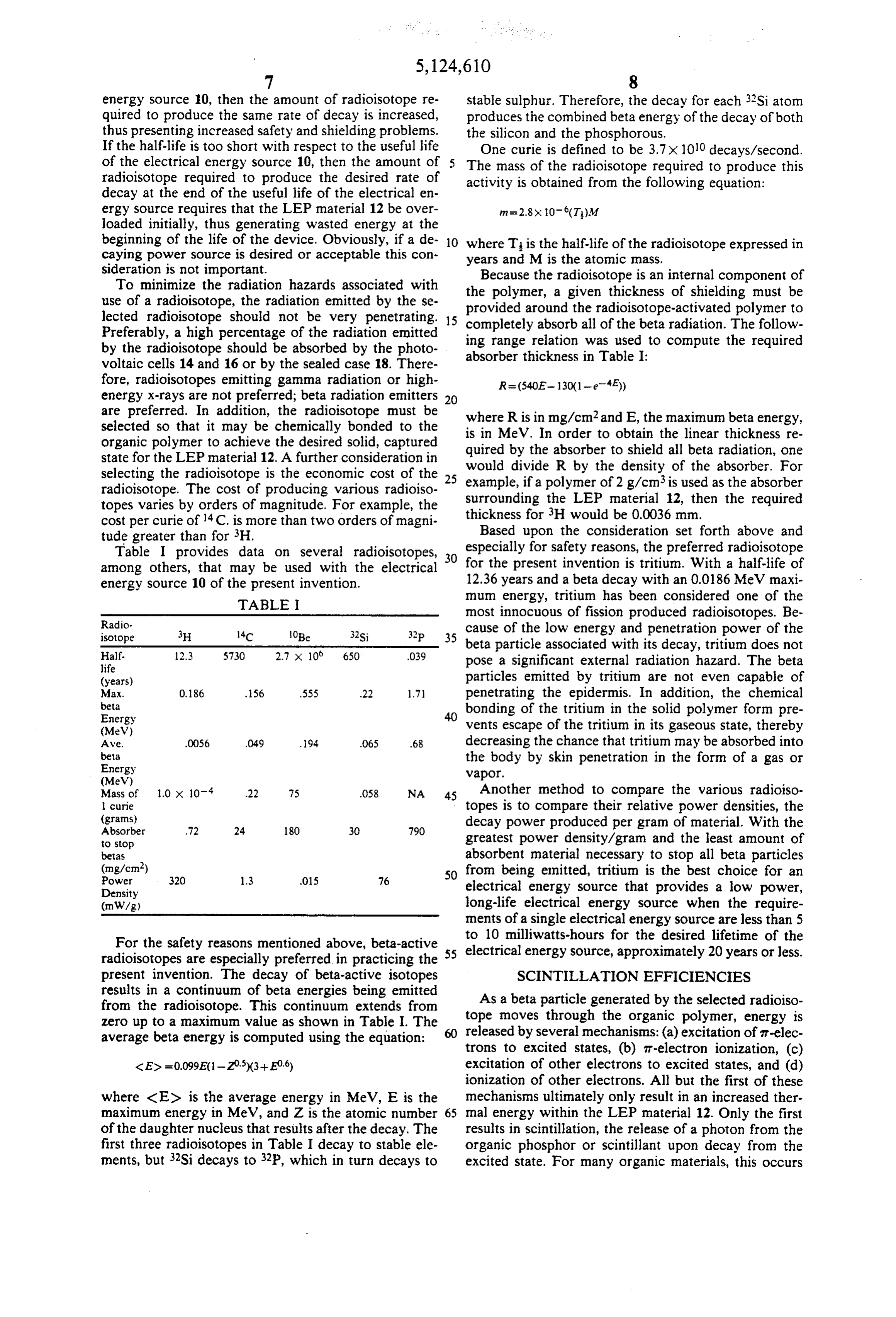
energy source 10, then the amount of radioisotope re stable sulphur. Therefore, the decay for each 32Si atom quired to produce the same rate of decay is increased, produces the combined beta energy of the decay of both thus presenting increased safety and shielding problems. the silicon and the phosphorous. If the half-life is too short with respect to the useful life One curie is defined to be 3.7 x 10¹⁰ decays/second. of the electrical energy source 10, then the amount of 5 The mass of the radioisotope required to produce this radioisotope required to produce the desired rate of activity is obtained from the following equation: decay at the end of the useful life of the electrical en ergy source requires that the LEP material 12 be over loaded initially, thus generating wasted energy at the beginning of the life of the device. Obviously, if a de- 10 where T is the half-life of the radioisotope expressed in caying power source is desired or acceptable this con years and M is the atomic mass.
sideration is not important. Because the radioisotope is an internal component of To minimize the radiation hazards associated with the polymer, a given thickness of shielding must be use of a radioisotope, the radiation emitted by the se provided lected radioisotope should not be very penetrating. 15 completelyaround the radioisotope-activated polymer to Preferably, a high percentage of the radiation emitted ing range relation all absorb was of the beta radiation. The follow used to compute the required by the radioisotope should be absorbed by the photo absorber thickness in Table I: voltaic cells 14 and 16 or by the sealed case 18. There fore, radioisotopes emitting gamma radiation or high energy x-rays are not preferred; beta radiation emitters 20 are preferred. In addition, the radioisotope must be where R is in mg/cm2 and E, the maximum beta energy, selected so that it may be chemically bonded to the is in MeV. In order to obtain the linear thickness re organic polymer to achieve the desired solid, captured quired by the absorber to shield all beta radiation, one state for the LEP material 12. A further consideration in selecting the radioisotope is the economic cost of the 25 would divide R by the density of the absorber. For example, if a polymer of 2 g/cm3 is used as the absorber radioisotope. The cost of producing various radioiso surrounding the LEP material 12, then the required topes varies by orders of magnitude. For example, the thickness for 3H would be 0.0036 mm. cost per curie of C. is more than two orders of magni Based upon the consideration set forth above and tude greater than for H.
Table I provides data on several radioisotopes, especially for the for safety reasons, the preferred radioisotope present invention is tritium. With a half-life of among others, that may be used with the electrical energy source 10 of the present invention. 12.36 years and a beta decay with an 0.0186 MeV maxi TABLE I mum energy, tritium has been considered one of the
Radio most innocuous of fission produced radioisotopes. Be isotope 3H 14C 10Be 32Si 32p 35 cause of the low energy and penetration power of the
beta particle associated with its decay, tritium does not life pose a significant external radiation hazard. The beta (years) particles emitted by tritium are not even capable of Max. 0.86 56 555 .22 1.7 penetrating the epidermis. In addition, the chemical beta
Energy bonding of the tritium in the solid polymer form pre (MeV) vents escape of the tritium in its gaseous state, thereby Ave. 0056 049 .94 065 .68 decreasing the chance that tritium may be absorbed into beta
Energy the body by skin penetration in the form of a gas or vapor.
(MeV)
Mass of 1.0 x 10⁻⁴ .22 75 O58 NA 45 Another method to compare the various radioiso 1 curie (grams) topes is to compare their relative power densities, the
Absorber 72 24 180 30 790 decay power produced per gram of material. With the to stop greatest power density/gram and the least amount of betas
absorbent material necessary to stop all beta particles
Power 320 1.3 O15 76 50 from being emitted, tritium is the best choice for an Density electrical energy source that provides a low power, (nW/g) long-life electrical energy source when the require ments of a single electrical energy source are less than 5 to 10 milliwatts-hours for the desired lifetime of the
For the safety reasons mentioned above, beta-active radioisotopes are especially preferred in practicing the 55 electrical energy source, approximately 20 years or less. present invention. The decay of beta-active isotopes SCINTILLATION EFFICIENCIES results in a continuum of beta energies being emitted As a beta particle generated by the selected radioiso from the radioisotope. This continuum extends from tope moves through the organic polymer, energy is zero up to a maximum value as shown in Table I. The 60 released by several mechanisms: (a) excitation of r-elec average beta energy is computed using the equation:
trons to excited states, (b) T-electron ionization, (c) <ES =0.099E(1-205)(3+E06) excitation of other electrons to excited states, and (d) ionization of other electrons. All but the first of these where <Ed is the average energy in MeV, E is the mechanisms ultimately only result in an increased ther maximum energy in MeV, and Z is the atomic number 65 mal energy within the LEP material 12. Only the first of the daughter nucleus that results after the decay. The results in scintillation, the release of a photon from the first three radioisotopes in Table I decay to stable ele organic phosphor or scintillant upon decay from the ments, but 32Sidecays to 32P, which in turn decays to excited state. For many organic materials, this occurs
Page 13
with a probability of about 10%. Therefore, only about energy in the visible spectrum, it is also possible to use 10-20% of the energy deposited by a beta particle is a scintillant that emits electromagnetic energy in the available for light production. Because it may be neces ultraviolet, infrared, or other frequency bands of the sary to shift the light produced by such scintillations electromagnetic spectrum. Accordingly, the term into the portion of the spectrum to which the photovol "light" as used in this application is intended to encom taic cells 14 and 16 are more sensitive, secondary and pass all frequencies of electromagnetic radiation pro tertiary phosphors may also need to be added to the duced by scintillation activity. For example, if the aver LEP material 12. This may result in further degradation age mean path of a photon emitted in the ultraviolet of the scintillation efficiency of the LEP material 12. spectrum by the primary phosphor is sufficiently great For a more detailed explanation of the operation of 10 to escape the polymer, and if a photovoltaic cell capable scintillators in response to beta radiation, reference is of absorbing energy having a wavelength of 400 nm or made to E. Schrafin, Organic Scintillator Detectors, 1973, less were available, the LEP material 12 might not need pp. 67-74, which is hereby incorporated by reference a secondary phosphor and the energy emitted by the herein. primary phosphor could be used directly to power the In the LEP material 12 of the preferred embodiment, 15 photovoltaic cells 14 and 16. In addition, the bandwidth the scintillation efficiency is increased by bringing the of the emitted light from the LEP material 12 need not primary organic phosphor into a weak bonding with the be limited to monochromatic light. Various combina tritiated organic polymer. Because the beta particle tions of primary and/or secondary phosphors in the emitted by the tritium is of such low energy, the closer LEP material could be used to broaden the bandwidth the tritium is located to the phosphor, the greater the 20 of either or both the intermediary or emitted energy probability that the beta particle will be able to interact from the LEP material 12. Again, the polymer structure with the phosphor. Because the average mean distance of the LEP material allows the LEP material 12 to be of the path of an emitted beta particle is less than 1 designed to achieve these objectives. micron, the probabilities of interaction between the beta PHOTOVOLTAIC CELL EFFICIENCIES particle and the phosphor decrease dramatically unless 25 the phosphor is located within that range. Presently, most of the work, both theoretical and In the preferred embodiment, the LEP material 12 practical, on the design of semiconductor photovoltaic utilizes both a primary and a secondary phosphor. The cells relates to their use as solar cells that are designed primary organic phosphor may be any phosphor or to absorb all of the spectral energy available from the scintillant in the groups PPO, PBD, or POPOP that 30 sun, either at AM0 conditions outside the earth's atmo operates to capture the beta particle and emit a photon sphere, or at AM1 conditions at sea level. It is well in the ultraviolet frequency. The secondary phosphor known that there are both theoretical and practical may either be bonded to or admixed with the organic efficiency limits for such solar cells. In theory, there are polymer and performs a Stokes shift on the emitted only two parameters that will determine the efficiency photon to shift its frequency to the desired frequency of 35 of a solar cell, the band gap energy of the solar cell the light to be emitted by the LEP material 12. The material and the temperature of the cell. For an amor various techniques for performing a Stokes shift are phous silicon solar cell, the bandgap energy of 1.1 eV well known in the art. means that only those photons of wavelengths less than Unlike the prior art techniques of admixing the trit about 1,100 nm are capable of producing electron-hole ium with the phosphor or encapsulating gaseous tritium pairs in the photovoltaic cells that will result in the in a glass vessel, the LEP material 12 utilized by the generation of electrical energy; the remaining energy is present invention maximizes the scintillation efficiency lost, usually in the form of heat. Referring now to FIG. of the beta particle and the organic phosphor by posit 4, the maximum theoretical conversion efficiencies for a ing the tritium relatively near the primary phosphor and variety of photovoltaic cell materials are shown as a by arranging the LEP material 12 such that it is gener 45 function of temperature and energy gap. ally optically transparent at the desired frequency of the In practice, there are a number of other factors that emitted light. In addition, to minimize any optical limit the conversion efficiency of solar cells, including blockage of photons emitted by the LEP material 12, it the excess energy loss for photons that are within the desirable that the catalysts for bonding both the radioi band gap energy, the fill factor loss and the voltage loss sotope and the phosphor or scintillant be completely 50 as a result of the mismatch of the impedance of the load removed or disappear after the polymerization process. and the source. The net result is that typical solar cell Referring now to FIG. 2, the spectral emissions of a efficiencies of only 20% are generally achievable to blue phosphor and a yellow-green phosphor used as the date. Recently, greater efficiencies have been achieved secondary phosphor in the LEP material 12 are shown. for a printed compound thin-film photovoltaic cell uti FIG. 3 shows the relative scintillation efficiencies as a 55 lizing the group II-VI compound semiconductors function of output voltages over various curie levels in CdS/CdTe. These solar cells, known as the Sunceram the LEP material 12 utilizing each of these phosphors. II, are available from Panasonic's Industrial Battery As can be seen, the relative efficiency of the yellow Sales Div., Secaucus, N.J., and utilize an in-layer (CdS) green phosphor decreases with increasing levels of the and a p-layer (CdTe) semiconductor films created by a radioisotope. This effect, known as bleaching, is well 60 film-fabrications process that entails paste application known in the field of scintillation. Obviously, it is desir by screen printing and sintering in a belt-type furnace. able that the phosphor(s) selected for use with the LEP The Sunceram II solar cells have an output five times material 12 should not be subject to bleaching or other higher than conventional amorphous silicon solar cells types of deterioration as a result of activation by the when illuminated by tungsten light. particular radioisotope selected for use in the LEP ma 65 In the present invention, the design parameters of the terial 12. photovoltaic cell do not have to be matched to the It should be noted that although the preferred em entire bandwidth of visible light to optimize absorption bodiments are described in terms of scintillants that emit of the entire solar spectrum. Rather, the design of the
Page 14
photovoltaic cells 14 and 16 may be tailored to the labelied molecules (the lower the better), and (i) radio particular bandwidth and wavelengths of emitted light active concentration level of the polymer. The basic from the LEP material 12. It is well known that differ polymer of the LEP material 12 of the preferred em ent semiconductor materials have different bandgap bodiment is known to have one of the lowest coeffici energies and, hence, will absorb photons of different ents of radiation damage of any polymer. wavelengths (e.g., Si absorbs photons with A < 1.1 in As for the photovoltaic cells, it is well known that and GaAs absorbs photons with 1 <0.9 um). However, radiation energies in excess of 4 KeV can damage the the wavelength of the photon also determines where in p-n junction in the semiconductor material. If the single the p-n junction the photons will be converted into conversion process taught by the prior art were used to electron-hole pairs. For short wavelengths (w = 0.55 10 produce electrical energy, the damage to one cm of a um), most photons will be converted into electron-hole p-n junction caused by the beta particles emitted by a pairs in a narrow region near the surface of the p-layer one curie of tritium would effectively destroy the p-n of the p-n junction. Whereas, at longer wavelengths junction in a relatively short amount of time. In addi (X = 0.9 m), the absorption coefficient for the semicon tion, if a single conversion process were used, the poly ductor is small and absorption takes place mostly in the 15 mer containing the tritium could be no more than n-layer of the p-n junction. FIG. 5 shows the collection micron thick, otherwise the polymer itself would pre efficiency for both the p-layer and the n-layer of a pho vent the beta particles from reaching the p-n junction. tovoltaic cell as a function of the wavelength of the The present invention allows a double conversion pro incident light. The collection efficiency of the photo cess to be used with a low-level light source and still voltaic cell will be influenced by the minority-carrier achieve a conversion efficiency that is equal to or diffusion length of the semiconductor material and by greater than the conversion efficiencies achieved by the absorption coefficient. A large absorption coeffici single conversion processes. By efficiently converting ent leads to heavy absorption near the surface of the p-n the beta particles to photons in the LEP material 12, the junction, resulting in strong collection in the skin layer. present invention simultaneously solves the problems of A small absorption coefficient allows deep penetration 25 radiation damage and the distance that the p-n junction of photons so the base layer of the p-n junction becomes can be located from the energy source. An additional more important in carrier collection. A typical GaAs advantage of utilizing the LEP material 12 of the pres photovoltaic cell produces more of the skin layer effect, ent invention is that the LEP material 12 itself shields and a typical Si photovoltaic cell produces more of the the p-n junction of the semiconductor material of the base layer effect. For a more detailed discussion as to 30 photovoltaic cells 14 and 16 from radiation damage, the effect of wavelength and semiconductor selection thereby increasing the useful life of the electrical energy on the conversion efficiencies of the photovoltaic cell, source 10.
reference is made to Edward S. Yang, Fundamentals of
Semiconductor Devices, pp. 147-162 (1978). OPTICAL MATING CONSIDERATIONS In the present invention, the selection of the primary 35 To maximize the transfer of light emitted by the LEP and secondary phosphors of the LEP material 12 can be material 12, the LEP material 12 must be efficiently made to generate a monochromatic or a narrow band coupled to the photovoltaic cells 14 and 16. This is width of emitted light, the frequency of which can be achieved by the use of a means for optically coupling matched to the particular type of photovoltaic cell 14 the LEP material 12 with the photovoltaic cells 14 and and 16 desired. This matching depends upon the type of 40 16 and by creating smooth surfaces on both the LEP conversion desired (base vs. skin effect), the efficiency material 12 and the photovoltaic cells 14 and 16. of the semiconductor material in the bandwidth, and The primary purpose of the means for optically cou other considerations relating to the design of the electri pling the LEP material 12 and the photovoltaic cells 14 cal energy source 10, including the curie loading, safety and 16 is to insure that as much of the light that is emit factors, the cost, and the environment in which the 45 ted by the LEP material 12 will be allowed to pass device will be operated. Although such a device is not through to the light collecting surface of the photovol currently available, it may be possible to provide a taic cells 14 and 16. Unlike prior art devices, the means double-sided, monochromatic, bandwidth-matched for optically coupling the two materials is not required photovoltaic cell for use with light emitting polymer in to also serve as a means for isolating the two materials. the present invention that could achieve conversion 50 In one embodiment, an anti-reflective coating matched efficiencies of 60-70% or higher. to the frequency of the emitted light and the indices of POLYMER AND PHOTOVOLTAC CELL refraction of the two materials is used as the means for RADIATION DAMAGE optically coupling the two materials. Where the index The long term performance of a polymer scintillator 55 of refraction of the polymer is nand the index of refrac tion of the photovoltaic cell is n, then the index of can be affected by the accumulated radiation dose de refraction of the anti-reflective coating should be the: posited in the polymer. In addition, a variety of other factors can affect the aging of the polymer. The major variable in pure polymer aging are: (a) radiation inten sity and wavelength distribution; (b) ambient tempera The index of refraction of silicon is about 3.5 and the ture; (c) monomer content; (d) level of other impurities; index of refraction for most polymers is around 1.5. and (e) oxygen concentration in the surrounding atmo Thus, the anti-reflective coating should have an index of sphere. To increase the life of the polymer, the last four refraction of about 2.3. The thickness of the anti-reflec factors should all be minimized. For the LEP material tive coating should be wavelength of the frequency of 12, four additional factors affect the stability and aging 65 the emitted light. A similar effect may also be achieved of the polymer: (f) radiation resistance and purity of the by the use of an optical coupling gel, such as Rheogel scintillators used; (g) wavelength of the emitted light 210C or its equivalent. As with the geometrical consid (the higher the better); (h) presence of multiple tritium erations to be discussed below, the effect on efficiency
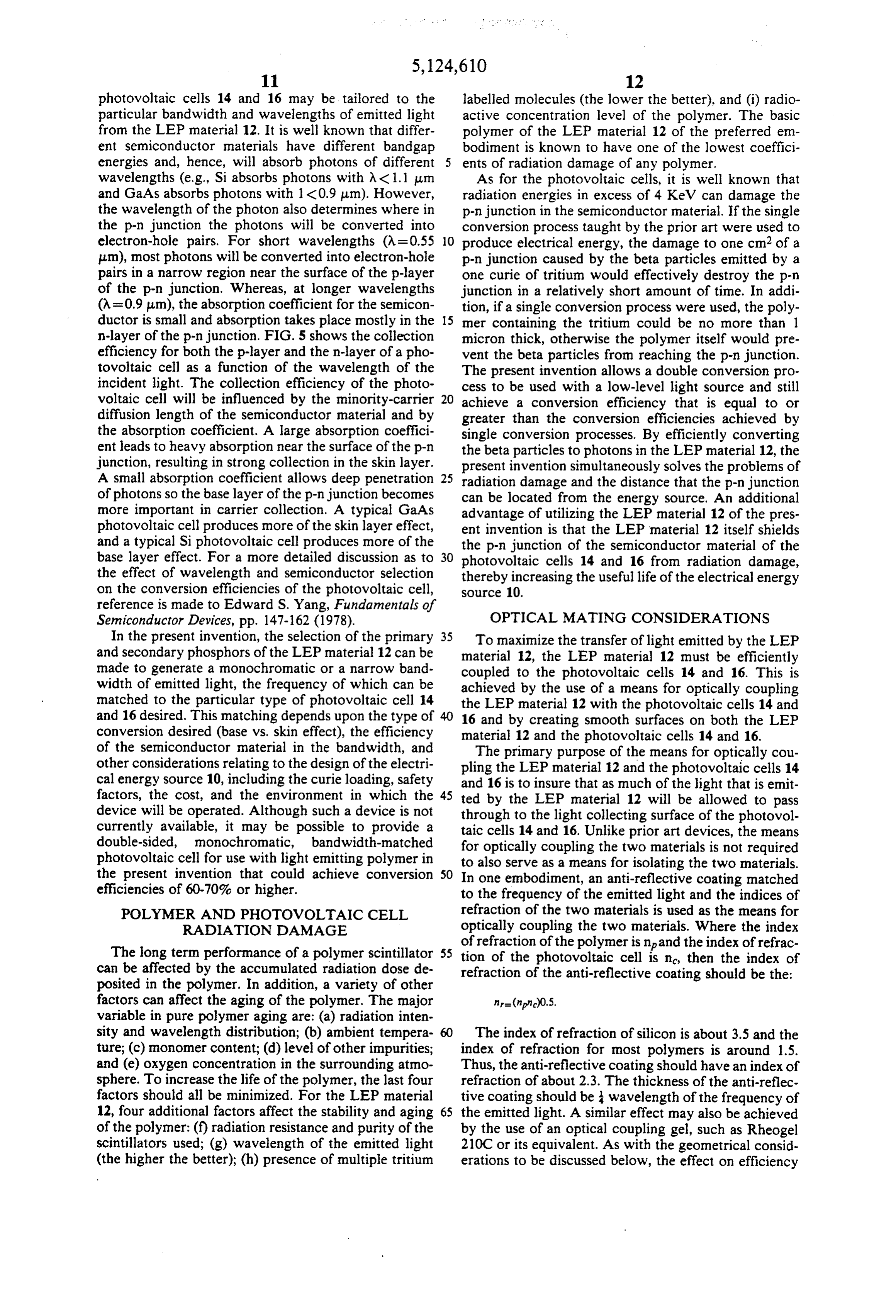
Page 15
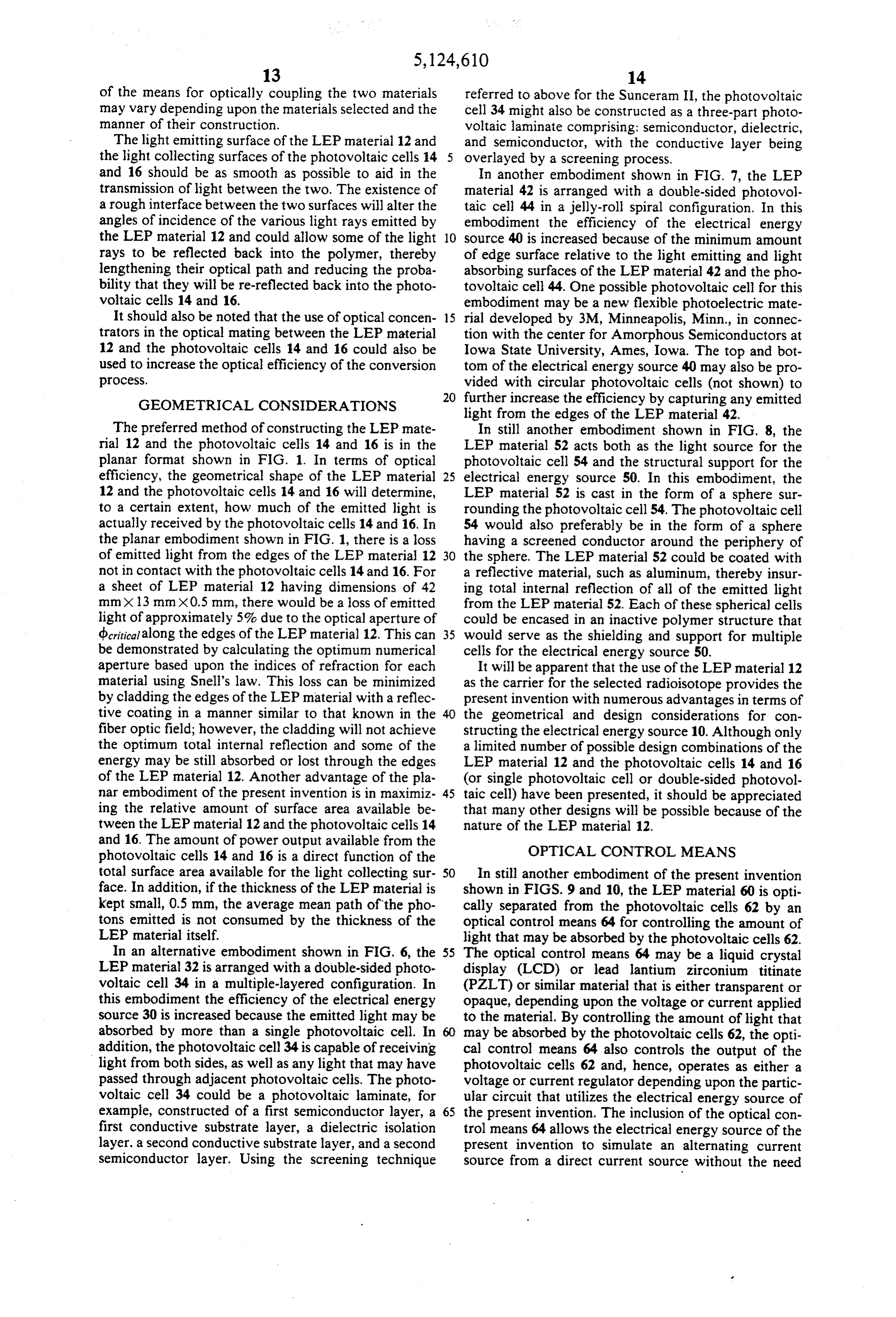
of the means for optically coupling the two materials referred to above for the Sunceram II, the photovoltaic may vary depending upon the materials selected and the cell 34 might also be constructed as a three-part photo manner of their construction. voltaic laminate comprising: semiconductor, dielectric, The light emitting surface of the LEP material 12 and and semiconductor, with the conductive layer being the light collecting surfaces of the photovoltaic cells 14 5 overlayed by a screening process. and 16 should be as smooth as possible to aid in the In another embodiment shown in FIG. 7, the LEP transmission of light between the two. The existence of material 42 is arranged with a double-sided photovol a rough interface between the two surfaces will alter the taic cell 44 in a jelly-roll spiral configuration. In this angles of incidence of the various light rays emitted by embodiment the efficiency of the electrical energy the LEP material 12 and could allow some of the light 10 source 40 is increased because of the minimum amount rays to be reflected back into the polymer, thereby of edge surface relative to the light emitting and light lengthening their optical path and reducing the proba absorbing surfaces of the LEP material 42 and the pho bility that they will be re-reflected back into the photo tovoltaic cell 44. One possible photovoltaic cell for this voltaic cells 14 and 16. embodiment may be a new flexible photoelectric mate It should also be noted that the use of optical concen 15 rial developed by 3M, Minneapolis, Minn., in connec trators in the optical mating between the LEP material tion with the center for Amorphous Semiconductors at 12 and the photovoltaic cells 14 and 16 could also be Iowa State University, Ames, Iowa. The top and bot used to increase the optical efficiency of the conversion tom of the electrical energy source 40 may also be pro process. vided with circular photovoltaic cells (not shown) to 20 further increase the efficiency by capturing any emitted
GEOMETRICAL CONSIDERATIONS
light from the edges of the LEP material 42.
The preferred method of constructing the LEP mate In still another embodiment shown in FIG. 8, the rial 12 and the photovoltaic cells 14 and 16 is in the LEP material 52 acts both as the light source for the planar format shown in FIG. 1. In terms of optical photovoltaic cell 54 and the structural support for the efficiency, the geometrical shape of the LEP material 25 electrical energy source 50. In this embodiment, the 12 and the photovoltaic cells 14 and 16 will determine, LEP material 52 is cast in the form of a sphere sur to a certain extent, how much of the emitted light is rounding the photovoltaic cell 54. The photovoltaic cell actually received by the photovoltaic cells 14 and 16. In 54 would also preferably be in the form of a sphere the planar embodiment shown in FIG. 1, there is a loss having a screened conductor around the periphery of of emitted light from the edges of the LEP material 12 30 the sphere. The LEP material 52 could be coated with not in contact with the photovoltaic cells 14 and 16. For a reflective material, such as aluminum, thereby insur a sheet of LEP material 12 having dimensions of 42 ing total internal reflection of all of the emitted light mm x 13 mm x 0.5 mm, there would be a loss of emitted from the LEP material 52. Each of these spherical cells light of approximately 5% due to the optical aperture of could be encased in an inactive polymer structure that dcritical along the edges of the LEP material 12. This can 35 would serve as the shielding and support for multiple be demonstrated by calculating the optimum numerical cells for the electrical energy source 50. aperture based upon the indices of refraction for each It will be apparent that the use of the LEP material 12 material using Snell's law. This loss can be minimized as the carrier for the selected radioisotope provides the by cladding the edges of the LEP material with a reflec present invention with numerous advantages in terms of tive coating in a manner similar to that known in the the geometrical and design considerations for con fiber optic field; however, the cladding will not achieve structing the electrical energy source 10. Although only the optimum total internal reflection and some of the a limited number of possible design combinations of the energy may be still absorbed or lost through the edges LEP material 12 and the photovoltaic cells 14 and 16 of the LEP material 12. Another advantage of the pla (or single photovoltaic cell or double-sided photovol nar embodiment of the present invention is in maximiz 45 taic cell) have been presented, it should be appreciated ing the relative amount of surface area available be that many other designs will be possible because of the tween the LEP material 12 and the photovoltaic cells 14 nature of the LEP material 12.
and 16. The amount of power output available from the OPTICAL CONTROL MEANS photovoltaic cells 14 and 16 is a direct function of the total surface area available for the light collecting sur 50 In still another embodiment of the present invention face. In addition, if the thickness of the LEP material is shown in FIGS. 9 and 10, the LEP material 60 is opti kept small, 0.5 mm, the average mean path of the pho cally separated from the photovoltaic cells 62 by an tons emitted is not consumed by the thickness of the optical control means 64 for controlling the amount of LEP material itself. light that may be absorbed by the photovoltaic cells 62. In an alternative embodiment shown in FIG. 6, the 55 The optical control means 64 may be a liquid crystal LEP material 32 is arranged with a double-sided photo display (LCD) or lead lantium zirconium titinate voltaic cell 34 in a multiple-layered configuration. In (PZLT) or similar material that is either transparent or this embodiment the efficiency of the electrical energy opaque, depending upon the voltage or current applied source 30 is increased because the emitted light may be to the material. By controlling the amount of light that absorbed by more than a single photovoltaic cell. In may be absorbed by the photovoltaic cells 62, the opti addition, the photovoltaic cell 34 is capable of receiving cal control means 64 also controls the output of the light from both sides, as well as any light that may have photovoltaic cells 62 and, hence, operates as either a passed through adjacent photovoltaic cells. The photo voltage or current regulator depending upon the partic voltaic cell 34 could be a photovoltaic laminate, for ular circuit that utilizes the electrical energy source of example, constructed of a first semiconductor layer, a 65 the present invention. The inclusion of the optical con first conductive substrate layer, a dielectric isolation trol means 64 allows the electrical energy source of the layer, a second conductive substrate layer, and a second present invention to simulate an alternating current semiconductor layer. Using the screening technique source from a direct current source without the need
Page 16
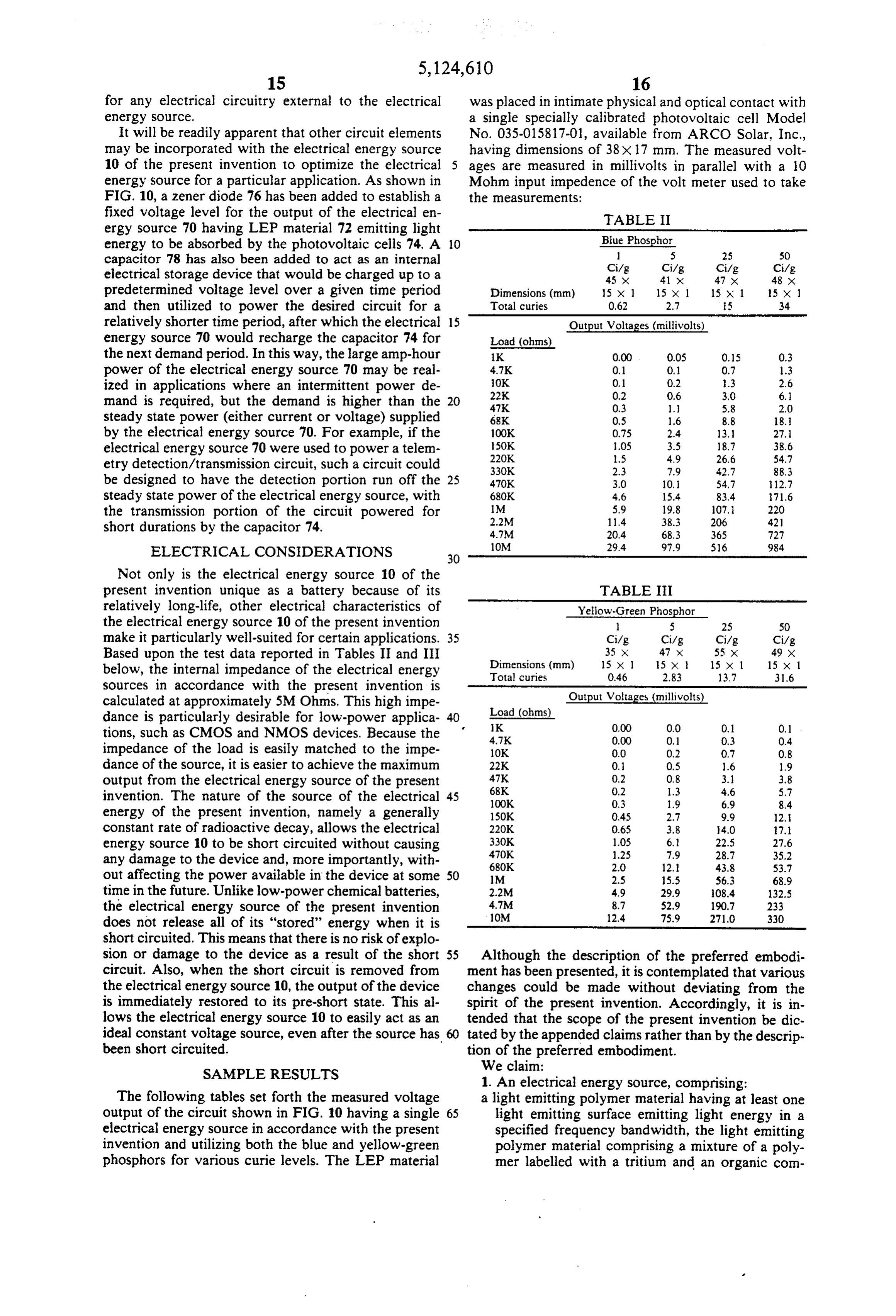
for any electrical circuitry external to the electrical was placed in intimate physical and optical contact with energy source. a single specially calibrated photovoltaic cell Model It will be readily apparent that other circuit elements No. 035-015817-01, available from ARCO Solar, Inc., may be incorporated with the electrical energy source having dimensions of 38x17 mm. The measured volt 10 of the present invention to optimize the electrical ages are measured in millivolts in parallel with a 10 energy source for a particular application. As shown in Mohm input impedence of the volt meter used to take FIG. 10, a zener diode 76 has been added to establish a the measurements:
fixed voltage level for the output of the electrical en TABLE II ergy source 70 having LEP material 72 emitting light energy to be absorbed by the photovoltaic cells 74. A 10 Blue Phosphor
capacitor 78 has also been added to act as an internal Ci/g Ci/g Ci/g Ci/g electrical storage device that would be charged up to a 4.5 x 41 x 47 X 48 X predetermined voltage level over a given time period Dimensions (mm) 15 x 1 15 x 1 15 x 1 SX 1 and then utilized to power the desired circuit for a Total curies 0.62 2.7 5 34 relatively shorter time period, after which the electrical 15 Output Voltages (millivolts) energy source 70 would recharge the capacitor 74 for Load (ohms) the next demand period. In this way, the large amp-hour K 0.00 0.05 0.15 0.3 power of the electrical energy source 70 may be real 4.7K 0.1 0. 0.7 1.3 ized in applications where an intermittent power de 10K
mand is required, but the demand is higher than the 20 47K 0.3 l. 5.8 2.0 steady state power (either current or voltage) supplied 68K 0.5 1.6 8.8 18. by the electrical energy source 70. For example, if the 100K 0.75 2.4 13. 27. electrical energy source 70 were used to power a telem 150K
etry detection/transmission circuit, such a circuit could 330K 2.3 7.9 42.7 88.3 be designed to have the detection portion run off the 25 470K 3.0 10, 54.7 12.7 steady state power of the electrical energy source, with 680K 4.6 15.4 83.4 71.6 the transmission portion of the circuit powered for M
short durations by the capacitor 74. 4.7M 20.4 68.3 365 727 ELECTRICAL CONSIDERATIONS 10M 29.4 97.9 56 984
Not only is the electrical energy source 10 of the present invention unique as a battery because of its TABLE III relatively long-life, other electrical characteristics of Yellow-Green Phosphor the electrical energy source 10 of the present invention 5 25 50 make it particularly well-suited for certain applications. 35 Ci/g Ci/g Ci/g Ci/g Based upon the test data reported in Tables II and III Dimensions (mm)
below, the internal impedance of the electrical energy Total curies 0.46 2.83 13.7 31.6 sources in accordance with the present invention is Output Voltages (millivolts) calculated at approximately 5M Ohms. This high impe dance is particularly desirable for low-power applica Load (ohms)
tions, such as CMOS and NMOS devices. Because the 4.7K 0.00 0.1 0.3 0.4 impedance of the load is easily matched to the impe 10K 0.0 0.2 O. 0.8 dance of the source, it is easier to achieve the maximum 22K 0. 0.5 1.6 1.9 output from the electrical energy source of the present 47K
invention. The nature of the source of the electrical 45 100K 0.3 1.9 6.9 8.4 energy of the present invention, namely a generally 1SOK 0.45 2.7 9.9 12, constant rate of radioactive decay, allows the electrical 220K 0.65 3.8 4.0 7. energy source 10 to be short circuited without causing 330K
any damage to the device and, more importantly, with 680K 2.0 12. 43.8 53.7 out affecting the power available in the device at some 50 1M 2.5 5.5 56.3 68.9 time in the future. Unlike low-power chemical batteries, 2.2M 4.9 29.9 08.4 132.5 the electrical energy source of the present invention 4.7M
does not release all of its "stored" energy when it is short circuited. This means that there is no risk of explo sion or damage to the device as a result of the short 55 Although the description of the preferred embodi circuit. Also, when the short circuit is removed from ment has been presented, it is contemplated that various the electrical energy source 10, the output of the device changes could be made without deviating from the is immediately restored to its pre-short state. This al spirit of the present invention. Accordingly, it is in lows the electrical energy source 10 to easily act as an tended that the scope of the present invention be dic ideal constant voltage source, even after the source has tated by the appended claims rather than by the descrip been short circuited. tion of the preferred embodiment.
We claim:
SAMPLE RESULTS
1. An electrical energy source, comprising:
The following tables set forth the measured voltage a light emitting polymer material having at least one output of the circuit shown in FIG. 10 having a single 65 light emitting surface emitting light energy in a electrical energy source in accordance with the present specified frequency bandwidth, the light emitting invention and utilizing both the blue and yellow-green polymer material comprising a mixture of a poly phosphors for various curie levels. The LEP material mer labelled with a tritium and an organic con
Page 17
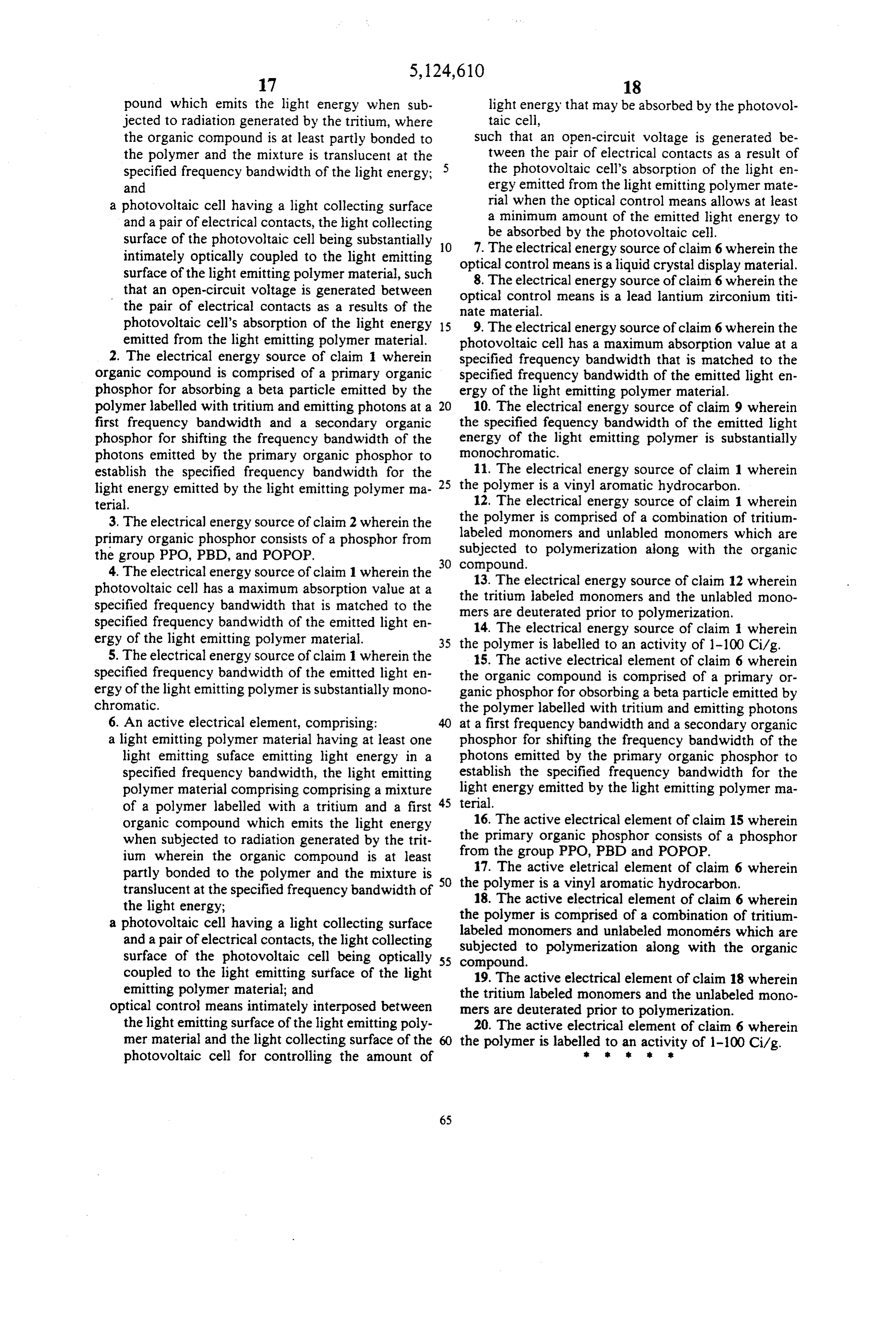
pound which emits the light energy when sub light energy that may be absorbed by the photovol jected to radiation generated by the tritium, where taic cell, the organic compound is at least partly bonded to such that an open-circuit voltage is generated be the polymer and the mixture is translucent at the tween the pair of electrical contacts as a result of specified frequency bandwidth of the light energy; the photovoltaic cell's absorption of the light en and ergy emitted from the light emitting polymer mate a photovoltaic cell having a light collecting surface rial when the optical control means allows at least and a pair of electrical contacts, the light collecting a minimum amount of the emitted light energy to surface of the photovoltaic cell being substantially 10 be absorbed by the photovoltaic cell. 7. The electrical energy source of claim 6 wherein the intimately optically coupled to the light emitting optical surface of the light emitting polymer material, such control means is a liquid crystal display material. 8. The electrical energy source of claim 6 wherein the that an open-circuit voltage is generated between optical control means is a lead lantium zirconium titi the pair of electrical contacts as a results of the nate material.
photovoltaic cell's absorption of the light energy 15 9. The electrical energy source of claim 6 wherein the emitted from the light emitting polymer material. photovoltaic cell has a maximum absorption value at a 2. The electrical energy source of claim 1 wherein specified frequency bandwidth that is matched to the organic compound is comprised of a primary organic specified frequency bandwidth of the emitted light en phosphor for absorbing a beta particle emitted by the ergy of the light emitting polymer material. polymer labelled with tritium and emitting photons at a 10. The electrical energy source of claim 9 wherein first frequency bandwidth and a secondary organic the specified fequency bandwidth of the emitted light phosphor for shifting the frequency bandwidth of the energy of the light emitting polymer is substantially photons emitted by the primary organic phosphor to monochromatic.
establish the specified frequency bandwidth for the 25 11. The electrical energy source of claim 1 wherein light energy emitted by the light emitting polymer ma the polymer is a vinyl aromatic hydrocarbon. terial. 12. The electrical energy source of claim 1 wherein 3. The electrical energy source of claim 2 wherein the the polymer is comprised of a combination of tritium primary organic phosphor consists of a phosphor from labeled monomers and unlabled monomers which are subjected to polymerization along with the organic the group PPO, PBD, and POPOP.
4. The electrical energy source of claim 1 wherein the compound.
photovoltaic cell has a maximum absorption value at a the13.tritium
The electrical energy source of claim 12 wherein labeled monomers and the unlabled mono specified frequency bandwidth that is matched to the mers are deuterated prior to polymerization. specified frequency bandwidth of the emitted light en 14. The electrical energy source of claim 1 wherein ergy of the light emitting polymer material. 35 the polymer is labelled to an activity of 1-100 Ci/g. 5. The electrical energy source of claim 1 wherein the 15. The active electrical element of claim 6 wherein specified frequency bandwidth of the emitted light en the organic compound is comprised of a primary or ergy of the light emitting polymer is substantially mono ganic phosphor for obsorbing a beta particle emitted by chromatic. the polymer labelled with tritium and emitting photons 6. An active electrical element, comprising: at a first frequency bandwidth and a secondary organic a light emitting polymer material having at least one phosphor for shifting the frequency bandwidth of the light emitting suface emitting light energy in a photons emitted by the primary organic phosphor to specified frequency bandwidth, the light emitting establish the specified frequency bandwidth for the polymer material comprising comprising a mixture light energy emitted by the light emitting polymer ma of a polymer labelled with a tritium and a first 45 terial.
organic compound which emits the light energy 16. The active electrical element of claim 15 wherein when subjected to radiation generated by the trit the primary organic phosphor consists of a phosphor ium wherein the organic compound is at least from the group PPO, PBD and POPOP.
partly bonded to the polymer and the mixture is 50 the17.polymer
The active eletrical element of claim 6 wherein is a vinyl aromatic hydrocarbon.
translucent at the specified frequency bandwidth of 18. The active electrical element of claim 6 wherein the light energy;
a photovoltaic cell having a light collecting surface the polymer is comprised of a combination of tritium labeled monomers and unlabeled monomers which are and a pair of electrical contacts, the light collecting surface of the photovoltaic cell being optically 55 subjected compound.
to polymerization along with the organic coupled to the light emitting surface of the light 19. The active electrical element of claim 18 wherein emitting polymer material; and the tritium labeled monomers and the unlabeled mono optical control means intimately interposed between mers are deuterated prior to polymerization. the light emitting surface of the light emitting poly 20. The active electrical element of claim 6 wherein mer material and the light collecting surface of the 60 the polymer is labelled to an activity of 1-100 Ci/g. photovoltaic cell for controlling the amount of it
Provenance
- Collection
- Cited prior art
- Original PDF
- patentimages.storage.googleapis.com →
- Filed
- 1991-03-04
- Pages
- 17
- Method
- pdftotext (the PDF's own text layer) + pdftoppm 300dpi page scans
- Source
- Google Patents bibliographic record
- Granted
- 1992-06-23
- Inventors
- Jerry J. Conley; Gary B. Mortensen; EF Johnson Co
- Transcribed from
- patentimages.storage.googleapis.com →