patent · US5091018
Tandem photovoltaic solar cell with III-V diffused junction booster cell
25 February 1992
Page 1 — bibliographic record
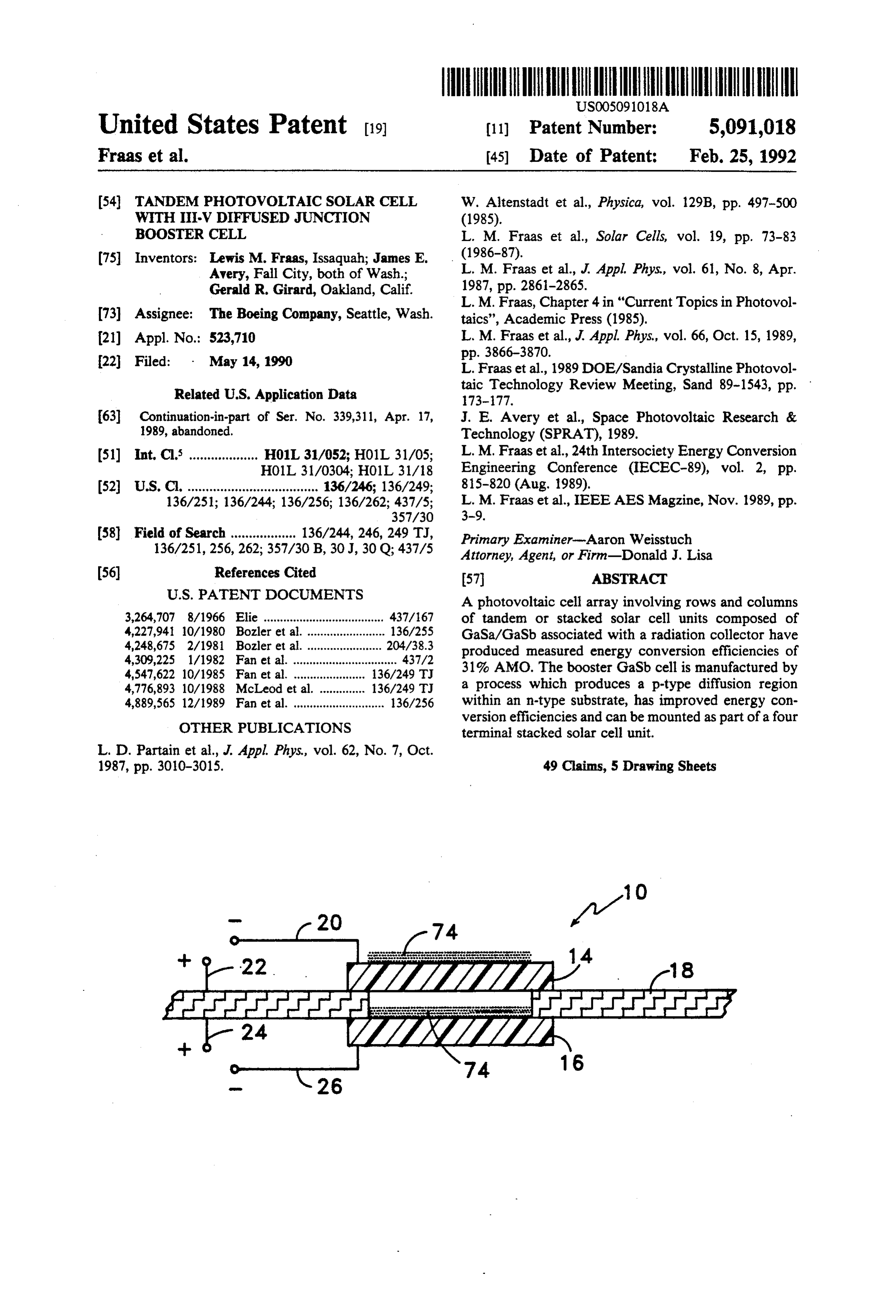
United States Patent (19) 11 Patent Number: 5,091,018 Fraas et al. (45) Date of Patent: Feb. 25, 1992 54 TANDEM PHOTOVOLTAIC SOLAR CELL W. Altenstadt et al., Physica, vol. 129B, pp. 497-500 WITH III-V DIFFUSED JUNCTION (1985).
BOOSTER CELL L. M. Fraas et al., Solar Cells, vol. 19, pp. 73-83 (75 Inventors: Lewis M. Fraas, Issaquah; James E. . (1986-87).
Avery, Fall City, both of Wash.; L. M. Fraas et al., J. Appl. Phys, vol. 61, No. 8, Apr. Gerald R. Girard, Oakland, Calif. 1987, pp. 2861-2865.
L. M. Fraas, Chapter 4 in "Current Topics in Photovol 73 Assignee: The Boeing Company, Seattle, Wash. taics', Academic Press (1985). 21) Appl. No.: 523,710 L. M. Fraas et al., J. Appl. Phys, vol. 66, Oct. 15, 1989, ar. . pp. 3866-3870.
22 Filed: - May 14, 1990 L. Fraas et al., 1989 DOE/Sandia Crystalline Photovol Related U.S. Application Data Ethnology Review Meeting, Sand 89-1543, pp. 63 Continuation-in-part of Ser. No. 339,311, Apr. 17, J. E. Avery et al., Space Photovoltaic Research & 1989, abandoned. Technology (SPRAT), 1989.
51) Int, Cl. ................... H01L 31/052, H01L 31/05; L. M. Fraas et al., 24th Intersociety Energy Conversion H01L 31/0304; HOlL 31/18 Engineering Conference (IECEC-89), vol. 2, pp.
52 U.S.C. .................................... 136/246; 136/249; 815-820 (Aug. 1989).
136/251; 136/244; 136/256; 136/262; 437/5; M. Fraas et al., IEEE AES Magzine, Nov. 1989, pp.
136/251,256, 262,357/30 B, 30J, 30 Q;437/5 C initiatory, (56) References Cited 57 ABSTRACT
3,264,707 8/1966 Elie ............ 437/167 of tandem or stacked solar cell units composed of 4,227,941 10/1980 Bozler et al. .. - - - - 136/2:55 GaSa/GaSb associated with a radiation collector have 4,248,675 2/1981 Bozler et al. ... "' produced measured energy conversion efficiencies of
....... ... 136/249 TJ4; 31%o AMO.. Th ter GaSb
The booster GaSb cell cell isi manufactured factured bby 4,776,893 10/1988 McLeod et al. ... 136/249 r a process which produces a p-type diffusion region 4,889,565 12/1989 Fan et al. ............................ 136/256 within an n-type substrate, has improved energy con version efficiencies and can be mounted as part of a four
OTHER PUBLICATIONS terminal stacked solar cell unit.
L. D. Partain et al., J. Appl. Phys, vol. 62, No. 7, Oct.
1987, pp. 3010-3015. 49 Claims, 5 Drawing Sheets
ZZZZZZZZZZZZ w
ZZZZXZZZZZZZ
Page 2
Drawing sheet — no readable text.
Page 3
Drawing sheet — no readable text.
Page 4
Drawing sheet — no readable text.
Page 5
Drawing sheet — no readable text.
Page 6
Drawing sheet — no readable text.
Page 7
The improved results come from a number of refine
TANDEM, PHOTOVOLTAC SOLAR CELL WITH ments constituting light conditioning means which in I-V DFFUSED UNCTION BOOSTER CELL clude modifying the upper or front GaAs cell of the tandem unit to be transparent to energy having a longer
This application is a continuation-in-part of applica wavelength than the wavelength to which GaAs is tion Ser. No. 07/339,311 filed Apr. 17, 1989, now aban responsive, use of multiple layers of anti-reflective coat doned. ings, placing a novel infrared sensitive GaSb booster This invention relates to mechanically stacked, tan cell that has a band gap of about 0.72 eV behind the dem photovoltaic solar cells which converts incident GaAs cell, and attaching a prism or prismatic cover sunlight to electric power preferably with high energy O glass that is aligned with cell grid lines of each cell or at conversion efficiencies, and more particularly to a least the GaAs cell, to deflect incident light rays into novel III-V diffused booster cell, its method of fabrica active cell area.
tion and the tandem interconnection with an improved The invention also provides a method for improving transparent upper photovoltaic cell. the energy conversion efficiency of a GaAs/GaSb tan 15 dem solar cell by using a diffused junction GaSb cell
BACKGROUND which does not have an upper, passivating, epitaxial Several different types and methods of producing overcoat in a tandem concentrator configuration. solar cells are known in the industry. An ongoing objec Still other features of the present invention are to tive of solar cell manufacturers is to improve the con provide a novel cell production method that is scaleable version efficiencies of the solar cells in a cost effective 20 for efficient large volume production for GaSb cells, ae. certain aspects of which are applicable to other III-V More recently, higher energy conversion efficiencies solar cells, and to provide cells produced by that have been obtained with mechanically stacked multi method.
junction solar cells. This mechanical stacking generally Yet another feature of the invention is to provide a consists of stacking a top cell that absorbs higher fre 25 photovoltaic GaSb cell which does not require a passiv quency light (i.e. a high bandgap cell) on a booster cell ation layer, but instead uses a p-dopant such as zinc, the which will absorb the lower frequency light that passes thickness of the layer being reduced in active areas through the top cell (i.e. a low bandgap cell). See Fraas, between grid lines to nearly double the short circuit "Current Topics in Phtovoltaics”, p. 169, Academic current.
Press (1985) Partain et al., “26.1% Solar Cell Efficiency 30 It is another major object of the invention to provide For Ge Mechanically Stacked Under GaAs', 62 J. a novel solar cell array composed of a solar collecting Appl. Phys., p. 3010 (1987). One example of a lower band lens and multiple wafer type cells that are mechanically gap booster cell is germanium (Ge). See Partain, supra, stacked with the upper cell being transparent to pass Another example of a lower band gap booster is gallium infrared energy to the lower cell. The mounting of the antimonide (GaSb). See Fraas et al, "GaSbFilm Grown 35 tandem cells and the current collecting and voltage by Vacuum Chemical Epitaxy Using Triethyl Anti matching arrangements provide a two-terminal device mony And Triethyl Gallium Source', 61 J. Appl. Phys, which may be used also in terrestrial applications where p. 2861 (1987). Theoretical projections of the perfor a world record conversion efficiency of about 34-37% mance of a GaAs on GaSb mechanical stack have been has been measured AM 1.5D (100suns). reported; see Fraas et al, "Near-Term Higher Efficien The preferred embodiment of the present invention cies With Mechanically Stacked Two-Color Solar Bat utilizes a III-V compound semiconductor material, teries', 19 Solar Cells p. 73 (1986-87), but no high per such as gallium antimonide (GaSb), as a substrate for formance booster cells have previously been fabricated. the booster cell. Into a windowed portion of the n-type Copper Indium Diselenide is another booster cell for substrate surface a p-type doping material, such as zinc, GaAs. See U.S. Pat. Nos. 4,680,422 and 4,795,501. 45 is diffused. A passivating layer for GaSb, previously In McLeod et al U.S. Pat. No. 4,776,893 it was pre through to be essential, is not used. A grid in the form sumed that a passivation window of aluminum gallium of parallel lines of conductive material that are in direct antimonide (AlGaSb) would be required for the bottom contact with the p-type material in the diffused region cell. Forming such a passivation window would neces of the semiconductor is connected to the front side sitate the use of a costly, low throughput epitaxial pro SO metallization bus which is on an insulative mask of a cessing to produce the GaSb cells. suitable material such as silicon nitride. A metal contact GaSb photodiodes fabricated by zinc diffusion from a is also formed on the back side of the substrate. Prior to zinc-silica spin on film is described by W. Schmidt auf. coating with an anti-reflective material, the diffused Altenstadt and C. Heinz in Physica 129B, p. 497, 1985. area is etched back to reduce the emitter depth so that . The zinc concentration obtained by that process were 55 the short circuit current will be increased. too low for solar cells. According to a preferred method of fabricating the SUMMARY OF THE INVENTION GaSb cell, the n-type semiconductor material receives a patterned layer of insulative material containing an
Accordingly, the present invention preferably pro opening through which a p-type dopant is diffused. A vides a novel solar cell that overcomes the above defi grid of conductive material is thereafter formed on the ciencies. When located at the focus of a sunlight con diffused area and a bus is placed on the layer of insula centrating lens, the best of the prior art GaAs satellite tive material to contact said grid, but not the semicon solar cells, where air mass effects are 0, i.e. AMO, con ductor material. A metallized surface is formed on the vert about 22% (AMO) of the incident sunlight to elec opposite side of the semiconductor material. Non-met tric power. By the invention disclosed herein, this con 65 allized areas of the diffused portions are etched to in version efficiency has been increased to about 31% crease the short circuit current and anti-reflective layers (AMO, 100 suns D) which is a new world record con are applied to said etched areas to further increase the version efficiency for a satellite photovoltaic device. short circuit current.
Page 8
These and other features of the invention will become As illustrated in FIG. 2, the upper cell may have two more fully apparent from the claims and from the de terminals 20, 22 and the lower cell may have two termi scription as it proceeds in connection with the appended nals 24, 26. The terminal 22 may be connected with drawings. printed circuit wiring on the front side of card 18 while BRIEF DESCRIPTION OF DRAWINGS the terminal 24 is connected with an electrically sepa rate printed circuit wiring on the back side of card 18.
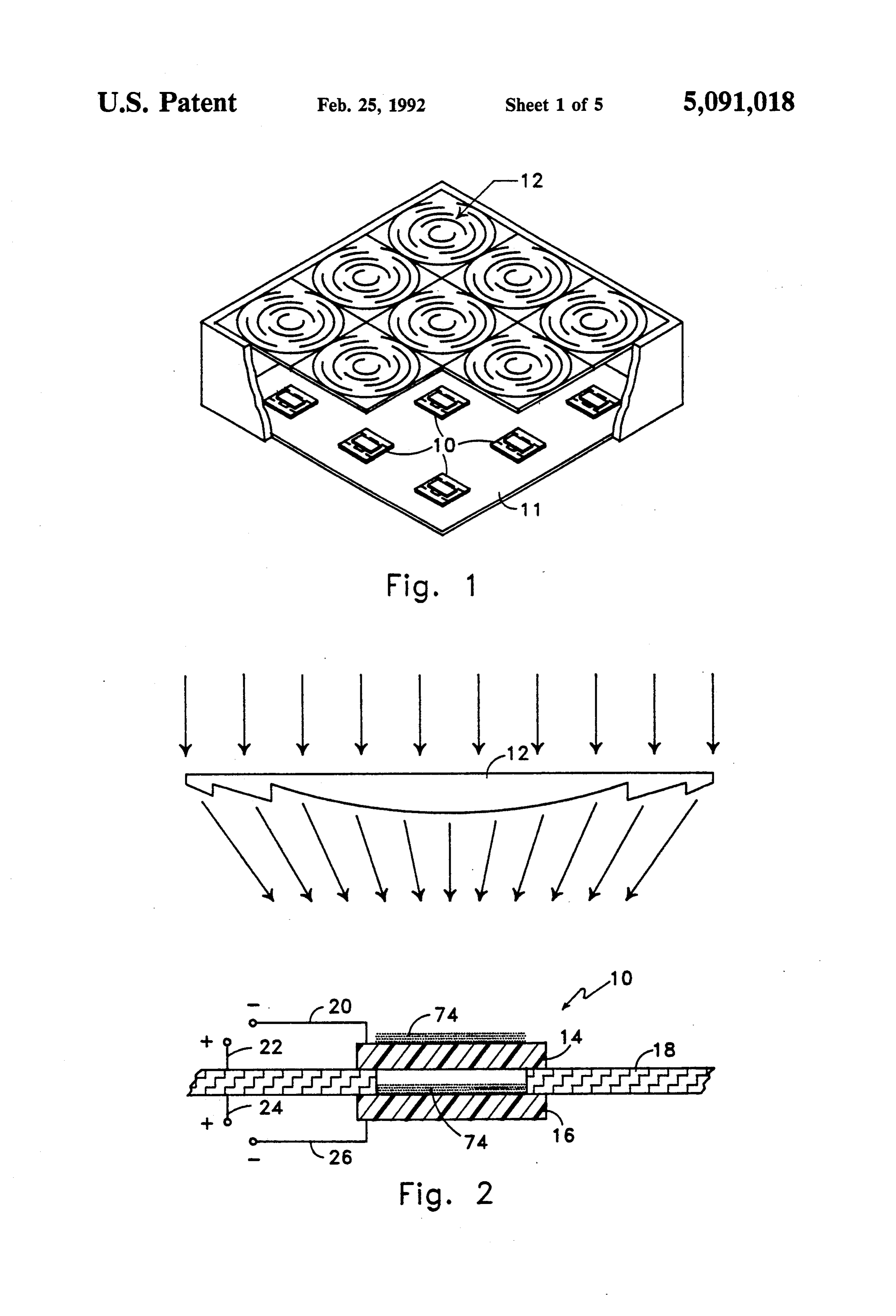
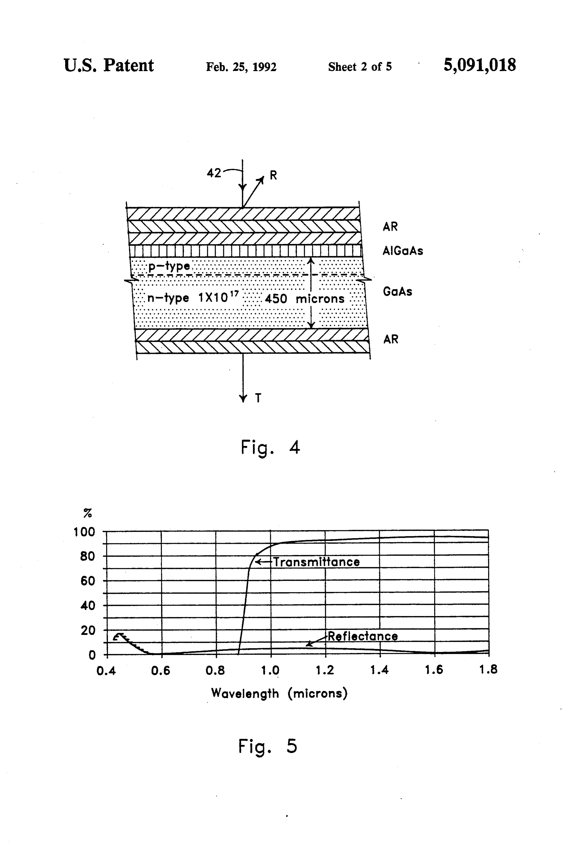
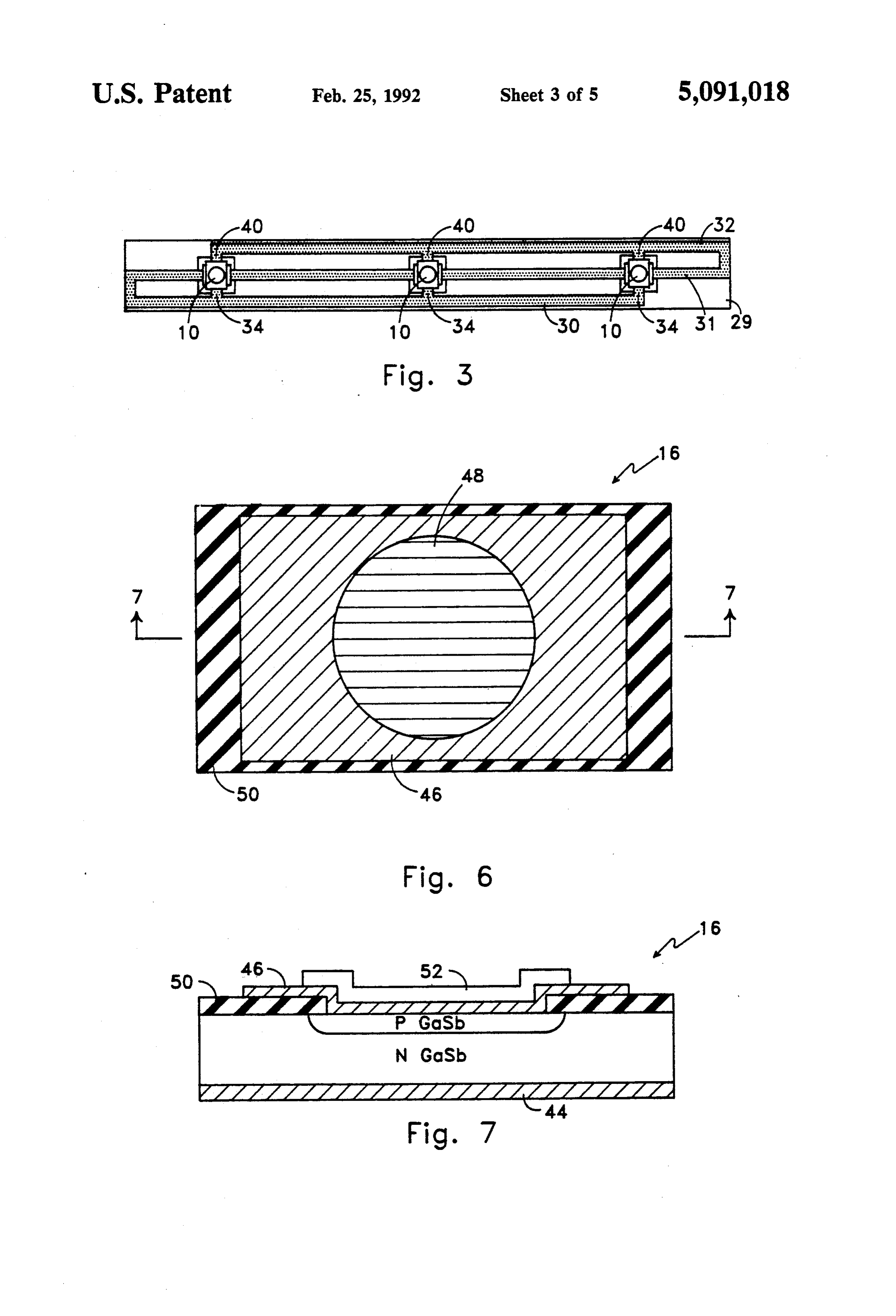
FIG. 1 is a pictorial view of a multi-cell solar energy Card 18 may be a sapphire layer that serves also as a array embodying a preferred embodiment of the present heat sink or spreader. Al2O3 and AlN materials are invention; suitable as a support between the upper and lower cells, FIG. 2 is a diagrammatic view of a single cell of the 10 because they have electrical insulating and thermal array of FIG. 1; conducting properties.
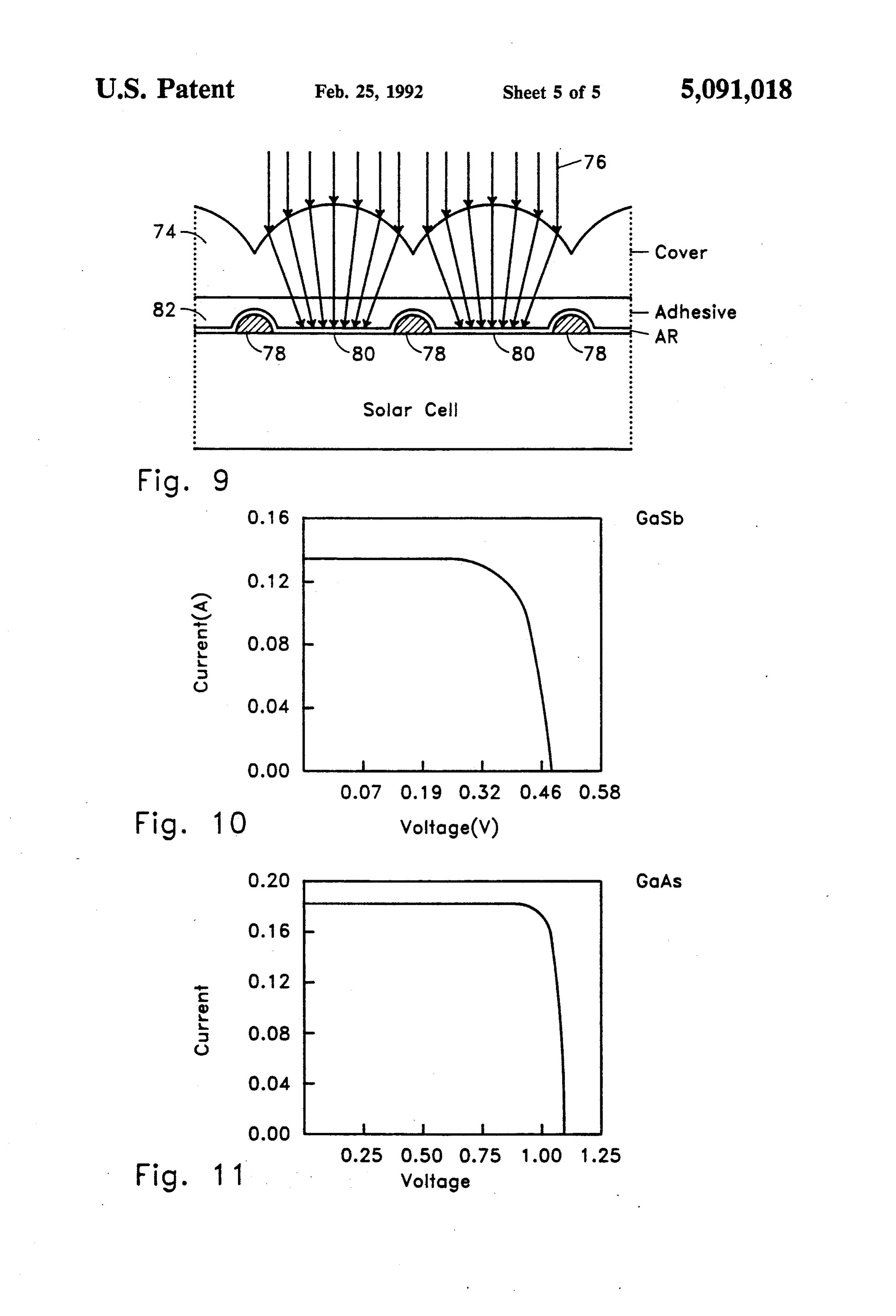
FIG. 3 is a view of a circuit ribbon that may be used An alternative interconnect between adjacent cells for connecting the four terminals of a tandem cell unit for terrestrial installations may be provided by a flex to provide a two-terminal device; circuit ribbon 29 as shown in FIG. 3 which comprises FIG. 4 is an elevation in cross section of the upper 15 electrical conductors on a suitable synthetic resin mate cell of a tandem cell unit; rial. Three elongated flexible strips 30,3132 of conduc FIG. 5 is a curve showing the optical transparency tive material extend along the length of ribbon 29. The properties of a gallium arsenide photovoltaic cell as strip 30 is formed with a flap 34 that may engage the shown in FIG. 4; metallized surface that is on the upper surface of upper FIG. 6 is a top view of the lower cell of a tandem cell 20 cell 14. The strip 32 is formed with a flap 40 that serves unit; as an electrical connection to the lower surface of the FIG. 7 is a elevation in cross section of the lower cell upper cell 14. The strip 31 is connected electrically to taken along lines 7-7 of FIG. 6; the upper and lower surfaces of the lower cell 16 so that FIG. 8A-8E are process flow diagrams outlining the all three lower cells 16 are connected electrically in novel process for fabricating a III-V booster solar cell 25 series. The upper cells are connected electrically in in accord with one feature of the present invention; parallel. Where the upper cell open circuit voltage is FIG. 9 is an elevation to a large scale showing a approximately three times the open circuit voltage of prismatic lens which optically eliminates grid line ob the lower cell, this series and parallel connection system scuration losses for the solar cells; allows the cells to be connected together to give a two FIG. 10 is a curve showing current vs. voltage for an 30 terminal device. It may be noted from FIGS. 10 and 11 illuminated GaSb cell; and that a GaAs cell has a maximum power voltage of 971 FIG. 11 is a curve showing current vs. voltage for an mV which is slightly less than the maximum power illuminated GaAs cell. voltage for three series connected GaSb cells where DESCRIPTION OF PREFERRED each has a corresponding voltage of 380 mV.
EMBODIMENTS GaAs Cell
Referring to FIG. 1, the sunlight concentrating pho Conventional GaAs cells must be made transparent to tovoltaic array of the present invention is illustrated by achieve the highest conversion efficiency in a tandem or an arrangement of nine solar cell units 10 in a housing 11 stacked cell application. Several methods of forming which includes also a concentrating lens 12 which has GaAs photovoltaic cells are known in the art as ex nine focal regions, one for each cell. Each of the solar plained in the McLeod et al U.S. Pat. No. 4,776,893. cell units 10 is substantially equidistant from its respec Further recent developments are reported in an article tive concentrating lens 12. "Tertiary Butyl Arsine Grown GaAs Solar Cell' by Each solar cell unit 10 may be of a type illustrated in Sundaram et al, Appl. Phys. Lett. 54 (7), Feb. 13, 1989, FIG. 2, and positioned in optical alignment with its 45 where growing p- and n-doped GaAs layers and p portion of the concentrating lens. The cell unit 10 is AlGaAs layers for use as a concentrator solar cell struc shown to be formed of two cells, one being an upper ture is described. See also Fan et al, U.S. Pat. No. cell 14 and the other being a lower cell 16. The cells 14, 4,547,622.
16 are mechanically separate so that during manufac Three modifications to such GaAs cells are made ture, an upper cell 14 may be selected for use with one 50 when used with GaSb lower cells to optimize the con of a group of lower cells 16. The cells 14,16 may have version efficiency. First, the conventional continuous an active surface area of 0.049 cm2, although it should back metallization should be replaced with a gridded be understood that areas of other sizes are also useful. metallization. The back grid should use fewer grid liens The upper cell 14 is ideally transparent to the radiation than the front grid because the thicker wafer conductiv to which the lower cell has sensitivity. 55 ity is much higher than the thinner emitter conductiv The cells 14, 16 may be separated by a space which ity. The shading from the back grid may be omitted allows separate electrical terminals to be provided for entirely.
the lower surface of the upper cell 14 and the upper Second, the water n-dopant density of the GaAs surface of the lower cell 16. The cells 14,16 may be material should be reduced from 1 x 101 cm-3 to about mounted over holes in a ceramic-double sided printed 1x1017 cm-3 to reduce free electron absorption. wiring card 18 which is supported at an index position Third, the anti-reflective (AR) coatings on the front on the housing 11 thereby to serve as part of the array and back of the GaAs cell are modified in order to structure. The upper cells 14 are mounted on the front provide minimal reflection across a broader bandwidth side of card 18 and the lower cells 16 of the tandem to assure passage of longer wavelength energy to which arrangement are mounted on the back side of the same 65 the GaSb cells are responsive.
card 18 to be an optical alignment with its associated The presently preferred transparent GaAs cell design upper cell. Other mounting arrangements for the cells incorporates a 450 micrometer (micron) thick n-type may be used. wafer doped to about 1x1017 cm-3 with complete
Page 9
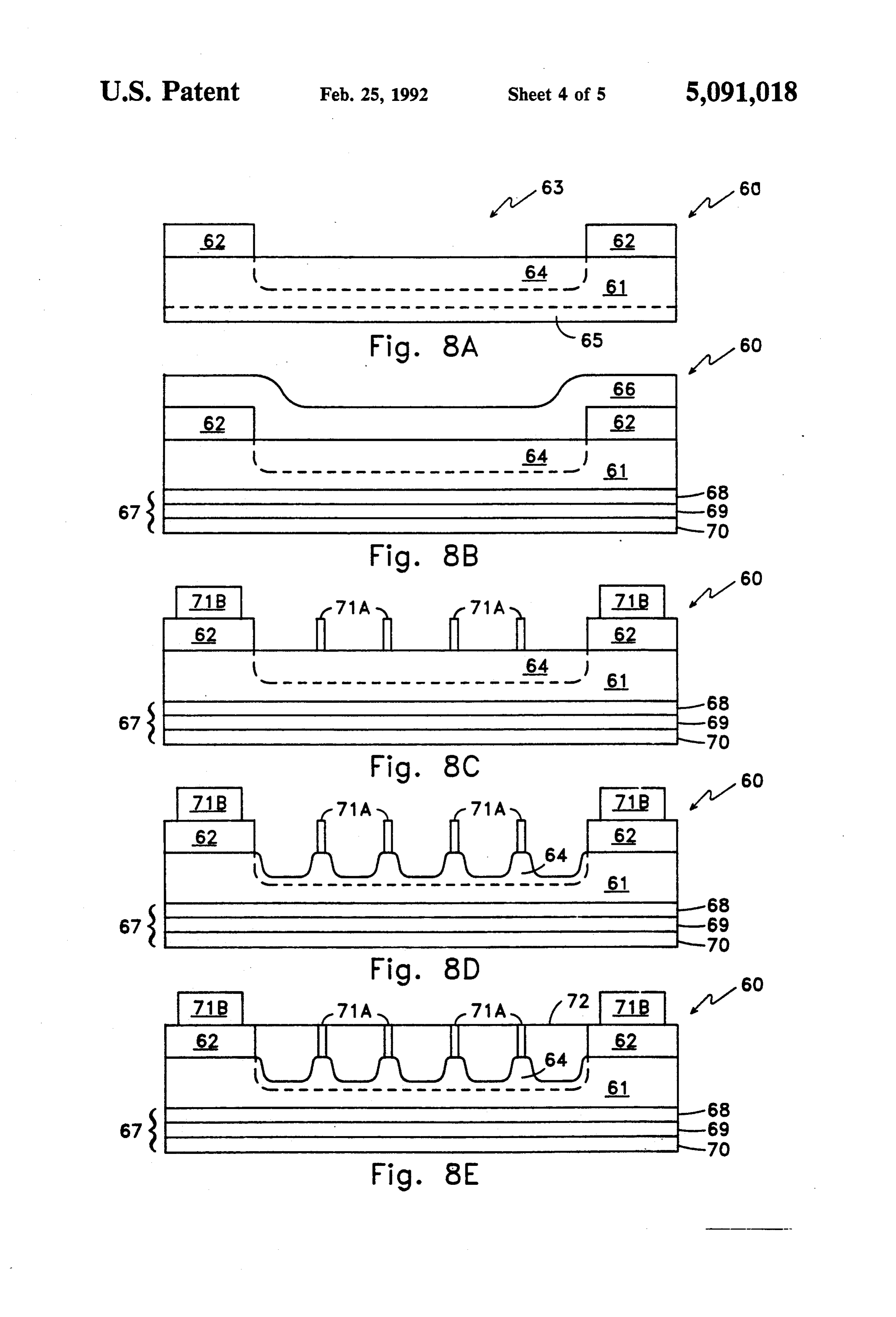
photovoltaic epitaxial structure grown on it including a preferred form, but instead advantageously may use an AlGaAs window layer. A three layer AR coating on an n-type GaSb wafer with a p-dopant, such as zinc, the front surface in addition to the AlGaAs window that is added by a less costly diffusion process. layer serves as the front side AR coating and a two The cell shown in FIG. 7, has a metallized base 44 layer AR coating has been applied to the back side in which may be connected to the terminal 26 of FIG. 2. some embodiments. Important design parameters in The bus conductor layer 46 is an upper metallized clude the thickness and refractive index of each layer surface which may be connected to the terminal 24 of including the AlGaAs which functions not only as an FIG. 2. Two important aspects are that only the grid electronic heteroface but also as one of the front AR lines 48 are in contact with the semiconductor at the layers. This multi-layer optical system produces a very 10 zinc diffused region designated P GaSb in FIG. 8 and broadband reflectance minimization through the visible the bus conductor layer 46 must be isolated from the energy range on out beyond the GaSb band edge at GaSb semiconductor substrate. Because the process is 1700 nm as illustrated in FIG. 5. essentially planar, the front side metallization is on an The GaAs cells and the GaSb cells may be of the insulation mask 50 of an insulative material such as same size. The chip size may be 3 mmX5 mm and the 15 silicon nitride. The anti-reflective coating 52 is impor cell active area diameter may be 2.5 mm. Nineteen grid tant in achieving efficient energy conversion but is not lines traverse the front active area of each such cell. The essential to operability of the solar cell. grid density is similar to that used with a GaAs cell The process for fabrication of the GaSbbooster cell is designed for 20X sunlight concentration. For an n-type generally applicable to III-V diffused junction photo GaAs wafer doping density of 1 x 1017 cm-3 and for a 20 voltaic cells. The reference to the specific gallium anti 20X sunlight concentration, it appears that no grid monide material is therefore to be construed as illustra lines are required on the back side of the GaAs cell. tive and not limiting. The process will be described with FIG. 4 shows a cross section of one preferred GaAs reference to FIGS. 8A-8E.
solar cell that is adapted for use as part of the present Preferably, substrate 61 is composed of a III-V com invention. The solar energy along line 42 is directed 25 pound semiconductor material single crystal. The use of toward the GaAs cell with a part being reflected along an n-type substrate with a room temperature carrier line R and a part being transmitted along line T. With concentration of approximately 1017 atoms/cm3 is pre anti-reflective coating layers AR on both the front and ferred and results in good device performance without back sides of the GaAs cell, the relative transmittance a surface passivation layer. At lower doping levels, the and reflectance can be made to have values indicated by 30 surface of the n-type GaSb converts to p-type to an F.G. 5. extent that degrades device performance. At higher The upper AR layer includes the AlGaAs layer doping levels, excessive tunneling through a junction which may specifically be Alo.5Gao.5As and about 0.05 degrades device performance. In one embodiment, the microns thick to reflect free electrons toward the p-n GaSb wafer may be doped with Te to 4x10¹⁷/cm3. junction in this cell. Three additional layers have been 35 Zinc is a preferred p-type dopant material. found effective to enhance the anti-reflective proper An insulating layer 62 is then formed as a coating on ties. Materials such as Ta2O5, MgO, MgF, Tio and the upper surface of substrate 61. Insulative layer 62 is SiO2 are materials that have been found effective. The preferably a two-layer coating of silicon nitride/silicon thickness of each layer is but a fraction of the wave oxynitride. This two-layer system has been used in fab length of the visible portion of the spectrum. 40 ricating gallium arsenide lasers, and has been discov For optimum anti-reflective properties, the AR layer ered here to be also effective for use in the method of on the back side may require two equally thin layers of the present invention. The first layer comprising silicon TiO, and SiO2. Deposition by electron beam evapora nitride is utilized to minimize any oxygen contact with tion at room temperature may be used for applying substrate 61. The second layer comprising silicon oxyni these layers. 45 tride is much more stable and holds up to the high tem The electrical conducting grid pattern on the upper perature excursion of a subsequent diffusion step. The surface of the cell of FIG. 4 may consist of the usual two-layer insulating layer may be deposited using parallel conductors applied by conventional photolitho plasma chemical vapor deposition. The first layer of graphic techniques. Pt/Au and Au/Ge/Ni/Au layers silicon nitride may be about 0.01 microns thick and the that are electron beam evaporated and appropriately 50 second layer of silicon oxynitride approximately 0.1 heat treated to make p and n ohmic contacts on the microns to perform effectively. Insulating layer 62 may front and back sides, respectively, may be used. also be applied by sputtering. Because electrical conductivity of the n-type GaAs Insulating layer 62 is next treated to form opening 63 material is good, the back electrode may be made with exposing a portion of substrate 61 as by using standard fewer conductors and larger spacings between conduc 55 photolithography techniques. Thus, a layer of photore tors. To provide maximum transparency properties to sist may be deposited in a patterned form on the insulat the upper GaAs cell, the electrical conductors on the ing layer 62. Thereafter the photoresist is developed to base surface may be omitted in cases where cell areas remove the insulating layer 62 at the opening 63. A are small. p-type dopant material, such as zinc, is then diffused GaSb Cell into the exposed surface of substrate 61 to serve as a conductivity type modifier and form a p?njunction and
FIGS. 6 and 7 diagrammatically illustrate the lower p-type emitter 64.
cell which is preferably made of GaSb. In the prior art The diffusion step may be accomplished using a McLeod U.S. Pat. No. 4,776,893, the GaSb solar cell quasi-closed graphite box, not shown, in a conventional included the use of an AlGaSb window layer. Fabrica 65 manner. The box has an elemental zinc source and an tion was by a liquid-phase epitaxy method. The photo elemental antimony source. The elemental Sb source is voltaic GaSb cell used in the tandem cell of the present provided to build up the antimony pressure in the diffu invention does not employ the AlGaSb window layer in sion chamber to prevent portions of the antimony in
Page 10
substrate 61 from exiting substrate 61. The elemental Zn ing 22 is tantalum pentoxide (Ta2O5) having a thickness provides a source of p-type dopant atoms which diffuse of approximately 0.15 microns which was found to raise through opening 63 into the lattice substrate 61. The the short circuit current by another 1.5 times. concentration versus depth into substrate 61 of the Zn A prismatic cover-glass 74 which optically eliminates dopant atoms is a function of time and temperature. The grid line obscuration losses for concentrator cells is diffusion step preferably creates an emitter doped in the shown in FIG. 2, and on an enlarged scale in FIG. 9. mid-100/cm3 range to a depth of approximately 0.5 Incoming light rays 76 that otherwise might hit parallel micrometers (microns). During the diffusion process, an grid lines 78 are simply bent slightly toward active cell unwanted zinc diffused region 65 forms on the back side areas 80 as they enter the thin molded cover 74 which of the substrate 61 as illustrated in FIG. 8A. 10 may have the form of a cylindrical lens and be made of Following the diffusion step, a protective photoresist a synthetic resin material.
layer 66 is deposited on the surface of substrate 61 to FIG. 9 shows the cover-glass 74 as it is applied by an form a patterned insulating layer 62 as shown in FIG. adhesive 82 to both the GaAs and GaSb cells to boost 8B. The back side or lower surface of substrate 61 is the light generated currents and efficiencies of both thereafter non-selectively etched to remove unwanted 15 cells 14,16. The observed gain in the GaAs cell current zinc that has diffused into region 65. Protective photo is near 10%. Since the GaSb cell in the FIG. 2 configu resist layer 66 is removed and a back side metallization ration is shaded by both the GaSb grid lines and the contact layer 67 is formed. GaAs cell grid lines, the current increase for the GaSb Metallization contact layer 67 must have low electri cell is more than 10%. For assembled GaAs/GaSb cal resistance, be adherent to the lower surface of sub 20 tandem stacks the two cells are preferably mounted strate 61 and meet the qualifications for use in space or with their respective grid lines perpendicular to each terrestial applications. A typical example may comprise other. The two sets of cylindrical lenses in the two prismatic covers are cross linear and such an arrange three layers of metal: a layer of titanium (Ti) 68, a layer of palladium (Pd) 69, and a layer of gold (Au)70. Plati ment contributes to the high energy conversion levels num (Pt) would also be an acceptable alternative to 25 that have been obtained.
palladium 69. Gold 70 is used because of its good elec FIG. 10 shows performance data for an individual trical properties. Palladium 69 is used as a gold diffusion GaSb cell with a cover 74 as described in connection barrier to make contact between titanium 68 and gold with FIG. 9 and broadband anti-reflective coatings as 20 and to prevent gold 20 from diffusing into titanium described and tested behind a GaAs radiation filter. The 68 or substrate 61, FIG. 8B. The back side metal layers 30 cell has an illuminated current versus voltage as illus may be alloyed in a furnace. trated and fill factor of 7.3%. The open circuit voltage A second photolithographic step is used to form the is 480 mV. The illuminated short circuit current density grid pattern for a top metal 71. Top metal 71 consists of is 2702 mA/cm2. Boost efficiencies are 8.2% for space a grid portion of parallel lines 71A of conductive mate application where air mass effects are 0 (AMO) and rial and a bus portion 71B of conductive material as 35 9.3% where air mass density is 1.5 directed (AM 1.5D). illustrated in FIG. 8C. Top metal 71 may comprise a Concentrated light intensities of near 100 suns equiva layer of Pt and a layer of Au, Top metal 71 including lent were used.
grid lines 71A and bus portion 71B is formed using FIG. 11 shows similar data for an individual GaAs standard metal liftoff techniques. In actual processing, cell with a prismatic cover 74 as described in connec the thickness of metal layer 71 may be approximately tion with FIG. 10 and anti-reflective coatings as de 0.3 microns. Only the grid lines touch the junction re scribed above. The curve shows illuminated current gion. The bus pad is deposited only on the patterned versus voltage. The open circuit voltage is 1100 mV and insulative material and is isolated from the n-type semi the fill factor is 0.85. The illuminated short circuit cur conductor substrate. rent density is 3472 mA/cm2. Energy conversion effi A front side etch is then performed to reduce the 45 ciencies are 24.1% (AMO) and 28.9% (AM 1.5 D) at a emitter thickness. This is illustrated in FIG. 8D but the light concentration near 100 suns equivalent. drawing is not to scale. It should be noted that while the Theoretical tandem cell stack efficiencies sum to front side etch is not necessary, it has been found that 9.3%-28.9% = 38.2 at AM 1.5 D. This conversion with removal of emitter material to provide a recess efficiency translates to 8.2% +24.1% =32.3% for space between grid lines 71A beneficial results are obtained. 50 (AMO). Several tandem cell stacks actually have been For example, if the depth of the recess is sufficient so fabricated with AMO energy conversion efficiencies of that the emitter material thickness is reduced from at least 31% and with AM 1.5 D energy conversion about 0.5 micrometers to about 0.1 micrometers, the efficiencies of between 34% and 37%. The higher effi device short circuit current rises by a factor of about 2. 55 ciencies are achieved with the best cells used. It is apparent that the depth of the zinc diffusion is While preferred embodiments have been shown and variable with the depth under the conductive strips 71A described, those skilled in the art will readily recognize being greater than the depth between the strips. alterations, variations, or modifications that might be An anti-reflective coating 72 may be deposited as a made to the particular embodiments that have described coating over the emitter between the grid lines 71A as without departing from the inventive concept. This illustrated in FIG. 8E. FIG. 8E, like FIG. 8D, is dia 60 description and the drawings are intended to illustrate grammatic and not to scale. Anti-reflective coating 22 the invention (and its preferred embodiments), and are may comprise a single layer or double layers and is not meant to limit the invention.
often deposited using a vacuum deposition process as We claim:
discussed in conjunction with the upper GaAs layer 1. A method for improving the energy conversion fabrication. It should be apparent to those skilled in the 65 efficiency of a GaAs/GaSb tandem solar cell, compris art that anti-reflective coating 22 should be tailored ing the step of using a diffused junction GaSb cell. specifically for a spectral region of interest for booster 2. A GaAs/GaSb tandem solar cell having improved cell. One preferred embodiment of anti-reflective coat conversion efficiency, comprising:
Page 11
(a) a GaAs upper cell having a predetermined band 12. A solar cell array comprising: gap selected for optimal performance of the tan a solar energy collector;
dem solar cell; a plurality of solar cell units positioned with respect (b) a GaSb booster cell positioned beneath the GaAs to one another and with respect to a solar energy upper cell to receive light transmitted through the 5 collector;
GaAs upper cell and responsive to such light; and a first group of cells made of GaAs and a second (c) light conditioning means associated with the group of cells made of GaSb that are each mechani upper cell and the booster cell for achieving an cally stacked relative to and physically separate energy conversion efficiency of at least 31% AMO. from a corresponding one of the GaAs cells of the 3. The cell as defined in claim 2, wherein the light O first group;
conditioning means includes a prismatic coverglass for said GaAs cells having on an upper surface nearest optically eliminating grid line obscuration losses on at said collector a multiple layer of different materials least said upper cell and a concentrating lens for focus to form an upper anti-reflective coating that passes ing solar energy onto an upper surface of said upper solar energy having wavelengths longer than cell. 15 wavelengths of energy absorbed by GaAs in addi 4. The cell as defined in claim3, further having multi tion to one layer that also serves to reflect free ple layers of anti-reflective materials on each of oppo electrons toward a p-n junction in said GaAs cell; site surfaces of said upper cell. parallel conductors on the upper surface of the GaAs 5. A tandem solar cell unit for efficient conversion of solar energy into electrical energy comprising: cells which are connected to a first cell terminal; electrical contact means on the lower surface of the .
an upper solar cell that is transparent to radiation GaAs cells which are connected to a second cell energy at a wavelength longer than the wavelength terminal;
to which said upper cell is sensitive, said upper cell said GaSb cells having a p-type diffusion layer and a having parallel grid lines of conductive material on radiation receiving area, said radiation receiving
area having parallel conductors on an upper sur a lower solar cell sensitive to said longer wavelength face contacting the diffusion layer in each GaSb energy mounted in optical alignment with said cell, said parallel conductors being connected to a upper cell to receive said longer wavelength en third cell terminal that is electrical isolated from ergy, said lower cell having parallel grid lines of conductive material on an upper surface thereof; 30 saidsaidGaSb second cell terminal;
cells having a metallized lower surface multiple anti-reflective layers of different materials connected to a fourth cell terminal. on an upper surface of said upper cell;
multiple anti-reflective layers of different materials 13. The array as defined in claim 12, wherein the positioned between the upper and lower cells; and GaAs cell of each cell pair is in optical alignment with means for optically eliminating grid line obscuration 35 the GaSb cell of the same cell pair and physically losses on at least said upper cell. spaced so that the facing lower surface of the GaAs cell 6. The solar cell unit as defined in claim 5, wherein is electrically isolated from the facing upper surface of the GaSb cell.
the lower cell is made of GaSb semiconductor material with n-type conductivity having said upper surface 14. The array as defined in claim 13, wherein said coated with an insulating layer which has an aperture plurality of cell pairs are arranged in rows and columns that serves as a mask opening for diffusion of a p-type to be substantially equidistant from said collector, there emitter dopant into said semiconductor under the aper being layers of different materials to form a second ture but not under the insulating layer; and lower anti-reflective coating located between the said upper surface has a bus conductor overlying said stacked cells.
insulative layer and electrically connected to said 45 15. The array as defined in claim 14, wherein the grid lines which extend across a p-type doped layer physical spacing between the facing surfaces of the surface so that the bus conductor is electrically GaAs and GaSb cells is provided by a printed circuit isolated from said semiconductor. board which has conductors on opposite sides that are 7. The solar cell unit as defined in claim 6, wherein connected to said second and third terminals. the diffused p-type doped layer has a depth of approxi 50 16. The array as defined in claim 14, having a pris mately 0.5 micrometer, the grid lines are deposited on a matic cell cover-glass associated with the upper cell surface of said p-type doped layer and the emitter depth which reduces obscuration losses due to said parallel between the grid lines is sufficiently small to cause the conductors on the upper GaAs surface. short circuit current to rise. 17. The array as defined in claim 16, wherein a second 8. The solar cell unit as defined in claim 7, wherein 55 prismatic cell cover-glass is associated with the GaSb the doped layer between the grid lines contains an anti cell, said prismatic cell cover-glass being shaped and reflective coating that is effective to further increase the oriented to reduce obscuration losses of the parallel short circuit current. conductors on the upper GaSb surface. 9. The solar cell unit as defined in claim 8, wherein 18. The array as defined in claim 12, wherein the the anti-reflective layer on the doped layer includes electrical contact means on the lower surface of the tantalum pentoxide. GaAs cells is configured to provide maximum transpar 10. The solar cell unit as defined in claim 5, wherein ency to the wavelength spectrum to which the GaSb the upper cell is made of GaAs with an n-type dopant cell is responsive.
density to reduce free electron absorption, said upper 19. The array as defined in claim 24, further having cell having fewer grid lines on its lower surface than on on the lower surface of the GaAs cells layers of differ the upper surface. ent materials to form a lower anti-reflective coating. 11. The solar cell unit as defined in claim 5, further 20. The array as defined in claim 12, further having comprising a solar concentrating means. on a lower surface of the GaAs cells that is remote from
Page 12
said solar energy collector layers of different materials 28. The solar cell as defined in claim 21, wherein the to form a lower anti-reflective coating. means to enhance anti-reflective properties further in 21. A tandem solar cell unit that is adapted for use clude layers on the lower surface of the upper solar cell. with a solar energy collector and comprises: 29. An array of tandem solar cell units in a housing an upper solar cell that is transparent to radiation 5 comprising:
energy at a wavelength longer than the wavelength rows and columns of discrete solar cell units includ to which said upper cell is sensitive and a lower ing an upper cell having a first pair of terminals, a solar cell comprising a diffused junction GaSb lower cell mounted in optical alignment with and layer substrate, said cells being in optical alignment beneath a corresponding upper cell, said lower cell so that substantially all radiation energy that passes 10 having a second pair of terminals; through the upper cell is received by the lower a support member of electrically insulating thermally cell; conducting material anchored to said housing and means to enhance anti-reflective properties for the contacting the lower side of the upper cell and the wavelengths of energy to which both solar cells are upper side of the lower cell said support member responsive including a plurality of thin layers of having an aperture optically aligned with the said different materials on an upper surface of said upper and lower cells for transmission of solar upper solar cell; energy between the upper cell to the lower cell; conductive material on an upper surface of each cell electrical conductors carried by said support member that is connected to respective first and second 20 which provide electrical current paths between the electrical terminals; upper and lower surfaces of the upper and lower the lower surface of the upper cell having electrical cells and said first and second pairs of terminals; current conductive properties and being connected said lower cell being a III-V n-type semiconductor which has:
to a third electrical terminal; and a layer of electrical insulating material that has a the lower surface of the lower cell having a metal 25 central opening on an upper surface of said lized layer connected to a fourth electrical termi lower cell;
nal.
22. The solar cell as defined in claim 21, wherein the a p-type dopant material diffused in the upper sur conductive material on the upper surface of the upper face through said central opening to form a diffu cell is in the form of parallel conductors that are posi 30 sion layer; and tioned to be between said upper cell upper surface and conductive material on the cell upper surface a prismatic cover-glass that is shaped to reduce obscura which comprises a plurality of parallel conduc tion losses due to said parallel conductors. tors that are on the diffusion layer and a bus portion that is on top of said insulating material, 23. The solar cell as defined in claim 22, wherein the said bus portion providing an electrical current conductive material on the upper surface of the lower is path between said parallel conductors on the cell is in the form of parallel conductors that are be diffusion layer and one of said electrical conduc tween the p-type diffusion layer and a second prismatic tors carried by said support member; cover-glass that is shaped to reduce obscuration losses a solar energy concentrating element associated with due to the parallel conductors on said lower cell. each solar cell unit; and 24. The solar cell as defined in claim 21, wherein the 40 a first anti-reflective material on the upper surface of upper surface of the lower solar cell substrate contains an upper cell and a second anti-reflective material a layer of electrical insulating material that has a central between the lower surface of the upper cell and the opening; upper surface of the lower cell. said p-type diffusion layer on the upper substrate 30. The solar cell array as defined in claim 29, surface is within said opening; 45 wherein an upper surface portion of the diffusion layer the conductive material on the upper surface of the that is located between said parallel conductors is re lower solar cell substrate comprises a plurality of moved to form surface depressions to increase short conductors on the diffusion layer and a bus portion circuit current and an anti-reflective coating material is that is on top of said insulating material layer, said applied in said depressions between the parallel conduc bus portion providing an electrical current path 50 tors.
between said parallel conductors on the diffusion 31. The solar cell array in claim 30, further compris layer and one of said terminals. ing a prismatic cover-glass which optically eliminates 25. The solar cell as defined in claim 24, wherein an grid line obscuration losses having a lower surface that upper surface portion of said diffusion layer that is lo is adhered to the top surface of the lower solar cell. cated between said parallel conductors contains depres 55 32. The solar cell array as defined in claim 31, sions formed by removal of an amount of said diffusion wherein the upper cell has an upper surface having layer that is sufficient to increase the short circuit cur conductive material in the form of parallel conductors rent of the lower solar cell. that are positioned so as to be optically covered by a 26. The solar cell as defined in claim 25, further com prismatic cover-glass, said cover-glass being shaped to prising an anti-reflective coating material applied in said 60 reduce obscuration losses in said upper cell due to said depressions between said parallel conductors that is parallel conductors.
effective to further increase the short circuit current of 33. A method for producing a solar cell comprising the lower solar cell. the steps of:
27. The solar cell as defined in claim 26, wherein the providing a GaSb substrate of n conductivity type; anti-reflective, current enhancing means comprises at 65 depositing an insulating layer on a first surface of said least two layers of different anti-reflective materials substrate;
between the lower surface of said upper solar cell and depositing a layer of photoresist on said insulating the upper surface of the lower cell. layer;
Page 13
developing said photoresist to form an opening there depositing a layer of photoresist on said insulating through and to expose a portion of said insulating layer;
layer; removing the photoresist to define the grid lines in etching said exposed portion of said insulating layer the originally uncovered portion and the bus; to expose a portion of said substrate; 5 depositing metal over the photo-patterned cell; and diffusing a p-type dopant into said exposed portion of removing the remaining photoresist and metal depos said substrate to form a p-type diffused area; ited on the photoresist while leaving the grid lines and bus.
depositing a protective material on said diffused area; 40. The method of claim 37, wherein the steps of non-selectively etching a second surface of said sub 10 forming said grid and said bus are performed in a single strate to remove any unwanted p-type dopant; operation.
depositing a contact metal layer on said second sur 41. The product of the method of claim 40. face of said substrate; 42. The product formed by the method of claim 37. depositing a layer of photoresist on the first surface of 43. In a tandem solar cell having a front solar cell said substrate; 5 through which radiation passes to a booster solar cell, exposing said photoresist to define a grid opening and said booster cell comprising:
a bus opening therethrough; an n-type GaSb material having a zinc diffused region developing said photoresist to form openings there being free of an AlGaSb window layer for surface through which expose portions of said diffused and passivation on a portion of a first surface of the non-diffused areas of said substrate first surface; 20 GaSb, said first surface being mounted to receive depositing a metal on said photoresist and in said radiation passing through said front solar cell and openings defined therethrough; having a marginal edge covered with an insulating removing said photoresist and said metal deposited layer;
thereon; and a back metal contact adhered to a second surface of etching non-metallized portions of said diffused area 25 the GaSb; and of said substrate by an amount sufficient to increase metallization on said first surface including a layer of short circuit current of the celi. conducting material extending over at least a por 34. The method of claim 33, wherein said p-type tion of said insulating layer and patterned to pro diffused area comprises zinc doped in a mid-1020/cm3 30 vide grid lines formed to pass solar energy into said range to a depth of approximately 0.5 micrometers. zinc diffused region and contacting said zinc dif 35. The method of claim 34, wherein the method fused region for providing a low resistance electric further comprises etching non-metallized portions of current path to an edge surface of the metallization that is supported on said insulating layer and out of said diffused area by a depth of about 0.4 micrometers contact with the GaSb material. to form recesses between the metallized portions, and 35 44. The solar cell of claim 43 wherein said grid lines depositing a layer of anti-reflective material in said are in the form of parallel strips of conductive material recesses, and the thickness of the zinc diffused region is variable 36. The method of claim 33 wherein the insulating with the thickness under the strips being greater than layer comprises a thin silicon nitride layer in contact the thickness between the strips. with said substrate and a thicker overlying silicon oxy 45. The solar cell of claim 43 wherein said insulating nitride layer. layer comprises a first layer of silicon nitride and a 37. A method for producing a solar cell, comprising second layer of silicon oxynitride.
the steps of: 46. The solar cell of claim 43 wherein the front solar providing a body of n-type GaSb material including cell is made of GaAs that is transparent to radiation to on one surface a covered portion defined by a 45 which the booster solar cell is responsive and formed with metallization that minimizes shadowing of the lower of insulating material over the GaSb and at booster least one uncovered portion; cell.
diffusing a p-type dopant into the GaSb through said energy47. A method of converting solar energy to electrical uncovered portion to form a p-n junction near said 50 sunlight,bysaid exposing a tandern solar cell to concentrated tandem cell being comprised of an upper surface; GaAs solar cell facing said sunlight and a lower diffused metallizing said surface by depositing a layer of con junction GaSb solar cell.
ductive material on the GaSb on the uncovered 48. The method of claim 47 wherein the GaSb cell is portion to form grid lines and on the covered por free of any upper, passivating, epitaxial overcoat. tion of insulating material to form a bus. 55 49. A solar concentrator module comprising a tan 38. The method of claim 37 further including the step dem solar cell comprised of an upper GaAs solar cell of attaching external electrical circuit connections to and a lower diffused junction GaSb solar cell; and a the bus. solar concentrating means for focusing and concentrat 39. The method of claim 37 wherein the step of metal. ing incident light upon the tandem solar cell.
Provenance
- Collection
- Cited prior art
- Original PDF
- patentimages.storage.googleapis.com →
- Filed
- 1990-05-14
- Pages
- 13
- Method
- pdftotext (the PDF's own text layer) + pdftoppm 300dpi page scans
- Source
- Google Patents bibliographic record
- Granted
- 1992-02-25
- Inventors
- Lewis M. Fraas; James E. Avery; Gerald R. Girard; Boeing Co
- Transcribed from
- patentimages.storage.googleapis.com →