patent · US20090250096A1
Solar-To-Electricity Conversion Sub-Module
8 October 2009
Page 1 — bibliographic record
(19) United States (12) Patent Application Publication (10) Pub. No.: US 2009/0250.096 A1
Pan (43) Pub. Date: Oct. 8, 2009 (54) SOLAR-TO-ELECTRICITY CONVERSION Related U.S. Application Data SUB-MODULE (60) Provisional application No. 61/043,014, filed on Apr.
(76) Inventor: Eric Ting-Shan Pan, Fremont, CA Publication Classification
Correspondence Address: (52) U.S. Cl. ......................................... 136/248: 136/246 J. NICHOLAS GROSS, ATTORNEY (57) ABSTRACT 2030 ADDISON ST, SUITE 610 The invention addresses the area utilization and capital effi BERKELEY, CA 94704 (US) ciency of systems for converting Solar energy into electricity. A solid-state solar submodule includes photovoltaic and ther moelectric or thermionic cells. The submodule can be imple mented in various configurations and by a solar insolation (21) Appl. No.: 12/417,931 flux collection and concentration method to improve the area utilization and Solar-to-electricity conversion efficiency. A thermal expansion matched multilayer board is also used to (22) Filed: Apr. 3, 2009 withstand ultra high concentration of Solar insolation flux.
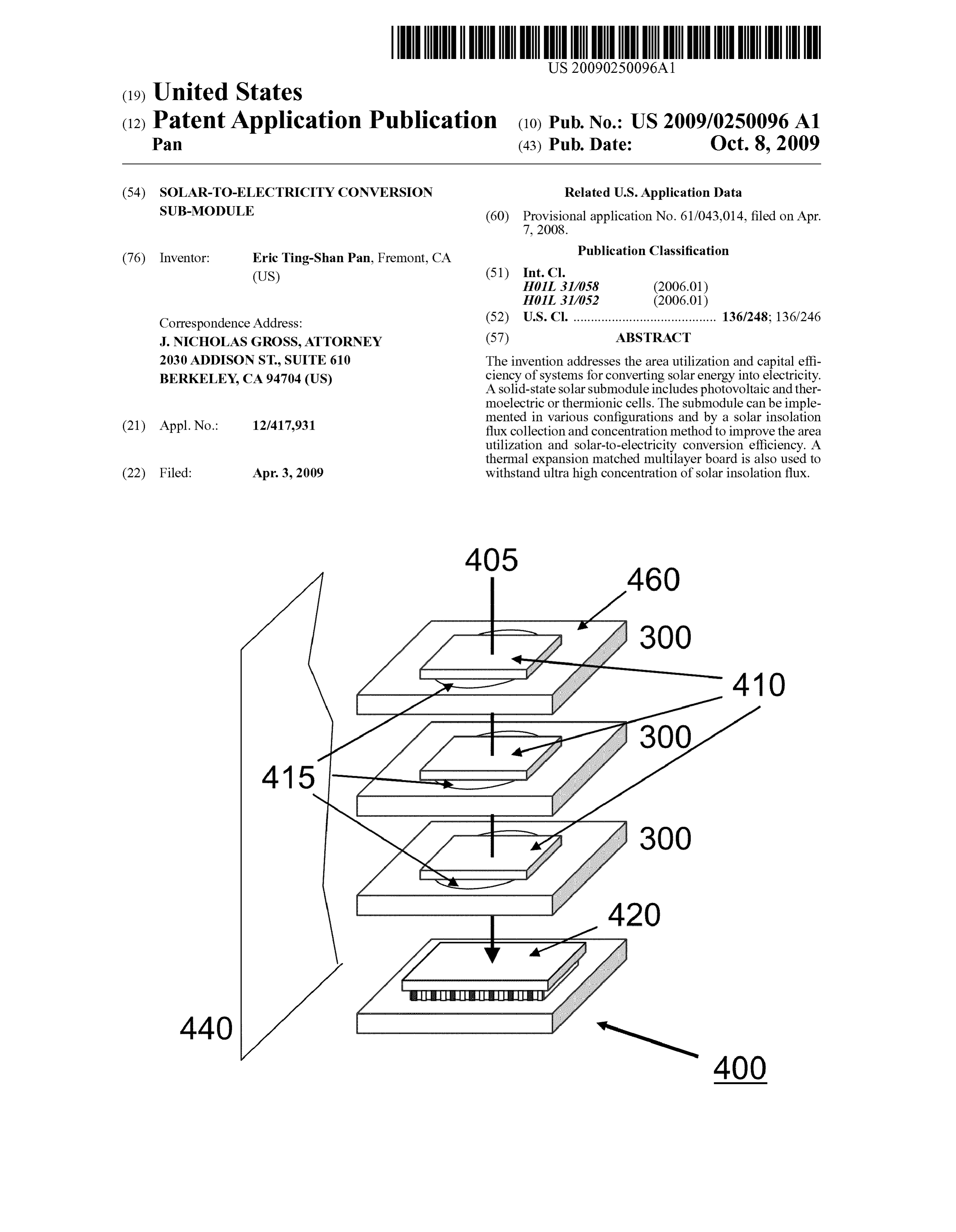
St. / 410
Page 2
Drawing sheet — no readable text.
Page 3
Drawing sheet — no readable text.
Page 4
Drawing sheet — no readable text.
Page 5
Drawing sheet — no readable text.
Page 6
Drawing sheet — no readable text.
Page 7
Drawing sheet — no readable text.
Page 8
Drawing sheet — no readable text.
Page 9
Drawing sheet — no readable text.
Page 10
Drawing sheet — no readable text.
Page 11
Drawing sheet — no readable text.
Page 12
Drawing sheet — no readable text.
Page 13
US 2009/025 0096 A1 Oct. 8, 2009
SOLAR-TO-ELECTRICITY CONVERSION 0013 Progress in Photovoltaics: Research and Applica SUB-MODULE tions, volume 11, issue 3 (Jan. 30, 2003), pp. 155-163. 0014. The most significant obstacle to wide deployment of
FIELD OF THE INVENTION solar electricity has been the figure of merit in cost per watt or kilo-watt-hour generated by a given Solar-to-electricity con 0001. The present invention relates to the field of solar version method. Current methods for manufacturing the Solar electricity and, more particularly, to the collection and con power generation require significant capital investment to version of Solar energy into electricity using Submodules that realize Volume production. Final products remain high in cost use concentrated Solar flux/insolation, and which can be which has prevented penetration into the large utility and assembled into larger Solar energy conversion systems. consumer markets as well as other niche markets. Contribut ing factors to cost include the conversion cell and its material,
BACKGROUND fabrication, package and assembly, frame and assembly, 0002 The collection of solar energy including photonic applicable Solar ray collection apparatus such as concentrator and thermal energies within the Solar spectrum and Subse and tracker, electrical system, transportation, and installation. 0015. A key parameter is the conversion efficiency—the quent conversion to electric power have been explored for ratio of electrical power output over Solar powerimpinging on many applications including, but not limited to, photovolta the Solar cell or module. Higher conversion efficiency means ics, concentrating photovoltaics, thermophotovoltaics, Solar higher power output per unit collection area and lower cost thermal power, concentrating Solar thermal power, active per output power. Another key parameter is the concentration Solar heating, and passive Solar heating, cooling, Solar factor—the ratio of the concentrated Solar radiation intensity thermo-electrochemical, and daylighting. In Solar collection, at the focal area to the flux at its collector aperture or, equiva there are a number of optical systems demonstrated for long lently, the ratio of the concentrated area at the focal point to term reliability such as flat-plates, flat-plates with side reflec the collector aperture area provided negligible loss of Solar tors, tubular collectors, paraboloids, parabolic troughs, flux along the path of concentration optics. Higher concen Fresnel lens or reflectors, heliostats with a central receiver, tration factor means Smaller footprint of the conversion and Stirling dishes with a refractance or a reflectance solar device and thus lower cost per output power. loss of typically 10%. These optical systems may or may not 0016. Accordingly there is clearly a long-felt need for be integrated with a one-axis or two-axes solar tracking sys Solar-to-electrical conversion systems (and components tem.
thereof) which are capable of addressing these deficiencies in 0003. The selection of an optical system depends on cost the prior art.
effectiveness, maintainability, cell materials, cell device and assembly, conversion efficiency, the degree of Solar concen SUMMARY OF THE INVENTION tration, and the methods to collect and/or track the sun. The concentration factor of these optical system collectors is pri 0017. An object of the present invention, therefore, is to marily limited by the temperature-dependent efficiency and overcome the aforementioned limitations of the prior art. It thermal stability of solar conversion method whether it is a will be understood from the Detailed Description that the working fluid in Solar thermal or a conversion device in Solar inventions can be implemented in a multitude of different photovoltaic. Among the top system performers at the time of embodiments. Furthermore, it will be readily appreciated by this invention, Stirling dish that uses a gas has operated with skilled artisans that such different embodiments will likely a conversion efficiency at about 40% and a concentration over include only one or more of the aforementioned objects of the 2,000x for solar thermal power and a lens-based concentrator present inventions. Thus, the absence of one or more of Such that uses a multi-junction Solar cell has performed at about characteristics in any particular embodiment should not be 40% conversion efficiency and 240x concentration factor. For construed as limiting the scope of the present inventions. multi-junction concentrator Solar cells, it is found that con 0018. A first aspect of the invention is directed to a solar version efficiency peaks out at about 600x before the thermal to-electricity conversion Submodule comprising: a photon expansion mismatch and associated thermal effects of mul to-electricity conversion device; a heat sink/pipe coupled to tiple stacking junctions or monolithically grown epitaxial the photon-to-electricity conversion device; a multi-layer layers become problematic. In particular, residual stresses board having a light cavity for receiving or transmitting radia induced by thermal expansion mismatch induce defects and tion flux associated with the photon-to-electricity conversion degrade conversion efficiency and occur in both lattice device; one or more conductive leads coupled to the photon matched and metamorphic (lattice-mismatched) epitaxial to-electricity conversion device for providing an electrical layered multi-junction Solar cell structures. output in response to radiation flux impinging on the photon 0004 Examples of solar to electrical conversion systems to-electricity conversion device; wherein the photon-to-elec can be seen in the following, all of which are hereby incor tricity conversion device, heat sink/pipe and conductive leads porated by reference herein: are located on and housed by or attached to the multi-layer board.
0006 U.S. Pat. No. 6,281,426 Olson, et al. 0019. The photon-to-electricity device is preferably based 0007 U.S. Pat. No. 7,109,408 Kucherov, et al. on a single junction cell adapted to convert only a first portion of an insolation flux spectrum into electrical energy based on 0008 U.S. Pat. No. 7,322,156 Rillie, et al. a first band gap energy. The module is further preferably 0009 U.S. Pat. No. 5,009,719 Yoshida adapted to be stacked into a cascade with one or more second 0010 U.S. Pat. No. 7,335,835 Kukulka, et al. modules having one or more photon-to-electricity devices 0011 U.S. Pat. No. 4,776,893 McLeod et al. based on single junction cells adapted to convert a second 0012 Ortiz, Estibalizet al., “A high-efficiency LPEGaAs different portion of the insolation flux spectrum into electrical solar cell at concentrations ranging from 2000 to 4000 suns.” energy based on one or more second band gap energies. The
Page 14
US 2009/025 0096 A1 Oct. 8, 2009
cascade is arranged in a linear arrangement such that the ity conversion device; wherein the multi-layer board is insolation flux travels in a straightline, or in an offset arrange adapted to have a thermal expansion characteristic that Sub ment such that the insolation flux is refracted and reflected stantially matches the photon-to-electricity conversion between different photon-electricity devices as it travels. device; one or more conductive leads coupled to the photon 0020. The multi-layer board is further preferably adapted to-electricity conversion device for providing an electrical to mounta thermionic orthermoelectric device in lieu of or in output in response to radiation flux impinging on the photon addition to the photon-to-electricity device, and is comprised to-electricity conversion device; wherein the photon-to-elec of a co-fired ceramic and conducting thermal vias, thermal tricity conversion device, heat sink/pipe and conductive leads diodes, bypass and/or blocking diodes, and embedded sen are located on and housed by the multi-layer board. sors and related electronic circuitry. In some embodiments 0027. Other aspects of the invention are directed to a larger the multi-layer board is further adapted to couple to a light Solar-to-electricity conversion system, in which the improve tube, a light guide or light pipe to receive the radiation flux. ment comprises a photovoltaic Subsystem including a plural 0021. In some embodiments the photon-to-electricity ity of photovoltaic cells having different band gaps to convert device includes reflector or a single or more reflection coat concentrated ultraviolet, visible, and infrared solar flux into ings are for reflecting a remaining radiation flux that is not electrical energy; and wherein the plurality of photovoltaic converted into electricity. cells are configured in a cascade arrangement for processing 0022. In other embodiments a plurality of photon-to-elec the concentrated ultraviolet, visible, and infrared solar flux. tricity devices having the same spectrum conversion capabil 0028 Preferably the cascade arrangement includes at least ity are arranged within the same plane and in a line to receive two photovoltaic cells arranged linearly such that the flux the radiation flux in a broad focal line. The focal line can be travels substantially in a straight line through the photovoltaic created by, among other things, a slit or light cavity mounted Subsystem, or they are arranged with an offset Such that the on the multi-layer board. flux is refracted and reflected between successive cells in the 0023. In some embodiments the photon-to-electricity con photovoltaic Subsystem.
version devices are situated and paired in a plane with other 0029. Each of the plurality of photovoltaic cells preferably matching photovoltaic cells, while other devices are situated is made from liquid phase epitaxy or gas diffusion, and and paired in a plane with respective matching photovoltaic includes an anti-reflection coating and/or a reflection coating cell, such that the concentrated insolation flux is converted by for spectrum selectivity of solar flux impinging on the device, a a two dimensional array into electrical energy. The devices one or more p-n junctions, one or more front conductor con can be paired with cells orthogonally positioned as well such tacts, and one or more back conductor contacts for electrical, that the concentrated insolation flux is converted by a three as well as contacts for heat conduction. The p-n junctions of dimensional array into electrical energy. the photovoltaic cells are preferably made of crystalline mate 0024. Another aspect of the invention concerns a solar-to rials.
electricity conversion Submodule comprising: a photon-to electricity conversion device adapted to convert insolation 0030 The cells can also include a single layer or multilay flux into electricity; a thermionic and/or thermoelectric ers of absorptive or anti-reflection costings for raising the device with a single or multiple anti-reflection and/or reflec absorption of a selective spectrum of the radiation flux that is tion coatings for spectrum selectivity situated along the path converted into electricity.
of solar flux to convertheat energy into electricity or adjacent 0031. In preferred embodiments a heat to electrical con to the photon-to-electricity device and adapted to convertheat version subsystem is situated in a path of the ultraviolet, energy associated with Such photon-to-electricity device into visible, and infrared solar flux and adapted to convertheat to electricity; a heat sink/pipe coupled to both the photon-to electricity. The invention can be paired with tracking sensors electricity conversion device and the thermionic and/or ther and motor drives that orient the conversion system toward the moelectric device; a multi-layer board having a light cavity Sun. Automated positioning mechanisms can be employed for for receiving or transmitting insolation flux: an electrical adjusting a spacing of the photon-to-electricity conversion combiner circuit coupled to both the photon-to-electricity devices.
conversion device and the thermionic and/or thermoelectric 0032. Further aspects of the invention concern a solar-to device and adapted to generate an electrical output in electricity conversion system comprising: a photovoltaic Sub response to the insolation flux: wherein the photon-to-elec system including at least two photovoltaic cells having dif tricity conversion device, thermionic and/or thermoelectric ferent band gaps to convert concentrated insolation flux into device, heat sink/pipe and electrical combiner circuit are electrical energy; at least two circuit boards for mounting and located on and housed by the multi-layer board. housing the at least two photovoltaic cells; wherein respective 0025. In preferred embodiments a position of the thermi junctions of the at least two photovoltaic cells are on separate onic and/or thermoelectric device can be automatically substrates or thin films situated on a respective circuit board; adjusted. Also, the multi-layer board preferably has a thermal a frame adapted for Supporting the at least two circuit boards expansion characteristic matching the photon to electricity and maintaining a first separation there between; wherein an conversion device. electrical output can be generated based on the concentrated 0026. A further aspect of the invention is directed to a insolation flux.
Solar-to-electricity conversion Submodule comprising: at 0033. In preferred embodiments of this type of system a least one photon-to-electricity conversion device having a light cavity can be coupled to one or more of the at least two single junction cell for converting only a first portion of an circuit boards, the least two circuit boards are thermally incident radiation spectrum into electricity; a heat sink/pipe matched to the respective at least two photovoltaic cells, have coupled to the photon-to-electricity conversion device; a embedded thermal conduction components, and diodes and/ multi-layer board having a light cavity for receiving or trans or other electrical circuitry to optimize Voltage and current mitting radiation flux associated with the photon-to-electric maximums of electricity generated by the system.
Page 15
US 2009/025 0096 A1 Oct. 8, 2009
0034) Furthermore at least one of the least two photovol flux; the photovoltaic cells including optical coatings, p-n taic cells can have a reflector for transmitting a remaining junctions, and conductor contacts for electrical and heat con unconverted spectrum of the concentrated insolation flux to a duction; wherein the p-n junctions of the photovoltaic cells Subsequent separate photovoltaic cell. The concentrated inso are made of crystalline materials; and the photovoltaic cells lation flux can received as a focal beam of a defined shape. being mounted on a multilayer board of cofired ceramic. 0035 Another aspect of the invention addresses a solar 0041 Another aspect of the invention is directed to a solar to-electricity conversion system comprising: a first photon to-electricity conversion system configured in a modular plat to-electricity conversion device adapted to convert a first form and comprising: a photon-to-electricity Subsystem spectrum portion of a concentrated insolation flux to electric including an array of Successive spaced photovoltaic cells ity; the first photon-to-electricity conversion device being having different band gaps to convert concentrated insolation situated in a first position within a path of the concentrated flux within a flux path into electrical energy; a heat-to-elec insolation flux: a second photon-to-electricity conversion tricity conversion subsystem also situated within the flux path device situated adapted to convert a second spectrum portion and including at least one of an array of thermoelectric cells or of a remainder of the concentrated insolation flux to electric thermionic cells to covert heat into electric energy; a heat ity; the second photon-to-electricity conversion device being sink/pipe coupled to the photon-to-electricity Subsystem and/ situated in a second position separated from the first position or the heat-to-electricity conversion Subsystem; a plurality of within the path of the concentrated insolation flux: a heat to thermal expansion matched multilayer boards for integrating electrical conversion Subsystem situated in a third position the photon-to-electricity subsystem, the heat-to-electricity within the path of the concentrated insolation flux and includ conversion Subsystems and heat sink/pipe; a light cavity situ ing at least one of an array of thermoelectric cells and/or ated within the flux path and adapted to direct the concen thermionic cells to covertheat associated with a third spec trated insolation flux between the Successive spaced photo trum portion of the concentrated insolation flux into electric Voltaic cells; and an assembly for mounting the photon-to energy; a frame adapted for Supporting the first and second electricity Subsystem, the heat-to-electricity conversion photon-to-electricity conversion devices and the heat to elec Subsystem, the heat sink/pipe, the plurality of thermal expan trical conversion Subsystem; wherein electrical power can be sion matched multilayer boards and the light cavity. derived from at least the first spectrum portion, the second 0042. A further aspect concerns a solar-to-electricity con spectrum portion and the third spectrum portion of the con version system configured in a modular platform and com centrated insolation flux. prising: a photon-to-electricity Subsystem including a linear 0036) The heat to electrical conversion subsystem can be cascade arrangement of two or more Successive spaced pho situated in a variety of locations, including before the first tovoltaic cells, each of the cells having a different bandgap to photon-to-electricity conversion device and/or after a lastone convert concentrated insolation flux within a flux path into of the photon-to-electricity conversion devices within the electrical energy; a heat-to-electricity conversion Subsystem concentrated insolation flux path. As alluded to above the first also situated immediately before or after the photon-to-elec photon-to-electricity conversion device, the second photon tricity Subsystem within the linear cascade arrangement and to-electricity conversion device, and the heat to electrical flux path and including at least one of an array of thermoelec conversion Subsystem can be configured or in an offset tric cells or thermionic cells to convert heat into electric arrangement such that the concentrated insolation flux is energy; a heat sink/pipe coupled to the photon-to-electricity refracted and reflected between one or more successive cells Subsystem and/or the heat-to-electricity conversion Sub and/or the heat to electrical conversion Subsystem. system; a plurality of thermal expansion matched multilayer 0037. The thermoelectric cells in the heat to electrical boards, one for each of the photovoltaic cells and the array of conversion Subsystem preferably include: a cascade of crys thermoelectric or thermionic cells; and a casing assembly for talline thermoelectric cells of one or multiple types of junc mounting the photon-to-electricity Subsystem, the heat-to tion materials absorbing infrared radiation or heat; and the electricity conversion Subsystem, the heat sink/pipe, the plu thermoelectric cells further including a single or multiple rality of thermal expansion matched multilayer boards and anti-reflection and/or reflection coatings for spectrum selec the light cavity.
tivity, p-n junctions, front conductor contacts, and back con 0043. In preferred embodiments the two or more succes ductor contacts for electrical and, separate heat conduction; sive spaced photovoltaic cells include the following: a first and the p-n junctions of the thermoelectric cells are made of photovoltaic cell of band gap at about 2.54 eV; a second crystalline materials. photovoltaic cell of band gap at about 1.47 eV; and a third 0038. The thermionic cells in the heat to electrical conver photovoltaic cell of bandgap of about 0.7 eV. Furthermore the sion Subsystem preferably include: a single or multiple anti first photovoltaic cell is AlGaAs; the second photovoltaic cell reflection and/or reflection coatings on the hot side for spec is GaAs; and the third photovoltaic cell is GaSb or Ge. trum selectivity; an array of alternating n-type and p-type 0044. Yet another aspect concerns a solar-to-electricity thermal diodes; wherein the thermal diodes are shaped into conversion system configured in a modular platform and columns using a via structure embedded in a multilayer comprising: a photon-to-electricity Subsystem including an board; a hot side conductor contact; a cold side conductor offset cascade arrangement of two or more Successive spaced contact; and electrical interconnect to couple the thermal photovoltaic cells, each of the cells having a different band diodes and electrical contacts. gap to convert concentrated insolation flux within a flux path 0.039 Embodiments of the invention can be used to form a into electrical energy; wherein the concentrated insolation Solar energy power generating plant. flux is reflected between successive photovoltaic cells as it 0040. Other aspects of the invention concern a photon-to traverses the offset cascade arrangement; a heat-to-electricity electricity Subsystem comprising: a cascade of photovoltaic conversion subsystem situated immediately before the pho cells of different band gaps and each of one or more p-n ton-to-electricity Subsystem for reflecting the concentrated junctions absorbing ultraviolet, visible, and infrared Solar insolation flux into the offset cascade arrangement and
Page 16
US 2009/025 0096 A1 Oct. 8, 2009
including at least one of an array of thermoelectric cells or wherein the photovoltaic modules each include one or more thermionic cells to convert heat into electric energy; a heat photovoltaic cells situated in a planar arrangement within the sink/pipe coupled to the photon-to-electricity Subsystem and/ focal line; a heat-to-electricity conversion Subsystem situated or the heat-to-electricity conversion Subsystem; a plurality of immediately before or after the photon-to-electricity sub thermal expansion matched multilayerboards, one for each of system within the focal line and including at least one of an the photovoltaic cells and the array of thermoelectric or ther array of thermoelectric cells or thermionic cells to convert mionic cells; a casing assembly for mounting the photon-to heat from the concentrated insolation flux into electric electricity Subsystem, the heat-to-electricity conversion Sub energy; a heat sink/pipe coupled to the photon-to-electricity system, the heat sink/pipe, and the plurality of thermal Subsystem and/or the heat-to-electricity conversion Sub expansion matched multilayer boards. system; a plurality of thermal expansion matched multilayer 0045 Another aspect of the invention is directed to a solar boards, one for each of the photovoltaic cells and the array of to-electricity conversion system configured in a modular plat thermoelectric or thermionic cells; a casing assembly for form and comprising: a first light directing means for receiv mounting the photon-to-electricity Subsystem, the heat-to ing concentrated insolation flux: a photon-to-electricity electricity conversion Subsystem, the heat sink/pipe, the plu Subsystem including an offset cascade arrangement of two or rality of thermal expansion matched multilayer boards and more Successive spaced photovoltaic cells, each of the cells the light cavity.
having a different band gap to convert the concentrated inso lation flux within a flux path into electrical energy; second 0048 Still another aspect concerns a solar-to-electricity light directing means positioned between the two or more conversion system configured in a modular platform and pro Successive spaced photovoltaic cells; wherein the concen cessing concentrated Solar insolation flux incidence into the trated insolation flux is reflected between the successive pho Solar-to-electricity conversion system with a concentration tovoltaic cells within the second light directing means as it factor between 250x and 5,000x comprising: a photovoltaic traverses the offset cascade arrangement; a heat-to-electricity subsystem including an array of photovoltaic cells of differ conversion subsystem situated immediately before the pho ent band gaps and each cell having an area between about 300 ton-to-electricity Subsystem for reflecting the concentrated hundred square microns to 30 square centimeters to convert insolation flux into the linear cascade arrangement and concentrated solar visible, ultraviolet, and infrared radiation including at least one of an array of thermoelectric cells or into electrical energy; a thermoelectric or a thermionic Sub thermionic cells to convert heat into electric energy; a heat system including a plurality of thermoelectric or thermionic sink/pipe coupled to the photon-to-electricity subsystem and/ cells to convert at least the concentrated solar infrared radia or the heat-to-electricity conversion Subsystem; a plurality of tion and/or a temperature gradient into electrical energy; a thermal expansion matched multilayerboards, one for each of frame adapted to Support and function as an environmental the photovoltaic cells and the array of thermoelectric or ther shield and which is integrated as part of the hot side and/or mionic cells; and a casing assembly for mounting the photon cold side (heat sink) in the heat-to-electricity conversion; a to-electricity Subsystem, the heat-to-electricity conversion first light directing means for directing the concentrated Solar Subsystem, the heat sink/pipe, the plurality of thermal expan insolation flux incidence and any reflectance unto the photo sion matched multilayer boards and at least the second light Voltaic and thermoelectric or thermionic Subsystems; a ther directing means. mal expansion matched multilayer board adapted to integrate 0046 Still another aspect concerns a solar-to-electricity components (a) and (b) and to transfer heat among Such conversion system configured in a modular platform and components by thermal vias; and a second light directing comprising: a photon-to-electricity Subsystem including a means in the multilayer board adapted to direct concentrated linear cascade arrangement of two or more successive spaced solar insolation flux between photovoltaic cells. photovoltaic cells, each of the cells having a different band 0049 Other aspects of the invention concern methods of gap to convert concentrated insolation flux within a flux path converting concentrated ultraviolet, visible, and infrared into electrical energy; a heat-to-electricity conversion Sub Solar flux to electrical energy using the above architectures system situated immediately before the photon-to-electricity and configurations. In addition the Solar insolation flux can be Subsystem for reflecting the concentrated insolation flux into collected by one or more of: a dome of a Fresnel lens system, the linear cascade arrangement and including at least one of a parabolic trough parabolic trough, a linear Fresnel lens, a an array of thermoelectric cells or thermionic cells to convert hemispherical bowl collector, a flat absorbing plate, a cylin heat into electric energy; a heat sink/pipe coupled to the drical collector, oran active steering or a motion-free tracking photon-to-electricity subsystem and/or the heat-to-electricity collector with concentration or spectrum splitting function. conversion Subsystem; a plurality of thermal expansion From there it is presented to a cascade of photon-to-electricity matched multilayer boards, one for each of the photovoltaic devices and/or heat-to-electricity devices. The electrical cells and the array of thermoelectric or thermionic cells; and energy generated can be used to charge an electric Storage a casing assembly for mounting the photon-to-electricity Sub apparatus, or be delivered to a balance-of-system for deliver system, the heat-to-electricity conversion Subsystem, the heat ing electricity.
sink/pipe, and the plurality of thermal expansion matched 0050. Other aspects of the invention concern a production multilayer boards. method for making crystalline photovoltaic cells and/or ther 0047 A further aspect of the invention is directed to a moelectric or thermionic cells the improvement comprising Solar-to-electricity conversion system configured in a modu forming the crystalline photovoltaic and/or thermoelectric or lar platform and comprising: a photon-to-electricity Sub thermionic cells and interfaces by liquid-phase epitaxial system including a first linear cascade arrangement of two or growth, gas diffusion, or some other equivalent process. The more Successive spaced photovoltaic modules, each of the process further preferably includes a step of growing a seed modules having a different band gap to convert concentrated layer and/or a sacrificial layer using metalorganic chemical insolation flux within a focal line into electrical energy; vapour deposition (MOCVD) or an epitaxy growth method.
Page 17
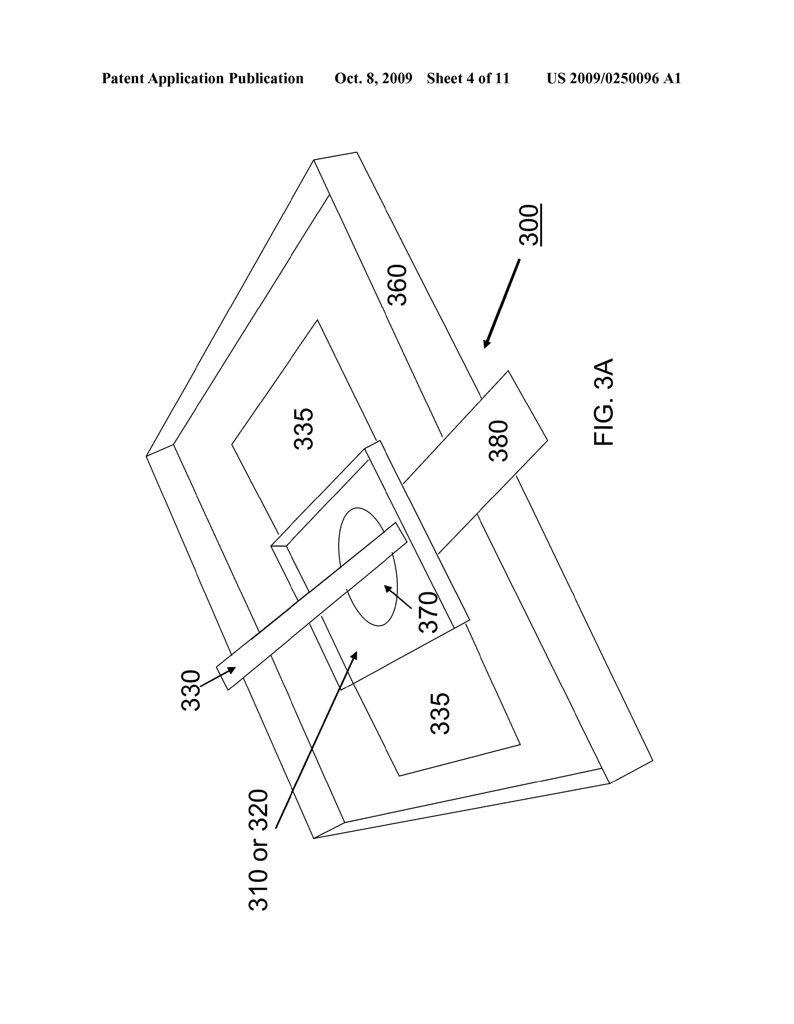
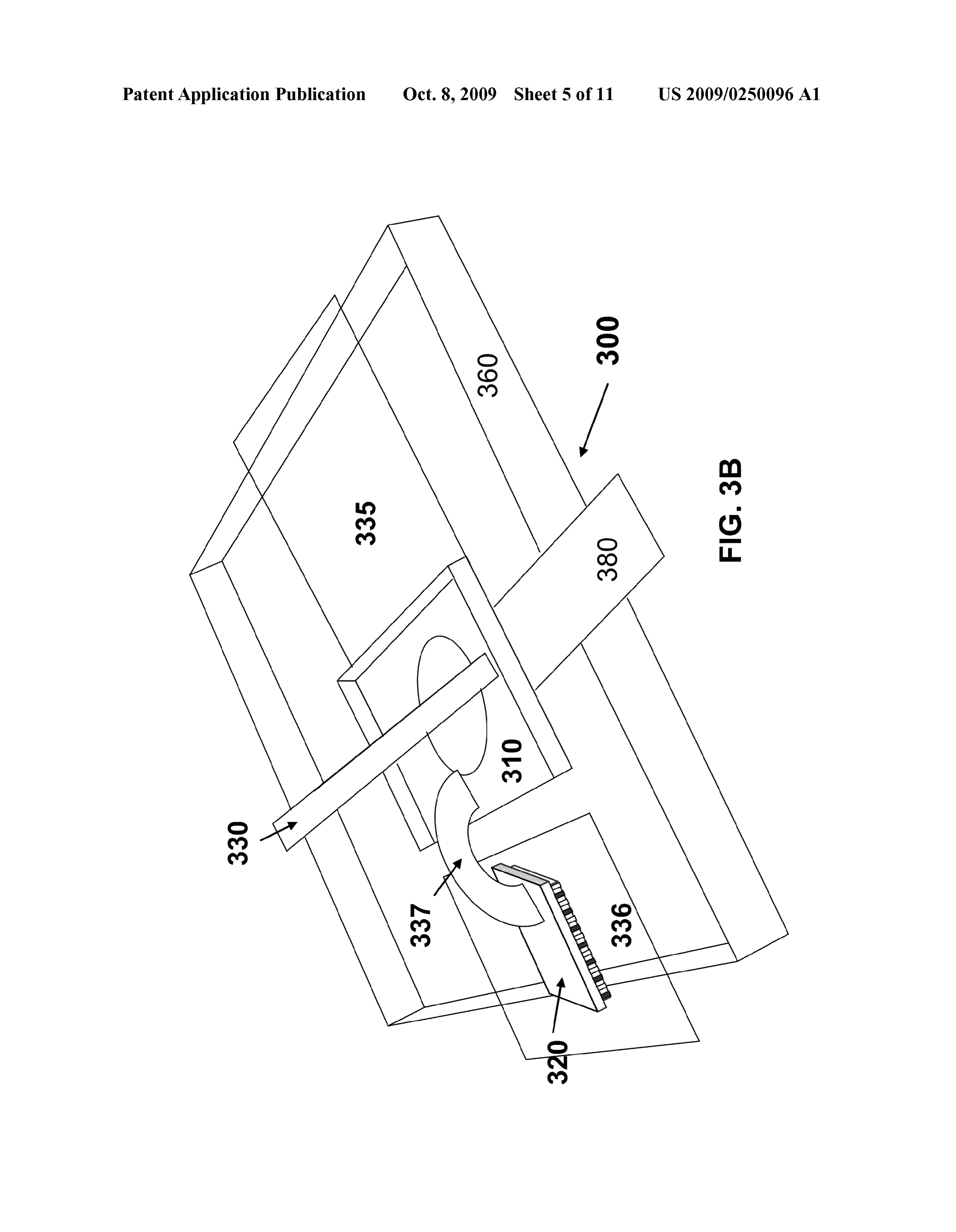
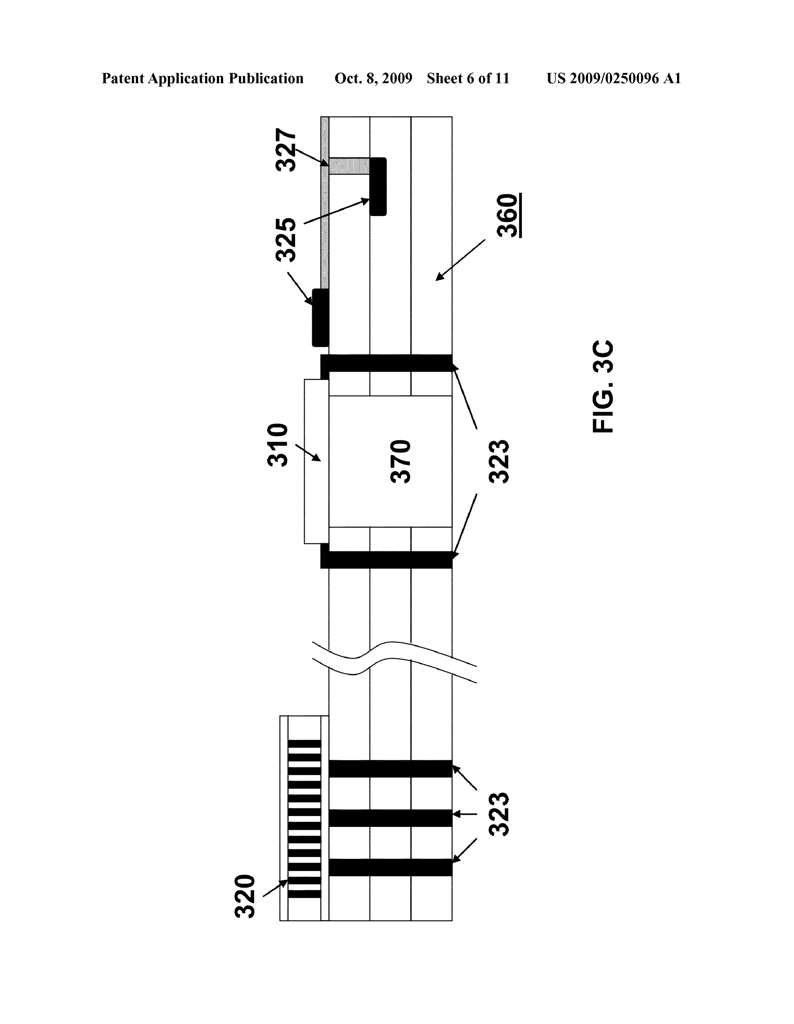
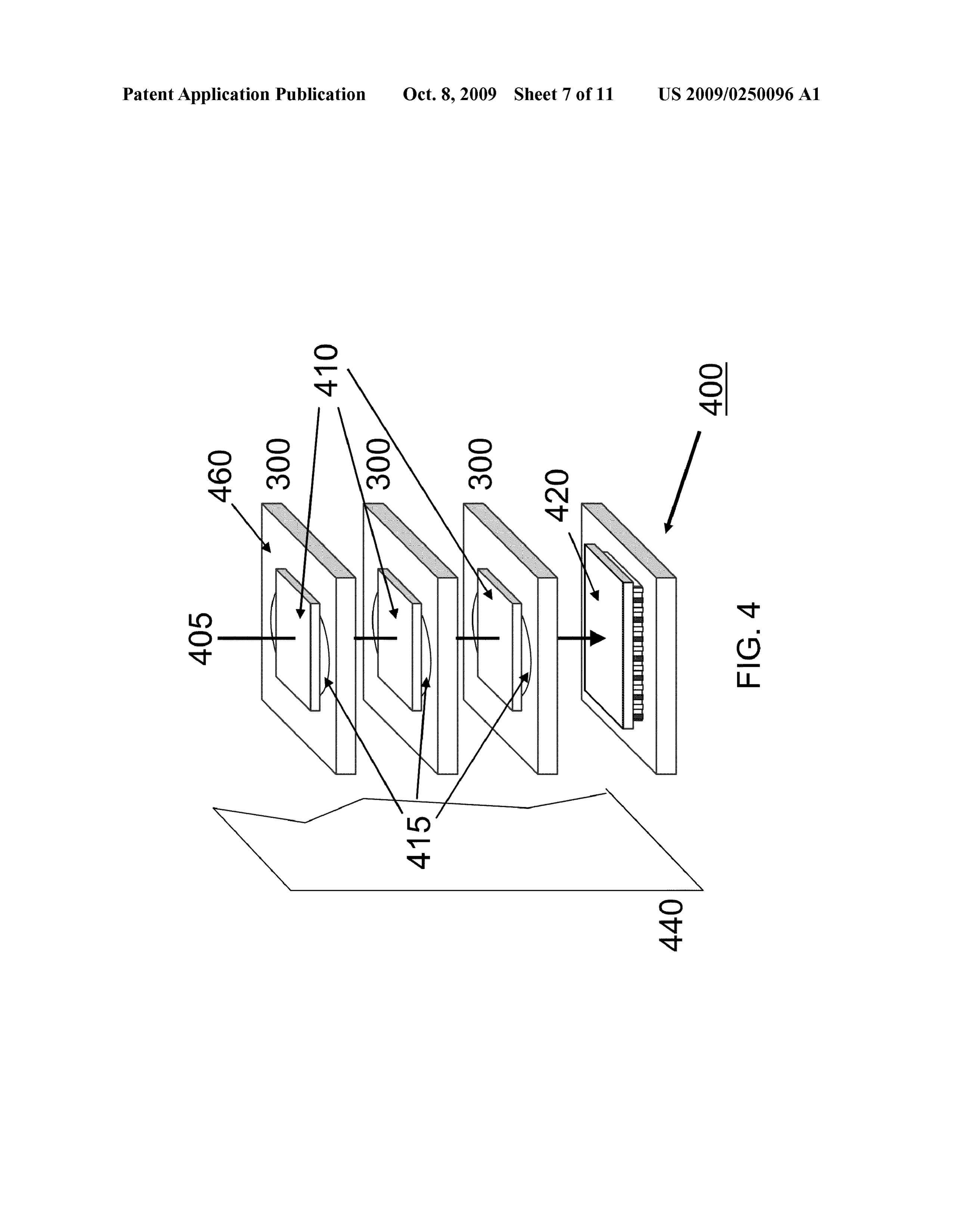
US 2009/025 0096 A1 Oct. 8, 2009
0051 While described in the context of a solar conversion multi-junction solar cell occurs between different constituent system, it will be apparent to those skilled in the art that the layers under elevated temperature that leads to thermal present teachings could be used in any number of other sys residual stresses, which affect the integrity and lifetime of the tems in which it is desirable to improve efficiency of a radia photovoltaic cells, under high concentrated Solar flux. It is tion conversion process. Embodiments of the invention are known for a single-crystal cell under no external influence, its expected to be used for both terrestrial and extra-terrestrial coefficient of thermal expansion (CTE) is complaint with the applications where it is desired to make use of Solar power— crystal symmetry.
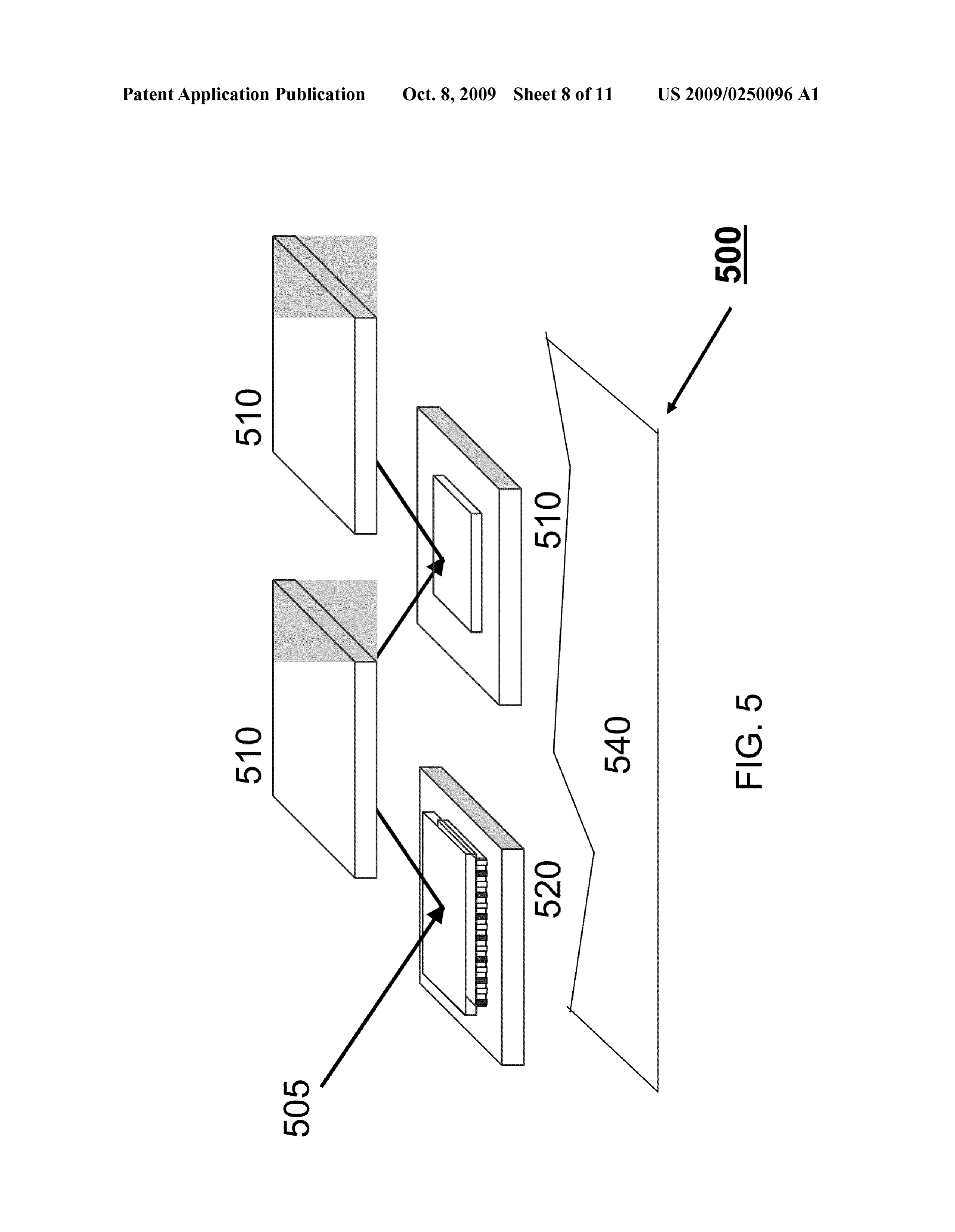
Such as part of a satellite, a space transport, robotic explora 0066. A single-crystal photovoltaic cell as used in pre tion vehicle, a housing unit, a building, a Solar power plant, space station, a Solar powerplant, off-grid and grid-connected ferred embodiments of the present invention can, therefore, facilities, etc. handle higher concentrated Solar flux and temperature than the prior-art multi-junction photovoltaic cells. The modular
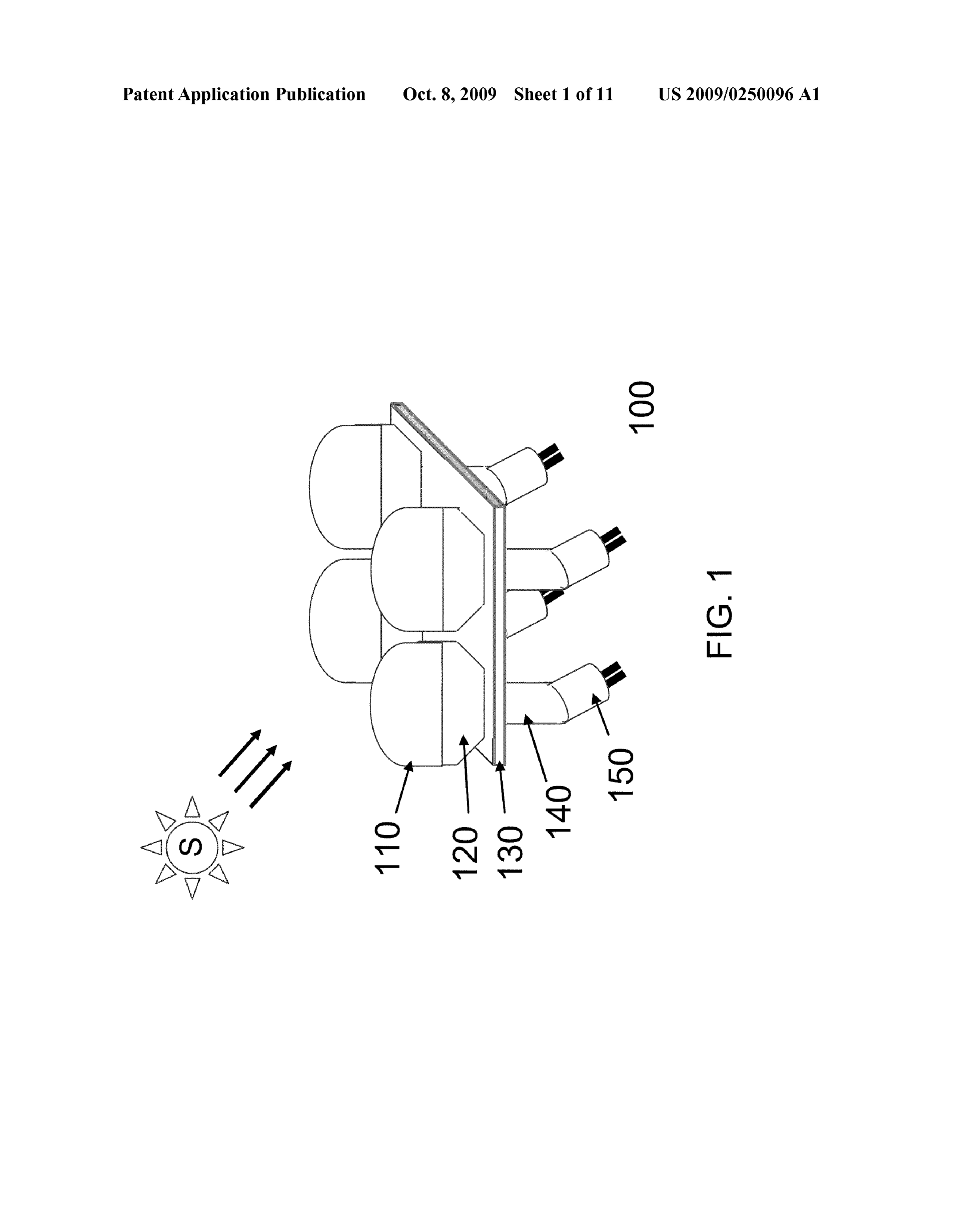
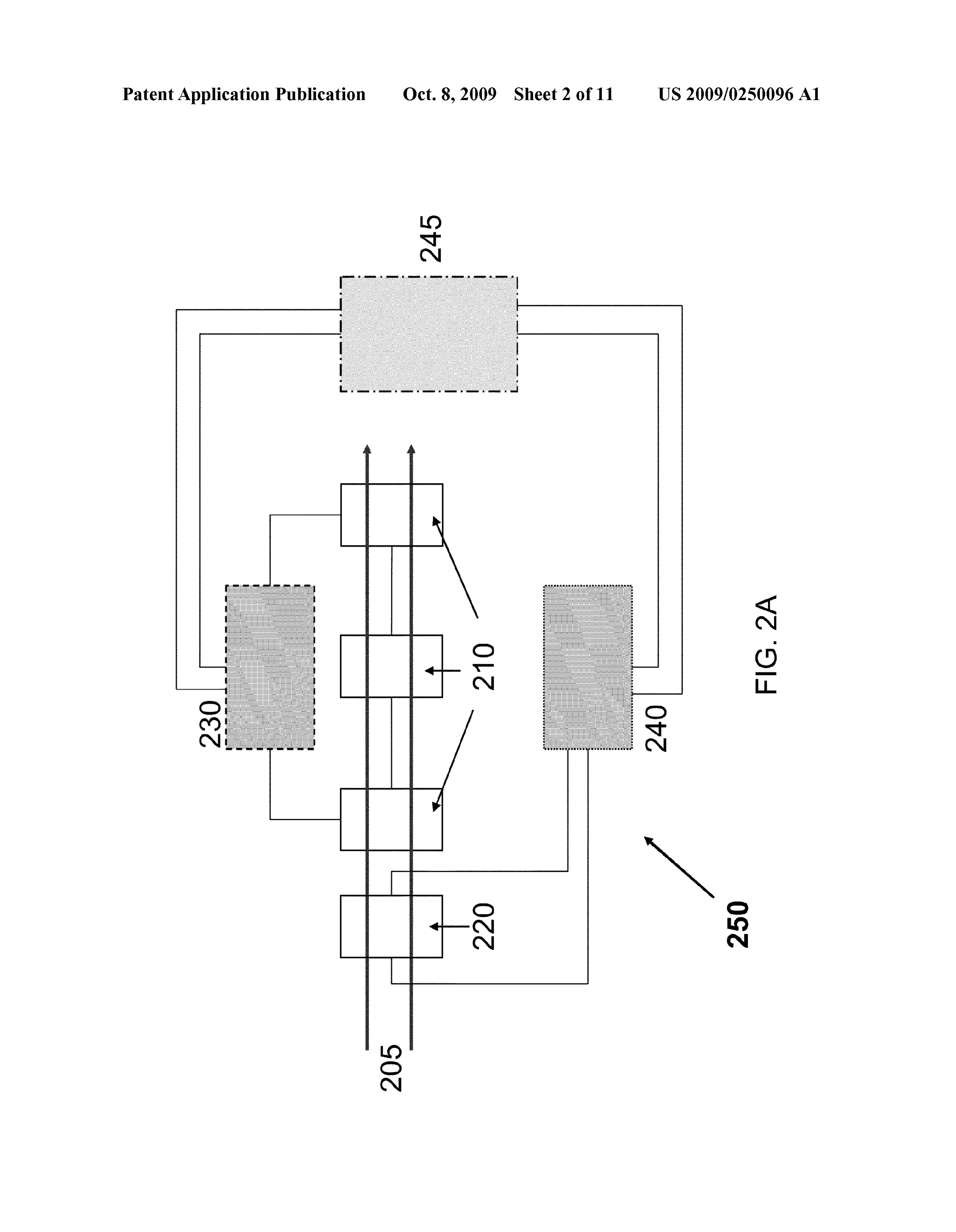
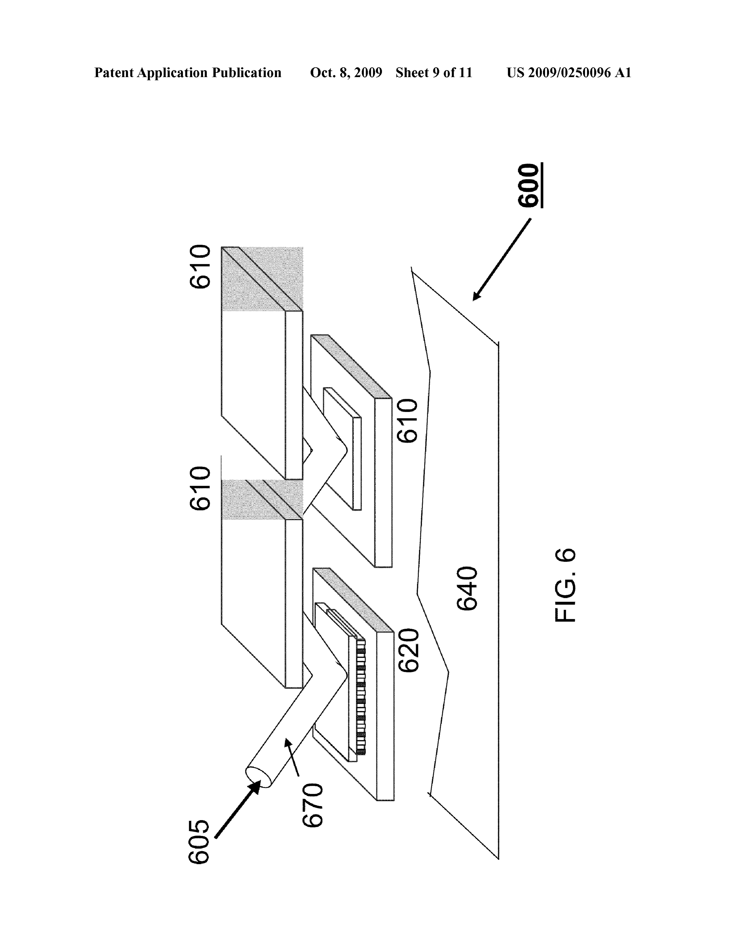
DESCRIPTION OF THE DRAWINGS platform described herein arranges the single-crystal photo voltaic cells to absorb solar flux in a cascade such that the first 0052 FIG. 1 is a simplified diagrammatic view of a pre cell absorbs a portion of the solar flux with energy above its ferred embodiment of a solid-state solar engine system of the band gap and the second cell absorbs, with energy above the present invention; second cell's band gap, a portion of the Solar flux that is not 0053 FIG. 2A is an illustrative configuration of a pre absorbed by the first cell, and so on. For semiconductor-based ferred embodiment of a solar-to-electricity converter module: photovoltaic materials, the band gap generally refers to the 0054 FIG. 2B is an illustrative configuration of an alter energy difference between the top of the valence band and the nate embodiment of a solar-to-electricity converter module in bottom of the conduction band.
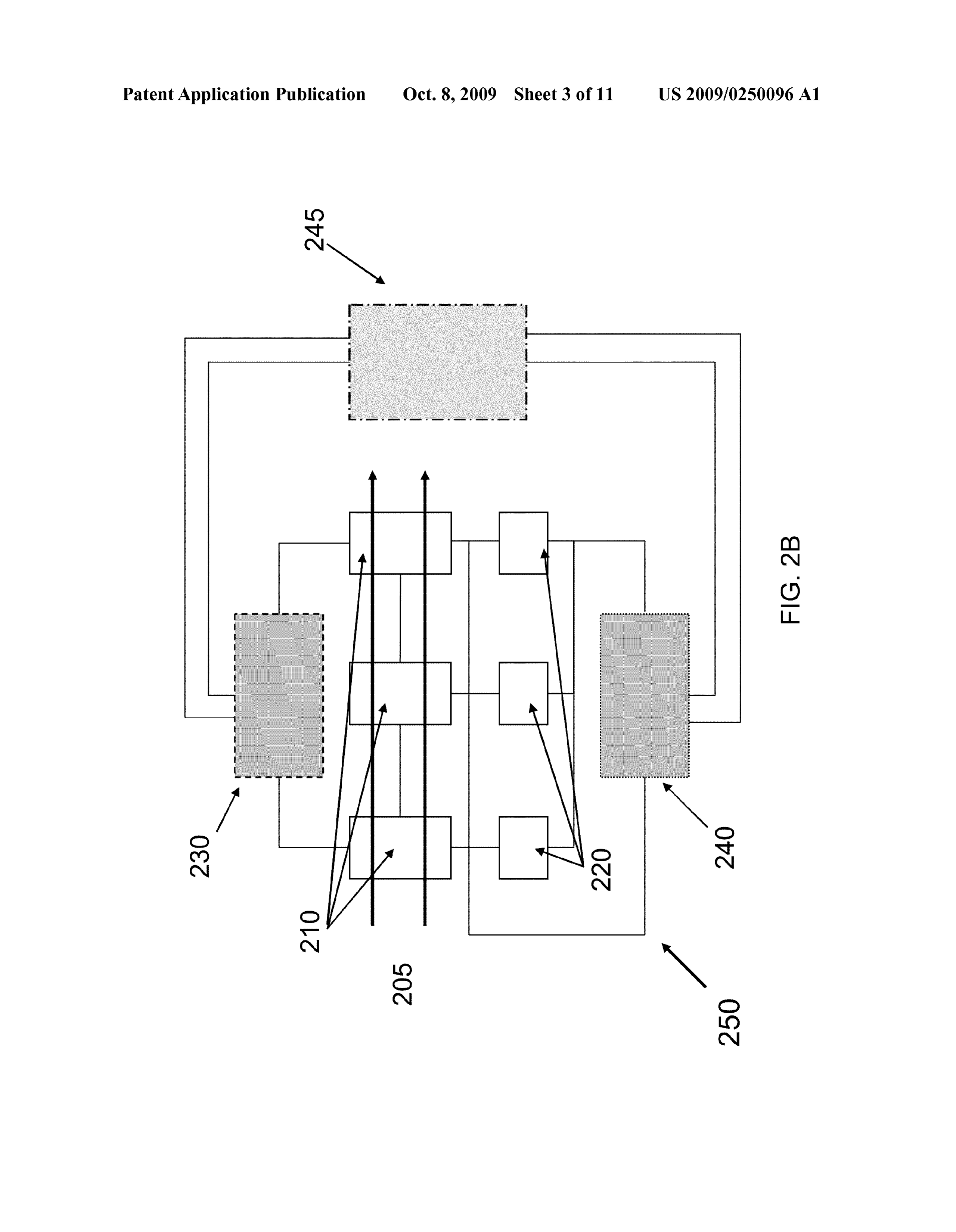
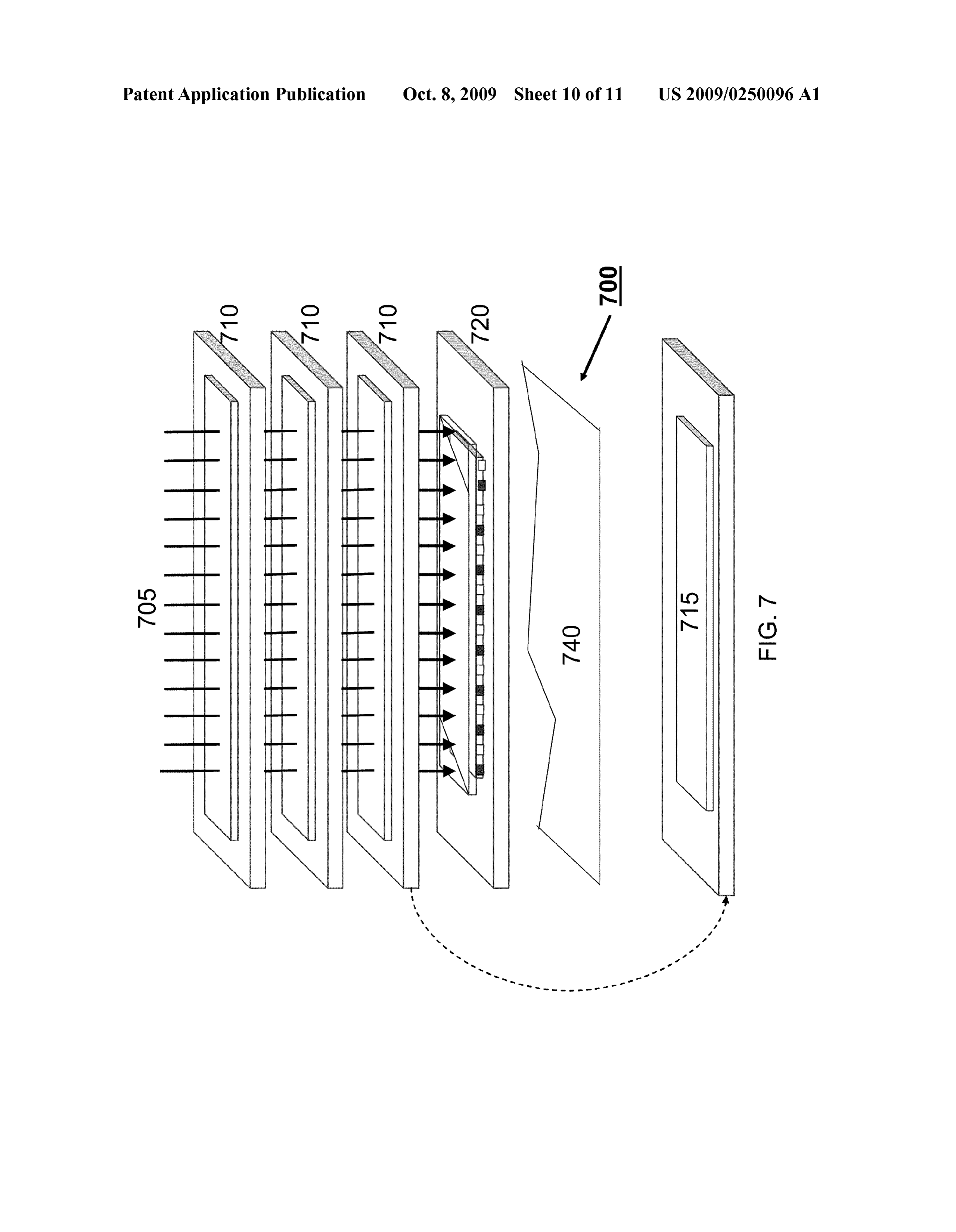
which athermoelectric/thermionic device is coupled to one or 0067 Furthermore, preferred embodiments exploit the more photoelectric device: conversion of thermal energy to electric energy using ther 0055 FIG. 3A is a diagrammatic view of common com moelectric and thermionic converters. In particular, a prior art ponents of a preferred embodiment of a packaged cell; Solid-state thermionic converter using semiconductor diode 0056 FIG. 3B is an illustrative configuration of an alter has sufficient high power densities and efficiencies and can nate embodiment of a cell in which a thermoelectric/thermi onic device is coupled to a photoelectric device; operate attemperature range for a broad scope of application potentials. In some embodiments the Solar energy converter 0057 FIG. 3C is a cross sectional view of a packaged comprising the aforementioned cascading single crystal pho sub-module: tovoltaic cells and the solid-state thermionic devices utilizes 0058 FIG. 4 is a diagrammatic view of a converter module and transfers heat from the interaction between solar flux and according to one embodiment of the present invention; a solid-state matter to a solid-state thermionic device for 0059 FIG. 5 is a diagrammatic view of a second embodi heat-to-electricity conversion.
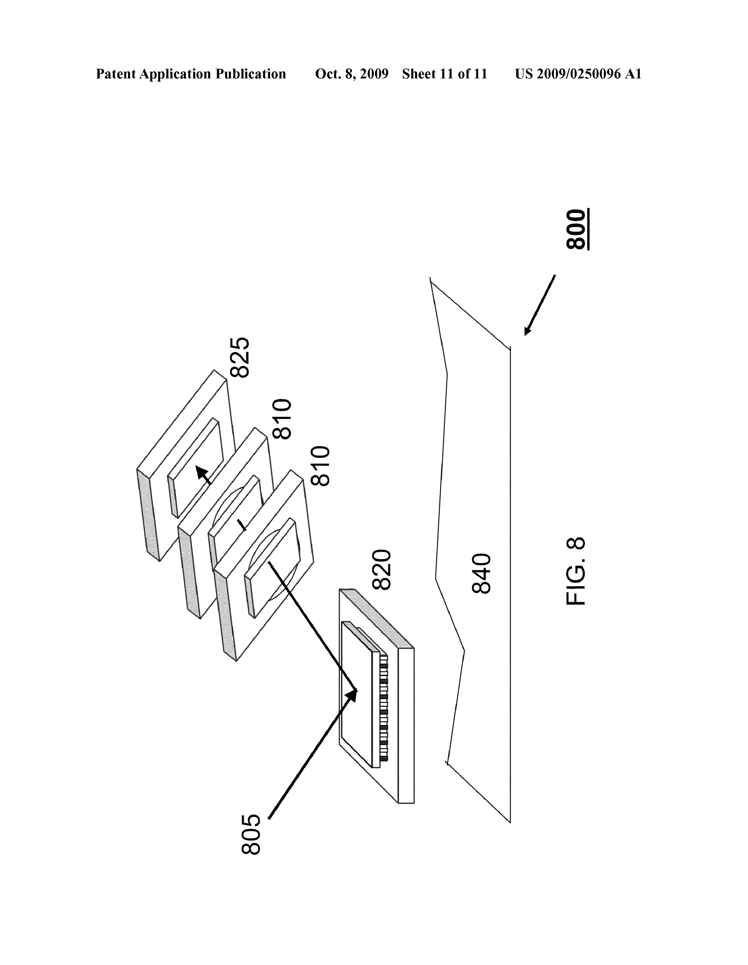
ment of a converter module: 0068 Another advantage of certain preferred embodi 0060 FIG. 6 is a diagrammatic view of a third embodi ments is that a single crystal cell of high quality can be ment of a converter module: fabricated with a method that forms a layer interface of true 0061 FIG. 7 is a diagrammatic view of a fourth embodi thermodynamic equilibrium Such as by using a prior-art liq ment of a converter module: uid-phase epitaxy method that is not currently used for the 0062 FIG. 8 is a diagrammatic view of a fifth embodiment mass production of Solar cells. The liquid phase epitaxy of a converter module: method may be improved for mass production with active
DETAILED DESCRIPTION
epitaxy growth control and high throughput layer formation mechanism. Among other aspects the present invention pro 0063 A novel modular platform integrates solid-state poses a new application by using an improved liquid phase photovoltaic and thermionic or thermoelectric devices with epitaxy method for the mass production of high quality single the Solar collection and concentration optics for the Solar-to crystal Solar cells with low dislocations and defects and uni electricity conversion. Both the conversion efficiency and the form layers and interface. High crystal quality yields signifi heat handling capability under a focal area of high Solar cant advantage with high conversion efficiency because of concentration are increased by cascading photon-to-electric low defect density and exceptional optical quality because of ity devices such as photovoltaic devices and heat-to-electric high degree of homogeneity and interfacial uniformity. ity devices such as Solid-state thermionic and thermoelectric 0069 Finally, another useful aspect of embodiments of the devices, each of which is made of specific composition. invention is that the the solar energy converter can be fabri 0064. Embodiments of the present invention thus provide cated with a method that is fully compatible with conven a conversion system that is scalable for the photovoltaic tional low-temperature cofired ceramic process technology device of area from a few hundreds of micron square to a few for assembling the cells into packages. The coefficient of tens of centimeter square with the corresponding optical col thermal expansion of low-temperature cofired ceramic can be lection area that gives a concentration factor from 250x to matched to that of the solar-to-electricity conversion die 5,000x. The overall conversion efficiency of the solid-state attached to it for thermal stability under high solar concen Solar engine module of the present invention has potential to tration. A customized light cavity can be incorporated into the achieve 50% or more of which the conversion from photon to low-temperature cofired ceramic process for special module electricity is greater than 40% and the conversion from heat to configurations.
electricity is greater than 10%. (0070 Referring initially to FIG. 1 a preferred embodiment 0065. The present disclosure describes an alternative solu of a solar-to-electricity conversion system 100 according to tion to the prior-art multi-junction Solar cell or photovoltaic the present invention is shown. It will be understood by those cell. The problem of thermal expansion mismatch in the skilled in the art that the depiction provided is not intended to
Page 18
US 2009/025 0096 A1 Oct. 8, 2009
show exact dimensions, shapes, and/or proportions as may be improve conversion efficiency, concentration factor, and ther used in a commercial application. mal handling capability. Again for illustrative purposes the 0071. The system 100 generally includes a collector 110, a present diagram and discussion is simplified and skilled arti concentrator 120, a frame 130, a light tube/guide/fiber/pipe sans will appreciate that other components could be 140, and a converter module 150 which is the subject of employed in deployed application.
substantial discussion below. It will be apparent to those (0079 Radiation 205 (preferably solar flux) falls on the skilled in the art that the present discussion is simplified in converter module as a source of photons to be converted to order to elaborate the main aspects of the invention, and that electricity. Preferably the converter module 250 comprises a other elements could be employed as well in other embodi cascade arrangement of one or more photon-to-electricity ments depending on system requirements. devices 210, one more heat-to-electricity devices 220, a first 0072 Collector 110 is preferably one of a conventional power control circuit 230 for photon-to-electricity charge dome of a Fresnel lens system with high optical conversion to control, a second power control circuit 240 for heat-to-elec collect low and high angle Solar rays (or other radiation tricity charge control, and a circuit combiner 245 as part of the Source). Alternatively a combined optical system can be used balance-of-system that may be placed external to a unit mod for the dual purposes of a collector and a concentrator Such as ule.
an active steering collector or a motion-free tracking collector 0080. The first power controller circuit 230 can be with concentration or spectrum splitting function. arranged such that the photocurrent and photovoltage from 0073 Concentrator 120 is preferably one of the following: each photon-to-electricity device 210 can be combined a conventional parabolic trough/reflector, a set of two reflec within a Solar-to-electricity converter module or connected in tors, a linear Fresnel lens, a hemispherical bowl collector, a parallel or series with devices of other modules (shown in cylindrical collector, a focusing lens, a tapered light tube, a FIG. 1) to form the next levels of integration as in a panel and light guide, a light fiber, or a light pipe for directing all the an array (not shown) for desired electrical characteristics. The photons collected after the collector 110 to a focal area such Solar radiation 205, consisting of a first spectrum of energetic as a focal spot or a focal line that is reduced from the collector photons, impinges on the cascade of photovoltaic devices 210 aperture area by approximately the concentration ratio. and a thermoelectric or thermionic device 220. 0074 Frame 130 is preferably comprised of planks, I0081. The thermoelectric or thermionic device 220 is pref frames, conduits, enclosures, racks or other Suitable struc erably placed within the cascading order So that Solar radia tures and is mounted on a roof-top, a stand, a tracking mount, tion incidence can be extracted from a position before the first a cladding, or any supporting structure for optimal solar col photovoltaic device 210, after the last such device, or in both lection and structure support of the entire system 100. The locations. Coatings such as that absorb infrared and/or ultra frame 130 may be configured to serve to shield the light violet and reflect visible may be applied on the surface of the tube/guide/fiber/pipe 140 and the converter module 150 from thermoelectric or thermionic device upon which solar radia environmental factors such as air temperature, air humidity, tion incidence hits. The thermoelectric or thermionic device water, wind, etc. The frame 130 may also be configured as a thus captures and converts thermal energy from that portion part of heat sinks/pipes for the photovoltaic conversion. The of the spectrum which would otherwise not be sufficient to frame 130 may further serve in a preferred modular configu activate electrons from the valence band to the conduction ration to be integrated into the thermionic and thermoelectric band across a band gap in a photovoltaic device. It will be conversion as part of a hot side or a cold side. In some understood of course that the heatenergy converteris optional embodiments frame 130 may even further consist of separate and will not be necessary or required in many installations. layers or regions as a hot side and a cold side for the thermi 0082 An alternative embodiment for the conversion mod onic and thermoelectric conversion. ule 250 is shown in FIG. 2B. In this configuration the ther 0075 Light tube 140 is preferably a conventional appara moelectric/thermionic devices 220 are directly physically/ tus for guiding light rays from the concentrator 120 to the mechanically coupled to the photovoltaic devices 210, and converter module 150. extract heat that is associated with Such devices, rather than 0076. Other examples will be apparent to those skilled in deriving directly from within the solar flux beam. In some the art for components 110-140, and it is expected that the embodiments the positioning of the thermoelectric orthermi particular components and configuration will vary Substan onic device 220 can be adaptively varied (by an automated tially from application to application depending on perfor mechanical positioning system) in accordance with an opti mance requirements, cost constraints, etc. Moreover while mal behavior observed at a particular location/installation/ certain current conventional examples of Such components time of year. It will be understood by those skilled in the art have been described, it will be understood that the present that other embodiments may utilize features from both of invention can be used with other variants, advances, etc. of these approaches, and the invention is not so limited. Such components which are not yet well known and/or undis I0083. Although the solar spectrum and photonic device covered. physics are well known in the art and many prior-art photo 0077. In addition solar conversion system 100 can be inte Voltaic cells with various compositions and band gaps have grated into a conventional balance-of-system typically com been fabricated, the present invention provides further posed of charge control, storage, inverter, electrical cabling, improvement to the photon-to-electricity conversion effi and protection circuitry for off-grid and on-grid applications. ciency and the concentration factor through a modular plat Energy storage (not shown) may use prior-art direct electric form capable of integrating the photon-to-electricity and storage such as ultracapacitors or electrochemical energy heat-to-electricity conversion devices. Unlike a conventional storage Such as batteries. prior-art multi-junction solar cell that operates with limited 0078. A preferred embodiment of a solar-to-electricity concentration factor and operating temperature because of converter module 250 is illustrated in FIG. 2A. The converter thermal expansion mismatches between the dissimilar con module 250 provides a novel method and apparatus to stituent layers in a monolithic die and other thermal effects
Page 19
US 2009/025 0096 A1 Oct. 8, 2009
associated with temperature-dependent material properties I0088 While the present discussion provides an example Such as series resistance, band gap, and built-in Voltage, the of three (3) cascaded sub-modules, it will be apparent to those present invention uses multiple single crystal cells of differ skilled in the art that the principles of the invention can be ent compositions and thicknesses that the combined scheme generally applied to any number of stages depending on the can absorb equal or larger amounts of solar spectrum than the desired cost and performance requirements. Furthermore in prior art multi-junction Solar cells under significantly higher some embodiments it may be desirable to have overlap in concentration. band gap coverage between one or more successive Sub 0084 Prior-art single-junction solar cells made of single modules or stages. Still further, in some embodiments where crystal, polycrystalline, or amorphous layers are limited to the thermal management of cells under concentration is able wavelengths within a portion of the Solar spectrum corre to maintain cells below each cell's junction temperature, the sponding to their respective band gaps for Solar absorption photovoltaic cells in the cascade may be made of single and conversion. The present invention preferably arrange junction, double-junction, and/or multi-junction. single junction, single crystal devices to absorb solar flux in a cascade arrangement. In a simple example of Such configu I0089. A preferred embodiment of a packaged sub-module ration a first cell absorbs wavelengths within a first portion of 300 according to the present invention is illustrated in FIG. the Solar flux with energy above its first band gap, a second 3A. The packaged sub-module 300 is a building block of the cell absorbs energy above its respective second band gap, and converter module as in FIG. 1 and preferably includes a so on. The cells are configured so that a portion of the Solar conductor 330 preferably made of indium tin oxide, gold, flux that is not absorbed by the first cell is nonetheless copper, or other materials of high electrical conductivity, a absorbed by one or more Subsequent cells in the cascade. In heat-to-electricity conversion device 320 and/or a photon-to this fashion, a larger portion (a greater number of wave electricity conversion device 310, a heat sink/pipe 335, a lengths) of the entire radiation spectrum can be utilized and multilayer board 360, a light cavity 370, as appropriate, for converted to electrical form. radiation transmission, and another conductor 380 which is 0085 Prior-art tandem cells are typically made of two preferably set to an opposite polarity from conductor 330 or a different photovoltaic cells mechanically stacked on top of bias voltage between conductors 330 and 380 forming an each other. Preferred embodiments of the invention increase electrical circuit under normal operating conditions. Note the number of cascading cells and add a variety of modular that the size, shape and configuration of the components is configurations. Different modular configurations may merely illustrative, and no assumptions or limitations should include photovoltaic cells of single p-n junction or a combi be drawn from these specific depictions. nation of single-junction cells with double-junction cells or 0090 The photon-to-electricity conversion device 310 is even multi-junction cells to maximize full Solar spectrum preferably connected with two electrical conductors 330 and utilization and to optimize among cost, concentration factor, 380 of opposite polarity for the collection of photocurrent and thermal management, and reliability. the generation of a DC photovoltage when photons in the I0086 Preferred embodiments of the invention also pro solar flux, S. are absorbed. The photon-to-electricity conver vide a novel scheme to transfer the heat from the interaction sion device 310 preferably is a photovoltaic cellor an array of of solar flux 205 with the hot side of a thermionic or thermo photovoltaic cells. The photon-to-electricity conversion electric device 220 arranged along the solar ray path of the device 310 is preferably positioned in the direct path of the cascade. While FIG. 2A shows the solar flux travelling in a radiation in this case solar rays from a light tube? guide/ straight line for ease of illustration, it will be understood that fiber/pipe 140 (as in FIG. 1) and again is preferably a photo the actual route may vary according to design constraints. By Voltaic device adapted to absorb a partial range of Solar spec converting both photonic energy 230 and heat 240 and com trum or energy, S, and to convert Such to electricity. bining the two into converted electricity 245, the present 0091. In fact, for a given semiconductor material, the solar invention achieves higher overall conversion efficiency under flux (or other radiation source) of photons of different ener high Solar concentration. The compositions of the photon-to gies penetrate different distances as a function of solar energy electricity conversion devices 210 in the present invention are or wavelength-dependent absorption coefficient. Different preferably chosen to realize desired band gaps for absorbing semiconductor materials exhibit different absorption coeffi all or most of Solar spectrum of radiation. cient curves and usually have an abrupt edge in their absorp 0087. For example, a simple cascading arrangement of tion coefficient curves, corresponding to the photons of photovoltaic cells is preferably structured so that the solar energy below the band gap that do not have sufficient energy flux incidence impinges first ona AlGaAs photovoltaic cell of to raise an electron across the band gap. Consequently these band gap at about 2.54 eV for the absorption and conversion photons are not absorbed and are instead transmitted through of solar photons of wavelengths from blue/green to near ultra the material. Thus photons having energy above the band gap violet and then on to a second GaAs photovoltaic cell of band have sufficient energy to raise an electron across the bandgap gap at about 1.47 eV for the absorption and conversion of and are absorbed.
photons of wavelengths from orange/red to green/yellow and 0092. Therefore, for a photovoltaic device, photons in the further on to a third GaSb or Ge photovoltaic cell of band gap impinging Solar flux, S. of energy, in eV, greater than or equal close to 0.7 eV for the absorption and conversion of photos of to the band gap of the active p-n junction will be absorbed so wavelengths from medium infrared to red/near infrared. It that an amount of Solar energy equal to the band gap is will be apparent to those skilled in the art that other materials converted to electricity. Some photons of energies greater of elemental (including silicon), binary, ternary, quaternary, than the bandgap are re-emitted as heat or light, and it may be or higher number of elements in compositions may be utilized desirable to capture this type of heat energy as well as men to optimize the number of sub-modules and the order of tioned herein. Photons of energy less than the band gap of the cascading Sub-modules and to maximize the Solar-to-electric active p-n junction will mostly transmit (not be absorbed) ity conversion efficiency. through the active p-n junction.
Page 20
US 2009/025 0096 A1 Oct. 8, 2009
0093 Preferred embodiments of the present invention pro (0099 Photon-to-electricity conversion device 310 and vide a new type of converter module that, in addition to the heat-to-electricity device 320 are preferably constructed from conversion of solar flux of photons, preferably also converts one or more p-n junctions. The p-n junctions can beformed by heat into electricity. Heat is usually generated from the sub a low-cost material growth method Such as prior-art liquid sequent interactions between transmitted light and device phase epitaxy (LPE), gas diffusion, or an equivalent method materials and is typically associated with the transfer of on a crystalline Substrate material; of course other techniques absorbed light energy into heat through atomic vibration in known in the art can also be used if desired. While LPE has the lattice structure. This can occur when incident photons been used in the past for LED manufacture, the Applicant is have energy in excess of that of the bandgap of the material in unaware of any prior implementation for Solar cell technol question. In preferred embodiments of the invention, a ther ogy. This technique is expected to be particularly useful for mal conversion can be done for those portions of the concen this type of device, and can result in Substantially greater wafer throughput figures. The solid-state p-n junction orther trated solar insolation spectrum situated both below and mal diodes in the thermoelectric/thermionic devices can also above the bandgaps covered by the photovoltaic devices. be made using such technology.
0094. As noted earlier, the heat-to-electricity conversion 0100 FIG. 3B shows another embodiment for the conver device is preferably positioned in the direct path of the solar sion sub-module 305. The hot side of the heat-to-electricity flux, S, and preferably is a thermoelectric or thermionic conversion device 320 is preferably connected to the front device 320. Thus as seen in FIG. 3A, the sub-module can side of the photon-to-electricity conversion device 310 with a accommodate either a photovoltaic device 310 or a thermi heat conductor 337 that is preferably one of the following: onic or thermoelectric device 320 within the radiation path. conducting ribbons, wires, and/or thermal vias. While shown However, as noted earlier in some embodiments (see FIG. as a single structure, it will be understood that multiple indi 3B) the thermoelectric or thermionic device 320 may not lie vidual members may be used for the heat conductor. The heat directly within the flux, and, instead, may be extracting heat conductor 337 is preferably not connected electrically to the primarily from the photovoltaic device 310 instead. In FIG. front side electrical conductor 330. The heat conductor 337 3B athermoelectric or thermionic device 320 is coupled by a may optionally connect one or multiple heat-to-electricity heat extraction member 337. An additional heat sink/pipe 336 conversion devices 320 to the photon-to-electricity conver can be employed as well if desired depending on the relative sion device 310. The heat sink/pipe 336 connected to the cold heat dissipation needs/characteristics of devices 310 and 320. side of the heat-to-electricity conversion device 320 is pref 0095 Aprior-art thermoelectric device responds to a tem erably separate from the heat sink/pipe 335 for the photon perature gradient or the absorption of infrared radiation (heat) to-electricity conversion device 310. with a Voltage at the interface of dissimilar semiconductors 0101. Furthermore, in a novel scheme, columns of n- and that creates a current flow through the circuit (the external p-type thermal diodes for the thermoelectric or thermionic load) via the Seebeck effect. A prior-art thermionic device, by devices 320 are preferably formed and shaped using a via adding solid-state p-n junctions (as emitter-base and collec structure (not shown) which is on or embedded in multilayer tor-base junctions) to conventional thermoelectric semicon board.
ductor (as base), responds to a temperature gradient between 0102. As shown in a cross section in FIG.3C, a multilayer an emitter (hot) side and a collector (cold) side and Fermi board 360 is preferably used to house the packaged sub level discontinuities at the interfaces between the emitter and module that may include the the heat-to-electricity conver a semiconductor barrier and the semiconductor barrier and a sion device 320, the photon-to-electricity conversion device semiconductor gap material with a potential difference, 310, the light cavity 370 in configurations that use light trans which may drive current flow through the circuit (the external mission, thermal or conducting vias 323, other circuit com load). ponents 325 Such as diodes, tracking sensors, and other 0096. More specifically, preferred embodiments of the devices, and conductors and pads 327. The thermal vias 323 invention provide a novel heat transferring mechanism that can make contacts, preferably using thermal interface mate preferably uses a thermal expansion matched low-tempera rials or solder, to heat sinks and/or heat pipes. ture cofired ceramic, high-temperature cofired ceramic (oran (0103) The multilayer board 360 is preferably made of a equivalent) multilayer board 360 to the solar-to-electricity prior-art low-temperature cofired ceramic, high-temperature conversion device with metal-filled or other conducting ther cofired ceramic, or printed circuit board or a similar board mal vias (not shown) to transfer heat. This heat can then also configuration and may contain multiple module components. be converted into electricity to supplement the overall radia In some embodiments of the converter module 300, a novel tion conversion operation. light cavity 370 may be formed on the multilayer board 360 0097. As shown in FIG. 3A, the hot side of the heat-to and positioned directly below the photon-to-electricity con electricity conversion device 320 is preferably positioned in version device 310. Bypass and blocking diodes (not shown) the direct path of Solar flux, and has a single layer or multi are preferably designed and incorporated to prevent the com layers of absorptive and reflective coatings (not shown). The plete loss of power (which may occur in case a photon-to cold side of the heat-to-electricity conversion device 320 is electricity conversion cell fails or is shadowed). These can be connected to a heat sink/pipe 335 that is preferably coupled to embedded into the photon-to-electricity conversion device the multilayer board 360 and the frame 130 (shown in FIG. 1). 310 or multilayer board 360 or panel of modules. 0098. The heat sink/pipe 335 may be embodied with a 0104. A first exemplary embodiment of a full converter number of different materials, dimensions, shapes, propor module 400 is illustrated in FIG. 4 which includes a linear tions, densities, and configurations depending on cost/perfor arrangement of multiple and separate sub-modules 300 at mance requirements. As such, heat from the Solar interaction different positions in the flux path. This particular embodi with the hot side of device 320 is preferably not wasted but ment of a full converter module 400 thus includes multiple instead used for electricity generation. thin-layer photon-to-electricity devices 410 (each with its
Page 21
US 2009/025 0096 A1 Oct. 8, 2009
distinct junctions from other devices) and at least one heat 0109 Furthermore, while not shown specifically in FIG.4, to-electricity device 420. In this configuration the latter is it will be apparent to those skilled in the art that a conventional shown at the end of the cascade. Again, it will also be apparent mechanized control system can be implemented to physically to those skilled in the art that different numbers of such adjust/altera relative position and spacing between Sub-mod Sub-modules could be employed depending on cost/perfor ules. This can be done by any conventional motorized/me mance requirements. chanical means attached to frame 440, so that the entire 0105. The incidence and reflectance of radiation (solar conversion module's behavior can be adjusted/optimized as flux) 405 to the components 420 and 410 (of packaged sub necessary based on an observed output. The output can be modules 300) is preferably at a right angle (90 degrees). monitored by a conventional computing system (not shown) Packaged sub-modules 300 shown in FIG. 4 are preferably which analyzes the solar/electrical data and then provides the sub-modules of FIG.3A having photon-to-electricity con appropriate feedback to the mechanical positioner. version cells of different band gaps and one or more heat-to 0110. A second embodiment of a converter module 500 is electricity devices within the flux path. The sub-modules are illustrated in FIG. 5. This embodiment is similar to the pre preferably positioned/arranged in a linear fashion to be in a vious embodiment 400 and has a number of corresponding transmission path of Solar rays (but not in one monolithic die components with the following exceptions. Instead of a direct as in prior-art multi-junction cells or mechanically-stacked Solar ray transmission arrangement, the Sub-modules 300 are tandem cells) and the solar flux 405 is preferably transmitted arranged offset and oppositeffacing each other. The incidence from one packaged Sub-module to the next one through a light and reflectance of solar flux (or other radiation source) 505 to cavity 415. In this arrangement, a photovoltaic device 410 in the packaged Sub-modules of a heat-to-electricity conversion a first top packaged sub-module in a first position in the flux device 510 and photon-to-electricity conversion devices 520 path absorbs photons of energy above its band gap from the are at oblique angles.
incident solar flux and each subsequent device 410 in a dif 0111. There is no light cavity required for solar transmit ferent position preferably absorbs, in like manner, from the tance and the module is adapted with reflectors (not shown, portion of the solar flux that is not absorbed by a previous but which can be of any conventional form suitable for the device. The photon-to-electricity conversion devices 410 as noted above are of thin layers and are preferably mounted to sub-modules including a metallic layer within the cell) to a multilayer board (not shown) on an edge Surface around the guide the light between the Sub-modules so as to impinge on light cavity 415 that may be further supported by narrow grids devices 520 and 510. A back side of each photon-to-electric (not shown) formed at the opening of the light cavity 415. ity or heat-to-electricity conversion device is preferably 0106. One main apparent advantage of the present inven mounted entirely to a respective multilayer board and a heat tion over the prior art therefore lies in the fact that there is sink/pipe.
preferably some physical separation on the order of about a 0112 Casing 540 is again an assembly adapted to hold and half of a millimeter to a centimeter between the conversion position the packaged sub-module 300 components 520 and cells which results in increased overall module efficiency and 510 together for proper solar flux incidence, transmittance, the ability to handle larger flux concentrations. This physical and reflectance. As with the other embodiments described separation will be a function of the particular application and herein, the number of sub-modules in this particular form can be tailored as required depending on specific system factor may be varied in accordance with the particular cost/performance requirements. arrangement.
0107 The cells also preferably are sized to have an area 0113 A third embodiment of a converter module 600 is that is between a few hundred square microns to a few tens of illustrated in FIG. 6. This embodiment is similar to the pre centimeter squared depending on concentration factor and vious embodiment 500 with the following exceptions. The heat handling capability. The sequence of the packaged Sub incidence and reflectance of solar flux 605 to the packaged modules, the selection of the p-n junction cell materials, and sub-module 300 components 620 and 610 are guided by one the cell layer thicknesses is preferably chosen such that the or more light tubes/guides/fiber/pipes 670. Again there is no photovoltaic cells absorb and convert solar radiation (visible light cavity required for Solar transmittance. As before a back and maybe portions of infrared and ultraviolet) into electric side of the photon-to-electricity 610 or heat-to-electricity 620 ity and the thermoelectric (or the thermionic cells) convert conversion devices is preferably mounted entirely to an asso solar infrared and ultraviolet radiation and heat into electric ciated multilayer board and a heat sink/pipe. ity to maximize the overall conversion efficiency. 0114 Casing 640 is again an assembly adapted to hold and 0108 Casing 440 is a preferably a rigid assembly adapted position the packaged sub-modules together for proper Solar to hold and position the packaged Sub-modules in position for flux incidence, transmittance, and reflectance. The light tube? proper Solar flux incidence and transmittance. The particular guide/fiber/pipe 670 may be prior arts of a tube, a guide, a material/structure is not critical, and it will be understood that fiber, or a pipe in any shape or form with reflective or micro a variety of implementations will be possible depending on scopic prisms coating oran optical guide or fiberin any shape the particular components chosen for the conversion system. or form for transporting light with minimal loss of Solar light. The packaged sub-modules 300 are preferably intercon 0.115. A fourth embodiment of a converter module 700 is nected by ball grids, interposers, micro tubes, or similar con illustrated in FIG.7. This embodiment preferably receives the tact mechanisms within the casing. The placement and con concentrated solar flux in a broad focal line 705 instead of a nection of the packaged sub-modules 300 to the casing 440 focal spot as in the previous embodiments. The focal line of may be achieved through slots, sockets, sliders, anchoring solar flux 705 can be formed by a prior-art parabolic trough fasteners, tensioned springs, or similar contact mechanisms collector, a linear Fresnel lens, a hemispherical bowl collec and, if necessary, through means of adjustment of Sub-mod tor, a cylindrical collector, or other known and contemplated ule positions. equivalents. The focal line of solar flux 705 preferably enters
Page 22
US 2009/025 0096 A1 Oct. 8, 2009
the module through a slit or light cavity (not shown) guided 0.124 3) can provide a true low-cost mass production with with or without a light tube/guide/fiber/pipe in any shape or consistent yield by:
form. 0.125 a) combining both high conversion efficiency (1) 0116. The packaged sub-modules are preferably arranged and high concentration factor (2) into a single conversion with the thin-layer photon-to-electricity conversion devices system, 710 and a heat-to-electricity conversion device 720 aligned 0.126 b) using a low cost liquid-phase epitaxy method, gas adjacent to each other and placed directly under slit (not diffusion, or similar material growth methods for the forma shown) to receive the focal line of solar flux 705. This allows tion of materials in the conversion devices, for a matrix of sub-modules 300 of any desired size, such as I0127 c) using the cofired ceramic or similar multilayer with N sub-modules in a width direction, and M sub-modules boards for the packaging of the photovoltaic and thermoelec deep (with differing absorption characteristics as noted tric or themionic devices into a unit module. above) which results in a two dimensional array. Furthermore I0128 d) using solar collectors, light tubes/guides/fibers/ it will be understood as well that in this arrangement addi pipes, and standard components which are readily available tional cells can be placed and paired orthogonally in a plane to for day-lighting, optical communication, and other applica a line connecting two more Sub-modules So that the concen tions, trated insolation flux is converted by a a three dimensional 0.129 e) using proven wafer processing and packaged array into electrical energy. Other examples will be apparent assembly methods developed and manufactured in the semi to those skilled in the art. conductor, microelectronics, and/or Solar industry. 0117. As above casing 740 is an assembly adapted to hold 0.130 4) provides flexibility in design configurations that and position the packaged sub-modules together for proper may encompass different types of conversion devices that Solar flux incidence, transmittance, and reflectance. may be made of single p-n junction, double p-n junctions, or 0118. A fifth embodiment of a converter module 800 is multiple p-n junctions, Solar collectors, Solar concentrators, illustrated in FIG. 8. This embodiment is similar to the pre light tubes/guides/fibers/pipes, and heat sinkS/pipes to meet a vious embodiment 500 with the following exceptions. The given set of Solar power generation requirements. incidence of solar flux 805 to the packaged sub-module of a I0131. It is expected that embodiments of the present heat-to-electricity conversion device 820 is reflected to and invention can result in newer generations of power facilities transmitted through multiple packaged sub-modules of thin that can achieve greater than 0.4 MW per acre. layer photon-to-electricity conversion devices 810 mounted 0.132. It will be apparent to those skilled in the art that the to an associated multilayered board with light cavity with the above is not intended to be an exhaustive description of every exception of the terminating Sub-module of a photon-to-elec embodiment which can be rendered in accordance with the tricity conversion device 825 which does not have a light present teachings. Other embodiments could be constructed cavity. whichusea combination of features from the above described 0119 While not shown in FIG. 8, a heat-to-electricity exemplary forms, such as an embodiment which uses a mix conversion device 820 may be placed at the first incident ture of focal lines/focal spots, direct transmission and reflec position or the last terminating position, or at both first inci tance, and varying combinations of light tubes/guides/fibers/ dent and the last terminating positions. Casing 840 is again an pipes, light cavities, etc.
assembly adapted to hold and position the packaged Sub 0.133 Accordingly the present disclosure will be under modules 820, 810, and 825 together for proper solar flux stood by skilled artisans to describe and enable a number of incidence, transmittance, and reflectance. such variants as well. While the present invention is depicted 0120 All of the aforementioned embodiments of conver using Solar flux as a radiation Source, it will be apparent that sion modules can be implemented within large scale Solar the present teachings could be used in any environment where power generation plants using concentrated light collection it is desirable to optimize a radiation/electrical conversion process, particularly those involving high intensity radiation.
techniques. The present embodiments can also be mounted as part of an intelligent Solar tracking system Such as depicted in What is claimed is:
US Publication No. 2007/0227574 to Cart incorporated by 1. A Solar-to-electricity conversion Submodule compris reference herein. This latter system is for the most part cell/ ing:
module agnostic and could benefit from incorporating the a. a photon-to-electricity conversion device; conversion modules of the present invention. b. a heat sink/pipe coupled to said photon-to-electricity 0121 The embodiments described herein provide a num conversion device;
ber of benefits including at least the following for solar elec c. a multi-layer board having a light cavity for receiving or tricity generation: transmitting radiation flux associated with said photon 0122 1) improved conversion efficiency resulting from to-electricity conversion device; integrating specially arranged photovoltaic and thermionic or d. one more conductive leads coupled to said photon-to thermoelectric devices into different conversion module con electricity conversion device for providing an electrical figurations such that the majority of the photons in the Solar output in response to radiation flux impinging on said spectrum and some of the heat generated from the interac photon-to-electricity conversion device; tions between photons and matters (e.g. non-radiative recom wherein said photon-to-electricity conversion device, heat bination, excess energy) are used in the conversion to elec sink/pipe and conductive leads are located on and tricity: housed by said multi-layer board. 0123. 2) improved concentration factor by using photovol 2. The submodule of claim 1 wherein said photon-to-elec taic cells of a single crystal to avoid thermal stress and by tricity device is based on a single junction cell adapted to enhancing thermal management using the integration scheme convert only a first portion of an insolation flux spectrum into in (1): electrical energy based on a first band gap energy.
Page 23
US 2009/025 0096 A1 Oct. 8, 2009
3. The submodule of claim 2, wherein said module is 18. A solar-to-electricity conversion submodule compris further adapted to be stacked into a cascade with one or more ing:
second modules having one or more photon-to-electricity a.a.photon-to-electricity conversion device adapted to con devices based on single junction cells adapted to convert a vert insolation flux into electricity: second different portion of said insolation flux spectrum into b. athermionic and/or thermoelectric device situated adja electrical energy based on one or more second band gap cent to said photon-to-electricity device and adapted to energies. convert heat energy associated with Such photon-to 4. The submodule of claim 3, wherein said cascade is electricity device into electricity; arranged in a linear arrangement such that said insolation flux c. heat sinkS/pipes coupled to said photon-to-electricity travels in a straight line. conversion device and said thermionic and/or thermo 5. The submodule of claim 3, wherein said cascade is electric device;
arranged in an offset arrangement Such that said insolation d. a multi-layer board having a light cavity for receiving or flux is refracted and reflected between different photon-elec transmitting insolation flux: tricity devices as it travels. e. an electrical combiner circuit coupled to both said pho 6. The submodule of claim 1 wherein said multi-layer ton-to-electricity conversion device and said thermionic board is further adapted to mount athermionic or thermoelec and/or thermoelectric device and adapted to generate an tric device in lieu of said photon-to-electricity device. electrical output in response to said insolation flux: 7. The submodule of claim 1 wherein said multi-layer wherein said photon-to-electricity conversion device, ther board is further adapted to mount athermionic or thermoelec mionic and/or thermoelectric device, heat sink/pipe and tric device in addition to said photon-to-electricity device. electrical combiner circuit are located on and housed by 8. The submodule of claim 1 wherein said multi-layer or attached to said multi-layer board. board is comprised of a co-fired ceramic. 19. The submodule of claim 1 wherein a position of said 9. The submodule of claim 1 wherein said multi-layer thermionic and/or thermoelectric device can be automatically board includes conducting thermal vias. adjusted.
10. The submodule of claim 1 wherein said multi-layer 20. The submodule of claim 1 wherein said multi-layer board includes embedded thermal diodes.
board has a thermal expansion characteristic matching said 11. The submodule of claim 1 wherein said multi-layer photon to electricity conversion device. board includes embedded bypass and/or blocking diodes. 21. A Solar-to-electricity conversion Submodule compris 12. The submodule of claim 1 wherein said multi-layer ing:
board includes embedded sensors and related electronic cir cuitry. a. at least one photon-to-electricity conversion device hav 13. The submodule of claim 1 wherein said photon-to ing a single junction cell for converting only a first electricity device includes single layer or multilayers of portion of an incident radiation spectrum into electricity; absorptive or anti-reflection costings for raising the absorp b. a heat sink/pipe coupled to said photon-to-electricity tion of a selective spectrum of the radiation flux that is con conversion device;
verted into electricity. c. a multi-layer board having a light cavity for receiving or 14. The submodule of claim 1 wherein said photon-to transmitting radiation flux associated with said photon electricity device includes a reflection coating for reflecting a to-electricity conversion device; remaining radiation flux that is not converted into electricity. wherein said multi-layer board is adapted to have a ther 15. The submodule of claim 1 wherein said multi-layer mal expansion characteristic that Substantially board is further adapted to couple to a light tube, a light guide matches said photon-to-electricity conversion device; or light pipe to receive said radiation flux. d. one more conductive leads coupled to said photon-to 16. The submodule of claim 1 wherein a plurality of pho electricity conversion device for providing an electrical ton-to-electricity devices having the same spectrum conver output in response to radiation flux impinging on said sion capability are arranged within the same plane and in a photon-to-electricity conversion device; line to receive said radiation flux in a broad focal line. wherein said photon-to-electricity conversion device, heat 17. The submodule of claim 16 wherein said plurality of sink/pipe and conductive leads are located on and photon-to-electricity devices receive said radiation flux housed by or attached to said multi-layer board. through a slit or light cavity mounted on said multi-layer board. c c c c c
Provenance
- Collection
- Patents citing this work
- Pages
- 23
- Method
- pdftotext (the PDF's own text layer) + pdftoppm 300dpi page scans
- Patent office record
- patents.google.com →
- Source
- Google Patents citing-documents table
- Assignee
- Eric Ting-Shan Pan
- Inventors
- Eric Ting-Shan Pan
- Published
- 2009-10-08
- Transcribed from
- patentimages.storage.googleapis.com →