patent · US4680422
Two-terminal, thin film, tandem solar cells
14 July 1987
Page 1 — bibliographic record
United States Patent (19) 11 Patent Number: 4,680,422 Stanbery 45 Date of Patent: Jul. 14, 1987 (54) TWO-TERMINAL THIN FILM, TANDEM J. C. C. Fan et al., Solar Cells,vol. 12, pp. 401-420 SOLAR CELLS (1984).
75) Inventor: Billy J. Stanbery, Seattle, Wash. J. C. C. Fan, Solar Cells, vol. 12, pp. 61-62 (1984). R. W. Birkmire et al., Conference Record, 17th IEEE 73) Assignee: The Boeing Company, Seattle, Wash. Photovoltaic Specialists Conference (1984), pp.
22 Filed: Oct. 30, 1985 Primary Examiner-Aaron Weisstuch Attorney, Agent, or Firm-John C. Hammar
52 U.S. Cl. .................................... 136/249; 136/265; (57) ABSTRACT 136/258; 29/572; 427/74; 427/76; 357/30 Tandem solar cells combine the energy-absorbing effi 58 Field of Search .................. 136/249 TJ, 265, 258; ciencies of 1.7 eV CdSe/ZnTe heterojunctions with 1.0 357/30; 29/572; 427/74, 76 eV I-III-VI2/II-VI heterojunctions in mechanically (56) References Cited stacked or monolithic cells. Lightweight, efficient tan
4,536,607 8/1985 Wiesmann ........................... 136/249 tions due to their radiation hardness are constructed by judicious selection of the substrate, superstrate and
OTHER PUBLICATIONS semiconductor materials.
L. M. Fraas et al., J. Appl. Phys, vol. 57, pp. 2302-2304 49 Claims, 2 Drawing Figures
Page 2
Drawing sheet — no readable text.
Page 3
containing SnO2 or ZnO. This conductive oxide layer,
TWO-TERMINAL THIN FILM, TANDEM SOLAR in turn, is bonded to a substantially transparent super CELLS strate having an optical transparency in the range of between about 400 to 1300 nm in the mechanically
TECHNICAL FIELD stacked configuration of the tandem solar cell, where it The present invention relates to mechanically is preferable that the lower cell includes a CuIn stacked or monolithic tandem solar cells, and to meth Se2/(Cd, Zn)S heterojunction as described in detail in ods for making the cells. More particularly, the inven U.S. Pat. No. Re. 31,968 and U.S. Pat. No. 4,523,051 to tion relates to a tandem cell having a II-VI semiconduc Mickelsen and Chen. Graded ternary cells of this type tor material overlying a graded ternary I-III-VI2 semi 10 for the lower half of the tandem are bonded to a molyb conductor material, such as a CdSe/CuInSe2 tandem. denum contact which is deposited by RF or DC magne tron sputtering on a suitable substrate. As suggested by
BACKGROUND ART Harry Dursch of The Boeing Company, higher specific Although research has attempted to develop a low 15 power of the cell for space applications can be achieved cost solar cell suitable for terrestrial and space applica by bonding the CunSe2 semiconductor to a 2-5 mil tions, progress has been slow. Silicon cells are relatively titanium metal foil substrate, which exhibits the best inexpensive and have a moderately high efficiency, but match in the coefficient of thermal expansion between they tend to have lower specific powers (watts/kg) the substrate and semiconductor material while being at because they use bulk materials which increase the least 50 percent lighter than other candidates for the overall weight. Although suitable for many terrestrial 20 substrate. Thermal cycling is more readily withstood. applications, these single crystal silicon cells have di By using thin films for both layers, the active region minishing utility for space missions now that it is be of the semiconductor material comprises a relatively coming ever more critical to conserve weight. Modern large proportion of the entire film, and the percentage satellites seek a power supply that furnishes more of inactive or waste material is reduced. power at a reduced weight to allow larger payloads that 25 In the monolithic configuration, a graded I-III-VI2 consume larger amounts of energy for space, the spe chalcopyrite semiconductor material is deposited on a cific power of an array should be at least 300 watts/kg. suitable substrate, a graded interface connector is then Accordingly, research has shifted to focus on inexpen deposited on the chalcopyrite semiconductor to pro sive, lightweight, high efficiency cells for these space 30 vide a smooth lattice match transition between the chal applications. For instance, research has demonstrated a copyrite and the upper II-VI semiconductor cell. The graded ternary I-III-VI2 chalcopyrite semiconductor or interface connector preferably comprises n-ZeSe/pphotovoltaic transducer, as described in detail in U.S. ZnTe. An n-type CdSe/n+-SnO2:F or n-CdSe/n+- Pat. No. Re. 31,968 and U.S. Pat. No. 4,523,051 (which ZnO frontwall drift field cell is sequentially deposited are incorporated by reference into this description), that atop the interface connector to complete the upper cell. is lower cost, moderately efficient, and hardened 35 Antireflection against radiation. Efficiencies of about 10 to 11 percent necessary, in thecoatings and adhesives may be used, as mechanically-stacked and monolithic
AMO can now be achieved with these cells. Similarly, cells.
II-VI heterojunction solar cells, such as ZnTe-CdSe, These and other features of the invention will be have also been studied as shown, for example, by Ga understood from the following detailed description. shin et al., Radiative Recombination in ZnTe-CdSe and
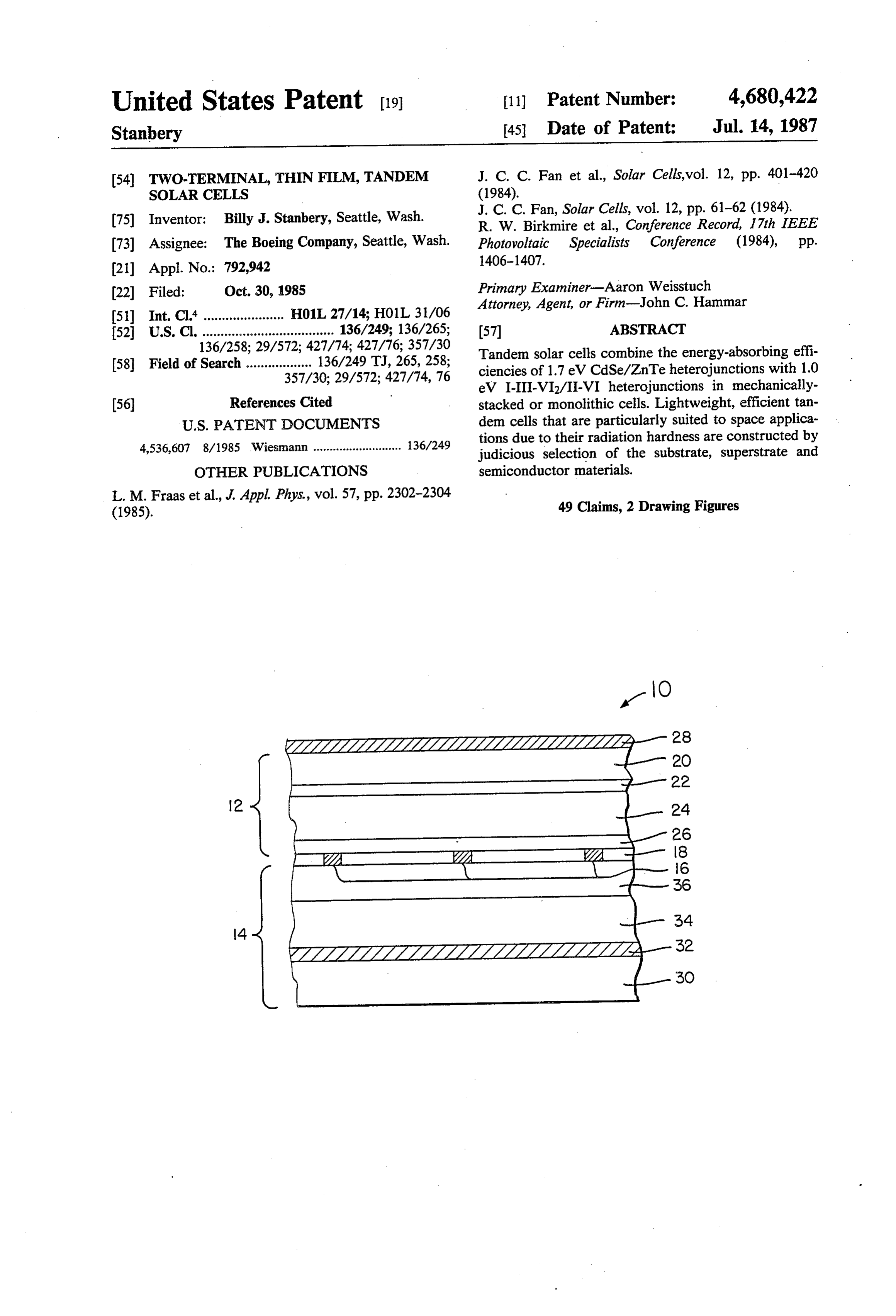
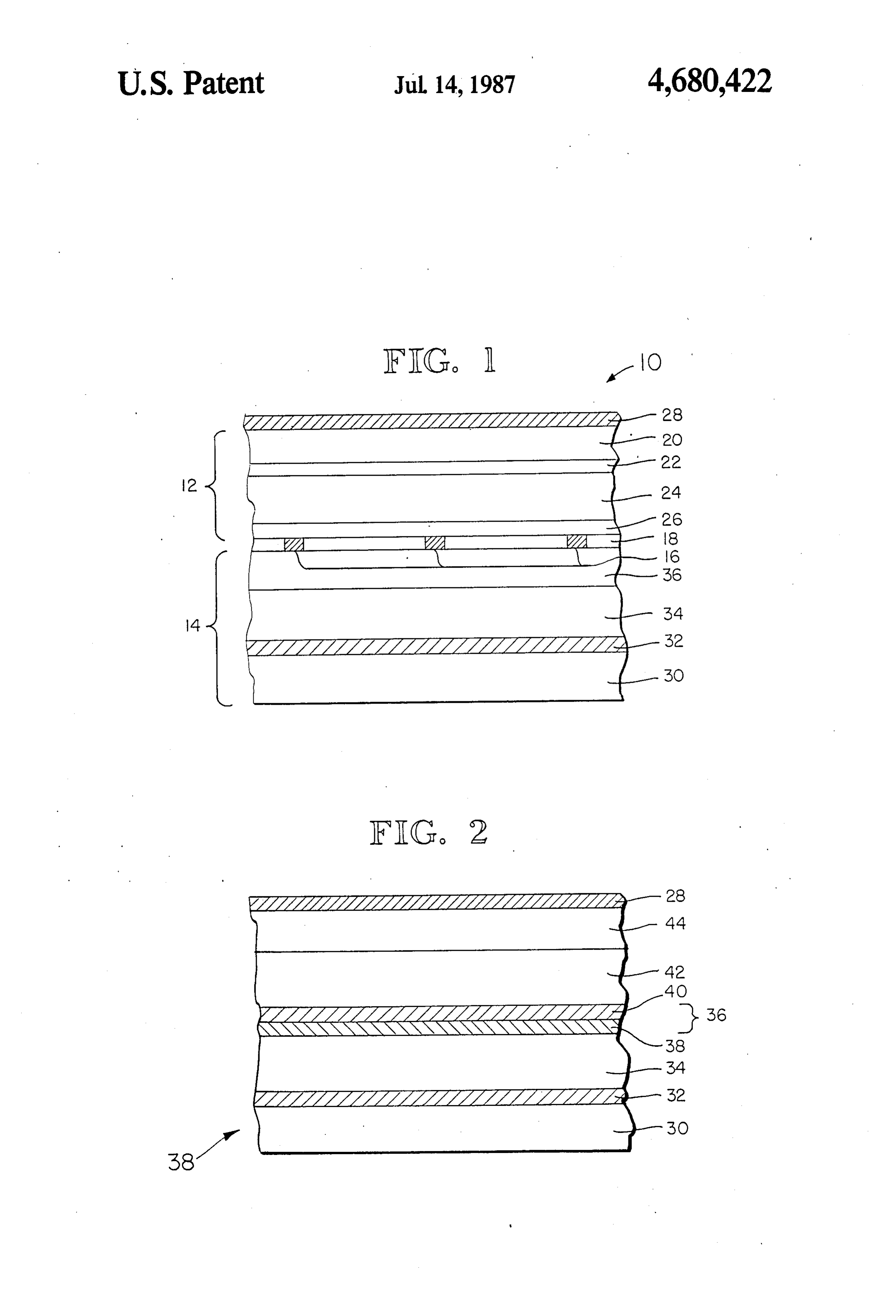
ZnSe-CdTe Heterojunctions, Journal of Luminescence, BRIEF DESCRIPTION OF THE DRAWINGS vol. 15, 109-115 (1977), and Buch et al., Photovoltaic FIG. 1 is a schematic cross-sectional view of a me Properties of n-CdSe/p-ZnTe Heterojunctions, Applied chanically-stacked tandem solar cell of the present in
Neither the I-III-VI2 nor the II-VI cells even as thin FIG. 2 is another schematic cross sectional view of a films independently achieves the goals of weight and monolithic, tandem solar cell, similar to FIG. 1, of the power demanded for space and terrestrial solar cells. present invention.
Solar cells of the present invention, however, combine BEST MODE CONTEMPLATED FOR MAKING these I-III-VI2 and II-VI cells into a mechanically 50 OR USING THE INVENTION stacked or monolithic thin film tandem to achieve a higher efficiency photovoltaic transducer that is partic The present invention relates to mechanically ularly suited for space applications. The cell has surpris stacked or monolithic tandem solar cells or photovol ingly high resistance to radiation damage, is low cost taic transducers, and to methods for making each type due, in part, to polycrystalline structure, and is rela 55 of cell.
tively lightweight due to thin film technology. To simplify the description of these several features of the present invention, this description will be divided
SUMMARY OF THE INVENTION into sections, and reference will be made to the draw The present invention relates to a polycrystalline, ings to aid understanding.
tandem, photovoltaic transducer or solar cell compris 60 1. Mechanically-Stacked Tandem Cell ing an upper cell of a II-VI heterojunction and a lower cell of a graded ternary I-III-VI2 semiconductor. Pref. As shown schematically in FIG. 1, a mechanically erably, the upper cell is an n-type CdSe/p-type ZnTe stacked solar cell or photovoltaic transducer 10 of the heterojunction having aband gap of about 1.7 eV, while present invention includes an upper cell 12 and a lower the lower cell is a CuInSe2 cell having a band gap of 65 cell 14 connected by a metalization grid 16 and a suit about 1.0 eV. able transparent adhesive 18 (if necessary). The metaliz The upper cell generally includes an n-type trans ation grid 16 is preferably formed by copper deposited parent conductive oxide layer contacting the CdSe and on the upper cell 12 and a matching grid of chrome or
Page 4
nickel, and indium on the lower cell. When pressed tion. The rates of evaporation of the several elements, together at an elevated temperature, this metalization is the substrate temperature, and the reactor pressure are probably adequate to hold the cells mechanically and to controlled to achieve high efficiency, polycrystalline interconnect them electrically. An adhesive 18 may be thin films having efficiencies up to about 10% AMO. wicked around the metalization, however, to provide As shown in FIG. 1, the lower cell 14 comprises a more secure mechanical bonding of the cells. The adhe substrate 30 of polycrystalline alumina, glazed alumina, sive 18 should be transparent in the range between enameled steel, metal foil, or a similar inert inorganic about 700-1300 nm (and preferably about 400-1300 material. As suggested by Harry Dursch of The Boeing nm), should adhere to the surfaces of both the top and Company the best substrate 30 for space applications bottom cells, should be easily processable, and should 10 has proven to be a 2-5 mill titanium metal foil. This foil accommodate the differential coefficient of thermal can withstand the high temperatures necessary for fab expansion between the upper and lower cells. While ricating the cell (450° C. for 20 min) without cracking, epoxy adhesives are preferred (if adhesive is used at all), melting, softening, or distorting. When cooled, the foil the adhesive 18 can be selected from the group consist retains its desirable mechanical properties. Titanium foil ing of silicones, ethylvinyl acetates, polyvinyldifluo 15 has a coefficient of thermal expansion that essentially rides, polyimides, or mixtures thereof (if deposited in matches that of the semiconductor material of the cell layers on one cell prior to pressing the cells together). (3.0-5.0x10⁻⁶ in./in./F). This match prevents exces Metalization without adhesive is preferred as the me sive residual stresses or flaking within the cell during chanical interconnect, particularly for space applica thermal cycling between about - 175° C. to 100° C., as tions, since the adhesives can reduce efficiency by ab 20 is experienced in space applications. No outgassing sorbing incident light and can lead to cell failure by occurs from the substrate during deposition. The tita degrading more rapidly than the semiconductors under nium foil is substantially smooth and free of defects or radiation. irregularities. Finally, the foil provides the possibility of a. The upper cell high specific powers (watts/kg) since titanium, espe 25 cially at two mils, is as light a substrate as heretofore
The upper cell 12 comprises several discrete semicon believed possible. Titanium has a density about 50% ductive layers adhered to and deposited on a suitable Less than other suitable substrates, such as molybdenum transparent superstrate 20, generally of alumina or bo foil, and is, accordingly, much lighter. Specific power rosilicate glass or sapphire. The semiconductor layers ratios above 300 watts/kg for arrays are achievable and make the cell 12 into a frontwall drift field cell having a 30 possibly as high as 1000 watts/kg for cells with the II-VI heterojunction. Preferably about 2-10 microme judicious selection of the active semiconductor thin ters of SnO2:F or ZnO:Al is deposited on a sapphire films in the tandem solar cell.
superstrate 20 by CVD or spraying at a temperature of A base contact 32 of molybdenum is deposited over about 350-450 C. as is conventional to form an n the substrate 30 by RF or DC magnetron sputtering. type transparent conductive oxide layer 22. Atop this 35 Then, a graded ternary layer of CuInSe2 is deposited on layer 22, a 3-5 micrometer layer 24 of n-CdSe is depos the contact by reactive evaporation. Improved semi ited by simultaneous elemental reactive evaporation on conductors are formed by controlling the mean free a binary system otherwise analogous to the methods of path between vapor particles in the reactor by increas Mickelsen and Chen described in U.S. Pat. No. Re. ing the pressure to produce a homogenous mixture, as 31,968 and U.S. Pat. No. 4,523,051 (both incorporated 40 described in U.S. Pat. No. 4,523,051. The evaporation by reference), as will be described in greater detail. The rates for Cu and Se should be closely controlled heterojunction is completed thereafter by depositing a throughout the deposition and particularly in the initial layer 26 of p-ZnTe by an enhanced deposition process, deposition of CuInSe2 onto the Mo contact 32, in the such as by reactive evaporation or OMCVD at low bulk of the thin film, and in the region near the junction temperatures below about 350° C. The ZnTe layer 26 is 45 of the film. The substrate temperature should also be doped with phosphorus or copper, and is sufficiently closely controlled throughout the deposition. thick to be uniform, usually about 0.5-3.0 micrometers. The CuInSe2 layer 34 has two different composition If desired, one or more layers 28 of antireflection graded regions sequentially formed with one region coatings, such as SiO, may be adhered to the upper having a first preselected ratio of two elements in the surface of the superstrate 20 to retain incident light and 50 ternary semiconductor material so as to form a low to boost the overall efficiency of the cell. resistivity semiconductor region and the other region Although SnO2:For ZnO:Al on sapphire is preferred having a different preselected ratio of the elements so as for its radiation hardness, the superstrate 20 may be to form a high resistivity transient semiconductor re glass. SnO2:F on glass can be purchased from Chronar gion. The two regions define a transient homojunction. or Nippon glass. A SnO2:halide layer might also be 55 Essentially, one region near the junction is deficient in suitable, but those skilled in the art will recognize the copper while the other region is copper-rich to form a benefits of SnO2:F, which forms the contact for the p-n type heterojunction, as described in detail in U.S. upper cell 12. Pat. No. 31968.
b. The Lower Cell While CulinSe2 is preferred for the lower cell 14, 60 other materials on the I-III-VI2 chalcopyrite semicon
The lower cell i4 preferably is a polycrystalline, thin ductor family might be used, such as a thin-film A-Bfilm, I-III-IV2 chalcopyrite semiconducor, and, more type heterojunction where “A” and 'B' are selected preferably, a p-CulinSe2/n-(Cd,Zn)S heterojunction from the group of semiconductor materials consisting made according to the method of Mickelsen and Chen of:
Briefly, the Mickelsen and Chen method forms a graded, ternary semiconductor free of voids and copper A and B nodules by simultaneous elemental reactive evapora (i) a p-type ternary material and an n-type material;
Page 5
from the substrate 30, if the substrate is a conductive metal foil, such as titanium.
b. The lattice mismatch transition (ii) an n-type ternary and a p-type material;
material The monolithic cell 38 requires an interface connec (iii) an n-type material and a p-type ternary material; tor 36 so that the lattice mismatch between the CuInSe2 (iv) a p-type material and an n-type ternary material.and the upper photoactive layer of the tandem is accom modated. This interface connector 36 has two regions
Compounds of this family include AgInS2, AgCaSe2, 38 and 40 to make the transition in two steps. The first AgGaTe2, AgInSe2, CuGaTe2, AgInTe2, or CuGaS2, 10 transition region 38 is preferably an n-type ZnSe thin but these materials may only have limited application in film window layer deposited by low temperature, solar cells because of their band gaps. plasma enhanched CVD at temperatures no greater The lower cell 14 is completed by depositing a than about 350° C. to avoid detrimental elemental inter (Cd,Zn)S window layer 36 on the CuInSe2 to form a diffusion at the junction. This region is about 0.5-2.0 heterojunction, as explained in the Mickelsen and Chen 15 micrometers thick (preferably about 1.0 micrometers), patents. The resulting cell 14 is a low-cost, polycrystal and is degenerately doped with aluminum in the region line transducer having a conversion efficiency of at least away from the photoactive junction with CuInSe2. Although plasma enhanced deposition is preferred to about 8% AMO, and, preferably over 10% AMO effi reduce ciency when tested apart from the tandem. Efficiencies 20 the films,theit deposition temperatures required to grow is possible to use other enhancement tech of 10.4% AMO have been achieved.
The upper cell 12 preferably has a band gap of about niques, such as OMCVD or laser technologies, to de 1.4-1.6 eV, while the bottom cell 14 has a band gap of posit these films.
Atop the n-ZnSe, a second region 40 of p-ZnTe is about 1.0 eV. To this end, the upper cell may be amor deposited phous silicon, GaAs, CLEFT GaAs, GaAlAs, CLEFT 25 tures. Thisbyregion plasma enhanced CVD at low tempera 40 is about0.5-3.0 microns thick, and
GaAlAs, or the II-VI heterojunction, particularly n is degenerately doped
CdSe/p-ZnTe, described in detail above. The lowest region away from the with upper phosphorus or copper in the photoactive junction.
cost with a surprisingly high resistance to radiation The CuInSe2 to ZnSe lattice mismatch is only about damage and with moderately high efficiencies (leading 2.0% to a specific power in excess of 300 watts/kg) are 30 about and the mismatch between ZnSe/ZnTe is only achievable with the preferred CdSe/ZnTe-CuInSe2 ZnSe/ZnTe Therefore, 0.4%.
is suitable a graded interface layer 36 of to interconnect the CuInSe2 tandem on titanium foil. active layer 34 to the upper layer 42 of CdSe. If other To electrically isolate the contact from the titanium I-III-VI2 chalcopyrites or II-VI heterojunctions are foil substrate in preferred cells, it is desirable to coat the used in the tandem 38, the interface layer 36 should be foil with a dielectric, such as a layer of Si3N4. Radiation 35 selected to achieve this type of smoothly stepped transi resistant cover layers can be added to either the upper tion. Furthermore, the interface connector should be or lower cells to improve their radiation resistance and transparent to energy passing through the upper photo to ease handling of the cells during fabrication of arrays. active layer.
Two mils of FEP-Teflon is adequate for these purposes. The ZnSe/ZnTe layer minimizes the propagation of 2. The Monolithic Cell lattice defects from the lower to the upper junction. Low temperature deposition minimizes dopant redis
As shown in FIG. 2, the present invention also relates tribution within each region, thereby avoiding undesir to a monolithic tandem cell 38 using active semiconduc able reactions at the film interfaces. tor materials similar to the mechanically-stacked cell 10.
Here, however, the layers are sequentially deposited 45 c. The upper photoactive layer upon a single substrate into two photoactive layers The monolithic cell 38 is completed by depositing separated by a lattice mismatch interface connector. n-CdSe, a II-VI semiconductor, in a thin film layer 42 of a. The lower photoactive layer about 3-5 micrometers thickness onto the ZnTe region 40 by reactive evaporation, and then by depositing a
The substrate 30 is identical to that of the lower cell 50 transparent conductive oxide layer 44 of n-type 14 of the mechanically-stacked tandem 10, and, prefera SnO2:For ZnO:Alby CVD or sputtering on the CdSe, bly, is a 2-5 mil sheet of titanium foil, so that the result One or more layers of an antireflection coating 28, such ing transducer has the lightest weight and can withstand as SiO, or MgF2, can be applied above the nt type the severe environment of repetitive thermal cycling in layer 42 to improve cell efficiencies. space. Very high specific powers as already described, 55 The resulting tandem 38 is low-cost, moderately effi can be achieved with titanium foil as compared with cient, polycrystalline, and surprisingly space hardened conventional substrates. against radiation damage. Since no adhesive or metaliz As with the mechanically-stacked cell 10, a thin layer ation is required to interconnect the two photoactive 32 of molybdenum (about 6000A thick) is deposited on layers, the cell is less susceptible to radiation than the the substrate 30 to form a base contact. A graded ter mechanically-stacked tandem 10. Also, the monolithic nary I-III-VI2 semiconductor layer 34 (about 3.0-3.5 cell 38 should be able to withstand thermal cycling micrometers thick) then is deposited by simultaneous better than the mechanically-stacked tandem. reactive elemental evporation on the Mo, according to As described, a CuInSe2/CdSe monolithic cell is the method of Mickelsen and Chen, as previously de preferred, although other I-III-VI2/II-VI cells are pos scribed. This layer 34 preferably is a CuInSe2 thin film 65 sible.
being deficient in copper near the junction so as to be a The interface connector might be a graded p-n type material in the transition from the contact to (Cd,Zn)(S,Se) quarternary material, if desired, and the junction. A Si3N4 dielectric isolates the contact 32 this type of material might also be used to form the
Page 6
junction on the CuInSe2 in the mechanically-stacked 15. The transducer of claim 13 wherein the lower cell tandem, although CdS of CdZnxS is preferred, since is made according to one of the methods of Mickelsen these materials are binaries or ternaries. The quarter and Chen described in U.S. Pat. No. 4,523,051. nary material (Cd,Zn)(S,Se) provides greater flexibil 16. The transducer of claim 13 wherein the lower cell ity in the lattice matching. includes a contact bonded to the CuInSe2 and a sub While preferred embodiments have been shown and strate bonded to the contact.
described, those skilled in the art will readily recognize 17. The transducer of claim 16 wherein the contact alterations, variations, or modifications that might be includes molybdenum.
made to the particular embodiments that have been 18. The transducer of claim 17 wherein the substrate described without departing from the inventive con of the lower cell is a metal foil. cept. This description, the examples, and the drawings 9. The transducer of claim 1 wherein the lower cell are intended to illustrate the invention, and not to limit includes a contact bonded to the I-III-VI2 semiconduc it, unless such limitation is necessary in view of the tor layer and a substrate bonded to the contact. pertinent prior art. Accordingly, the claims should be 15 20. The transducer of claim 19 wherein the substrate interpreted liberally in view of this description to pro of the lower cell is a metal foil.
tect the preferred embodiments of the invention that 21. The transducer of claim 1 wherein the connection have been described and all reasonable equivalents. The between upper and lower cells is metalization between claims should only be limited as is necessary in view of the ZnTe layer and the II-VI semiconductor layer. the pertinent prior art. 22. The transducer of claim 1 further comprising an I claim: adhesive between the upper and lower cells. 1. A polycrystalline, tandem, photovoltaic trans 23. The transducer of claim 22 wherein the adhesive ducer, comprising: is selected from the group consisting of silicones, ethyl (a) an upper cell having a bandgap of about 1.7 eV vinyl acetates, epoxies, polyvinyldifluorides, and polyi and comprising a heterojunction of n-type CdSe 25 mides. 24. The transducer of claim 22 wherein the adhesive and p-type ZnTe, the junction being formed by depositing the ZnTe on the CdSe at low tempera is an 25.
epoxy.
The transducer of claim 22 wherein the adhesive tures below about 350 C.; is substantially optically transparent in the range of (b) a lower cell electrically connected to the upper about 700-1300 nm.
cell, having a bandgap of about 1.0 eV, and com 26. A polycrystalline, thin-film, tandem photovoltaic prising a thin film heterojunction between a graded transducer, comprising:
ternary I-III-VI2 semiconductor and a thin film (a) an upper cell having a bandgap of about 1.7 eV II-VI semiconductor window layer. and comprising:
2. The transducer of claim 1 wherein the upper cell (i) a substantially optically transparent superstrate includes an n-type transparent conductive oxide layer 35 contacting the CdSe. in the range of about 400-1300 nm; 3. The transducer of claim 2 wherein the oxide layer (ii) an in conductive oxide layer deposited on the forms a contact for the upper cell. superstrate, the layer including either SnO2 or 4. The transducer of claim 3 wherein the oxide layer ZnO and having a thickness of between about includes SnO2 or ZnO. 40 2-10 micrometers; and 5. The transducer of claim 4 wherein the oxide layer (iii) a frontwall heterojunction comprising about a includes SnO2:F. 3-5 micrometer layer of CdSe deposited on the 6. The transducer of claim 2 wherein the upper cell oxide layer and about a 0.5-3 micrometer layer includes a substantially optically transparent super 45 of ZnTe deposited on the CdSe at a temperature at or below about 350° C. to control and limit strate, transparent in the range between about 400-1300 CdSe-ZnTe interdiffusion at the heterojunction; nm, bonded to the oxide layer. (b) a lower cell having a bandgap of about 1.0 eV and 7. The transducer of 6 wherein the lower cell semi comprising:
conductors include a CuInSe2/(Cd,Zn)S heterojunc (i) a substrate;
tion. (ii) a molybdenum contact layer deposited on the 8. The transducer of claim 7 wherein the lower cell 50 substrate; and includes a contact and a substrate bonded to the (iii) a graded CuInSe2/(Cd,Zn)S semiconductor COntact. heterojunction deposited on the contact layer; 9. The transducer of claim 8 wherein the contact and includes molybdenum. 55 (c) metalization connecting the upper and lower cells 10. The transducer of claim 9 wherein the substrate of between the ZnTe layer of the upper cell and the lower cell is a metal foil. (Cd,Zn)S layer of the lower cell. 11. The transducer of claim 10 wherein the foil is 27. The transducer of claim 26 further comprising a titanium. substantially optically transparent adhesive in the range 2. The transducer of claim 7 wherein the connection 60 between about 700-1300 mm for bonding the upper and between the upper and lower cells is metalization be lower cells.
tween the ZnTe layer and the (CdZn)S layer. 28. The transducer of claim 26 wherein the oxide 13. The transducer of claim wherein the lower cell layer includes SnO2:F.
semiconductors include a CuInSe2/(Cd, Zn)S hetero 29. The transducer of claim 26 wherein the lower cell junction. 65 is made according to one of the methods of Mickelsen 14. The transducer of claim 3 wherein the lower cell and Chen described in U.S. Pat. No. Re. 31,968. is made according to one of the methods of Mickelsen 30. The transducer of claim 26 wherein the substrate and Chen described in U.S. Pat. No. 31,968. is titanium foil.
Page 7
31. The transducer of claim 30 wherein the super (e) an n-CdSe layer having a bangap of about 1.7 eV strate is either glass or sapphire. deposited on the p-ZnTe of the interface layer; and 32. A polycrystalline, thin-film, tandem, photovoltaic (f) a transparent conductive oxide upper contact de transducer, especially adapted for terrestrial and space posited on the n-CdSe layer. solar cell applications, comprising: 5 44. The transducer of claim 43 further comprising an (a) a polycrystalline p-ZnTe/n-CdSe/n conductive antireflection coating bonded to the upper contact. oxide frontwall heterojunction drift field cell as the 45. A method of making a monolithic, polycrystal upper cell of the tandem; and line, tandem, photovoltaic transducer, comprising the (b) a thin-film, I-III-VI2/II-VI heterojunction as the steps of:
lower cell of the tandem, the lower cell being char 10 (a) applying a metallic base contact to a suitable sub acterized as without voids or copper nodules and strate;
having an energy conversion efficiency, when (b) sequentially depositing a graded p-CuInSe2 layer tested apart from the tandem, of a least about 8% on the contact, the layer having two regions, a first AMO. region on the contact and a second region away 33. The transducer of claim 32, exhibiting superior 15 from the contact atop the first region, the regions radiation hardness characteristics, low weight, and high being formed by the simultaneous elemental evapo energy conversion efficiency, further comprising: ration of Cu, In, and Se, the region away from the (a) a substantially optically transparent sapphire su contact being slightly copper deficient so as to perstrate for the upper cell; form a moderately high resistivity, transient n-type (b) a titanium metal foil substrate for the lower cell; 20 (c)layer; depositing n-ZnSe on the n-type CuInSe2 layer by (c) a molybdenum contact deposited over the foil beneath the heterojunction; and low temperature CVD to avoid interdiffusion at (d) a dielectric between the foil and contact. the junction;
34. The transducer of claim 33 wherein the lower cell (d) depositing p-ZnTe on the n-ZnSeby low temper heterojunction is graded CuInSe2/(Cd,Zn)S. 25 ature CVD to avoid interdiffusion at the junction, 35. The transducer of claim 34 wherein the upper cell the n-ZnSe and p-ZnTe forming an interface transi has a bandgap of about 1.7 eV and the lower cell has a tion between the lattice of the CuInSe2 layer and an bandgap of about 1.0 eV. upper cell, and being degenerately doped in the 36. A monolithic, polycrystalline, tandem, photovol regions away from the photoactive junctions; taic transducer, comprising: 30 (e) depositing n-CdSe to form the upper cell on the (a) a lower cell comprising a I-III-VI2 semiconductor p-ZnTe; and photoactive layer having a bandgap of about 1.0 (f) depositing an upper contact of n-type transpar eV; ent conductive oxide on the n-CdSe. (b) a graded interface connector deposited on the 46. The method of claim 45 further comprising the lower cell to provide a smooth lattice match transi step of applying an antireflection coating to the upper tion between the lower cell and an upper cell of the 35 COntact.
tandem, the connector being degenerately doped in 47. The method of claim 45 wherein the p-CulnSe2 the regions away from the photoactive junctions; layer has abandgap of about 1.0 eV and then-CdSe has and a bandgap of about 1.7 eV.
(c) a polycrystalline n-type CdSe/n, transparent 40 48. A method for making a polycrystalline, tandem, conductive oxide cell deposited sequentially atop photovoltaic transducer, comprising the steps of: the connector to form the upper cell, the upper cell (a) forming a lower cell by the steps of: having a bandgap of about 1.7 eV. (i) depositing a molybdenum contact over a metal 37. The transducer of claim 36 wherein the lower cell foil substrate;
photoactive layer includes CuInSe2. (ii) depositing a graded p-n type CunSe2 layer on 38. The transducer of claim 36 wherein the interface 45 the contact by simultaneous elemental evapora connector includes n-ZnSe/p-ZnTe. tion, the layer having a portion removed from 39. The transducer of claim 36 wherein the lower cell the contact that is copper-deficient, and having a includes a molybdenum contact deposited on a substrate bandgap of about 1.0 eV; below the photoactive layer. (iii) depositing an n-(Cd,Zn)Slayer atop the Culin 40. The transducer of claim 39 wherein the substrate 50 Se2 layer;
is a metal foil, and the cell further comprises a dielectric (b) forming an upper cell by the steps of: between the foil and contact. (i) depositing an n-type transparent conductive 41. The transducer of claim 40 wherein the foil is oxide layer on a glass or sapphire superstrate; titanium. (ii) depositing a layer of n-CdSe by reactive evapo 42. The transducer of claim 36 further comprising an 55 ration on the n-type layer; and antireflection coating bonded to the transparent con (iii) depositing a layer of p-ZnTe at low tempera ductive oxide. tures on the n-CdSe to avoid interdiffusion at the 43. A monolithic, polycrystalline, tandem, photovol junction;
taic transducer, comprising: (c) applying metalization to either the ZnTe or (a) a metal foil substrate; 60 (Cd/Zn)S; and (b) a molybdenum contact deposited over the sub (d) pressing the upper and lower cells together under strate; suitable heat to bond the upper and lower cells (c) a p-CulnSe2 layer having a bandgap of about 1.0 together through the metalization. eV deposited on the contact; 49. The method of claim 48 further comprising the (d) a graded n-ZnSe/p-ZnTe interface connector 65 step of applying a substantially optically transparent deposited upon the p-CunSe2 layer, the interface adhesive to the upper and lower cells around the metal layer being degenerately doped in the regions away ization. st k k from the photoactive junctions;
Provenance
- Collection
- Cited prior art
- Original PDF
- patentimages.storage.googleapis.com →
- Filed
- 1985-10-30
- Pages
- 7
- Method
- pdftotext (the PDF's own text layer) + pdftoppm 300dpi page scans
- Source
- Google Patents bibliographic record
- Granted
- 1987-07-14
- Inventors
- Billy J. Stanbery; Boeing Co
- Transcribed from
- patentimages.storage.googleapis.com →