patent · US5009719
Tandem solar cell
23 April 1991
Page 1 — bibliographic record
United States Patent (19) 11 Patent Number: 5,009,719 Yoshida 45 Date of Patent: Apr. 23, 1991 (54) TANDEM SOLAR CELL 62-14110 3/1987 Japan ................................... 136/249 (75) Inventor: Susumu Yoshida, Hyogo, Japan OTHER PUBLICATIONS 73) Assignee: Mitsubishi Denki Kabushiki Kaish L. M. Fraas et al., Conference Record, 16th IEEE Photo Japan voltaic Specialists Conference (1982), pp. 655-662. 21 Appl. No.: 433,278 S. M. Vernon et al., Conference Record, 17th IEEE Photovoltaic Specialists Conference (1984), pp. 434-439.
(22 Filed: Nov. 8, 1989 H. C. Hamaker, Conference Record, 18th IEEE Photoyol (30) Foreign Application Priority Data taic Specialists Conference (1985), pp. 140-145. Feb. 17, 1989 (JP) Japan .................................... 1-38691 "High Efficiency AlGaAs/GaAs Tandem Solar Cells Grown by Molecular Beam", Int'l PVSEC-3, pp.
51) Int. C. ........................................... H01L 31/068 772-774.
52 U.S.C. ....................................... 136/249; 357/30 Primary Examiner-Aaron Weisstuch 58 Field of Search .................. 136/249 TJ; 357/30 J Attorney, Agent, or Firm-Leydig, Voit & Mayer 56 References Cited (57) ABSTRACT
A tandem solar cell device includes an upper solar cell, 4,575,577 3/1986 Fraas............................ 136/249 TJ a lower solar cell, and an intervening buffer layer. A 4,631,352 12/1986 Daud et al. .................... 136/249 TJ short wavelength region of the incident light is ab 4,680,422 7/1987 Stanbery. . . 136/249 TJ sorbed by the upper solar cell while the light having 4,681,982 7/1987 Yoshida ... ... 136/249 passed through the upper solar cell is absorbed by the
lower solar cell. The buffer layer is a semiconductor
FOREIGN PATENT DOCUMENTS layer having a larger band gap energy than the upper 57-1268 l/1982 Japan ................................... 136/249 solar cell, a crystalline lattice match with the upper 58-119676 7/1983 Japan ........... ... 36/249 solar cell, and a tunnel junction. 58-119679 7/1983 Japan ................................... 36/249 58-127386 7/1985 Japan ............................. 136/249 TJ 9 Claims, 4 Drawing Sheets
Page 2
Drawing sheet — no readable text.
Page 3
Drawing sheet — no readable text.
Page 4
Drawing sheet — no readable text.
Page 5
Drawing sheet — no readable text.
Page 6
tween the p-type Silayer 12 and the GaAs layer 21,
TANDEM SOLAR CELL thereby improving the crystallinity of the GaAs. Fur thermore, in order to improve the electrical junction
FIELD OF THE INVENTION between the upper GaAs solar cell 20 and the lower Si The present invention relates to a tandem solar cell solar cell 10, the buffer layer 30 includes a p-type Ge device and, more particularly, to a buffer layer inserted layer 31 and an n-type Gelayer 32 containing a high between solar cells of a tandem solar cell device includ concentration of dopant impurities and a tunnel junc ing different kinds of solar cells. tion 30a is produced within the buffer layer 30. BACKGROUND OF THE INVENTION 10 The energy band gap of the Ge buffer layer 30 is narrower than that of Si, i.e., the band gap energy of Si
A tandem structure solar cell device comprising a is 1.11 eV while that of Ge is 0.66 eV. As a result, light GaAs solar cell serially disposed on a Si solar cell uti that can be converted into electricity by the Silayer is lizes solar light more effectively than either a Si solar absorbed by the Gebuffer layer 30 and hardly reaches cell or a GaAs solar cell alone.
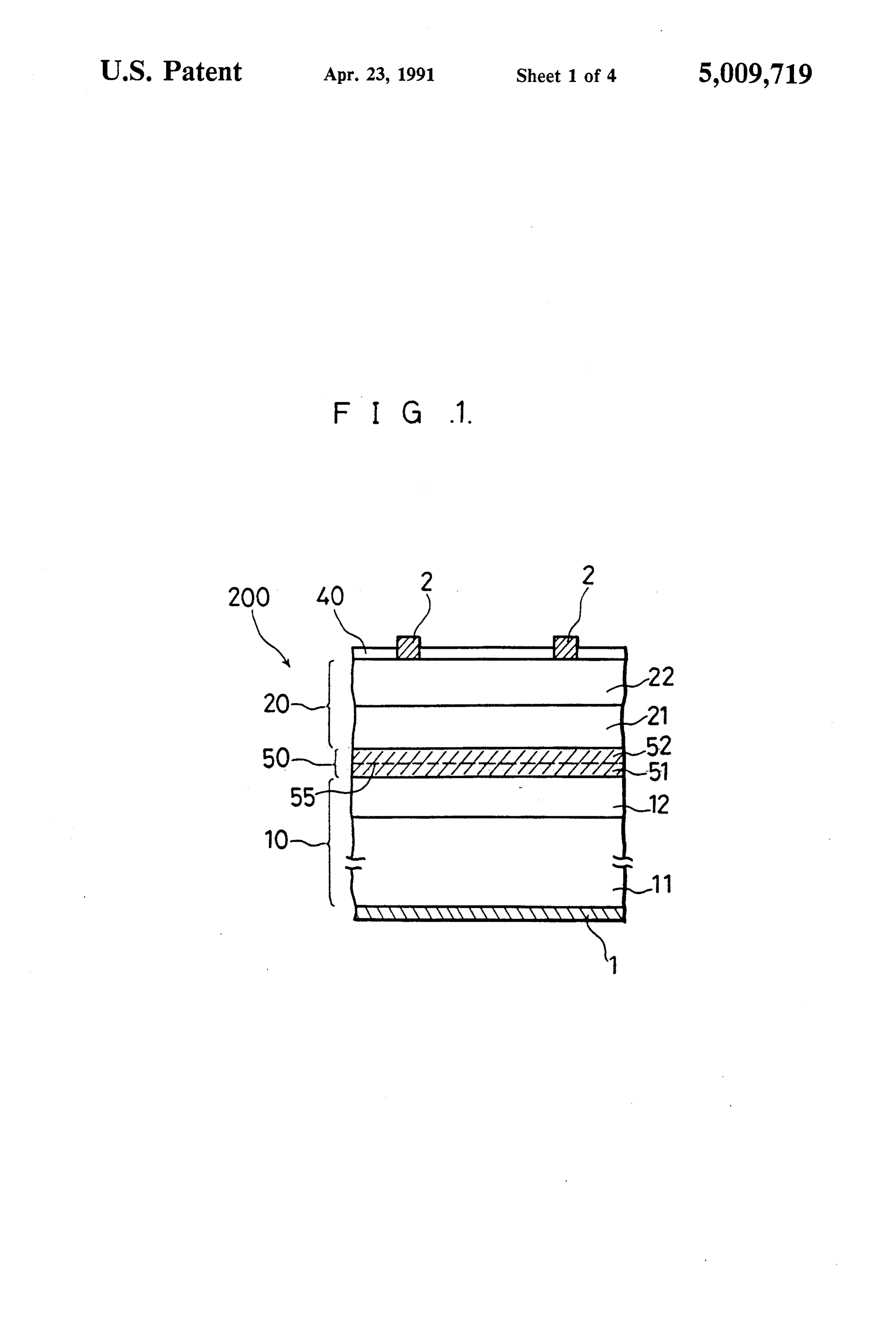
FIG. 2 is a cross-sectional view of a prior art tandem version takescellplace 15 the Sisolar 10; that is, the light-to-electricity con not in the Silayer having a high solar cell device. In FIG. 2, a Sisolar cell (lower solar light-to-electricity conversion efficiency but in the Ge cell) 10 includes an n-type Si substrate 11 about 100 to 200 microns thick and a p-type Silayer 12 less than 1 layer having a low light-to-electricity conversion effi micron thick disposed thereon. Light having wave 20 ciency. This lowers the light-to-electricity conversion lengths of 0.4 to 1.1 microns is absorbed by and con efficiency of the entire device.
verted to electricity by the Sisolar cell 10. A GaAs SUMMARY OF THE INVENTION solar cell (upper solar cell). 20 includes an n-type GaAs layer 21 about 2 microns thick and a p-type GaAs layer It is an object of the present invention to provide a 22 about 1 micron thick disposed thereon. Light having 25 tandem solar cell device having an upper solar cell with wavelengths of 0.4 to 0.9 microns is absorbed by and improved crystallinity without reducing the light trans converted to electricity by the GaAs solar cell 20. A missivity of a buffer layer disposed between the upper buffer layer 30 less than several hundred angstroms and lower solar cells.
thick is inserted between the upper solar cell 20 and the It is another object of the present invention to pro lower solar cell 10, improving the lattice matching of vide a tandem solar cell device having a high efficiency the Si and GaAs crystals. This buffer layer 30 includes which includes an improved electrical connection be
a tunnel junction 33 and a high impurity concentration tween the upper and the lower solar cells. p+-type Gelayer 31 and an n-type Gelayer 32 sand It is still another object of the present invention to wiching the tunnel junction. provide a method of producing such a tandem solar cell An n side ohmic contact electrode 1 is disposed on the rear surface of the n-type Si substrate 11. A p side 35 device.
Other objects and advantages of the present invention ohmic contact electrode 2 is disposed on part of the front surface of the p-type GaAs layer 22. An anti will become apparent from the detailed description reflection film 40 comprising a silicon nitride film hav given hereinafter. It should be understood, however, ing a thickness of 600 to 700 angstroms is disposed o that the detailed description and specific embodiments the exposed surface of GaAs layer 22. are given by way of illustration only, since various Thus, a tandem solar cell device 100 includes the changes and modifications within the spirit and scope of upper solar cell 20, the lower solar cell 10, the buffer the invention will become apparent from the detailed layer 30, the anti-reflection film 40, the p side electrode description.
2, and the n side electrode 1. According to an aspect of the present invention, a In the tandem solar cell device described, light of 45 buffer layer is inserted between an upper solar cell and relatively short wavelengths, i.e., of 0.4 to 0.9 microns, a lower solar cell of a tandem solar cell device for im from the solar light spectrum of 0.4 to 2 micron wave proved lattice matching of the crystals of the solar cell lengths which is incident on the device from above is converted into electricity by the upper GaAs solar cell layers.
material
This buffer layer comprises a semiconductor having a larger energy band gap than that of a 20, and the light that passes through the upper solar cell 50 semiconductor 20 is converted into electricity by the lower Sisolar cell which enhancesmaterial the comprising the upper solar cell light transmissivity of the buffer 10. The charge carriers generated at the respective solar layer without adversely affecting cells 10 and 20 are extracted through the electrodes 1 upper solar cell. Thus, the solar the crystallinity of the light will not be ab and 2 as a photocurrent that passes through the thin sorbed by the buffer layer and is effectively converted buffer layer 30 disposed between the two solar cells. 55 to electricity by the lower solar cell. In the prior art tandem solar cell device, the lattice Since a tunnel junction is disposed within the buffer matching buffer layer 30 cuts off light which could be layer, an improved electrical connection is realized converted to electricity by the lower solar cell 10 and little electricity is produced in the lower solar cell 10. between the upper solar cell and the lower solar cell, In more detail, when a plurality of semiconductor thereby reducing the resistance loss which would other layers, having different lattice constants are serially wise occur at the junction.
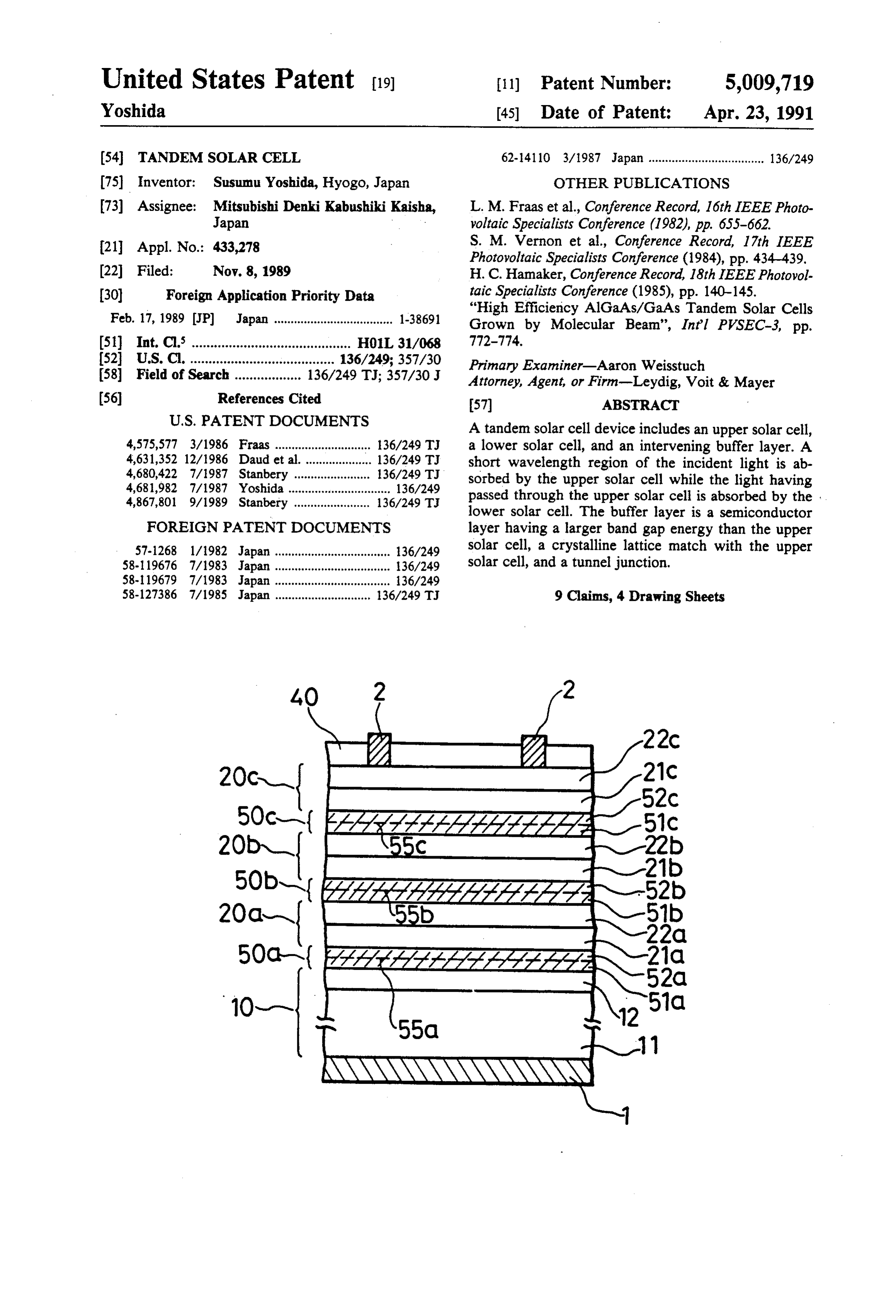
disposed, crystalline defects are produced and a semi BRIEF DESCRIPTION OF THE DRAWINGS conductor layer of good crystallinity cannot be ob tained. The movement of charge carriers in the semi FIG. 1 is a cross-sectional view of a tanden solar cell conductor layer is obstructed by the crystalline defects, 65 device according to a first embodiment of the present thereby decreasing device efficiency. Therefore, in this invention;
prior art device, the Gebuffer layer 30 whose crystal FIG. 2 is a cross-sectional view of a prior art tandem lattice constant matches that of GaAs is inserted be solar cell device;
Page 7
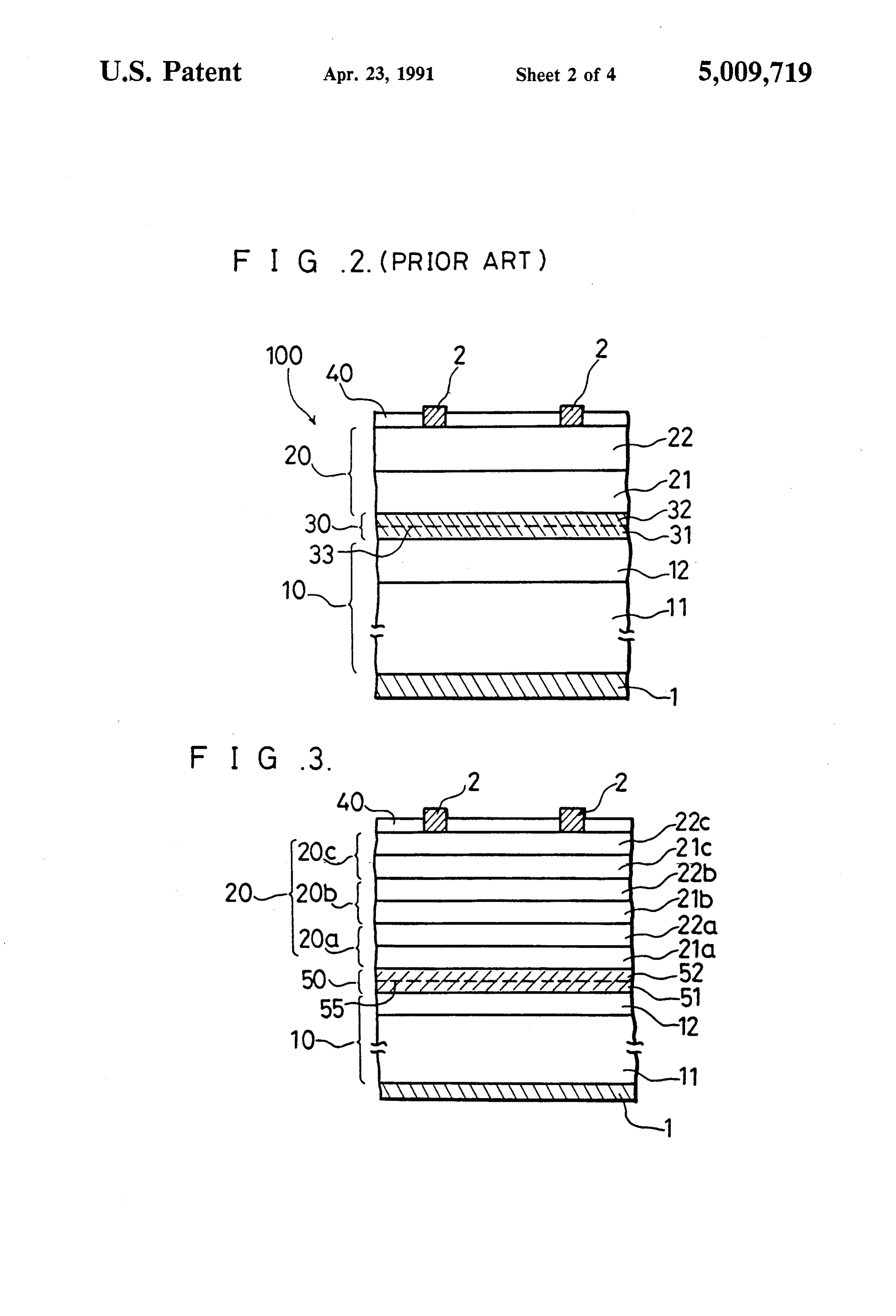
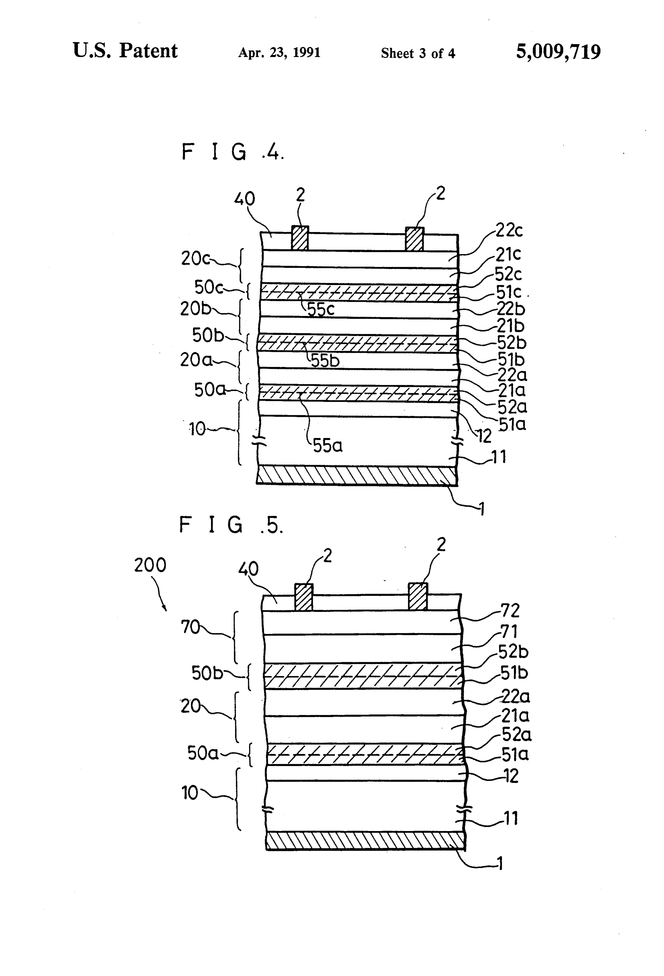
FIG. 3 is a cross-sectional view of a tandem Solar cell which produces an improved electrical connection be device according to a second embodiment of the pres tween the solar cells.
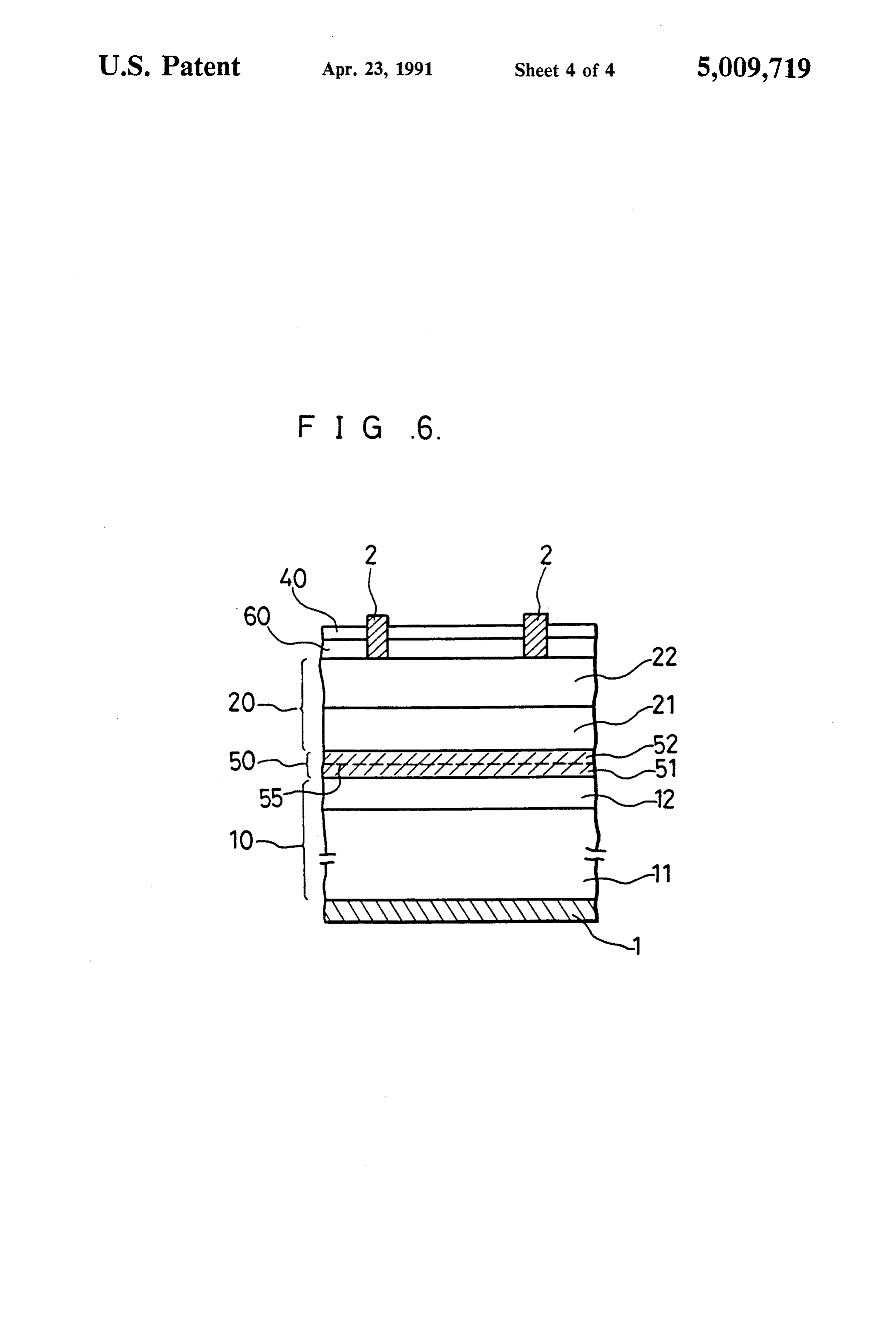
ent invention; Next, an n-type GaAs layer 21 having a carrier con FIG. 4 is a cross-sectional view of a tandem solar cell centration of 1X 10 cm and containing Se or S as a device according to a third embodiment of the present dopant and a p-type GaAs layer 22 having a carrier invention; concentration of 5X 10 cm and containing Zn as a FIG. 5 is a cross-sectional view of a tandem solar cell dopant are successively grown on the ZnSe buffer layer device according to a fourth embodiment of the present 50 to thicknesses of 1.5 to 3 microns and 0.5 microns, invention; and respectively, by MOCVD using trimethylgallium FIG. 6 is a cross-sectional view of a tandem solar cell 10 (TMGa) and arsine (AsH3) to form the upper solar cell device which is obtained by providing a window layer 20. The conditions of this MOCVD process are a in the device of FIG. 1. growth temperature of 750° C. and a pressure of about
DETAILED DESCRIPTION OF THE Thus, the light-to-electricity regions, i.e., the silicon PREFERRED EMBODIMENTS 15 solar cell 10 and the GaAs solar cell 20, are produced. FIG. 1 is a cross-sectional view of a tandem solar cell Thereafter, a silicon nitride (Si3N4) film 40 as an anti device according to a first embodiment of the present reflection film is deposited on the p-type GaAs layer 22 invention. In FIG. 1, a tandem solar cell device 200 to a thickness of 700 to 800 angstroms by a plasma CVD includes a lower Si solar cell 10 and an upper GaAs method or by thermal decomposition of silane gas and solar cell 20 disposed thereon. The lower Sisolar cell 10 20 ammonia gas at 700 C.
Thereafter, a titanium layer, which has good adhe includes an n-type Sisubstrate 11 having a resistivity of 2 ()ocm, a thickness of 200 microns, and a diameter of 3 sion to semiconductors, is deposited on the rear surface of Si substrate 11 as well as on the front surface of inches, and a p-type Sidiffusion layer 12 having a thick p-type GaAs layer 22 to a thickness of about 500 ang ness of 0.15 to 0.3 micron disposed on the Si substrate.
A buffer layer 50 of a semiconductor material having a 25 stroms tering.
by electron beam deposition (MBE) or by sput
Subsequently, silver is deposited on the Tilayers larger band gap energy than that of GaAs comprising the upper solar cell 20 is disposed on the p-type Silayer to a thickness of several microns by electron beam de 12. Herein, ZnSehaving a band gap energy of 2.67 eV, position for connection with the external lead terminals, larger than the band gap energy of GaAs, i.e., 1.43 eV, 30 forming a p side ohmic contact electrode 2 on the p is used for the buffer layer. This buffer layer 50 includes type GaAs layer 22 and an in side ohmic contact elec a p-type ZnSe layer 51 and an n+-type ZnSelayer 51 trode 1 on the n-type Si substrate 11. In this embodiment, since a ZnSe buffer layer 50 comprising a tunnel junction. The upper solar cell 20 having comprising III-V compound semiconductors including layer is ainserted larger energy band gap than that of the GaAs between the lower Sisolar cell 10 and
GaAs includes an n-type GaAs layer 21 about 1.5 to 3 35 the upper GaAs solar cell 20, the long wavelength light microns thick and a p-type GaAs layer 22 about 0.5 which can be converted to electricity by the Silayer 10 micron thick. The other elements are the same as those of FIG. 2. is not absorbed by the buffer layer 50. Thus, since the In this embodiment, when light, such as solar light, is ZnSe buffer layer 50 has a band gap energy of 2.67 eV, incident on the device from above, light of relatively larger than that of silicon, and is transparent in a long wavelength region, the long wavelength light is inci short wavelengths is absorbed by the pnjunction of the dent on the lower solar cell 10 and is converted to elec n-type GaAs layer 21 and the p-type GaAs layer 22, and tricity with high efficiency.
the light of relatively long wavelengths which has Since ZnSe matches GaAs in lattice constant, no passed through the GaAs layer 20 and the ZnSe buffer crystal defects are created during crystal growth of the layer 50 is converted to electricity by the pnjunction of 45 GaAs layer on the ZnSebuffer layer 50, and a relatively the n-type Sisubstrate 11 and the p-type Silayer 12. The perfect GaAs crystalline structure can be obtained. charge carriers generated at the respective solar cells 20 Therefore, the charge carriers at the upper GaAs solar and 10 are extracted from then side electrode 1 and the cell 20 have a higher degree of freedom in their move p side electrode 2 as a photocurrent through the ZnSe ment, which increases efficiency.
layer 50. 50 Furthermore, since a tunnel junction 55 is produced To construct the tandem solar cell device 200, the inside the ZnSe buffer layer 50, the electrical junction surface of the Si substrate 11 is treated with an acid between the lower Sisolar cell 10 and the upper GaAs mixture (a solution of sulfuric acid and aqua regia) solar cell 20 is improved, thereby reducing the resis which is well known as an etchant for Si. Thereafter, a tance loss which would otherwise occur at the junction. p-type Sidiffusion layer 12 having a thickness of 0.15 to 55 As a result, the light-to-electricity conversion efficiency 0.3 micron is produced by a thermal diffusion using of the entire device is improved.
BBr3 as a diffusion source at a diffusion temperature of In the above-illustrated embodiment, a ZnSe layer 1050' C. and a diffusion time of 40 to 60 minutes. having a larger energy band than that of the BaAs layer Next, a p-type ZnSe layer 51 and an n-type ZnSe of the upper solar cell 20 is used, but an AlGaAs layer layer 52 having carrier concentrations of about having a larger band gap energy than that of GaAs may 10 cm are successively grown to thickness of 500 to be used.
1000 angstroms on the Si substrate 11 by the metal While in the above-illustrated embodiment the upper organic chemical vapor deposition (MOCVD) process solar cell 20, is GaAs, it may be an AlxGa1-xAs using dimethylzinc (DMZn) and hydrogen selenide (0<x) l) layer. In this case, a high quality crystal can (H2Se) to form the buffer layer 50. The MOCVD tem 65 be produced not only on the AlGaAs buffer layer but perature is 300° C. and the pressure is 0.4 Torr. The also on the ZnSe buffer layer.
ZnSe layer 50 produces a tunnel junction between the As shown in FIG. 6, when a window layer 60 of lower Si solar cell 10 and the upper GaAs solar cell 12 AlxGa1-xAs (x=0.8 to 0.9) is disposed on the p-type
Page 8
GaAs layer 22 of GaAs solar cell 20, surface recombina layer 71 and a p-type AlGaAs layer 72 disposed tion due to defects at the surface of the GaAs layer can thereon. The second buffer layer 50b includes a p-type be reduced. This window layer 60 is grown to a thick AlGaAs layer 51b and an n-type AlGaAs layer 52b. ness of below 0.1 micron in order to suppress the ab Herein, a pit-type GaAs layer may be used in place of sorption of short wavelength light therein. This win the pt-type AlGaAs layer 51b. dow layer 60 can be produced successively without In the upper auxiliary AlGaAs solar cell 70, the range semiconductor layers using a method similar to the of wavelengths that can be absorbed is increased production method for the GaAs cell, that is, MOCVD, toward the shorter wavelengths, i.e., to a range of 0.3 to MBE, or liquid phase epitaxy (LPE). 0.9 micron, compared to a range of 0.4 to 0.9 micron for While in the above-illustrated embodiment the tan O the upper solar cell 20. Therefore, the natural short dem solar cell device 200 has a single upper solar cell wavelength light can be effectively converted to elec 20, a plurality of light-to-electricity conversion regions tricity, thereby improving the conversion efficiency. may be produced as an upper solar cell. Such a light-to Furthermore, the resistance loss at the electrical junc electricity conversion device having an upper solar cell tion between the main and auxiliary solar cells can be including a tandem structure is described according to 15 suppressed.
second and third embodiments of the present invention.
FIG. 3 shows a tandem solar cell device according to ingAstoisthe evident from the foregoing description, accord a second embodiment of the present invention. In FIG. matching ispresent inserted invention a buffer layer for lattice between an upper cell and a lower 3, an upper solar cell 20 is obtained by successively cell of a tandem solar depositing first to third AlxGa1-xAs light-to-electricity 20 includes a semiconductorcell device. This buffer layer material having a larger band conversion regions 20a to 20c on a ZnSe buffer layer 50. gap energy than that of the semiconductor material in The farther from the buffer layer 50 the AlxGa1-xAs the upper solar cell and includes a tunnel junction. light-to-electricity conversion region is, the larger the
Al composition ratio x is. These regions 20a, 20b, and Therefore, the solar the crystallinity of the upper solar cell and light permeability of the buffer layer are im 20c respectively include p-type AlxGa1-xAs layers 21a, 25 proved. Furthermore, 21b, 21c and n-type AlxGa1-xAs layers 22a, 22b, 22c. tunnel junction, a goodsince the buffer layer includes a electrical junction between the
The other elements are the same as in FIG. 1.
respective light-to-electricity conversion regions is real
In this device, in addition to the effects of the above ized, described first embodiment, the light-to-electricity con otherwise thereby reducing the resistance loss which would version efficiency of the upper solar cell 20 is enhanced; 30 the occur at the respective junctions. As a result, that is, the solar light which has passed through region device total light-to-electricity conversion efficiency of the 20c or 20b without being absorbed can be absorbed by is improved.
the lower region 20b or 20a, respectively. Therefore, What is claimed is:
light-to-electricity conversion can be effectively 1. A tandem solar cell including: achieved for the short wavelength components of solar 35 an upper solar cell for converting relatively short light. Furthermore, the respective light-to-electricity wavelength incident light into electricity, compris conversion regions can be easily produced by varying ing a first crystalline semiconductor having a first the composition ratio of AlGaAs during its growth. lattice constant and first energy band gap; FIG. 4 shows a tandem solar cell device according to an intermediate solar cell for converting relatively a third embodiment of the present invention. In this long wavelength incident light that has passed device, in addition to the first ZnSe buffer layer 50 through said upper solar cell into electricity, com disposed between the lower solar cell 10 and the upper prising a second crystalline semiconductor having solar cell 20, second and third ZnSe buffer layers 50b a second energy band gap smaller than the first and 50c are disposed between the respective light-to energy band gap;
electricity conversion layers of upper solar cell 20. The 45 lower solar cell for converting relatively long respective buffer layers 50a to 50c include respective wavelength incident light that has passed through tunnel junctions 55a to 55c including first to third int said intermediate solar cell into electricity, com type ZnSe layers 52a to 52c and first to third pt-type prising a third crystalline semiconductor having a ZnSe layers 51a to 51c, respectively. Herein, the buffer third energy band gap smaller than the second layer may comprise AlGaAs instead of ZnSe. 50 energy band gap; and
In this embodiment, the electrical junction between crystalline semiconductor buffer layers respectively the respective light-to-electricity conversion regions disposed between said upper and intermediate solar can be improved whereby the resistance loss at the cells and between said intermediate and lower solar junction can be reduced and the light-to-electricity cells, each buffer layer having an energy band gap conversion efficiency can be enhanced relative to the 55 larger than the first energy band gap and a lattice second embodiment. constant approximately the same as the first lattice While in the above-described second and third em constant and including a tunneling junction within bodiments, the same semiconductor material is used for each of said buffer layers. the multilayer light-to-electricity conversion regions of 2. The tandem solar cell of claim 1 wherein said the upper solar cell, GaAs may be used as the main 60 lower solar cell comprises silicon and said intermediate light-to-electricity conversion region and AlGaAs may and upper solar cells comprises a III-V compound semi be used as the auxiliary light-to-electricity conversion conductor including Ga and As.
regions. 3. The tandem solar cell of claim 2 wherein said upper FIG. 5 shows a tandem solar cell according to a solar cell comprises AlxGa1-xAs.
fourth embodiment of the present invention. In FIG. 5, 65 4. The tandem solar cell of claim 2 including a win an upper auxiliary AlGaAs solar cell 70 is disposed on dow layer comprising an AlxGa1-xAs layer, where x is the GaAs solar cell 20 with a second buffer layer 50b. 0.8 to 0.9, disposed on said upper solar cell for receiving The AlGaAs solar cell 70 includes an n-type AlGaAs incident light.
Page 9
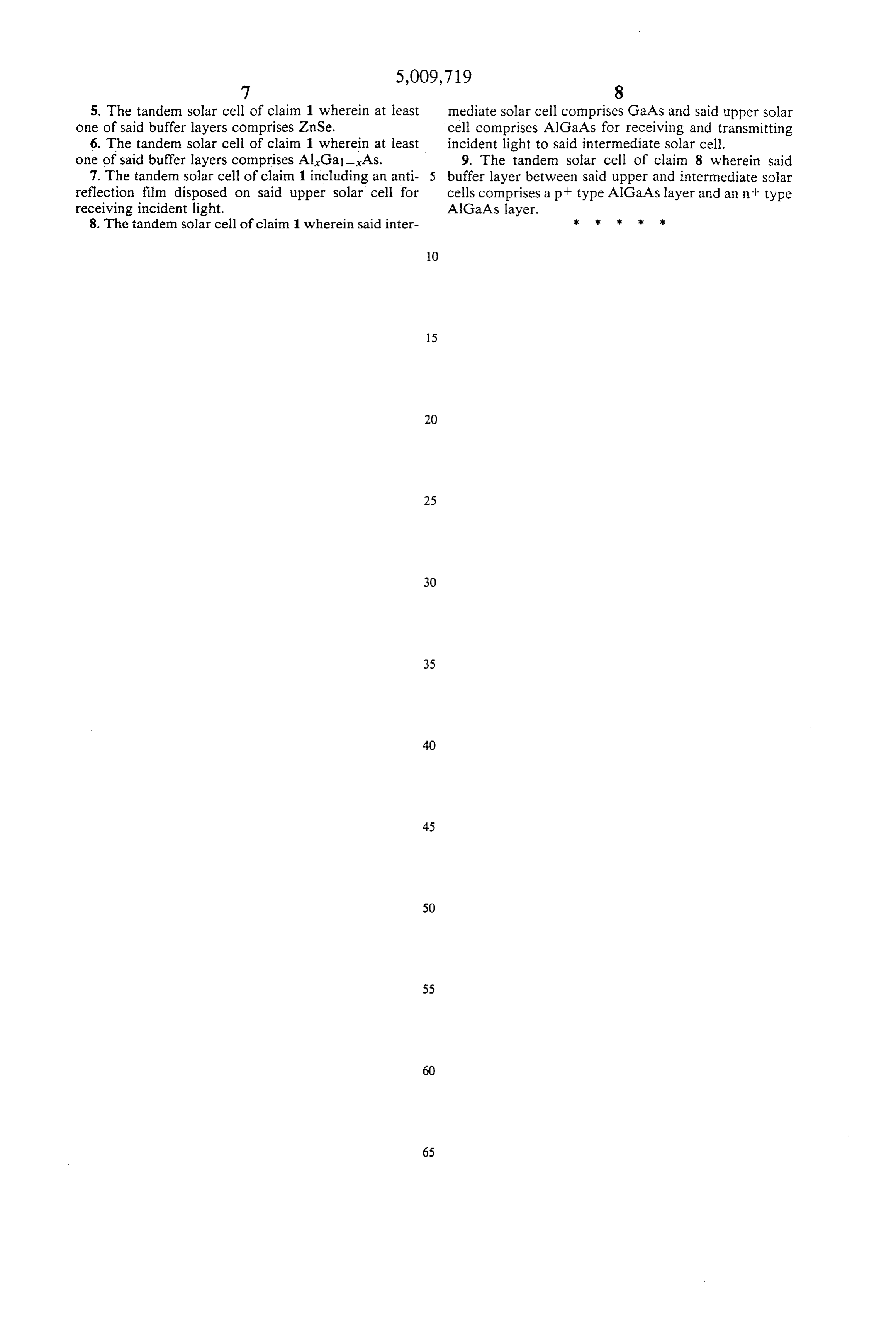
5. The tandem solar cell of claim 1 wherein at least mediate solar cell comprises GaAs and said upper solar one of said buffer layers comprises ZnSe. cell comprises AlGaAs for receiving and transmitting 6. The tandem solar cell of claim 1 wherein at least incident light to said intermediate solar cell. one of said buffer layers comprises AlxGa1-xAs. 9. The tandem solar cell of claim 8 wherein said 7. The tandem solar cell of claim 1 including an anti buffer layer between said upper and intermediate solar reflection film disposed on said upper solar cell for cells comprises apt type AlGaAs layer and an n+ type receiving incident light. AlGaAs layer.
8. The tandem solar cell of claim 1 wherein said inter c xx six :
Provenance
- Collection
- Cited prior art
- Original PDF
- patentimages.storage.googleapis.com →
- Filed
- 1989-11-08
- Pages
- 9
- Method
- pdftotext (the PDF's own text layer) + pdftoppm 300dpi page scans
- Source
- Google Patents bibliographic record
- Granted
- 1991-04-23
- Inventors
- Susumu Yoshida; Mitsubishi Electric Corp
- Transcribed from
- patentimages.storage.googleapis.com →