patent · US4776893
GaAs on GaSb mechanically stacked photovoltaic cells, package assembly, and modules
11 October 1988
Page 1 — bibliographic record
United States Patent (19) 11 Patent Number: 4,776,893 McLeod et al. 45) Date of Patent: Oct. 11, 1988 54 GAASONGASBMECHANICALLY STACKED L. M. Fraas et al., "III-V Cell Research at Chevron,' PHOTOVOLTAIC CELLS, PACKAGE after Jun. 4, 1985. w
ASSEMBLY, AND MODULES L. D. Partain et al., "Vacuum MOVCD Fabrication of 75 Inventors: Paul S. McLeod, Berkeley; John A. High Efficiency Cells for Multijunction Applications' Cape, San Rafael, both of Calif; Apr. 30-May 2, 1985.
Lewis M. Fraas, Isaquah, Wash.; L. M. Fraas et al., "Epitaxial Growth from Organome Larry D. Partain, San Mateo, Calif. tallic Sources in High Vacuum', after Jun 19, 1985. L. D. Partain et al., "High Efficiency Mechanical Stack 73 Assignee: Chevron Research Company, San using A GaAsP Cell on a Transparent Gap Wafer,' Francisco, Calif. Proceedings 18th IEEE Photovoltaic Specialists Con 21 Appl. No.: 921,566 ference Oct. 21-25, 1985, pp. 539-545. 22 Filed: Oct. 21, 1986 Primary Examiner-Aaron Weisstuch Attorney, Agent, or Firm-S. R. LaPaglia; E.J. Keeling;
E. A. Schaal
Related U.S. Application Data
63 Continuation-in-part of Ser. No. 740,362, Jun. 3, 1985,
Pat. No. 4,658,086. The present invention is an apparatus of mechanically 51 Int. Cl. ...................... H01L 31/06; HO1L 25/08 stacked photovoltaic cells having two cells. The bottom 52 U.S.C. ..................................... 136/249; 136/244 cell has a layer of GaSb having regions of different conductivity forming a homojunction therein. The 58 Field of Search ........................... 136/244, 249 TJ GaSb layer is sandwiched between a conductive sub (56) References Cited strate and a bottom passivating layer. In the bottom cell
strate and the incident surface of the bottom passivating 2,949,498 8/1960 Jackson ............................... 136/244 layer. The top cell has a layer of GaAs having regions 4,658,086 4/1987 McLeod et al. .............. 136/249 TJ of different conductivity forming a homojunction OTHER PUBLICATIONS therein, a top passivating layer contacting the surface of the layer of GaAs which is incident to solar radiation,
J. A. Hutchby et al., Cont. Record 18th IEEE Photorol and a means for forming electrical contacts to the layer taic Specialists Conf. (Oct. 1985), pp. 20-27 (Published of GaAs opposed to solar radiation and the incident Apr. 1986). surface of the passivating layer. C. Verié, Conf. Record, 18th IEEE Photoroltaic Special ists Conf. (Oct. 1985, pp. 528-532 (Published Apr. 1986). 13 Claims, 4 Drawing Sheets
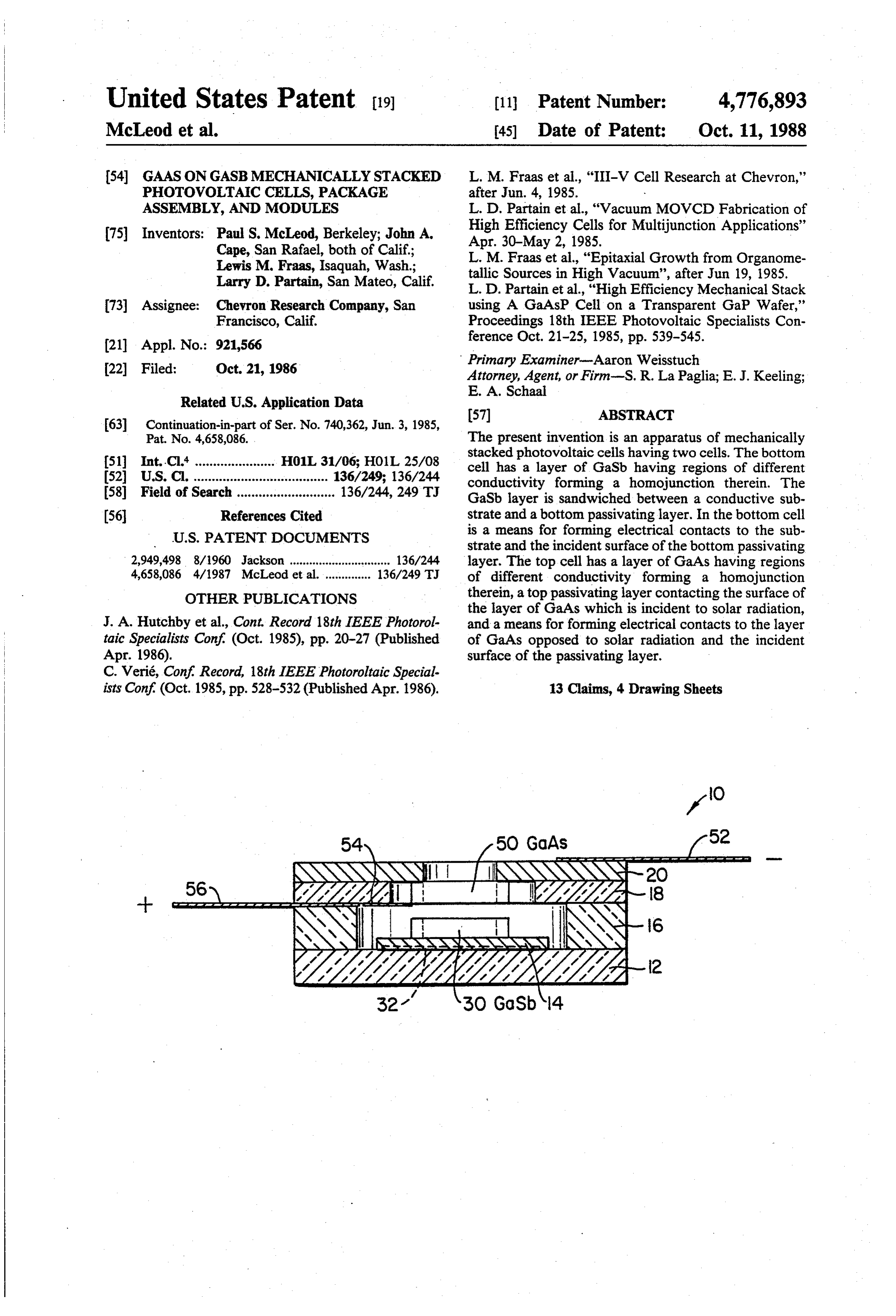
54 5O GOAS 52
NNT IN 2O 56 x HSex 8
- S.sts N 2
Page 2
Drawing sheet — no readable text.
Page 3
Drawing sheet — no readable text.
Page 4
Drawing sheet — no readable text.
Page 5
Drawing sheet — no readable text.
Page 6
connect two photovoltaic cells while minimizing the
GAAS ON GASB MECHANCALLY STACKED effects of heat generated by the concentrated solar radi PHOTOVOLTAIC CELLS, PACKAGE ASSEMBLY, ation.
AND MODULES In conventional mechanical stack designs, in particu lar, those using thin top cells, the heat generated in the
CROSS-REFERENCES TO RELATED top cell must be transmitted through the transparent APPLICATIONS adhesive bonding the two cells together. This can lead This application is a continuation-in-part of our appli to undesirably high cell temperatures. To avoid this cation entitled "Photovoltaic Cell Package Assembly difficulty, it would be highly desirable to have a pack for Mechanically Stacked Photovoltaic Cells', filed on O age design wherein heat spreaders incorporated therein June 3, 1985 and assigned U.S. Ser. No. 740,362 which are used both for the bottom and top cells. A further issued as U.S. Pat. No. 4,658,086. Said application is advantage would be to incorporate a wafer for the top completely incorporated herein by reference for all cell that is thick enough to conduct the heat laterally to purposes. the top heat spreader. A still further advantage would This invention relates to photovoltaic cells. More 15 be to have a design which isolates the cells so that the specifically, this invention relates to mechanically effects of thermal expansion are reduced or minimized. stacked photovoltaic cells. In monolithic cell designs, the top and bottom cells BACKGROUND OF THE INVENTION must generally be current matched or the performance of the cell is limited by the cell having the lower cur
To increase the overall efficiency of photovoltaic 20 rent. Since current matching different bandgap photo cells and extract the maximum amount of energy from voltaic cells can sometimes be difficult, it would be solar radiation, researchers have investigated various desirable to have a package which permits voltage multi-color photovoltaic cells. These multi-color photo matching of the two cells. Voltage matching is benefi voltaic cells can be divided into two general categories. cial because the voltages of the cells change very little The first category covers monolithic multi-color photo 25 with variations in solar spectrum or with the cell degra voltaic cells. A monolithic multi-color photovoltaic cell dation with space radiation damage. Thus, it would also is a photovoltaic cell which has distinct regions opti mized to absorb different portions of the solar radiation be highly desirable to have a package design which can dissipate the heat and permit the easy wiring of numer spectrum in a single cell. U.S. Pat. Nos. 4,404,421 and ous mechanically stacked cells into a module wiring 4,451,691, incorporated herein by reference for all pur 30 configuration poses, describe suitable monolithic cells. Although matching. for voltage matching instead of current these monolithic cells are attractive from a system and Furthermore, it would be desirable to specify two manufacturing point of view, they will require consid component photovoltaic cell materials which will gen erable materials research to bring them to commercial erate voltages which are simple multiples of each other
A second approach involves tandem mechanically where one of these photovoltaic cells is a well devel stacked two-color photovoltaic cells. These cells com oped cell and the other can be rapidly developed to prise independent photovoltaic cells which are opti reach near its theoretical limit performance. Materials mized to the different portions of the solar spectrum and which can be rapidly developed are simple binary com are mechanically and electrically interconnected. These pounds with large optical absorption coefficients which tandem mechanically stacked two-color photovoltaic have already been used as photodetectors. cells offer a shorter path to commercialization primarily SUMMARY OF THE INVENTION because one of the cells can be an already developed cell, such as Si or GaAs. U.S. application Ser. No. The present invention is an apparatus of mechanically 645,456 filed Aug. 28, 1984, incorporated herein by 45 stacked photovoltaic cells having two cells: a bottom reference for all purposes, describes a suitable high GaSb cell and a top GaAs cell. GaAs cells are already band gap photovoltaic cell. Examples of high-band gap well developed and GaSb has been used as a material in photovoltaic cells are GaAsP or AlGaAs or GaAspho photodiodes. The voltage of a GaAs cell will be three tovoltaic cells, and the like. times that of a GaSb cell.
These mechanically stacked cells often fall into the SO The bottom GaSb cell has a layer of GaSb having category of photovoltaic cells known as concentrator regions of different conductivity forming a homojunc photovoltaic cells. A concentrator photovoltaic cell is a tion therein. One surface of the GaSb layer contacts a high efficiency photovoltaic cell which utilizes some conductive substrate, and the opposite surface of the sort of focusing optics to concentrate solar radiation GaSb layer contacts a passivating layer. Preferably, the from a strength of one sun to many suns, i.e., on the 55 passivating layer is a layer of AlyGa(1-Sb, more prefer order of 50 to 1000 or more suns. The concentration of ably, Alo.85Gao.15Sb. Also contained in this cell is a the solar radiation permits the photovoltaic cells to means for forming electrical contacts to the substrate produce a greater amount of electricity per unit area and the incident surface of the passivating layer. than lower efficiency flat plate photovoltaic cells. This The top GaAs cell has a layer of GaAs having re makes them especially useful for space applications 60 gions of different conductivity forming a homojunction where weight is of great concern and in jobs which therein, a passivating layer contacting the surfaces of require maximum electrical output with a minimum the layer of GaAs which is incident to solar radiation, amount of surface area. However, a drawback to con and a means for forming electrical contacts to the layer centrator photovoltaic cells is a means for interconnect of GaAs opposed to solar radiation and the incident ing the two mechanically stacked photovoltaic cells and 65 surface of the passivating layer. Preferably, the passiv dissipating the heat generated by the concentration of ating layer is a layer of AlxGa(1-xAs, more preferably, . the solar radiation. Thus, it would be highly desirable to Alo.85Gao, 15As. The means for forming electrical have mechanically stacked apparatus which can inter contacts in the GaSb cell and the means for forming
Page 7
electrical contacts in the GaAs cell are aligned to pre and the incident surface of the top passivating layer. vent excessive shadowing of the GaSb cell. That means is two sets of metal grids. In one embodiment, six GaSb cells are wired in series The formation of GaAs photovoltaic cells is well for every two GaAs cells wired in series to form a known in the art. One preferred method of forming a module of predetermined output voltage under illumi GaAs cell is disclosed in the paper entitle "Epitaxial nation. In another embodiment, three GaSb cells are Growth from Organometallic Sources in High Vac wired in series for every GaAs cell wired in series to uum' presented by L. M. Fraas, P. S. McLeod, L. D. form a module of predetermined output voltage under Partain, and J. A. Cape at the Electronic Materials illumination. Conference in Boulder, Colo. on June 19, 1975. Said The mechanically stacked apparatus includes top and O paper is incorporated herein by reference for all pur bottom heat spreaders, insulating means to separate the poses.
two photovoltaic cells, and means for forming electrical The bottom GaSb cell comprises a conductive sub contacts to the exposed surfaces of each of the cells strate, a layer of GaSb having regions of different con incorporated into the assembly. The means for forming ductivity forming a homojunction therein and contact electrical contact permit the easy interconnection of the 15 ing the conductive substrate, a passivating layer con completed device in a voltage matching scheme to tacting the surface of the layer of GaSb opposite to the avoid the requirements of current matching the individ surface of the GaSb layer contacting the substrate, and ual cells. means for forming electrical contacts to the substrate BRIEF DESCRIPTION OF THE DRAWINGS and the incident surface of the passivating layer. The conductive substrate can be any material that
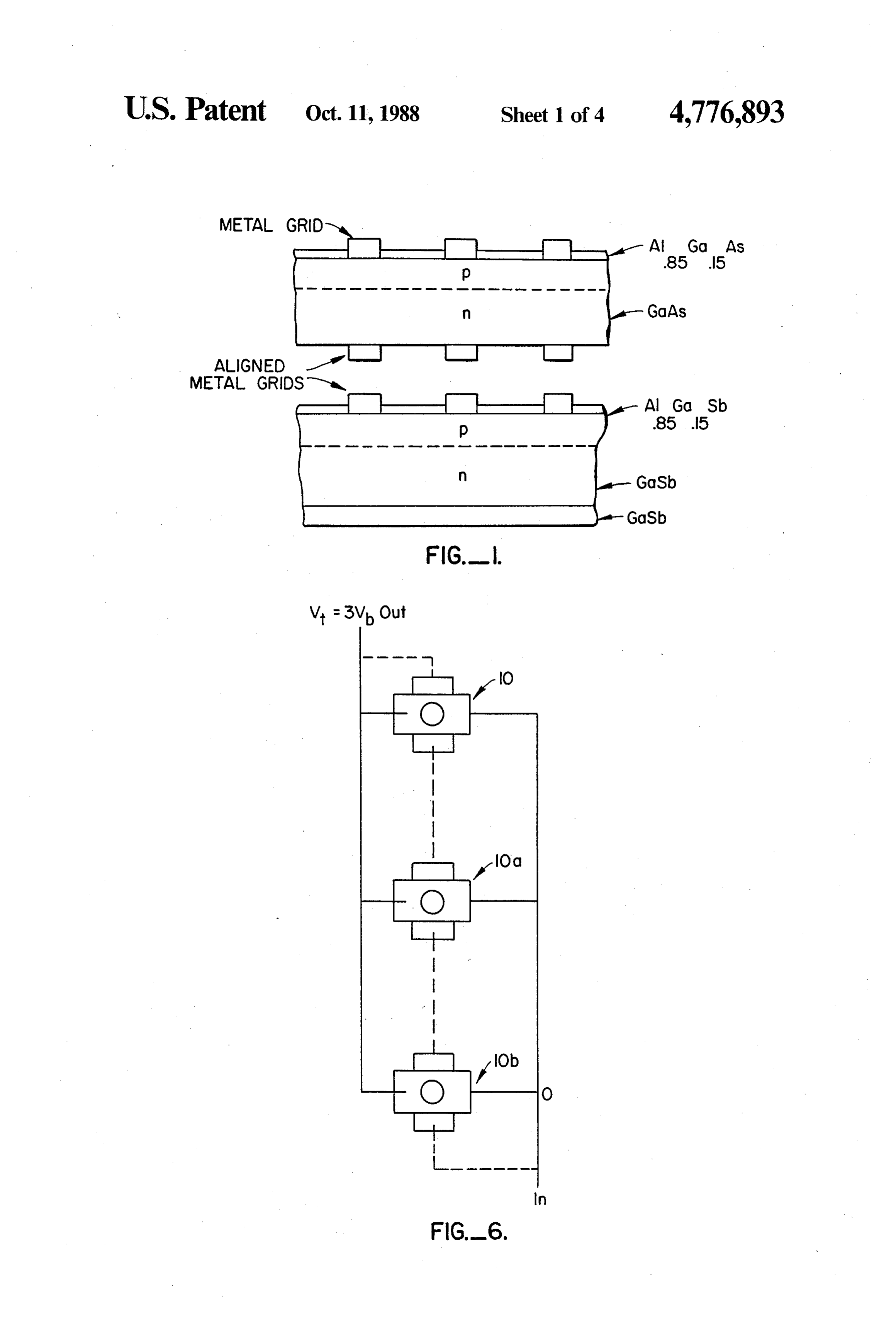
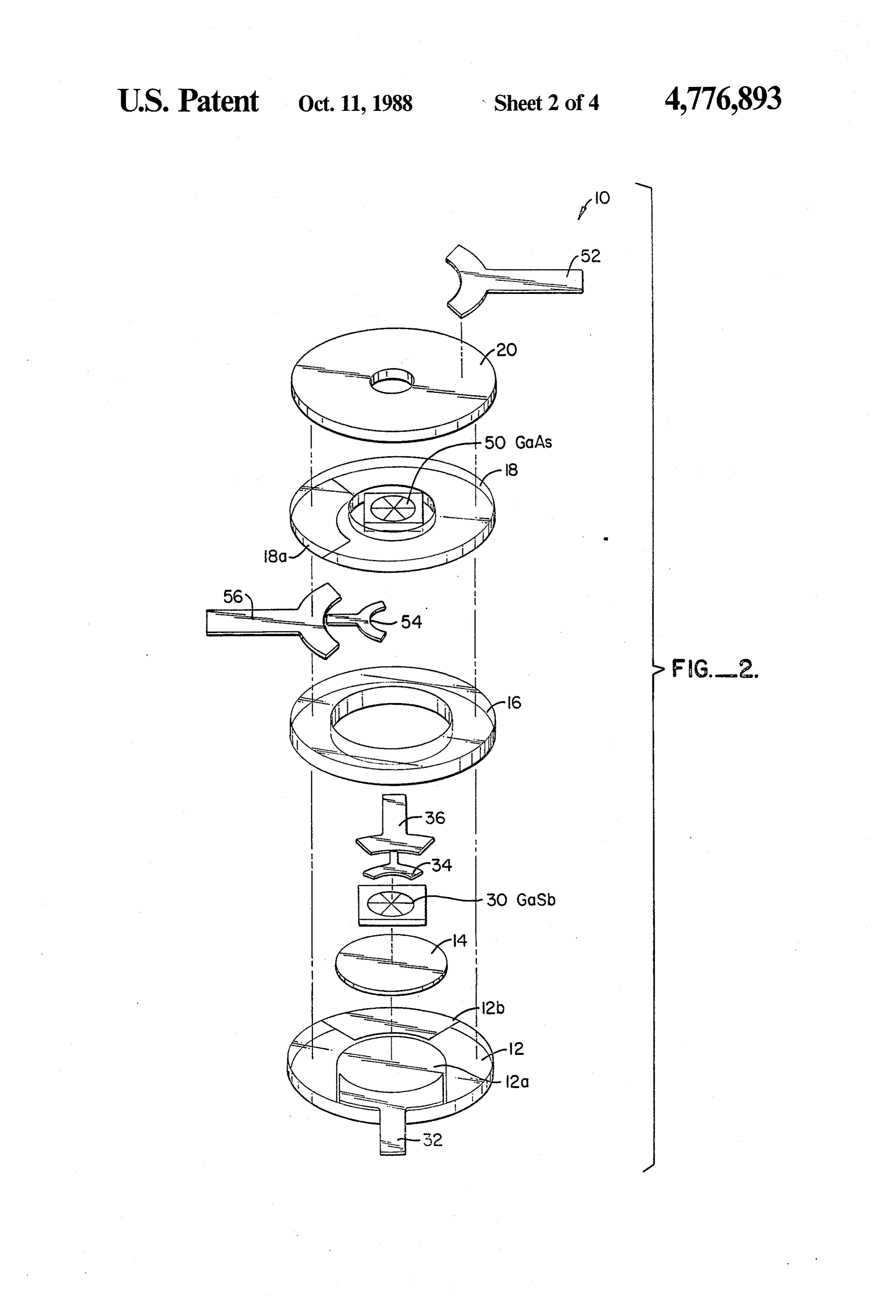
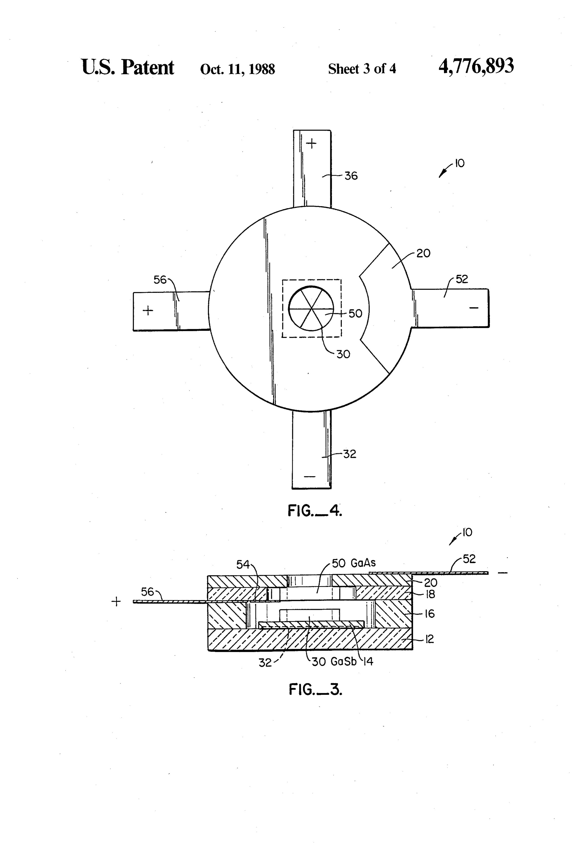
In order to facilitate the understanding of this inven enables the subsequently deposited semiconductor lay tion, reference will now be made to the appended draw ers to grow in a crystal configuration suitable for photo ings of preferred embodiments of the present invention. voltaic cells. A suitable example is crystalline GaSb. The drawings are exemplary only, and should not be As shown in FIG. 1, the layer of GaSb has regions of construed as limiting the invention. 25 different conductivity forming a homojunction therein. FIG. 1 illustrates a side view of one embodiment of Below the homojunction is an n-type GaSb layer that the present invention. contacts the conductive substrate. Above the homo FIG. 2 illustrates an exploded view of the photovol junction, the GaSb layer is doped with a p-type dopant. taic cell package assembly for mechanically stacked A top passivating layer of AlyGa(1-)Sb contacts the photovoltaic cells of our invention. 30 surface of the GaSb layer which is incident to solar FIG. 3 illustrates a cross sectional view of the assem radiation. In FIG. 1, y is equal to 0.85. That figure also bly. shows a means for forming electrical contacts to the FIG. 4 illustrates a top view of the assembly. layer of GaSb opposed to solar radiation and the inci FIG. 5 illustrates a voltage matching module wiring dent surface of the top passivating layer. diagram incorporating twelve mechanically stacked 35 One would expect a GaSb cell fabrication technology photovoltaic assemblies. to closely parallel the GaAs cell fabrication technology FIG. 6 illustrates a voltage matching module wiring in that AlGaSb window layers might be used to passiv diagram incorporating three mechanically stacked pho ate the top surface of a GaSb cell. In fact, F. Capasso et tovoltaic assemblies. al. (Appl. Phys. Letti, 35, 165 (1980)) have used liquid DETAILED DESCRIPTION OF THE phase epitaxy to grow p-type AlGaSb window-pass INVENTION ivated p-on-n GaSb photodiodes; and they have re ported both the current versus voltage and spectral
In its broadest aspect, the present invention is an response characteristics for these devices. apparatus of mechanically stacked photovoltaic cells The means for forming electrical contacts in the having two cells: a bottom GaSb cell and a top GaAs 45 GaSb cell and the means for forming electrical contacts cell. in the GaAs cell are aligned to prevent excessive shad The invention will be more clearly illustrated by owing of the GaSb cell.
referring to the figures. FIG. 1 illustrates a side view of FIGS. 2, 3, and 4 illustrate an exploded view, a cross one embodiment of a mechanically stacked photovol sectional view and a top view, respectively, of a me taic cell package. A top GaAs cell is stacked on a bot 50 chanically stacked photovoltaic cell package 10. The tom GaSb cell. package 10 includes a base support member 12 of a The top GaAs cell comprises a layer of GaAs having suitable insulating material such as alumina (Al2O3) The regions of different conductivity forming a homojunc base support member 12 contains regions of metalliza tion therein, a top passivating layer contacting the sur tion 12a and 12b. These regions provide a means for face of the GaAs layer which is incident to solar radia 55 forming electrical contact to the bottom GaSb cell 30 tion, and means for forming electrical contacts to the through the bottom heat spreader-electrical contact 14 GaAs layer opposed to solar radiation and the incident and the electrode leads 32, 34, and 36. The metallization surface of the top passivating layer. regions 12a and 12b can have any shape which permits As shown in FIG. 1, the layer of GaAs has regions of the formation of electrical contact thereto, although the different conductivity forming a homojunction therein. 60 illustrated configuration is preferred for the contacts On the side of the homojunction incident to solar radia and heat spreaders illustrated. A suitable metallization is tion, the GaAs layer is doped with a p-type dopant. On gold, silver, nickel plating, and the like. The insulating the opposing side, the GaAs layer is doped with an base support member aan be soldered to a suitable heat n-type dopant. A top passivating layer of AlGa(1)As sink, not illustrated, such as a nickel-plated heat sink. contacts the surface of the GaAs layer which is incident 65 Contacting the base support member 12 through the to solar radiation. In FIG. 1, x is equal to 0.85. That metallization 12a is an electrically conductive bottom figure also shows a means for forming electrical heat spreader-electrical contact 14. A suitable bottom contacts to the layer of GaAs opposed to solar radiation heat spreader-electrical contact is fabricated from a
Page 8
suitable thermal expansion matching conductor such as contacts have preferably been illustrated having a Y molybdenum. The bottom heat spreader-electrical shaped configuration, however any suitable configura contact 14 also functions as part of the means for form tion for contacting the appropriate tops and bottoms of ing an electrical contact to the major surface of the cell the cells is possible such as a rectangular a square tab which is opposed to solar radiation. Surrounding this 5 shape. Furthermore, their thicknesses can be adjusted to bottom heat spreader-electrical contact 14 is a bottom provide a more compact or robust assembly as required insulating spacer 16. Preferably the bottom insulating for a particular application.
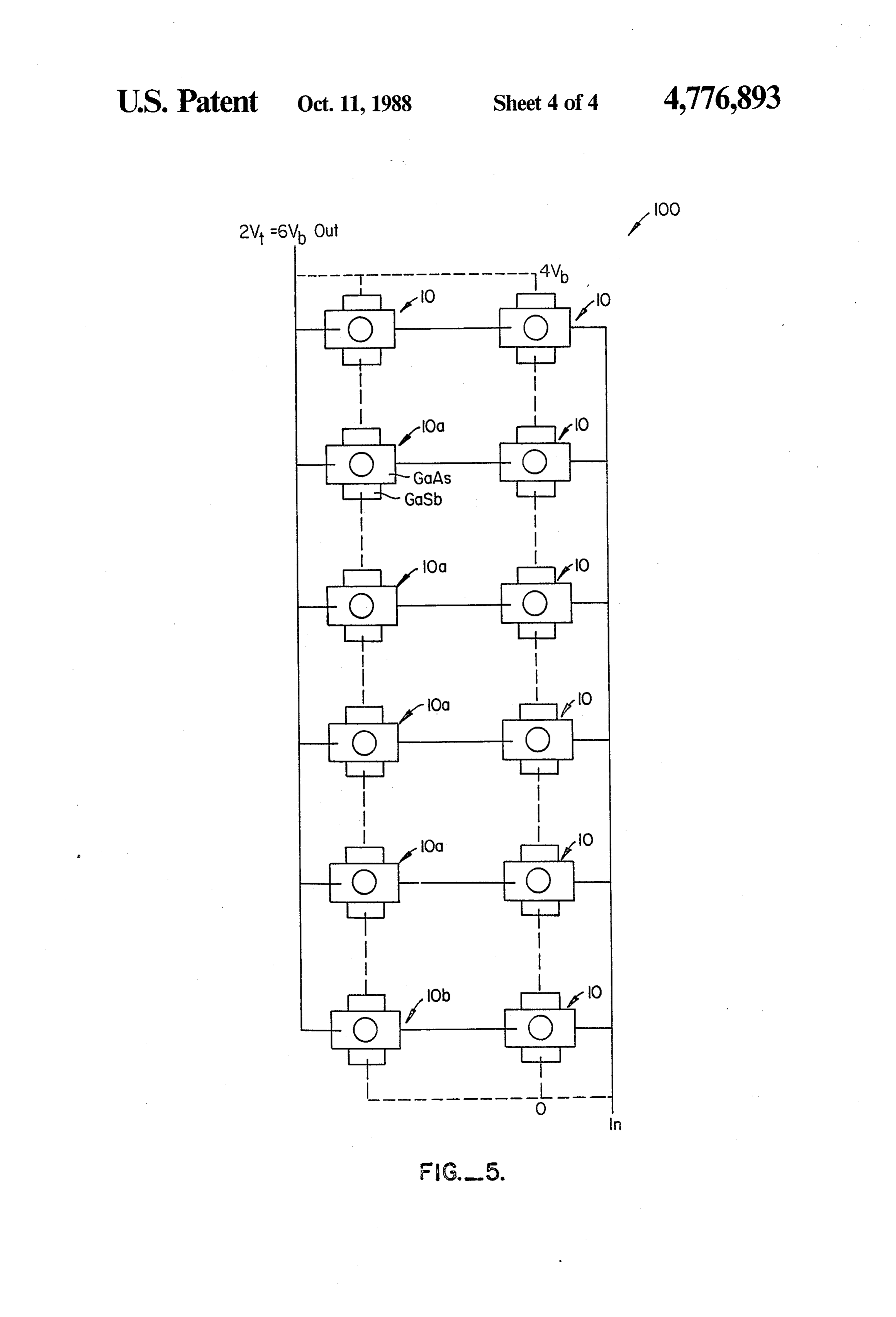
spacer 16 is fabricated from an insulating material such A benefit of the package design 10 permits module as alumina or high temperature plastic and provides a wiring configurations illustrated in FIG. 5. The package space therein surrounding the bottom heat spreader O design 10 avoids the requirement for current matching electrical contact 14 in which to position bottom GaSb of the top and bottom cells and replaces it with a volt cell 30. The bottom GaSb cell 30 is in electrical contact age matching configuration. This wiring scheme bene with the bottom heat spreader-electrical contact 14 and fits from the advantage that the voltage changes very an electrode lead 32 for wiring into a module. little with variations in the solar spectrum or device The bottom GaSb cell 30 is electrically contacted 15 degradation.
with suitable means for forming an electrical contact to cell package Itwhich requires four independent leads from the the portion of the cell opposite to the incident surface. sign described above.is consistent with the package de This combination comprises the bottom heat spreader electrical contact 14, metallization 12a and an electrode forMore specifically, if the stacked cells were designed series connection with currents matched at the be lead 32. The incident surface of the cell is electrically ginning of life, the currents would be mismatched at the
wired into a module through electrode leads 34 and 36. end of life with performance loss greater than the effi Electrode lead 34 electrically contacts the incident ciency loss of the individual cells. Voltage matching surface of bottom GaSb cell 30 and the electrode lead 36 through the metallization 12b. This preferred config provides vary only a longer life design since the device voltages logarithmically with current changes. FIG. 5 uration permits the bottom GaSb cell 30 to be isolated 25 from the rest of the package 10 and thus minimizes the illustrates a six by two module wiring diagram for volt thermal expansion strains placed upon the bottom GaSb age matching of top and bottom cells whose output cell 30 during the heating thereof caused by solar radia voltages differ by a factor of 3. For the twelve element tion. Although less preferred, the electrode leads 34 and configuration illustrated, six of the bottom and two of 36 can be configured if desired as a unitary piece. Of 30 the top cells are connected in series to provide voltage course, if electrode leads 34 and 36 were a single piece matching. Different voltage ratios for different photo of metal then the metallization 12b would be unneces voltaic cells would require other series and parallel sary. The preferred configuration of the top and bottom connection schemes for voltage matching, e.g., four by leads to the bottom GaSb cell 30 is illustrated. Of three, seven by five, five by three, etc. The only limita course, depending upon the packaging the electrode 35 tions on the interconnection schemes are the voltages of leads 32, 34, and 36 need not be opposed but could be the different cells. Of course, different modules having fabricated over but separated from each other. A fur specific output currents and voltages can be connected ther option, not illustrated, would be to have the metal in series or parallel to provide any desired overall volt lization illustrated as 12b on base support member 12 age or current output for a particular application. applied instead on the bottom insulating spacer 16. This 40 FIG. 6 illustrates a three by one module wiring dia option would avoid the tab portion of electrode lead 34 gram for voltage matching of top and bottom cells from having to bend down from the incident surface of whose output voltages differ by a factor of 3. For the bottom GaSb cell 30 to the metallization 12b on base three element configuration illustrated, three of the support member 12.
A top insulating spacer 18 such as alumina, a high 45 bottom and one of the top cells are connected in series to provide voltage matching.
temperature plastic, and the like, separates the bottom While the present invention has been described with GaSb cell 30 from the top GaAs cell 50. The top GaAs reference cell 50 is electrically contacted on the bottom, i.e., the intended totocover specific embodiments, this application is major surface opposite the incident surface through tions which may bethose various changes and substitu made by those skilled in the art electrode leads 54 and 56 and the metallization 18a on 50 the top insulating spacer 18. These bottom leads can without departing from the spirit and scope of the ap also be configured as a single unitary piece. The inci to the ordinary Modifications pended claims.
skilled artisan, which would be obvious such as selection of par dent surface of the photovoltaic cell is in electrical ticular top and bottom photovoltaic cells and configura contact with a top heat spreader-electrical contact 20 tion of the spreaders and insulators are for spreading the heat from the top GaAs cell 50 and the be within the scope of the invention. contemplated to
electrode lead 52. A suitable top heat spreader-electrical What is claimed is:
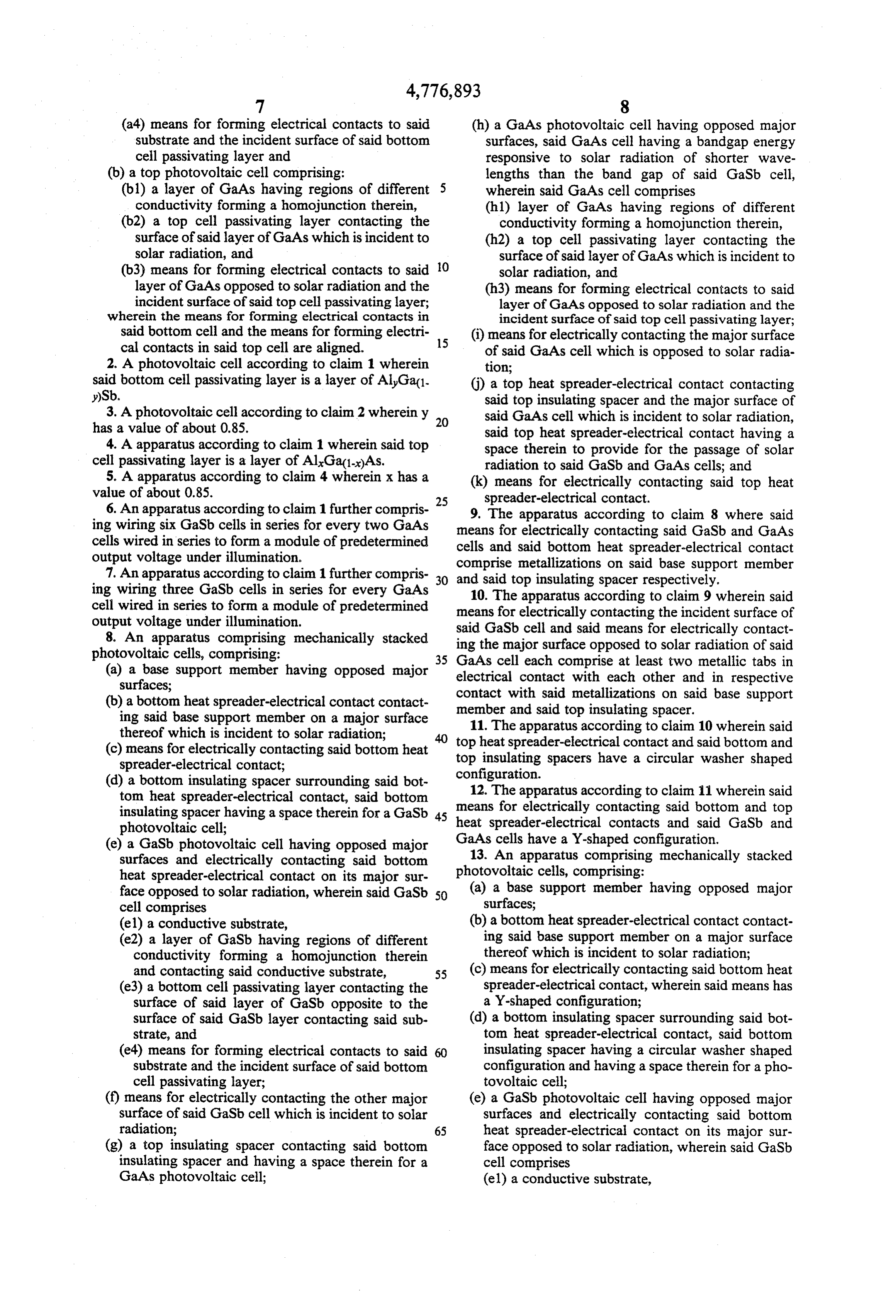
contact 20 is a molybdenum heat sink in contact with top GaAs cell 50. The electrode lead 52 can be any 1. An apparatus comprising mechanically stacked suitable metal. Of course, the top heat spreader-electri photovoltaic cells, comprising: cal contact 20 has a hole therein, as illustrated, for the (a) a bottom photovoltaic cell comprising: passage of solar radiation. (a1) a conductive substrate, Although the package assembly 10 has been de (a2) a layer of GaSb having regions of different scribed and illustrated with spacers and heat spreaders conductivity forming a homojunction therein having a circular washer shaped configuration, any and contacting said conductive substrate, suitable configuration for the spacers and heat spreaders 65 (a3) a bottom cell passivating layer contacting the is possible provided they contain a space therethrough surface of said layer of GaSb opposite to the for which the solar radiation to enter into the top GaAs surface of said GaSb layer contacting said sub cell 50 and pass to the bottom GaSb cell 30. The strate, and
Page 9
(a4) means for forming electrical contacts to said (h) a GaAs photovoltaic cell having opposed major substrate and the incident surface of said bottom surfaces, said GaAs cell having a bandgap energy cell passivating layer and responsive to solar radiation of shorter wave (b) a top photovoltaic cell comprising: lengths than the band gap of said GaSb cell, (b1) a layer of GaAs having regions of different wherein said GaAs cell comprises conductivity forming a homojunction therein, (h1) layer of GaAs having regions of different (b2) a top cell passivating layer contacting the conductivity forming a homojunction therein, surface of said layer of GaAs which is incident to (h2) a top cell passivating layer contacting the solar radiation, and surface of said layer of GaAs which is incident to (b3) means for forming electrical contacts to said O solar radiation, and layer of GaAs opposed to solar radiation and the (h3) means for forming electrical contacts to said incident surface of said top cell passivating layer; layer of GaAs opposed to solar radiation and the wherein the means for forming electrical contacts in incident surface of said top cell passivating layer; said bottom cell and the means for forming electri 15 (i) means for electrically contacting the major surface cal contacts in said top cell are aligned. of said GaAs cell which is opposed to solar radia 2. A photovoltaic cell according to claim 1 wherein tion;
said bottom cell passivating layer is a layer of AlyGa(1- (j) a top heat spreader-electrical contact contacting y)Sb. said top insulating spacer and the major surface of 3. A photovoltaic cell according to claim 2 wherein y 20 said GaAs cell which is incident to solar radiation, has a value of about 0.85. said top heat spreader-electrical contact having a 4. A apparatus according to claim 1 wherein said top space therein to provide for the passage of solar cell passivating layer is a layer of AlxGa(1-x)4s. radiation to said GaSb and GaAs cells; and 5. A apparatus according to claim 4 wherein x has a (k) means for electrically contacting said top heat value of about 0.85. 25 spreader-electrical contact. 6. An apparatus according to claim 1 further compris 9. The apparatus according to claim 8 where said ing wiring six GaSb cells in series for every two GaAs means for electrically contacting said GaSb and GaAs cells wired in series to form a module of predetermined cells and said bottom heat spreader-electrical contact output voltage under illumination.
7. An apparatus according to claim 1 further compris 30 comprise metallizations on said base support member and said top insulating spacer respectively.
ing wiring three GaSb cells in series for every GaAs 10. The apparatus according to claim 9 wherein said cell wired in series to form a module of predetermined means for electrically contacting the incident surface of output voltage under illumination. said GaSb cell and said means for electrically contact 8. An apparatus comprising mechanically stacked ing the major surface opposed to solar radiation of said photovoltaic cells, comprising: 35 GaAs cell each comprise at least two metallic tabs in (a) a base support member having opposed major electrical contact with each other and in respective surfaces;
(b) a bottom heat spreader-electrical contact contact contact member with said metallizations on said base support and said top insulating spacer.
ing said base support member on a major surface 11. The apparatus according to claim 10 wherein said thereof which is incident to solar radiation;
(c) means for electrically contacting said bottom heat top insulating spacers havecontact top heat spreader-electrical and said bottom and a circular washer shaped spreader-electrical contact;
(d) a bottom insulating spacer surrounding said bot configuration.
tom heat spreader-electrical contact, said bottom means 12. The apparatus according to claim 11 wherein said insulating spacer having a space therein for a GaSb 45 for electrically contacting said bottom and top photovoltaic cell; heat spreader-electrical contacts and said GaSb and (e) a GaSb photovoltaic cell having opposed major GaAs cells have a Y-shaped configuration. 13. An apparatus comprising mechanically stacked surfaces and electrically contacting said bottom photovoltaic heat spreader-electrical contact on its major sur cells, comprising: face opposed to solar radiation, wherein said GaSb 50 (a) a base support member having opposed major cell comprises surfaces;
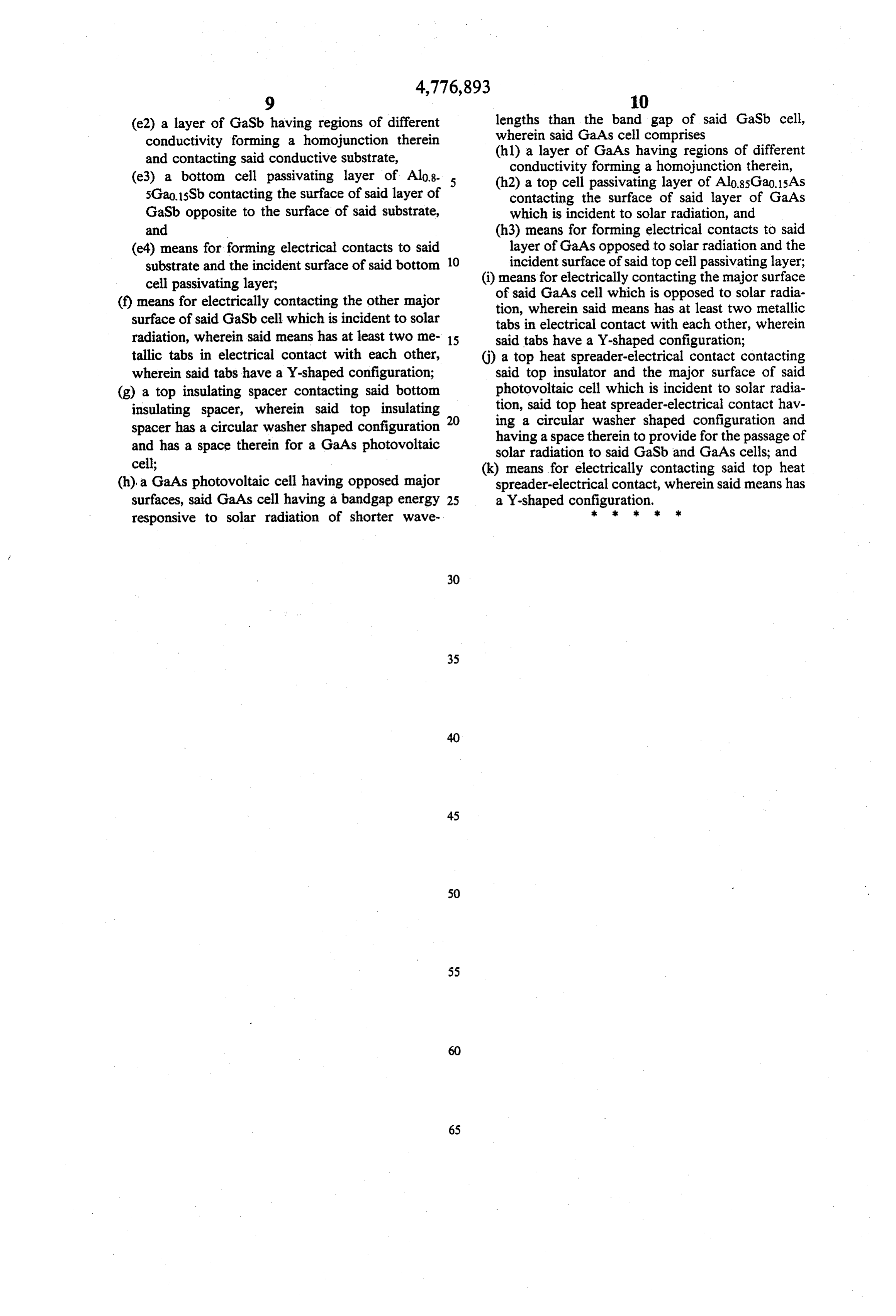
(el) a conductive substrate, (b) a bottom heat spreader-electrical contact contact (e2) a layer of GaSb having regions of different ing said base support member on a major surface conductivity forming a homojunction therein thereof which is incident to solar radiation; and contacting said conductive substrate, 55 (c) means for electrically contacting said bottom heat (e3) a bottom cell passivating layer contacting the spreader-electrical contact, wherein said means has surface of said layer of GaSb opposite to the a Y-shaped configuration;
surface of said GaSb layer contacting said sub (d) a bottom insulating spacer surrounding said bot strate, and tom heat spreader-electrical contact, said bottom (e4) means for forming electrical contacts to said insulating spacer having a circular washer shaped substrate and the incident surface of said bottom configuration and having a space therein for a pho cell passivating layer; tovoltaic cell;
(f) means for electrically contacting the other major (e) a GaSb photovoltaic cell having opposed major surface of said GaSb cell which is incident to solar surfaces and electrically contacting said bottom radiation; 65 heat spreader-electrical contact on its major sur (g) a top insulating spacer contacting said bottom face opposed to solar radiation, wherein said GaSb insulating spacer and having a space therein for a cell comprises
GaAs photovoltaic cell; (el) a conductive substrate,
Page 10
(e2) a layer of GaSb having regions of different lengths than the band gap of said GaSb cell, conductivity forming a homojunction therein wherein said GaAs cell comprises and contacting said conductive substrate, (hl) a layer of GaAs having regions of different conductivity forming a homojunction therein, (e3) a bottom cell passivating layer of Alo.8- 5 (h2) a top cell passivating layer of Alo.85Gao.15As 5Gao.15Sb contacting the surface of said layer of contacting the surface of said layer of GaAs GaSb opposite to the surface of said substrate, which is incident to solar radiation, and and (h3) means for forming electrical contacts to said (e4) means for forming electrical contacts to said layer of GaAs opposed to solar radiation and the substrate and the incident surface of said bottom 10 incident surface of said top cell passivating layer; cell passivating layer; (i) means for electrically contacting the major surface (f) means for electrically contacting the other major of said GaAs cell which is opposed to solar radia surface of said GaSb cell which is incident to solar tion, wherein said means has at least two metallic tabs in electrical contact with each other, wherein radiation, wherein said means has at least two me 15 said tabs have a Y-shaped configuration; tallic tabs in electrical contact with each other, (j) a top heat spreader-electrical contact contacting wherein said tabs have a Y-shaped configuration; said top insulator and the major surface of said (g) a top insulating spacer contacting said bottom photovoltaic cell which is incident to solar radia insulating spacer, wherein said top insulating tion, said top heat spreader-electrical contact hav spacer has a circular washer shaped configuration 20 ing a circular washer shaped configuration and and has a space therein for a GaAs photovoltaic having a space therein to provide for the passage of solar radiation to said GaSb and GaAs cells; and cell; (k) means for electrically contacting said top heat (h) a GaAs photovoltaic cell having opposed major spreader-electrical contact, wherein said means has surfaces, said GaAs cell having a bandgap energy 25 a Y-shaped configuration.
responsive to solar radiation of shorter wave
Page 11
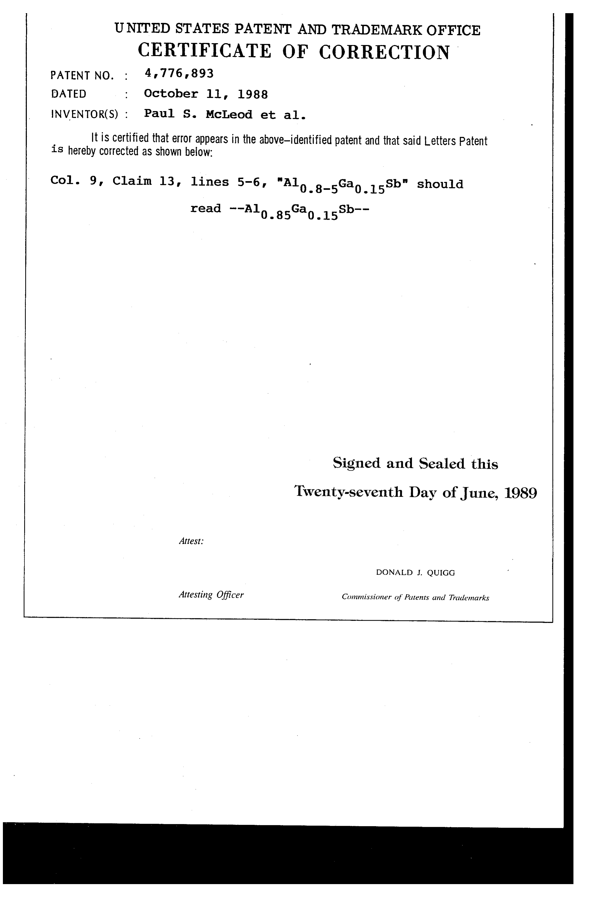
UNITED STATES PATENT AND TRADEMARK OFFICE
CERTIFICATE OF CORRECTION
INVENTOR(S) : Paul S. McLeod et al.
It is certified that error appears in the above-identified patent and that said Letters Patent is hereby corrected as shown below:
Col. 9, Claim l3 lines 5-6, "All 0.8-5Gao.15Sb" should
read Alo. 85Gao.15 Sb--
Signed and Sealed this
Twenty-seventh Day of June, 1989
DONALD J. QUIGG
Attesting Officer Commissioner of Patents and Trademarks
Provenance
- Collection
- Cited prior art
- Original PDF
- patentimages.storage.googleapis.com →
- Filed
- 1986-10-21
- Pages
- 11
- Method
- pdftotext (the PDF's own text layer) + pdftoppm 300dpi page scans
- Source
- Google Patents bibliographic record
- Granted
- 1988-10-11
- Inventors
- Paul S. McLeod; John A. Cape; Lewis M. Fraas; Larry D. Partain; Chevron Research Co
- Transcribed from
- patentimages.storage.googleapis.com →