patent · US4634641
Superlattice photoelectrodes for photoelectrochemical cells
6 January 1987
Page 1 — bibliographic record
United States Patent (19) 11) Patent Number: 4,634,641 Nozik 45) Date of Patent: Jan. 6, 1987 (54) SUPERLATTICE PHOTOELECTRODES FOR Primary Examiner-Aaron Weisstuch PHOTOELECTROCHEMICAL CELLs Attorney, Agent, or Firm-Kenneth L. Richardson; Michael J. Higgins; Judson R. Hightower 75 Inventor: Arthur J. Nozik, Boulder, Colo.
73 Assignee: The United States of America as 57 ABSTRACT represented by the United States A superlattice or multiple-quantum-well semiconductor Department of Energy, Washington,
D.C. is used as a photoelectrode in a photoelectrochemical process for converting solar energy into useful fuels or 21) Appl. No.: 751,413 chemicals. The quantum minibands of the superlattice 22 Filed: Jul. 3, 1985 or multiple-quantum-well semiconductor effectively capture hot-charge carriers at or near their discrete 51 int. Cl'.............................................. H01M 6/36 quantum energies and deliver them to drive a chemical 52 U.S.C. ................................ 429/111; 204/290 R; reaction in an electrolyte. The hot-charge carries can be 204/DIG. 3 injected into the electrolyte at or near the various dis 58) Field of Search ................ 429/111; 204/128, 129, crete multiple energy levels quantum minibands, or 204/242, 248,278, 290 R, DIG. 3 they can be equilibrated among themselves to a hot-car 56) References Cited rier pool and then injected into the electrolyte at one PUBLICATIONS average energy that is higher than the lowest quantum A. J. Nozik et al, Nature, vol. 316, Jul. 4, 1985, pp. band gap in the semiconductor.
M. Archer, Nature, vol. 316, Jul. 4, 1985, pp. 15-16. 20 Claims, 9 Drawing Figures
Page 2
Drawing sheet — no readable text.
Page 3
Drawing sheet — no readable text.
Page 4
Drawing sheet — no readable text.
Page 5
Drawing sheet — no readable text.
Page 6
Drawing sheet — no readable text.
Page 7
trochemical cell to drive chemical oxidation and reduc
SUPERLATTCE PHOTOELECTRODES FOR tion reactions on the surfaces of the semiconductor PHOTOELECTROCHEMICAL CELLS electrode and counter electrode in the cell. See, for example, Robert T. Ross and Arthur J. Nozik, "Effi
CONTRACTUAL ORIGIN OF THE INVENTION ciency of Hot-Carrier Solar Energy Converters', Jour The United States Government has rights in this nal of Applied Physics, vol. 53, pp. 3813-3818 (1982); A. invention under Contract No. DE-AC02-83CH10093 J. Nozik, "Photoelectrochemical Devices for Solar between the U.S. Department of Energy and the Solar Energy Conversion', Photovoltaic and Photoelectro Energy Research Institute, a Division of Midwest Re 10 chemical Solar Energy Conversion, pp. 263-312 (Ple search Institute. num Publishing Corporation, 1981); Arthur J. Nozik, "Introductory. Lecture: Photoelectrochemistry”, Fara
BACKGROUND OF THE INVENTION day Discussions of the Royal Society of Chemistry, No. 70, 1. Field of the Invention Photoelectrochemistry (1980); A. J. Nozik, et al. This invention relates generally to photoelectro 5 "Charge Transfer at Illuminated Semiconductor-Elec chemical energy conversion techniques and, more spe trolyte Interfaces', Interfacial Photoprocesses: Energy cifically, to the application of superlattice semiconduc Conversion and Synthesis, Advances in Chemistry Series tors as photoelectrodes in photoelectrochemical energy vol. 184, American Chemical Society (1980), based on a conversion processes. symposium sponsored by the Division of Colloid and 2. Description of the Prior Art Surface Chemistry at the 176th meeting of the Ameri Photovoltaic cells, commonly known as solar cells, 20 can Chemical Society, Miami Beach, Fla., Sept. 11-13, are essentially semiconductors that have capability of 1978; Arthur J. Nozik, "Photoelectrochemistry: Appli converting electromagnetic energy, such as light or cations to Solar Energy Conversion,” Ann. Rev. Phys. solar radiation, directly to electricity. Such semicon Chem, vol. 29, pp. 189-222 (1978); Gerald Cooper, et al. ductors are usually characterized by solid crystalline "Hot Carrier Injection of Photogenerated Electrons at structures that have energy band gaps between their 25 Indium Phosphide-Electrolyte Interfaces', Journal of valence electron bands and their conduction electron Applied Physics, vol. 54, pp. 6463-6473 (1983); John A. bands. Free electrons normally cannot exist or remain in Turner and Arthur J. Nozik, "Evidence for Hot-Elec these band gaps. However, such photovoltaic cells are tron Injection Across p-Gap/Electrolyte Junctions', also characterized by materials of a type that when light Applied Physics Letters, vol. 41, pp. 101-103 (1982); D.S. is absorbed by them, electrons that occupy low-energy 30 Boudreaux, et al. "Hot Carrier Injection at Semicon states are excited to jump the band gap to unoccupied ductor-Electrolyte Junctions”, Journal of Applied Phys higher-energy states. For example, when electrons in ics, vol. 51, pp. 2158-2163 (1980); F. Williams and A. J. the valence band of a semiconductor absorb sufficient Nozik, "Solid State Perspectives of the Photoelectro energy from photons of the solar radiation, they can chemistry of Semiconductor-Electrolyte Junctions', jump the band gap to the higher-energy conduction Nature, vol. 311, pp. 21-27 (1984); J. A. Turner, et al.
band. "Photoelectrochemistry with p-SElectrodes: Effects of Electrons so excited to higher-energy states leave Inversion”, Applied Physics Letters, vol. 37, pp. 488-491 behind them unoccupied low-energy positions or (1980); J. A. Turner, "SupraBand-Edge Reactions at "holes.' Such "holes' can shift from atom to atom in Semiconductor-Electrolyte Interfaces: Band-Edge Un the crystal lattice; thus, the holes act as charge carriers, pinning Produced by the Effects of Inversion', Ameri as do free electrons, and contribute to the crystal's con can Chemical Society Symposium Series (1980). ductivity. Therefore, most of the photons that are ab Electrolysis is, of course, the decomposition of a sorbed in the semiconductor give rise to such electron chemical hole pairs. It is these electron-hole pairs that generate ple, it is a compound by an electrode current. For exam the photocurrent and, in turn, the photovoltage exhib 45 comprisingcommon process to decompose an electrolyte water, i.e., H2O into its constituent elements ited by solar cells. of hydrogen and oxygen in a redox reaction generally These electron-hole pairs produced by the light described as:
would eventually recombine, thereby converting to heat or a photon the energy initially used to jump the band gap, unless prohibited from doing so. Therefore, a 50 local electric field is created in the semiconductor by where "doping" or interfacing dissimilar materials to produce a space-charge layer. This space-charge layer serves to separate the holes and electrons for use as charge carri ers. Once separated, these collected hole and electron 55 and charge carriers produce a space charge that results in a voltage across the junction, which is the photovoltage.
If these separated hole and charge carriers are allowed to flow through an external load before recombining, In such an electrolysis process, the hydrogen gas (H2) they constitute a photocurrent. bubbles off the negative electrode or cathode, and the The photocurrent generated in a solar cell can be oxygen gas (O2) bubbles off the positive electrode or utilized in a number of ways. It can be collected at solid anode. The hydrogen and oxygen gases can, of course, contacts or electrodes on the semiconductor and di be put to many wellknown beneficial uses, including the rected by conductors through external electrical loads production of fuel.
to perform useful work. Also, much work has been 65 One of the historic impediments to the large-scale use done in the field of utilizing the photocurrent internally of electrolysis processes for the production of fuel has in an electrolysis processes. That is, the separated elec been the inefficiencies of such processes. Specifically, tron-hole pairs are utilized immediately in a photoelec the electric energy input required to drive the redox
Page 8
reaction is not justified by the energy output available normally occurs in about 10-12 seconds, the photocur from the fuel derived in the process. However, interest rent delivered to a load or injected into an electrolyte in this area has been increased by the possible use of comprises carriers having energy levels at the lower solar radiation to drive the redox reaction through the edge of the conduction band. In other words, the effec use of solar cell semiconductors as electrodes in the 5 tive photovoltage of a single band gap semiconductor is electrolysis process. limited by the band gap.
Such processes, now commonly referred to as photo The practical effect of this limitation prior to this electrochemical energy conversion, are the subject of invention was that the semiconductor designer had to the previously-cited references. They essentially com sacrifice efficiencies in one area in order to achieve prise immersing a semiconductor material in a liquid 10 them in another. Specifically, in order to capture as electrolyte and exposing the semiconductor material to many photons from the spectrum of solar radiation as light. The semiconductor-liquid interface creates the possible, the semiconductor had to be designed with a local electric field to produce the depletion zone (or small band gap so that even small photons from lower space charge) and under illumination generates a volt energy radiation could excite electrons to jump the age and current across the semiconductor-liquid inter- 15 band gap. However, in doing so, there were at least two face. Such an interface is essentially like a Schottky negative effects that had to be traded. First, the small semiconductor heterojunction formed by an interface of band gap resulted in a low photovoltage device, thus different materials, although the term Schottky hetero low power output. Second, the more energetic photons junction is usually used to refer to a solid semiconduc from higher energy radiation produced many hot carri tor-metal interface. 20 ers having much excess energy that would be lost as When exposed to light, the internal photocurrent heat upon almost immediate thermalization of these hot induced in the semiconductor drives the electrolysis carriers to the edge of the conduction band. On the reaction. Essentially, the photoexcited charge carriers other hand, if the semiconductor is designed with a (electrons that have jumped the band gap to the higher larger band gap to increase the photovoltage and re energy level conduction band) are injected into the 25 duce energy loss caused by thermalization of hot carri electrolyte from the semiconductor before the electron ers, then the smaller photons from lower-energy radia hole pairs can recombine across the band gap. Such tion will not be absorbed.
charge carriers injected into the electrolyte take part in Consequently, prior to this invention, it was neces : the redox chemical reaction in the electrolysis process. sary to balance these considerations and try to design a It is known, as also discussed in the previously-cited 30 semiconductor with an optimum band gap, realizing references, that photon energies in excess of the thresh that in the balance, there had to be a significant loss of . . sold energy gap or band gap between the valence and energy from both large and small energy photons. It has conduction bands are usually dissipated as heat, and been calculated that the theoretical maximum energy thus are wasted and do no useful work. More specifi conversion with conventional single band gap semicon cally, there is a fixed guantum of potential energy differ- 35 ductors is about 31%. However, if all the photon en ence across the band gap in the semiconductor. In order ergy from the visible light spectrum could be captured ... for an electron in the lower-energy valence band to be and used, the theoretical conversion efficiency of a '...excited to jump the band gap to the higher-energy con semiconductor would be about 68%. ...duction band, it has to absorb a sufficient quantum of Many of the previously-cited references are directed genergy, usually from an absorbed photon, with a value 40 at attempts to increase conversion efficiency by captur at least equal to the potential energy difference across ing and utilizing the excess energy of hot carriers by the band gap. injecting them into an electrolyte for driving redox If the electron absorbs less than that required for the reactions before they thermalize. The theory of such threshold quantum of energy, it will not be able to make attempts is that if the thermalization time of hot carriers the jump across the band gap. Such energy is essentially 45 was greater than their residence time in the semicon lost for practical purposes. ductor, then hot-carrier injection into the electrolyte On the other hand, if the electron absorbs more than could occur. However, because of the extremely rapid the threshold quantum of energy, e.g., from a larger thermalization of the hot carriers, which occurs in energy photon, it can jump the band gap. The excess of about a picosecond in bulk semiconductors, no one has such absorbed energy over the threshold quantum re- 50 been able to achieve this goal prior to this invention. quired for the electron to jump the band gap results in It had been throught prior to this invention that it was the electron being higher in energy than most of the necessary to either slow down the thermalization rate other electrons in the conduction band. Such electrons significantly or to find a way to remove the hot carriers having energy levels higher than the lower edge of the in less than a picosecond. For example, in the previous conduction band, i.e., the top edge of the band gap, are 55 ly-cited reference, Robert T. Ross and Arthur J. Nozik, referred to as "hot electrons'. For every electron ex “Efficiency of Hot-Carrier Solar. Energy Converters', cited out of its normal energy level, there is a corre Journal of Applied Physics, vol.53, pp. 3813-3818 (1982), sponding "hole'. Thus, for each hot electron, there can it was suggested that with highly doped semiconductors be a corresponding hot hole, both of which are gener used in combination with semiconductor-liquid or semi ally referred to as "hot carriers'. 60 conductor-solid interfaces where large electric fields Hot carriers usually lose their excess energy to the exist because of initial chemical potential differences host lattice very rapidly in the form of heat. This pro between the phases, resulting quantization effects in the cess, in which the hot carriers dissipate their excess space charge layer would slow down the thermalization energy to the host lattice and equilibrate with the lattice process and enhance hot carrier charge transfer out of at ambient temperature, is known as thermalization. 65 the semiconductor. However, nothing close to the ulti Such thermalization of hot carriers results in the carri mate theoretical conversion efficiencies of 66% could ers being reduced in energy to the energy level at the be attaind by such systems because most of the thermali edge of the conduction band. Since such thermalization zation of photogenerated hot carriers occurs in the
Page 9
much larger bulk region of the semiconductor (where charge carriers in the conduction bands of the well the energy bands are flat) rather than in the small deple layer.
tion zone or space-charged region where the band It is known that the potential or quantum wells split bending and quantization effects occur. the valence bands and the conduction bands into a plu Consequently, there remains a need for a device that rality of minibands. These minibands are narrower than can capture and utilize a large range of photon energies the bands in a bulk semiconductor and are separated from the solar radiation spectrum, yet not sacrifice from each other in the conduction band by relatively either photovoltage or excess energy loss to heat by large minigaps. A result of this structure is that elec thermalization of hot carriers. This need has remained tron-hole pairs can be held separated for longer periods unsatisfied until this invention. 10 before they recombine. Also, photons are absorbed only Another development that was occuring about the if their energies equal or exceed a threshold value deter same period as the attempts just described to utilize mined not by the band gap of either semiconductor photoelectrochemical processes for solar energy con alone, but by the effective band gap, which is the differ version, although in different research endeavors, was ence in energy between the least energetic conduction the development of superlattice semiconductor struc 15 miniband and the most energetic valence miniband. tures. Much of the development, experimentation, ob Further, photon absorption is maximized where photon servations, and theories of such superlattice semicon energies correspond to the differences in energy be ductor structures are reported or described in the fol tween pairs of minibands.
lowing prior art references: R. Dingle, et al. "Direct Another significant characteristic of superlattice Observation of Superlattice Formation in a Semicon 20 semiconductors is that electronic properties of the ductor Heterostructure', Physics Review Letters, vol. 34, superlattices can be designed. Specifically, values of pp. 1327-1330 (1975); Raymond Dingle, "Confined energy levels available to electrons can be tailored by Carrier Quantum States in Ultrathin Semiconductor the appropriate choices of semiconductor materials or Heterostructures', Feskorterproblem, vol. 15, pp. 21-48 doping. Also, the widths of the minibands can be tai (1975); P. L. Gourley and R. M. Biefield, "Growth and 25 lored.
Photoluminescence Characterization of a GaAx-P1-x- While superlattice semiconductors exhibit many in /GaP Strained-Layer Superlattice", Journal of Vacuum teresting characteristics and potential capabilities, their Science Technology, vol. 21, pp. 473-475 (1982); John A. use in practical energy conversion applications has been Moriaty and Srinivasan Krishnamurthy, "Theory of somewhat limited by physical constraints in fabrication Silicon Superlattices: Electronic Structure and En 30 techniques, particularly relating to electrical connec hanced Mobility”, Journal of Applied Physics, vol. 54, tions or contacts. Specifically, prior to this invention, pp. 1892-1902 (1983); L. L. Chang, "A Review of Re there was no known method or structure of drawing off cent Advances in Semiconductor Superlattices', Jour the charge carriers from a superlattice semiconductor at nal of Vacuum Science Technology B, vol. 1, pp. 120-125 the respective discrete and higher-energy levels of (1983); Gottfried H. Dohler, "Solid State Superlat 35 those charge carriers in the superlattice. Therefore, the tices”, Scientific American, vol. 249, pp. 144-151 (1984); use of superlattices has been primarily experimental for P. L. Gourley and R. M. Biefield, "Quantum Size Ef learning about their properties and potential capabili fects in GaAs/GaAsP1- Strained-Layer Superlat ties. Some advances have been made in using superlat tices," Applied Physics Letters, vol. 45, pp. 749-751 tices in electronic control applications, such as transis (1984); and Venkatesh Narayanamurti, "Crystalline tors, oscillators, modulators, and the like. However, Semiconductor Heterostructures', Physics Today, pp. prior to this invention, there have been no practical uses 24-32 (October 1984). made of superlattices as the photoactive element in solar Essentially, superlattice structures are specially struc energy conversion or particularly in the field of photo tured semiconductors in which two materials with dif electrochemistry. The present invention brings together ferent electronic properties are interleaved in thin lay 45 for the first time knowledge from the two disciplines of ers by depositing sheets of two semiconducting materi photoelectrochemistry and solid-state superlattice semi als in alternation or by introducing impurities into alter conductors to provide breakthroughs both in efficient nating layers of a single semiconducting material. photoelectrochemical solar energy conversion and in a Superlattices comprising alternating ultrathin layers of method of utilizing the beneficial capabilities of super two different semiconductors are known as composi 50 lattice and multiple-quantum-well (MQW) semiconduc tional superlattices. Such compositional superlattices, in tors for solar energy conversion. which the alternating materials have crystallized struc SUMMARY OF THE INVENTION tures that do not closely match each other in inter atomic lattice distances at their interface, are called Accordingly, it is a general object of the present strained-layer superlattices. On the other hand, a peri 55 invention to provide a method and apparatus for odic array consisting of layers of the same semiconduc achieving high solar energy conversion efficiency. tor doped in two different ways is known as a doping It is a more specific object of this invention to provide superlattice. a highly efficient photoelectrochemical conversion sys Each alternating layer of semiconductor material or ten.
doping has a different band gap than its adjacent layers. Another specific object of this invention is to provide This periodic alternation of layers, therefore, gives rise a method and apparatus for capturing and utilizing a to a periodic alternation in electric potential. Each layer larger range of photon energies from the solar radiation of the semiconductor with the smaller band gap pro spectrum while maintaining high photovoltage levels duces what is called a potential well. Thus, the term and minimizing energy loss to heat. “multiple-quantum-well' or “MQW' is often used to 65 Another general object of this invention is to provide describe such semiconductors, particularly when the an efficient method of utilizing superlattice and multi adjacent layers with the larger band gaps are thick ple-quantum-well semiconductors in solar energy con enough to provide an effective barrier to the transfer of version.
Page 10
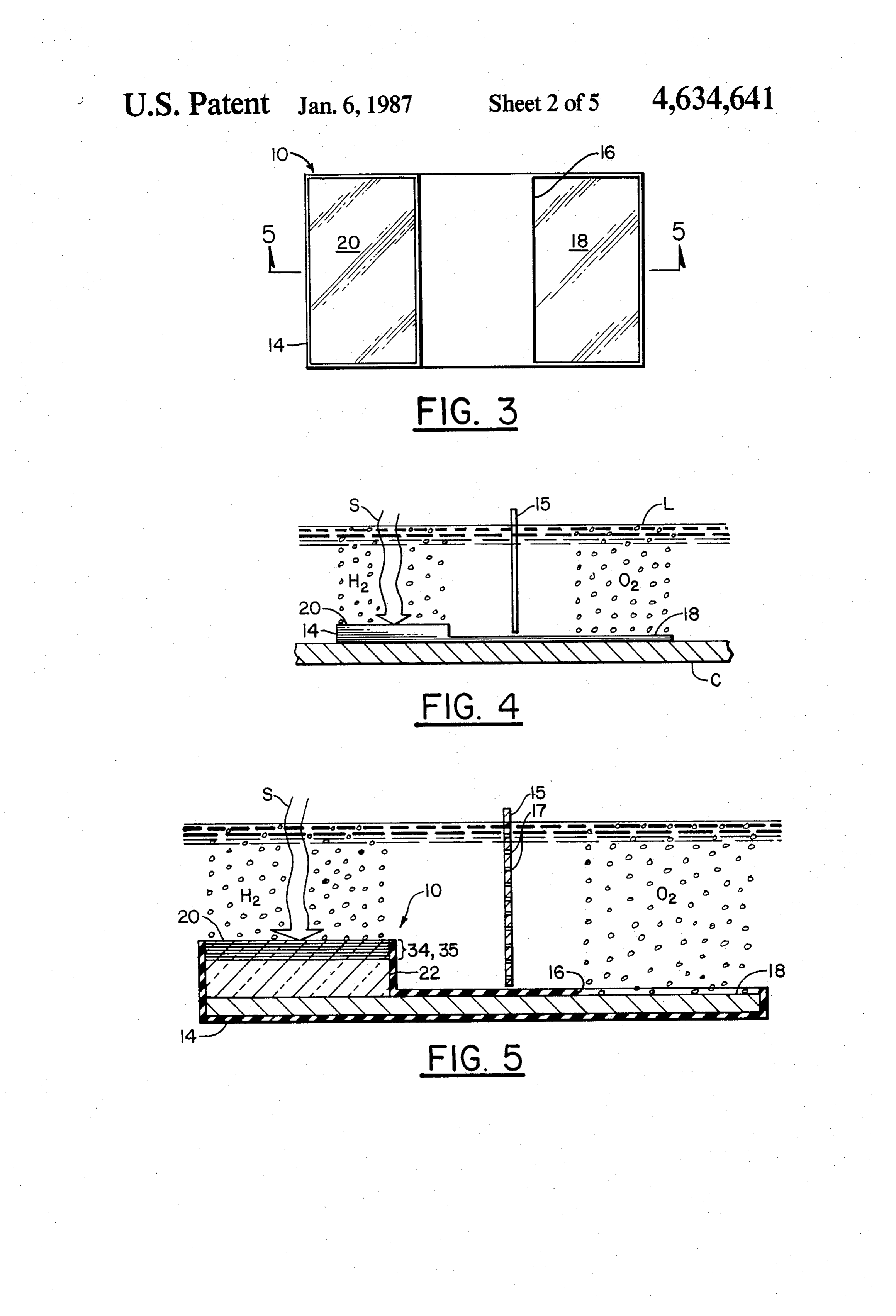
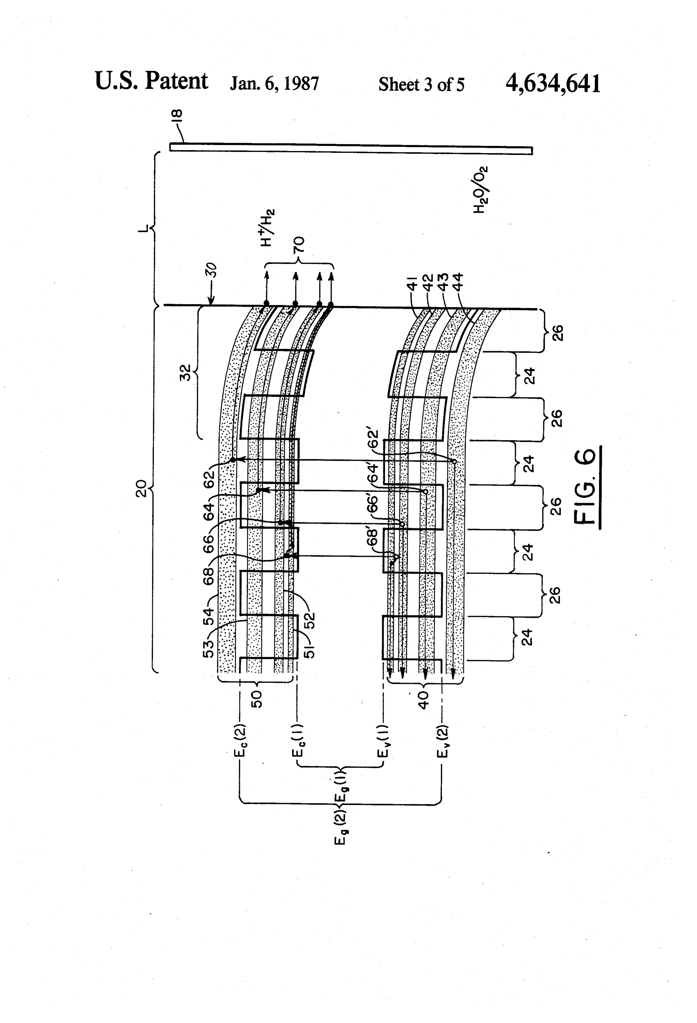
A further specific object of this invention is to pro the present invention shown immersed in a liquid elec vide a method for capturing and siphoning off hot carri trolyte and exposed to sunlight to produce the desired ers from a semiconductor prior to thermalization. redox chemical reactions;
A still further specific object of the present invention FIG. 5 is an enlarged cross-sectional view of the is to provide an efficient and effective photoelectro 5 multipled quantum well or superlattice photoelectro chemical electrode for electrolysis processes. chemical cell of the present invention shown immersed Another specific object of the present invention is to in an electrolyte liquid and exposed to sunlight; provide an efficient method and apparatus for injecting FIG. 6 is an energy level diagram of the superlattice hot carriers into an electrolyte for driving electrolysis photoelectrode of the present invention; processes. O FIG. 7 is an isometric view of an alternate embodi Still another specific object of the present invention is ment superlattice photoelectrochemical cell according to provide an electrode for a photoelectrochemical cell to the present invention;
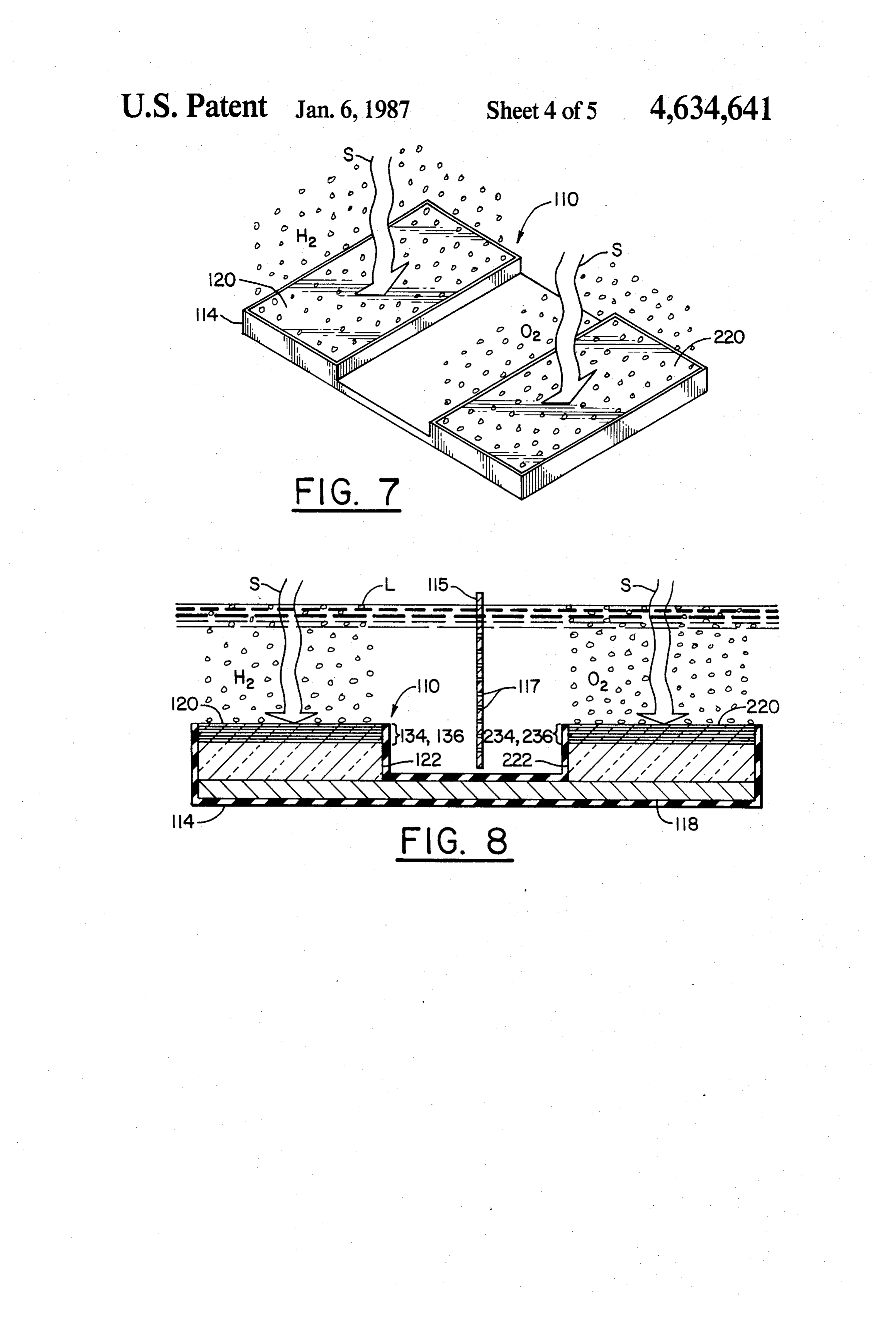
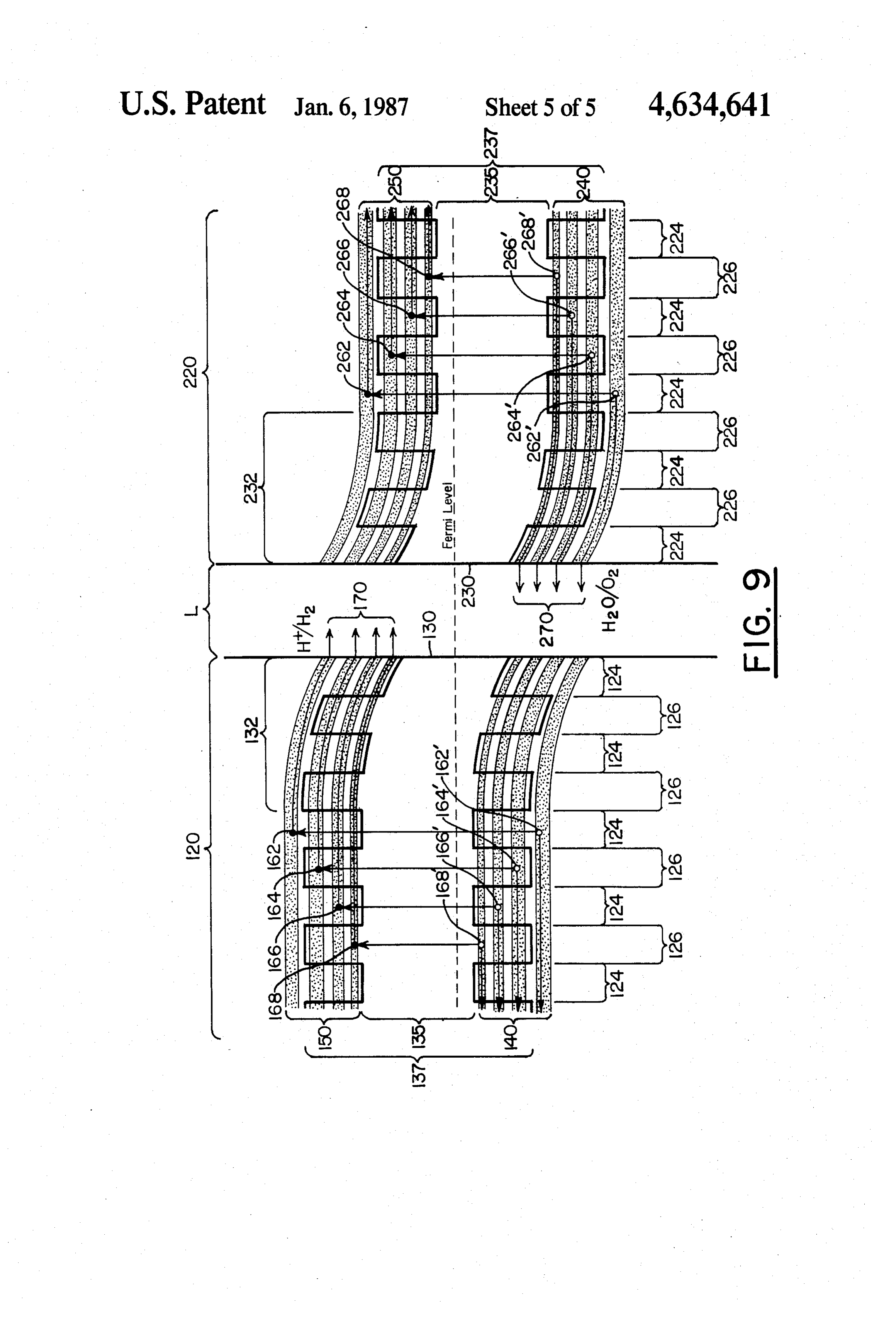
that is capable of capturing photons at discrete energy FIG. 8 is an enlarged cross-section of the alternate levels, creating charge carriers corresponding to such embodiment superlattice photoelectrochemical cell of discrete energy levels, and transferring such carriers 15 FIG. 7 shown immersed in an electrolyte and exposed essentially at those energy levels into an electrolyte to solar radiation; and solution to drive beneficial chemical reactions to pro FIG. 9 is an energy level diagram of the alternate duce useable fuels or chemicals. embodiment superlattice photoelectrochemical cell Yet another object of the present invention is to pro shown in FIGS. 7 and 8.
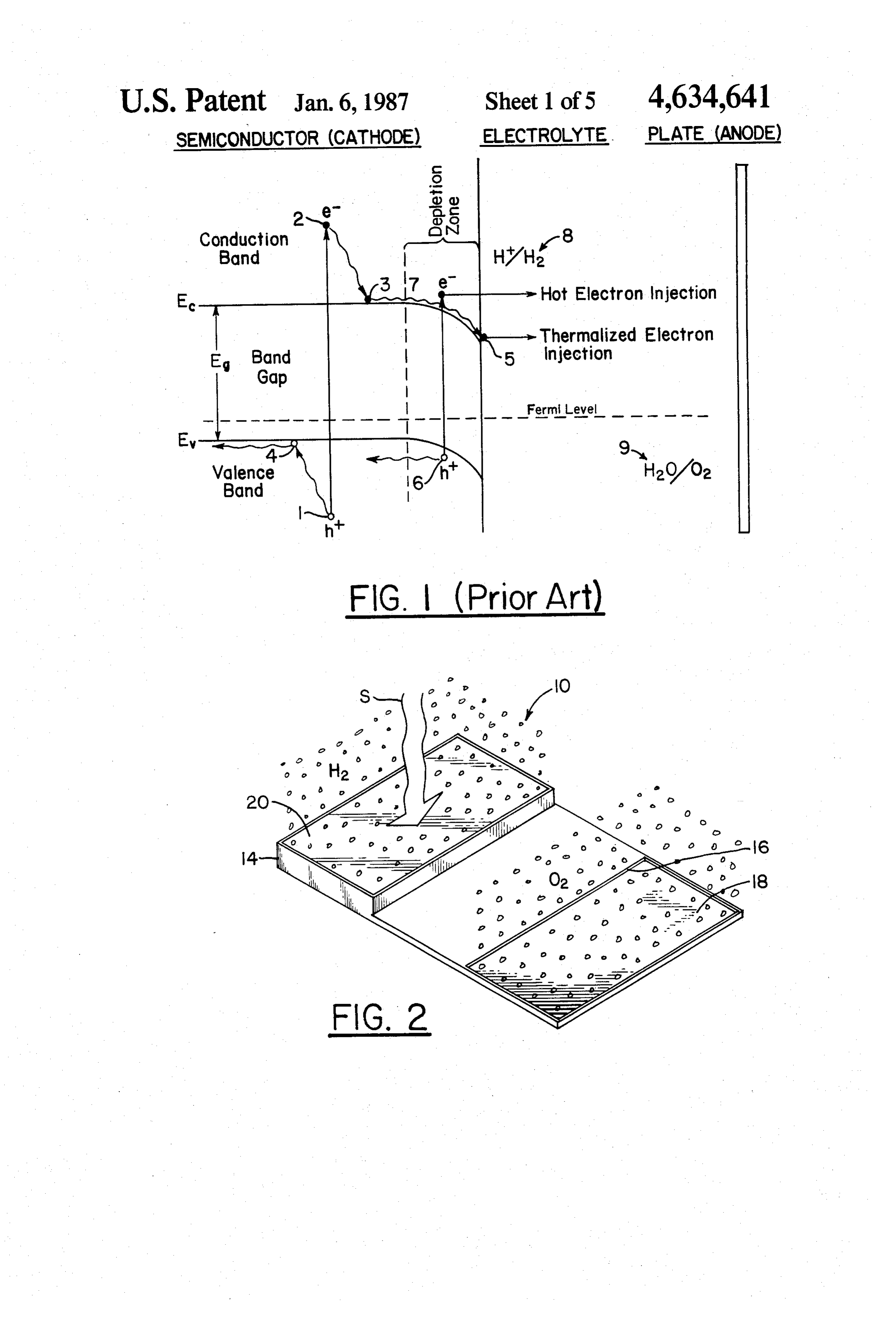
vide a method and apparatus for monitoring the basic 20 DETAILED DESCRIPTION OF THE properties of superlattice semiconductor devices. PREFERRED EMBODIMENT Additional objects, advantages, and novel features of the invention are set forth in part in the description that For the purposes of describing the present invention, follows, and in part will become apparent to those it is necessary to refer first to the prior art semiconduc skilled in the art upon examination of the following 25 tor electrodes utilized in photoelectrochemical cells. A specification or may be learned by the practice of the typical energy level diagram for such prior art photo invention. The objects and advantages of the invention electrochemical cells. is shown in FIG. 1. This energy may be realized and attained by means of the instrumen diagram is based on a typical p-type semiconductor it. talities and in combinations particularly pointed out in photoelectrode immersed in an electrolyte, such as wa : the appended claims. 30 ter, a spaced distance from a metal plate also immersed To achieve the foregoing and other objects and in in the electrolyte. The p-type semiconductor and the accordance with the purposes of the present invention, plate are connected electrically so that the p-type semi as embodied and broadly described herein, the method conductor functions as the cathode and the plate func and apparatus of this invention may comprise the use of tions as the anode in the photoelectrochemical conver a superlattice or multiple quantum well semiconductor 35 sion process.
as a photoelectrode in photoelectrochemical processes, As illustrated in FIG. 1, the energy band gap EGis the - such as for driving redox reactions in an electrolyte. distance between the upper edge of the valence band : The method may include immersing a superlattice or energy Evwith the lower edge of the conduction band ... multiple quantum well semiconductor in a liquid elec Ec. When a high-energy photon excites an electron 2 3. trolyte, coupling the superlattice or multiple-quantum 40 from the valence band to the conduction band, a posi : well semiconductor to an electrode or to another such tively charged "hole” 1 is left behind in the valence semiconductor also immersed in the electrolyte a band. Thus, the absorbed photon creates an electron spaced distance away, and exposing the semiconduc hole pair. The electron-hole pair 1, 2 illustrated in FIG. tor(s) to solar radiation to produce a photocurrent for 1 is a result of the electron having absorbed not only driving a chemical reaction, such as a redox chemical 45 enough energy from the photon to jump the band gap reaction. The apparatus includes the superlattice or Eg, but also enough energy to be excited to an energy multiple-quantum-well semiconductor(s) immersed in level in the conduction band much higher than the level an electrolyte. It also may include the electrode plate Ecat the bottom of the conduction band. Such an elec and conductors for directing the photocurrent to the tron excited to this high-energy level is called a "hot electrolyte and the redox couples therein. 50 electron', and the corresponding hole 1 is called a "hot hole'. Since both the hole 1 and the electron 2 are
BRIEF DESCRIPTION OF THE DRAWINGS charged carriers, such highly excited electron-hole The accompanying drawings, which are incorpo pairs are referred to as "hot carriers'.
rated in, and form a part of, the specification, illustrate These hot carriers are not in thermal equilibrium with the preferred embodiments of the present invention, and 55 the host lattice; thus they will remain at their high en together with the description, serve to explain the prin ergy level for a very short period, approximately a ciples of the invention. picosecond. Almost immediately, these hot carriers will In the drawings: give up their excess energy to the photons or vibrations FIG. 1 is an energy level diagram for a prior art of the crystal lattice in the form of heat. The result is photoelectrochemical cell; that the hot carriers 1, 2 relax almost immediately to the FIG. 2 is an isometric view of a multiple-quantum energy level Ecjust above the band gap, while giving well or superlattice photoelectrochemical cell accord up their excess energy as heat to the crystal lattice. This ing to the present invention; relaxation process is called thermalization of the hot FIG. 3 is a plan view of the multiple-quantum-well or carriers.
superlattice photoelectrochemical cell of the present 65 The local electrical field is caused by a depletion zone invention. adjacent the Schottky heterojunction at the interface of FIG. 4 is a side elevation view of the multiple-quan the semiconductor and electrolyte. This local electric tum-well or superlattice photoelectrochemical cell of field separates the electron-hole pairs and drives the
Page 11
electrons to the semiconductor/electrolyte interface layers are shown here as layers 34, 35, although in ac and the holes to the plate through an electrical connec tual practice a larger number of alternating layers is tion (not shown). In the electrolyte, redox couples such preferable. For example, in actual practice approxi as the hydrogen ion to hydrogen gas redox couple 8 and mately 20 layers is more practical. In this regard, it water to oxygen gas redox couple 9 are present and will should be mentioned that because these alternating lay absorb the charge carriers at the semiconductor/elec ers are extremely thin, usually in the range of 50 to 250 trolyte interface and the plate/electrolyte interface to angstroms, it is necessary for purposes of illustration drive the electrolysis reaction. and clarity to exaggerate the dimensions, particularly in The result of the thermalization of the excited elec the vertical direction. Therefore, it should be realized tron 2 to the bottom of the conduction EC is that the O that the illustrations for this invention, such as that energy derived from the semiconductor and available shown in FIG. 5, are not intended to, and in fact cannot for doing work in the electrolysis reaction is equal to practically be, exact proportional illustrations of the the band gap energy EG. The excess EG absorbed from semiconductor layers. It is expected that persons having the photon beyond the band gap energy EG is lost as ordinary skill in the art will understand the illustrations heat to the semiconductor lattice and is not available for 15 in this manner as represented in the accompanying use in the electrolysis process. drawings.
As discussed in the background section, there is some As shown in FIG. 5, when the superlattice semicon evidence that with highly doped semiconductors used ductor in combination with semiconductor/liquid or semicon potential20 or is exposed to solar radiation S, a photoelectric voltage is generated in the semiconductor ductor/solid interfaces, where large electric fields exist 20 20. The ohmic because of initial chemical potential differences be semiconductor plate 20 18 is connected electrically to the and has a portion exposed to the tween the phases, that hot electrons in the depletion electrolyte L through the zone above the band gap EG, as indicated at 6, 7, can be 14. A photoelectric currentopening is 16 in the insulation therefore generated in the injected as hot carriers at their higher-energy levels semiconductor 20 that flows through redox couples in directly into the electrolyte. However, since most of the the electrolyte L and the ohmic plate 18. In the
illustra thermalization of generated hot carriers occurs in the tion of FIG. 5, the top surface of the semiconductor 20 much larger bulk region of the semiconductor, where functions as the cathode, and the exposed surface of the the energy bands are flat, than in the small depletion ohmic plate 18 functions as the anode in the photoelec zones, where the band bending occurs, such hot elec trochemical process resulting in the production of hy tron ejection (known as type-I hot electrons) has not 30 drogen gas H2 and oxygen gas O2, which bubble off the been a significant factor in increasing photon conver sion efficiencies. surfaces of the semiconductor 20 and ohmic plate 18, The present invention, however, which includes mul respectively.
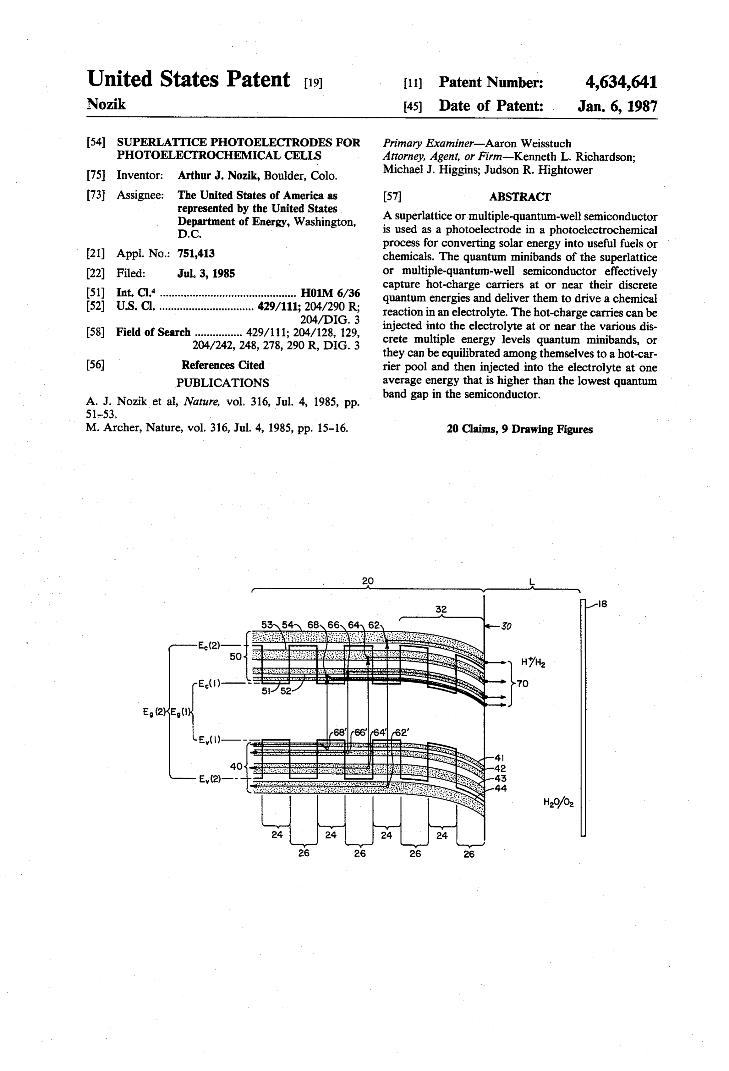
tiple-quantum-well or superlattice photoelectrochemi The energy diagram of FIG. 6 is used to describe in cal cell 10, is shown in FIG. 2. It comprises a multiple 35 more detail the functions and characteristics of the pres quantum-well or superlattice semiconductor 20 posi ent invention. As described briefly earlier, the superlat tioned on a plate 18 and encapsulated in an insulation tice semiconductor structure 20 comprises a substrate material 14, except for the top surface thereof, which is 22, preferably of some crystalline material, although left exposed. An opening 16 in insulation 14 exposes a recent advances in related fields are leading toward the portion of the plate 18. When the photoelectrochemical eventual feasibility of polycrystalline, amorphous, and cell 10 is immersed in a liquid electrolyte and exposed to other semiconductor materials for photocells as well. solar radiation S, the redox reaction occurs. The gases For purposes of describing this invention, but not for produced, such as hydrogen and oxygen from a water limitation, the substrate 22 is described as gallium arse electrolyte, bubble off the cathode and anode portions nide (GaAs) crystal. The alternating layers 34, 35 of the cell 10, as will be described in more detail below. 45 (shown in FIG. 5) are described as gallium arsenide The photoelectrochemical cell 10 of the present in (GaAs) and gallium arsenide phosphide (GaAsP1-x), vention is shown in plan view in FIG. 3, and it is shown respectively. The GaAs has a band gap Eg(1) of about in FIG. 4 immersed in a liquid electrolyte L, such as 1.3 eV and GaAsosPos has aband gap Eg(2) of about 2.5 water, in a container C. The hydrogen gas H2 and oxy eV. The resulting superlattice semiconductor 20 is a gen gas O2 bubbled off the cathode and anode portions 50 strained layer compositional superlattice. It is under of the cell 10 can be collected for use in ways well stood, of course, that other semiconductor materials can known to persons skilled in the art. As shown in FIGS. also be used and are preferably selected from Group III, 4 and 5, a semi-permeable membrane 15, having open Group IV and Group V semiconductor materials. ings 17 therethrough, is used to segregate the hydrogen The energy level diagram of FIG. 6 illustrates the and oxygen gases. The openings 17 are small enough to 55 composite effect of the alternating GaAs and exclude the gas bubbles from passing therethrough, but GaAso,5P05 layers 34, 35 with their different character the liquid and ionic charge carriers can easily pass istic band gaps Eg(1), Eg(2), respectively. Essentially, through the semipermeable membrane 15. the smaller band gaps Eg(1) of the GaAs layers 34 sand The structure of the photoelectrochemical cell 10 wiched between the larger band gaps Eg(2) of the according to the present invention is best seen in FIG. 5, GaAso.5P05 layers 35 form what are called energy which is an enlarged cross-section taken along lines “wells' 26 between energy “barriers" 24. Further, mini 5-5 of FIG. 3. As shown in FIG. 5, a multiple-quan bands of specific quantum energy levels are formed tum-well or superlattice semiconductor 20 is positioned within the wells 26. Such minibands 41, 42, 43, 44 below on an ohmic or metal plate 18. The semiconductor 20 the valence energy level E.(1) for the GaAs layers 34 preferably comprises a crystalline substrate 22 having 65 are referred to collectively as the valence minibands 40. deposited thereon alternating layers of different crystal Similarly, minibands 51, 52, 53, 54 above the conduction line semiconductor compositions having respectively energy level E-(1) for the GaAs layers 34 are referred to different band gap characteristics. Such alternating collectively as the conduction minibands 50.
Page 12
It was generally considered in the prior art that the band energy levels of the superlattice and vice versa, wells 26 in such semiconductor structures were elec thus even further increasing the efficiencies of solar tronically isolated from each other when the barriers 24 energy conversion according to this invention. Another were over 50 angstroms thick. Such semiconductor mode of hot carrier utilization in superlattice and multi structures with barriers 26 over 50 angstroms thick have ple-quantum-well electrodes is where the hot charge been generally referred to as "multiple-quantum-wells." carriers in the various minibands equilibrate among However, when the barriers 24 are less than 50 ang themselves to form a hot-carrier pool from which strons thick, electrons and holes can tunnel through the charge is then injected into the electrolyte at one higher barriers 24 from one well 26 to another. Thus, the mini average energy.
bands 40, 50 can extend through the barriers 24, to form 10 It is also appropriate to mention at this point that very conditnuous minibands through the bulk of the semi high charge carrier transfer efficiencies from the semi conductor, as shown in FIG. 6. Such semiconductor conductor to the electrolyte chemical reactions have structures having barriers 24 less then 50 angstrons been observed with this invention, even in multiple thick and having continuous minibands 40, 50 extending quantum well semiconductor structures having barrier from well to well 26 through the barriers 24 have been 15 24 thicknesses up to 250 angstroms. Such high carrier referred to in the prior art as "superlattice' semicon transfer efficiences were unexpected in structures hav ductors. ing barriers 24 thicker than the 50 angstroms maximum As discussed briefly in the background section, super barrier thickness associated in the prior art with super lattice semiconductors have some very unique and po lattice structures and is not yet fully explained. How tentially beneficial characteristics that have not been 20 ever, these results do call into question the prior art useable to any significant extent, particularly in solar 50-angstrom barrier thickness distinction between energy conversion applications, prior to this invention. superlattices and multiple-quantum-wells enough so Specifically, the minibands 40, 50 provide an ideal envi that, at least for the purposes of describing and claiming ronment for capturing and holding hot carriers for long this invention, strict adherence to that distinction is not periods, thus having the potential of substantially slow 25 necessary or helpful and will not be observed. In other ing or reducing thermalization of such carriers and the words, since the multiple-layered compositions or dop resulting loss of useable electrical energy as heat or ing semiconductors used with this invention seem to photons in the crystal lattice. Also, photon absorption is work as well with barriers 24 significantly over, as well is increased substantially where photon energies corre as under, 50 angstroms thick, the terms "superlattice" spond to the band gaps between pairs of valence and 30 and "multiple-quantum-well' are used interchangeably conduction minibands. Such electronic properties can in the remaining description and claims herein. be designed and tailored in superlattice structures by Referring now to FIGS. 5 and 6, the alternating lay varying the materials and thicknesses of the layers 34, ers 34, 35 of GaAs and GaAsosos, respectively, on the 35. GaAs substrate 22 create the superlattice or multiple Utilization of these characteristics is achieved in this 35 quantum-well semiconductor 20 with valence mini invention by using the superlattice semiconductors as bands 40 and conduction minibands 50. The valence ... photoelectrodes in photoelectrochemical electrolysis minibands 40 are illustrated in FIG. 6 as comprises four * processes. The specifics of such applications are de minibands 41, 42, 43, 44 and different energy levels scribed more fully below. However, it is appropriate to under the valence band edge E(1) of the GaAs layers mention at this point that such photoelectrochemical 34. Likewise, the conduction minibands 50 are illus * processes according to this invention use the internal trated in FIG. 6 as comprises four minibands 51, 52, 53, photoinduced electric current in driving chemical reac 54, each of which corresponds to a respective one of the tions rather than siphoning the charge carriers off the valence minibands 41, 42, 43, 44. semiconductor in a conventional manner through elec As mentioned previously, the sizes and energy levels trodes or electrical conductors attached to the semicon 45 of the minibands are functions of the compositions and ductors to some external electrical load. In fact, one of thicknesses of the layers 34,35. This type of superlattice the impediments of fully utilizing the advantageous is known as a compositional superlattice. Other kinds of characteristics of superlattice semionductors prior to superlattice structures known in the art can also be this invention was that no solid energy sensitive elec used; for example, a doping superlattice (not shown), trode or conductor was capable of drawing the charge 50 consisting of an array of layers of the same semiconduc carriers off a superlattice semiconductor at the various tor materials doped in different ways, can also be used individual discrete miniband energy levels for use in in this invention. Further, compositional superlattices, external electric loads at those various discrete energy such as that illustrated in FIG. 6, can also be doped to levels. increase the mobility of electrons, as will be apparent to In the present invention, however, chemical reactions 55 persons skilled in the art in view of this invention. can and do occur at different energy levels. Therefore, Therefore, while the description of this invention is according to this invention, the electron and hole primarily based on a compositional superlattice photo charge carriers can be drawn off at different energy electrode, it should be understood that references to levels in chemical reactions. Thus, photon energy that superlattices herein can apply to other types of superlat produces hot carriers can be utilized at the respective tice semiconductors as well.
discrete energy levels of the hot carriers by selectively As shown in FIGS. 5 and 6, the superlattice semicon drawing the hot carriers off the superlattices at their ductor 20 is immersed in the liquid electrolyte L, respective discrete miniband levels to produce hydro thereby creating a heterojunction at the interface 30 gen and oxygen gases. The results is very minimal en between the exposed surface of the semiconductor 20 ergy loss caused by thermalizing of hot carriers in the 65 and the liquid electrolyte L. Such a semiconductor/liq superlattice semiconductor. Further, the energy levels uid heterojunction is in the nature of a Schottky hetero of the acceptor electrolytes or redox couples can be junction and creates a depletion zone 32 adjacent the adjusted by turning the chemical reactions to the mini interface 30, which results in a local electric field that
Page 13
bends the energy levels and corresponding minibands corresponding holes 66, 64", 62 are driven in the oppo 40, 50 in the depletion zone. This local electric field in site direction to the plate 18. the depletion zone is effective to separate the electron Any electrons (not shown) that are photoexcited hole pairs produced by photon absorption and drives an above or between minibands will relax or thermalize electric current to the electrolysis couples, such as the only to the next lower miniband where they will be redox couples described above. captured and delivered to the interface 30 at the energy When the surface of the superlattice semiconductor level of that miniband. Thus, again, energy loss by hot 20 is exposed to solar radiation, as illustrated in FIGS. 2, electrons can be minimized significantly by superlattice 4, and 5, photons of solar energy are absorbed by va structures designed or tailored to provide miniband lence band electrons. If the energy absorbed by one 10 energy levels that conform as nearly as possible to the electron is sufficient, it will be excited enough to jump photon energy levels that constitute the solar radiation the band gap from the valence band to the conduction S being absorbed by the semiconductor 20. band. In a superlattice, the absorbed energy must be At the interface 30, the electrons 70, 70, 70, 70 are enough to excite the electron to jump from a valence injected into the electrolyte L to drive the redox elec miniband to a conduction miniband. Thus, as illustrated 15 trolysis chemical reaction. As mentioned briefly earlier, in FIG. 6, the energy absorbed by a valence electron, the H/H2 redox couple receives electrons and the such as electron 68, must be at least enough for the H2O/O2 redox couple receives holes to produce hydro electron 68 to jump the gap between the closest valence gen and oxygen gases. As also mentioned briefly earlier, and conduction minibands 41, 51, respectively. If there redox couples can receive and utilize electrons and is insufficient energy absorbed by the electron to jump 20 holes at multiple energy levels to drive the chemical that smallest miniband gap, the photon is not absorbed reactions. Thus, the solar energy absorbed by the super and therefore does not contribute to the energy conver lattice semiconductor 20 can be converted to useable sion process. On the other hand, if the electron 68 makes chemicals or gases at much higher-efficiency levels the jump from the valence miniband 41 to conduction according to this invention than was possible in the miniband 51, it will be captured by the conduction mini 25 prior art. Further, the use of superlattice photoelec band 51 and pulled by the local electric field in the trodes in combination with electrochemical reactions depletion zone toward the interface 30, as illustrated at according to this invention provides a mechanism for 70 in FIG. 6. Simultaneously, the corresponding hole extracting and utilizing hot-charge carriers from super 68 is driven in the opposite direction away from the lattices at or near their respective discrete miniband interface 30. 30 energy levels for solar energy conversion, which was As shown in FIG. 5, the ohmic plate 18 is contacted not possible prior to this invention.
to the substrate 22 and exposed to the electrolyte L a It should be mentioned that this invention contem spaced distance from the superlattice semiconductor 20. plates the use of superlattice photoelectrodes in electro The hole 68' is therefore effectively transferred to the chemical voltaic cells wherein there is only one effec plate 18 where it is available for the redox couple H2O 35 tive redox couple and the net free energy change in the /O2. The electrical connection between the superlattice electrolyte is zero, as well as in photoelectrosynthesis 20 and the plate 18 could also be made via wire or other cells wherein two effective redox couples are present in contacts or carrier transfer structures known to persons the electrolyte and a net chemical change occurs. It also skilled in the art. Since the illustration in FIG. 6 is in contemplates the use of superlattice photoelectrodes in tended primarily as an energy diagram, no contact or all three types of photoelectrosynthesis cells known in carrier transfer structure for conducting the charge the prior art as photoelectrochemical cells, photoelec carriers between the superlattice 20 and the plate 18 is trolysis cells, and photocatalysis cells. shown, but such structure is assumed to be present, as One specific example of a compositional superlattice shown in FIG. 5, to complete the electric circuit. semiconductor structure that is satisfactory for use as a If the electron 68 absorbs more energy from a photon 45 photoelectrode according to this invention is a strained than is necessary to jump the band gap between the layer superlattice prepared on a p-GaAs crystalline closest valence and conduction minibands 41, 51, re substrate with a 10-micron GaAs1-P buffer layer spectively, but not enough to jump the band gap be graded from X=0.05 to 0.25. There can be about 20 tween the next closest valence and conduction mini alternating layers of GaAs and GaAso,05P05 prepared bands 42, 52, respectively, as illustrated in FIG. 6, it will 50 by metallorganic chemical vapor deposition using con merely relax or thermalize down to the conduction ventional deposition techniques. Each layer can be in miniband 51. Thus, a small amount of energy is lost to the range of approximately 50 to 250 angstroms thick. the lattice by thermalization. However, capture of the The electrolyte can be prepared as a solution containing electron by the next lower miniband 51 minimizes such 0.2M ferricyanide in 1M H2SO4 or 0.1M Eu3- in 1M thermalization energy loss. 55 HClO4.
The electrons 66, 64, 62 shown in FIG. 6 are illus Another embodiment of a photoelectrochemical cell trated to have absorbed respectively higher-energy 110 according to the present invention is shown in photons, exciting them to jump larger miniband gaps to FIGS. 7-9. In this embodiment 110, there are two be captured in respectively higher-energy conduction superlattice semiconductors 120, 220, both of which minibands 52, 53, 54. These "hot electrons' 66, 64, 62 have substrates 122, 222, respectively, contacted to a are likewise driven by the electric field in the depletion common plate 118. In this embodiment, the surface of Zone in their respective discrete miniband energy levels the second semiconductor 220, rather than the surface to the interface 30, as illustrated at 70, 70, 70, respec of the plate 118, is exposed to the electrolyte L. The tively. Therefore, most of the energy absorbed by these superlattice semiconductor 120 illustrated in FIGS. 7-9 "hot electrons' from higher-energy photons is con 65 is constructed essentially like that described for the served and delivered at the energy levels of the respec preferred embodiment superlattice 10 described above. tive conduction minibands 52, 53, 54 to the electrolyte The superlattice semiconductor 120 comprises alternat L at the interface 30. Simultaneously, of course, the ing compositional or doping layers 134, 136 deposited
Page 14
on the substrate 122. Likewise, the superlattice semicon time, the local electric field 232 in the superlattice semi ductor 220 comprises a plurality of alternating layers of conductor 220 drives the holes 262", 264', 266, 268 to compositional or doping layers 234, 236 deposited on a the interface 230 where they are injected at their respec substrate 222. The compositional layers 134, 136 have tive discrete energy levels into the electrolyte L, as respective characteristic band gaps 135, 137, as illus- 5 indicated at 270. The electrons 170 and holes 270 in trated in FIG. 9. These respective band gaps 135,137 of jected into the electrolyte are received by the redox the alternating layers 134, 136 form the energy level couples H+/H2 and H2O/O2 to drive the chemical quantum wells 126 and barriers 124, resulting in the reactions that produce hydrogen and oxygen gases. valance minibands 140 and conduction minibands 150, One of the advantages of this embodiment is that it as shown in FIG. 9. O maximizes solar absorption area in the photoelectro Likewise, the superlattice semiconductor 220 com chemical cell 110, thus increasing solar radiation con prises alternating compositional layers 234, 236 having version efficiencies. Specifically, rather than having an respective band gaps 235, 237. These alternating layers inert portion of the plate 18 exposed to solar radiation as and respective band gaps form the energy level quan in the preferred embodiment cell 10 described above, tum wells 226 and barriers 224, resulting in the valence 15 this embodiment cell 110 has a second superlattice semi minibands 240 and conduction minibands 250. conductor 220 exposed to the solar radiation S in the In this photoelectrochemical cell embodiment 110, same area. The two superlattice semiconductors 120, the respective superlattice semiconductors 120, 220 are 220 then combine in series as shown in FIG. 9 and de preferably doped differently so that one of the semicon scribed previously to generate an electric current ductors is a net p-type doped superlattice and the other through the photoelectrochemical cell 110 to drive the is a net n-type superlattice. In the illustration of FIG. 9, redox chemical reactions in the electrolyte. The in the superlattice semiconductor 120 is illustrated to be a creased electric current resulting from the two superlat net p-type doped superlattice semiconductor, and the tice semiconductors 120, 220 coupled in series produces superlattice semiconductor 220 is illustrated to be a net more chemical product for the same cell area. n-type doped superlattice semiconductors. Both super 25 The foregoing description is considered as illustrative lattice semiconductors 120 and 220 are immersed in the liquid electrolyte L a spaced distance from each other. only of the principles of the invention. Further, since Therefore, the superlattice semiconductor 120 forms an numerous modifications and changes will readily occur to those skilled in the art, it is not desired to limit the interface 130 with the electrolyte L, and the superlattice invention to the exact construction and processes semiconductor 220 forms an interface 230 with the elec shown and described above. Accordingly, all suitable . . trolyte L at their respective exposed compositional ... layer surfaces. modifications and equivalents may be resorted to falling As further shown in FIG.9, the semiconductor-liquid within the scope of the invention as defined by the heterojunction interface 130 with the p-type doped claims The that follow.
embodiments of the invention in which an exclu semiconductor 120 results in a depletion zone 132 have 35 sive property or privilege is claimed are defined as ing an electric field therein that bends the energy mini abands downward. On the other hand, the semiconduc follows:
...tor-heterojunction at the interface 230 of the n-type first1. photoelectrode
Photoelectrochemical cell apparatus, comprising means for injecting charge carriers doped superlattice semiconductor 220 results in a deple into an electrolyte and second electrode means for in tion zone 232 with an electric field therein that bends 40 ...the energy bands 240, 250 upward. The result of this jecting oppositely charged carriers into the electrolyte, said first electrode means including a superlattice semi construction is that when the outer layers of both super conductor.
lattice semiconductors 120, 220 are exposed to solar S
radiation, as illustrated in FIGS. 7 and 8, they generate 2. The apparatus of claim 1, wherein said superlattice a net electrical current flowing in the same direction. 45 semiconductor includes a crystalline substrate with a Specifically, as shown in FIG. 9, photon absorption by plurality of ultrathin alternating layers of semiconduc the superlattice semiconductor 120 causes valence elec tor materials having different band gap energy levels trons, represented in FIG. 9 by electrons 162, 164, 166, deposited thereon, and said cell includes electrical 168 to jump the band gaps between the respective mini contact means for electrically connecting said superlat bands 140, 150 corresponding with the energy levels of 50 tice semiconductor to said second electrode means. the photons absorbed. The local electric field and the 3. The apparatus of claim 2, wherein said semicon depletion zone 132 drives the electrons 162164, 166,168 ductor is enclosed in an insulation material except for in the respective conduction minibands 150 to the semi the outermost layer, which outermost layer and said conductor-liquid interface 130 where they are injected second electrode means are exposed to an electrolyte at their respective discrete energy levels into the elec 55 and to solar radiation.
trolyte L as shown at 170. At the same time, the result 4. The apparatus of claim 3, wherein said second ing respective holes 162", 164, 166, 168' are driven in electrode means includes a metal plate electrically con the opposite direction through the plate 118 to the nected to said superlattice semiconductor on a side superlattice semiconductor 220. thereof opposite said outermost layer that is exposed to At the same time, photons absorbed by the superlat said electrolyte.
tice semiconductor 220 cause electrons therein, repre 5. The apparatus of claim 3, wherein said second sented in FIG.9 by electrons 262,264, 266,268, to jump electrode means includes a second superlattice semicon the respective band gaps to the conduction minibands ductor having one side thereof exposed to said electro 250 corresponding to the energy absorbed by each from lyte and to said solar radiation and the opposite side the photons. The local electric field 232 in superlattice 65 electrically connected to said first electrode means 220 then drives the electrons 262, 264, 266, 268 away superlattice semiconductor.
from the interface 230 and through the metal conductor 6. The apparatus of claim 5, wherein one of said first 118 to the superlattice semiconductor 120. At the same and second superlattice semiconductors is a net p-type.
Page 15
doped semiconductor and the other of said superlattice 15. The method of claim 12, including the steps of semiconductors is a net n-type doped semiconductor. using a first superlattice semiconductor as a cathode and 7. The aparatus of claim 1, wherein said superlattice a second superlattice semiconductor as an anode in said semiconductor is a compositional superlattice. photoelectrochemical cell.
8. The apparatus of claim 1, wherein said superlattice 16. The method of claim 15, including the steps of semiconductor is a strained layer compositional super using a net p-type doped superlattice semiconductor as lattice. the cathode and a net n-type doped semiconductor as 9. The apparatus of claim 1, wherein said superlattice the anode, and electrically coupling said two superlat semiconductor is a doping superlattice. tice semiconductors by a conductor connected to the 10. The apparatus of claim 1, wherein said superlat 10 positive side of the p-type semiconductor and to the tice semiconductor is formed from materials selected negative side of the n-type semiconductor and interfac from the group consisting of Group III, Group IV, and ing the other sides of said superlattice semiconductors Group V semiconductor materials, said semiconductor with an electrolyte.
materials being chosen to provide said first electrode 17. The method of claim 16, including the steps of means with a plurality of discrete miniband energy 5 coupling said other sides of said superlattice semicon levels capable of capturing and injecting hot carriers ductors with redox couples in said electrolyte. into said electrolyte near the discrete energy levels at 18. The method of claim 12, including the steps of which said hot carriers are initially photoexcited upon forming the superlattice semiconductor with alternating exposure of said superlattice semiconductor to solar layers of semiconductor materials having different band radiation. 20 gap energy levels to produce discrete miniband energy 11. Th apparatus of claim 10, wherein said superlat levels therein capable of capturing hot-charge carriers tice semiconductor is formed from alternating layers of at or near their initial photoexcited quantum energy semiconductor materials having different band gap en levels, equilibrating such hot-carriers among themselves ergy levels to produce said miniband energy levels, said thereby forming a hot carrier pool at an energy quan aternating layers being in the range of 50 angstroms 250 25 tum above the smallest miniband gap, and injecting said to angstroms thick. hot-charge carriers into the electrolyte at or near the 12. A method of converting solar radiation to alter energy quantum of said hot-carrier pool. nate useable energy forms, comprising the steps of using 19. The method of extracting hot carriers from multi a superlattice semiconductor as a photoelectrode in a ple minibands of a superlattice semiconductor for per photoelectrochemical cell and exposing said superlat 30 forming useful work at or near the discrete energy lev tice semiconductor to solar radiation to produce a pho els of such minibands, comprising the steps of utilizing toelectric current to drive a chemical reaction in the the superlattice semiconductor as a photoelectrode in a photoelectrochemical cell. photoelectrochemical cell to drive a chemical reaction 13. The method of claim 12, including the steps of by injecting the hot carriers into an electrolyte in the forming the superlattice semiconductor with alternating 35 photoelectrochemical cell.
layers of semiconductor materials having different band 20. The method of claim 19, including the steps of gap energy levels to produce discrete miniband energy coupling the superlattice semiconductor with another levels therein capable of capturing hot carriers near electrode in the photoelectrochemical cell by connect their initial photoexcited quantum energy levels and ing a conductor to one side of said superlattice semicon injecting them at approximately those quantum energy 40 ductor and to said other electrode and immersing said - levels into said chemical reaction. interfacing the opposite side of the superlattice semicon 14. The method of claim 13, including the steps of ductor and said other electrode with an electrolyte tuning the photoelectrochemical cell by providing having chemical reaction couples capable of receiving chemical reaction couples capable of accepting and and utilizing hot carriers at or near the discrete energy utilizing said hot carriers near said discrete quantum 45 levels of said minibands.
energy levels. sk k k is
Provenance
- Collection
- Cited prior art
- Original PDF
- patentimages.storage.googleapis.com →
- Filed
- 1985-07-03
- Pages
- 15
- Method
- pdftotext (the PDF's own text layer) + pdftoppm 300dpi page scans
- Source
- Google Patents bibliographic record
- Granted
- 1987-01-06
- Inventors
- Arthur J. Nozik; US Department of Energy
- Transcribed from
- patentimages.storage.googleapis.com →