patent · US6281426
Multi-junction, monolithic solar cell using low-band-gap materials lattice matched to GaAs or Ge
28 August 2001
Page 1 — bibliographic record
(12) United States Patent (10) Patent No.: US 6,281,426 B1 Olson et al. (45) Date of Patent: Aug. 28, 2001
(54) MULTI-JUNCTION, MONOLITHIC SOLAR 5,316,593 5/1994 Olson et al. ......................... 136/262 CELLUSING LOW-BAND-GAP MATERLALS 5,322.572 * 6/1994 Wanlass ...... ... 136/249 LATTICE MATCHED TO GAAS OR GE 5,405,453 * 4/1995 Ho et al -- --- ---------- --- ------------ 136/249 5,407,491 4/1995 Freundlich et al. ................. 136/249 (75) Inventors: Jerry M. Olson, Lakewood; Sarah R. 5,944.913 8/1999 Hou et al. ............................ 136/255 Kurtz, Golden; Daniel J. Friedman, * cited by examiner
Lakewood, all of CO (US)
Primary Examiner Mark Chapman (73) ASSignee: Miss, such Institute, Kansas (74) Attorney, Agent, or Firm-Paul J. White
(*) Notice: Subject to any disclaimer, the term of this (57) patent is extended or adjusted under 35 A multi-junction, monolithic, photovoltaic Solar cell device U.S.C. 154(b) by 0 days. is provided for converting Solar radiation to photocurrent and photovoltage with improved efficiency. The Solar cell (21) Appl. No.: 09/615,297 device comprises a plurality of Semiconductor cells, i.e., active p/njunctions, connected in tandem and deposited on (22) Filed: Jul. 13, 2000 a Substrate fabricated from GaAS or Ge. To increase efficiency, each Semiconductor cell is fabricated from a
Related U.S. Application Data crystalline material with a lattice constant Substantially equivalent to the lattice constant of the Substrate material.
(63) still priation No. 09/165,039, filed on Oct. 1, Additionally, the Semiconductor cells are Selected with
1997. Ration No. 60060720, filed on oct. 1 appropriate from a largerband gapsof totheefficiently portion createInphotovoltage
Solar spectrum. this regard, 7 one Semiconductor cell in each embodiment of the Solar cell (51) Int. Cl.' ..................................................... H01L 25/00 device has a band gap between that of Ge and GaAS. To (52) U.S. Cl. ........................... 136/249; 136/261; 136/262 achieve desired band gapS and lattice constants, the Semi (58) Field of Search ..................................... 136/249, 261, conductor cells may be fabricated from a number of mate 136/262 rials including Ge, GainP, GaAs, GainASP, GainASN,
GaASGe, BGalnAS, (GaAs)Ge, CuInSSe, CuASSSe, and (56) References Cited GainASNP. To further increase efficiency, the thickness of
current generated in each cell. To facilitate photocurrent 4,179,702 12/1979 Lamorte ................................. 357/30 flow, a plurality of tunnel junctions of low-resistivity mate 4,206,002 * 6/1980 Sabnis et al. . 136/89 MS rial are included between each adjacent Semiconductor cell. 4,667,059 * 5/1987 Olson ............ ... 136/249 The conductivity or direction of photocurrent in the solar 4,867,801 * 9/1989 Stanbery ... ... 136/249 cell device may be Selected by controlling the Specific p-type 4.915,744 * 4/1990 Ho et al. ... ... 136/262 or n-type characteristics for each active junction. 5,009,719 * 4/1991 Yoshida ......... ... 136/249 5,223,043 * 6/1993 Olson et al. .. ... 136/249 5,261,969 * 11/1993 Stanbery .............................. 136/249 44 Claims, 3 Drawing Sheets
Page 2
Drawing sheet — no readable text.
Page 3
Drawing sheet — no readable text.
Page 4
Drawing sheet — no readable text.
Page 5
MULTI-JUNCTION, MONOLITHIC SOLAR differently-configured Semiconductor layers with two or CELLUSING LOW-BAND-GAP MATERIALS more Solar energy conversion junctions, each of which is LATTICE MATCHED TO GAAS OR GE designed to convert a different Solar energy or wavelength band to electricity. Thus, Solar energy in a wavelength band
CROSS-REFERENCE TO RELATED that is not absorbed and converted to electrical energy at one APPLICATION Semiconductor junction may be captured and converted to electrical energy at another Semiconductor junction in the
This patent application is a continuation of copending Solar cell that is designed for that particular wavelength
Patent and Trademark Office on Oct. 1, 1998, now aban Several difficulties have arisen in producing these multi doned which claimed the benefit of priority under 35 U.S.C. junction Solar cells which has limited their energy conver $119 to U.S. Provisional Patent Application No. 60/060,729 sion efficiency. First, it has proven difficult to fabricate each filed on Oct. 1, 1997. Semiconductor junction So as to maintain high photovoltaic CONTRACTUAL ORIGIN OF THE INVENTION device quality and Simultaneously the appropriate band 15 Structure, electron energy levels, conduction, and
The United States Government has rights in this invention absorption, that provide the photovoltaic effect within the under Contract No. DE-AC36-99GO 10337 between the Solar cell as the multiple layers of different Semiconductor United States Department of Energy and the National materials are deposited to form the Solar cells. It is under Renewable Energy Laboratory, a Division of the Midwest stood that photovoltaic quality may be improved in mono Research Institute. lithic Solar cells by lattice matching adjacent layers of
BACKGROUND OF THE INVENTION
Semiconductor materials in the Solar cell, meaning that each crystalline Semiconductor material that is deposited and 1. Field of the Invention grown to form the Solar cell has similar crystal lattice The present invention relates generally to photovoltaic constants or parameters. Mismatching at the Semiconductor Solar cells, and, more particularly, to a high-efficiency, 25 junctions in the Solar cells continues in many fabricated multi-junction, lattice-matched, monolithic Solar cell device. Solar cells to create defects or dislocations in the crystal Even more particularly, the present invention is directed to lattice of the Solar cell, which causes degradation of critical photovoltaic quality characteristics, Such as open-circuit a Solar cell device that includes a Semiconductor cell that is lattice-matched to GaAS and has an optimal band gap for Voltage, short-circuit current, and fill factor. Second, the enhancing the energy conversion efficiency of the Solar cell energy conversion efficiency, including photocurrent and photovoltage, has proven difficult to maximize in multi device.
2. Description of the Prior Art junction Solar cells. Photocurrent flow can be improved if each Solar cell junction of the Semiconductor device can be
Solar energy is an important Source of energy. Photovol current matched, in other words, to design each Solar cell taic devices fabricated from layers of Semiconductor 35 junction in the multi-junction device in a manner Such that materials, commonly called Solar cells, are presently used to the electric current produced by each cell junction in the convert Solar energy directly into electricity for many elec device is the Same.
trically powered applications. However, greater Solar energy Current matching is important when a multi-junction Solar to electrical energy conversion efficiencies are Still needed in cell device is fabricated with the individual semiconductor Solar cells to bring the cost per watt of electricity produced 40 cells in the device connected (i.e., Stacked) in Series, into line with the cost of generating electricity with fossil because, in a Series circuit, current flow is limited to the fuels and nuclear energy and to lower the cost of telecom Smallest current produced by any one of the individual cells munication Satellites.
in the device. Current matching can be controlled during
Solar energy, essentially light, comprises electromagnetic fabrication by Selecting and controlling the relative band gap radiation in a whole spectrum of wavelengths, i.e., discrete 45 energy absorption capabilities of the various Semiconductor particles or photons at various energy levels, ranging from materials used to form the cell junctions and the thicknesses higher energy ultraviolet with wavelengths less than 390 nm of each Semiconductor cell in the multi-junction device. In to lower energy near-infrared with wavelengths as long as contrast, the photovoltages produced by each Semiconductor 3000 nm. Between these ultraviolet and infrared wave cell are additive, and preferably each Semiconductor cell lengths or electromagnetic radiation energy levels are the 50 within a multi-cell Solar cell is Selected to provide Small Visible light spectrum, comprising Violet, blue, green, increments of power absorption (e.g., a Series of gradually yellow, orange, and red wavelengths or energy bands. reducing band gap energies) to improve the total power, and Because a Semiconductor layer of a Solar cell absorbs Specifically the Voltage, output of the Solar cell. photons with energy greater than the band gap of the To address the above fabrication problems, a large num Semiconductor layer, a low band gap Semiconductor layer 55 ber of materials and material compounds have been utilized absorbs most of the photons in the received Solar energy. in fabricating multi-junction, monolithic Solar cell devices. However, useful electrical power produced by the solar cell However, these prior art Solar cells have often resulted in is the product of the Voltage and the current produced by the lattice-mismatching, which may lead to photovoltaic quality Solar cell during conversion of the Solar energy to electrical degradation and reduced efficiency even for Slight energy. Although a Solar cell made from a low band gap 60 mismatching, Such as less than 1 percent. Further, even when material may generate a relatively large current, the Voltage lattice-matching is achieved, these prior art Solar cells often is often undesirably low for many implementations of Solar fail to obtain desired photovoltage outputs. This low effi cells. ciency is caused, at least in part, by the difficulty of To achieve the goal of using most of the photons in the lattice-matching each Semiconductor cell to commonly used Solar spectrum while Simultaneously achieving higher out 65 and preferred materials for the Substrate, Such as germanium put voltage, multi-junction Solar cells have been developed. (Ge) or gallium-arsenide (GaAS) Substrates. AS discussed Multi-junction Solar cells generally include multiple, above, it is preferable that each Sequential junction absorb
Page 6
energy with a slightly Smaller band gap to more efficiently Semiconductor cell to allow photocurrent to flow readily convert the full spectrum of Solar energy. In this regard, Solar between the Semiconductor cells and is Substantially a cells are Stacked in descending order of band gap energy. highly-doped Semiconductor with very low resistance to However, the limited selection of known semiconductor current flow.
materials, and corresponding band gaps, that have the same In one embodiment, a two-junction Solar cell is provided lattice constant as the above preferred Substrate materials which comprises a bottom junction of GainASN or GaAsGe has continued to make it difficult to design and fabricate a material on the GaAS or Ge Substrate and a top junction of multi-junction, monolithic Solar cell that efficiently converts GainASP material above the bottom junction. A second the received Solar radiation to electricity. Therefore, a need embodiment is a three-junction Solar cell which includes an remains to provide Semiconductor materials with desirable additional junction of Ge material underneath the bottom band gap ranges and with a lattice constant that is Substan junction of the first embodiment. In a third embodiment, a tially equivalent to that of Ge or GaAS to improve prior art three-junction Solar cell is provided which comprises a photovoltage output and Solar energy conversion efficiency bottom junction of GainASN or GaASGe material on the for Solar cells. GaAS or Ge Substrate, a middle junction of GaAS material, 15 and a top junction of GalnP material. A fourth embodiment
SUMMARY OF THE INVENTION
provides a four-junction Solar cell with, in descending order,
Accordingly, it is a general object of the present invention a first junction of Ganp, a Secondjunction of GaAS material, to provide a more efficient multi-junction, photovoltaic Solar a third junction of GainASN or GaASGe material, and a cell device than has been heretofore been available. fourth junction of Ge material on a Ge Substrate. In the It is a Specific object of the present invention to provide above embodiments, each junction may be a n-on-p or a a high-efficiency, multi-junction, monolithic Solar cell p-on-n type. Each junction is formed by a different arrange device in which each Semiconductor cell or junction is ment of n-type and p-type material layers; the Specific p-type fabricated from crystalline materials having Substantially the or n-type conductivity for each active junction is established Same lattice constant and is photocurrent matched. by the conductivity characteristics of the Selected material It is a related Specific object of the present invention to 25 layers. Additional layerS may be included as part of each provide a high-efficiency, multi-junction, monolithic Solar junction, in accordance with Standard practice, to reduce cell with lattice and current matching in which GaAS or Ge problems Such as photocarrier recombination. Also, addi is used as a growth Substrate of the Solar cell. tional layerS may be added to each Solar cell to control A further specific object of the present invention is to reflectivity within the Solar cell. Further, after growth of the provide a multi-junction, monolithic Solar cell with an active and tunnel junction layers, the GaAS or Ge Substrate improved photovoltage output, where GaAS or Ge is used as cell, may be removed from the above embodiments of the solar a growth Substrate of the Solar cell. thereby facilitating the use of the improved-efficiency, Solar-energy converting junctions in a large number of Solar
A still further specific object of the present invention is to cell circuit configurations.
provide a high-efficiency, multi-junction Solar cell that may 35 materials for junctions, and others The use of the above listed be readily and reliably fabricated or grown with high quality description, provides a Solar cell that will be detailed in the in which each Semicon results from a Substrate of well-known and accessible mate rials. ductor cell or junction is lattice-matched, specifically with GaAS or Ge, and further, provides a junction with a more
Additional objects, advantages, and novel features of the desirable band gap to improve the energy conversion effi invention shall be set forth in part in the description that 40 ciency of the Solar cell.
follows, and in part will become apparent to those skilled in the art upon examination of the following or may be learned BRIEF DESCRIPTION OF THE DRAWINGS by the practice of the invention. The objects and the advan tages may be realized and attained by means of the instru andThe accompanying drawings, which are incorporated in, form a part of, the Specifications, illustrate the preferred mentalities and in combinations particularly pointed out in 45 embodiments of the present invention and together with the the appended claims. descriptions Serve to explain the principles of the invention. To achieve the foregoing and other objects and in accor In the Drawings:
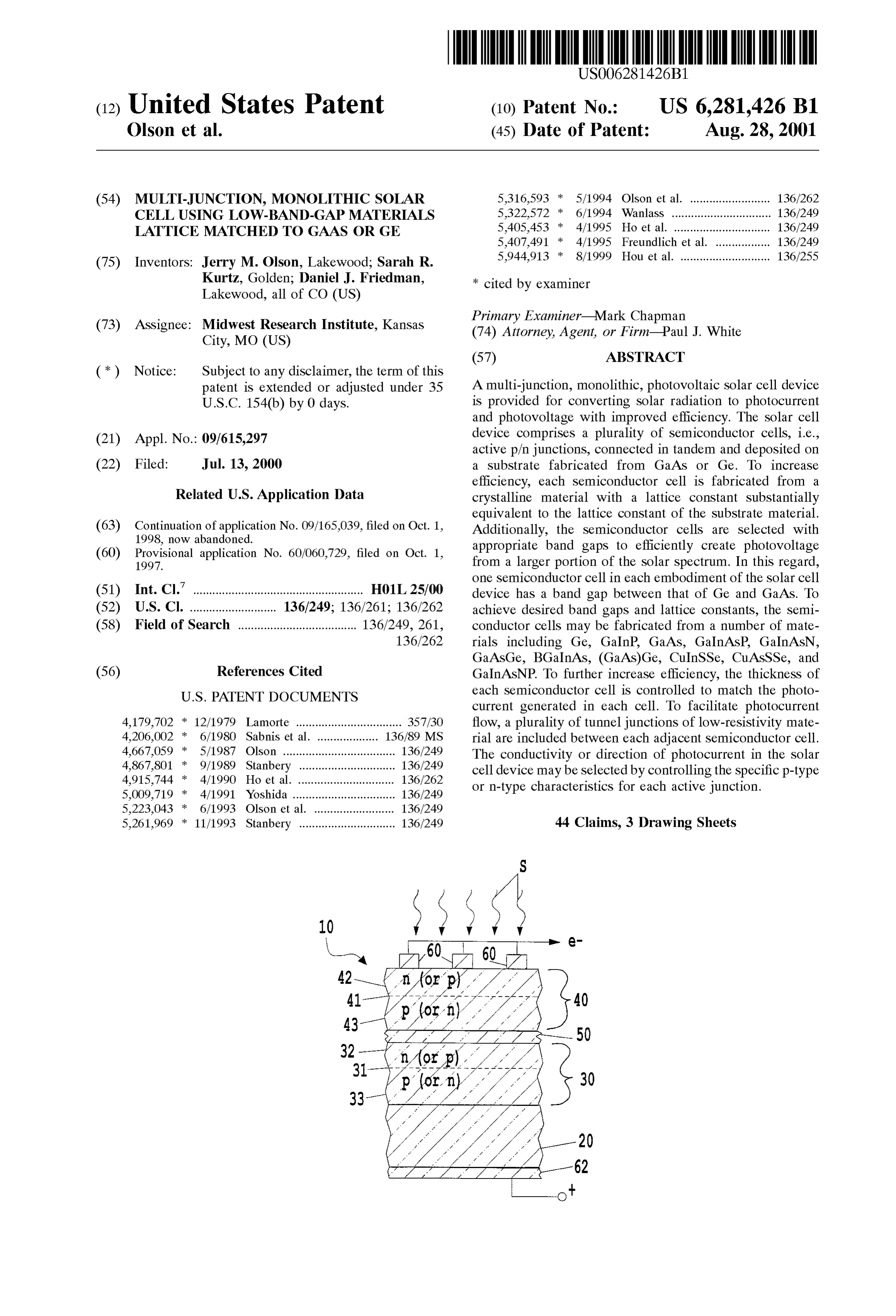
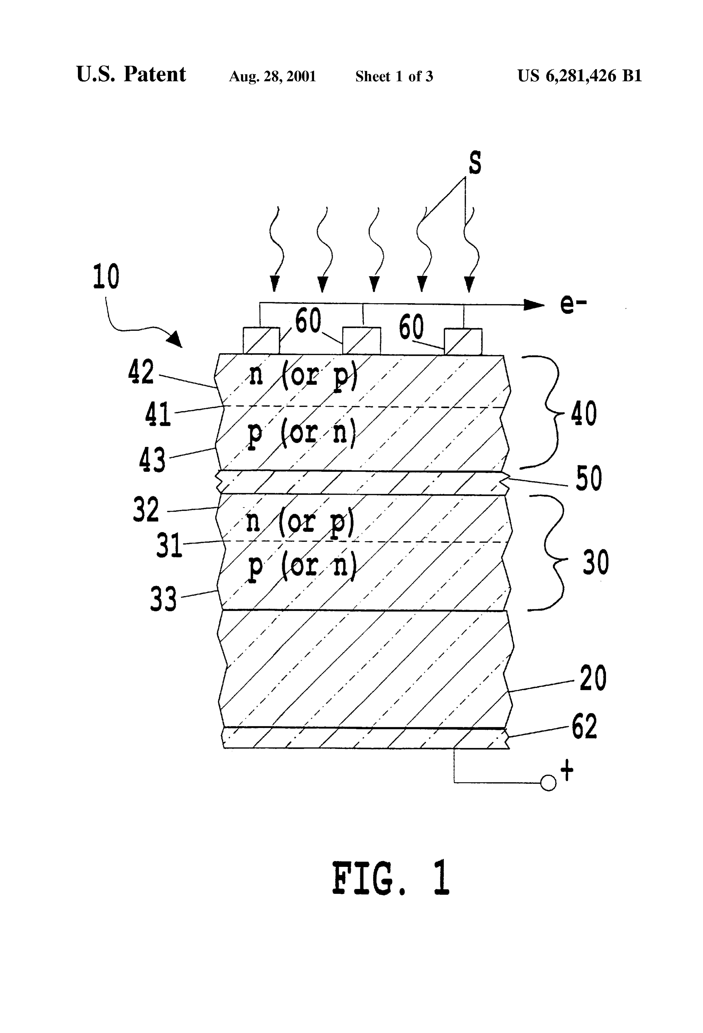
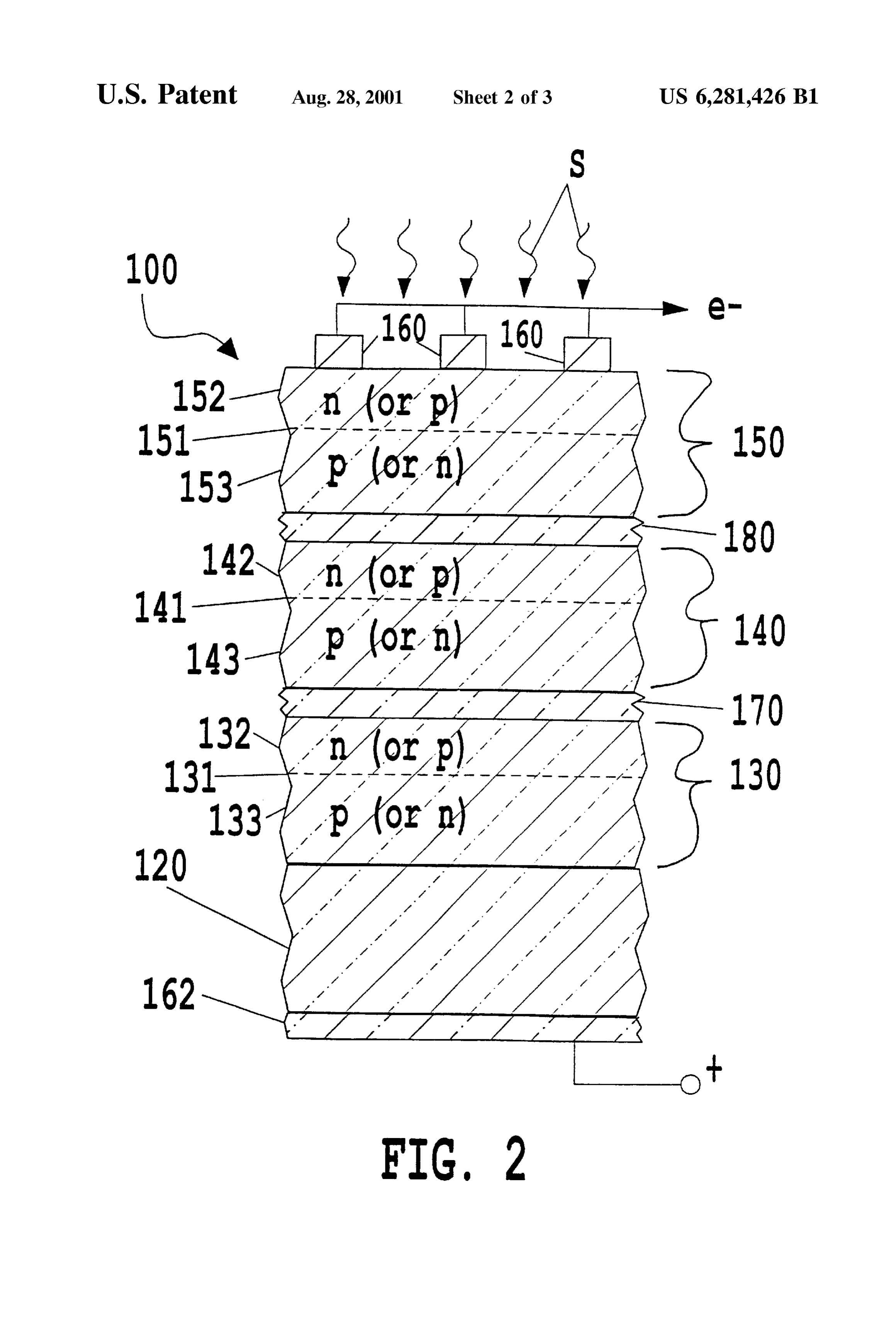
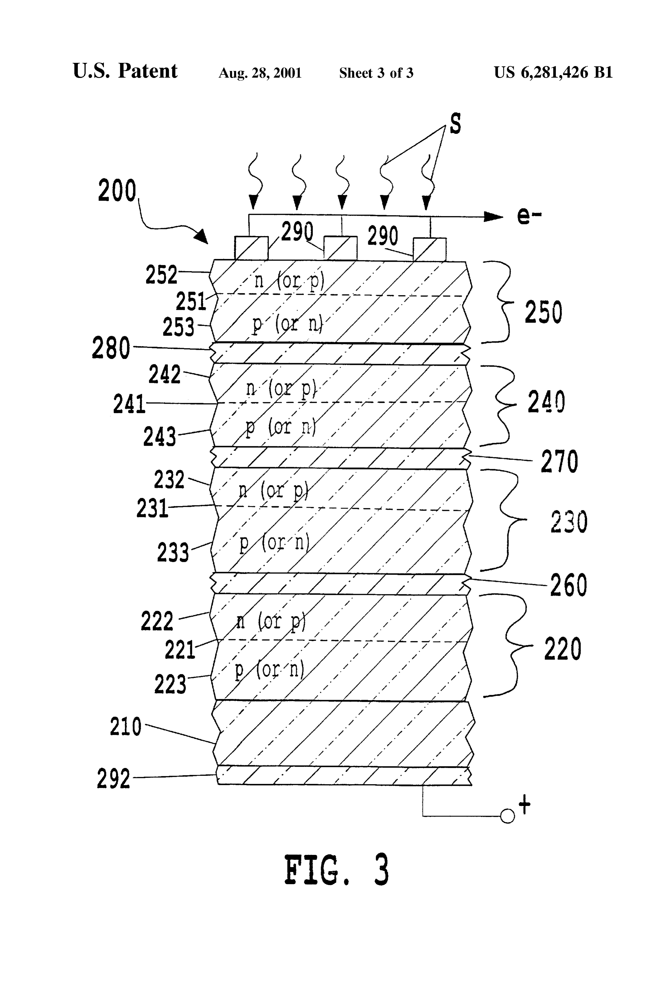
dance with the purposes of the present invention, as embod ied and broadly described herein, each embodiment of the of FIG. a 1 is a Side elevation view in Schematic cross-section multi-junction, monolithic Solar cell of the present multi-junction, monolithic, photovoltaic Solar cell comprises 50 a plurality of Semiconductor cells (i.e., junctions) deposited invention having two active junctions on a Substrate; FIG. 2 is a Side elevation view in Schematic cross-section on a GaAS or Ge Substrate with each Semiconductor cell being fabricated from crystalline materials having Substan of a multi-junction, monolithic Solar cell according to the tially the same lattice constant as the Substrate layer of GaAS present invention having three active junctions on a Sub or Ge and with at least one of the Semiconductor cells having 55 Strate; and a band gap ranging from about 0.67 eV to about 1.4 eV, and FIG. 3 is a Side elevation view in Schematic cross-section preferably about 1 eV. In this manner, the Solar cell of the of a multi-junction, monolithic Solar cell according to the present invention uniquely employs Semiconductor materi present invention having four active junctions on a Substrate. als to more fully capture and convert Solar energy, especially DESCRIPTION OF THE PREFERRED in the 0.67 eV to 1.4 eV energy range which prior to this 60 EMBODIMENT invention had not been efficiently utilized, while facilitating fabrication on a readily available and highly-functional A two-junction Solar cell 10 according to the present GaAS or Ge Substrate. The Solar cell is connected in Series invention is illustrated in Schematic in FIG. 1 with exagger with electrical contacts for applying a load to the Solar cell, ated dimensions and proportions for clarity, as will be and in this regard, the Semiconductor cells are each Substan 65 readily understood by persons skilled in the art. The solar tially current matched for improved photocurrent production cell 10 is a tandem device in which each layer of crystalline by the Solar cell. A tunnel junction is included between each material is epitaxially deposited (i.e., grown) on the previ
Page 7
S 6 ously deposited layer to form the Solar cell 10 from a single provide lattice-matching to a GaAs or Ge substrate 20 while crystal (i.e., monolithic). Persons skilled in the art under providing the above noted energy absorption qualities. Stand that the growth of each layer of crystalline material In another significant feature of the present invention, the attempts to mimic the crystalline structure (i.e., lattice inventors have recognized that desired band gaps and lattice constant) of the initial layer or Substrate, although many matching may be achieved by fabricating the first cell 30 materials are different enough to cause Stresses and mis from a number of Semiconductor materials, including matches at interfaces of Such materials. Such mismatches in Gan 1-ASN 1-, (GaAs) (Ge2)1, B.Gay In 1-AS, lattice constant between the layers of material may result in CuInSSea, and CuASS Sea. The growth process of Significant reductions in the power conversion efficiency of these compounds is preferably controlled Such that the band the Solar cell device 10. In this regard, one of the important gap of the first cell 30 is greater than about 0.67 eV and less aspects of the present invention is the careful Selection of than about 1.3 eV, and more preferably is about 1.0 eV. More materials for each layer of the solar cell device 10 that have particularly, in one preferred embodiment, the first cell is lattice constants which are Substantially equal to that of the Gain, ASN, with x in the range of 0.85 to 0.95 and y Substrate (i.e., lattice-matched materials). In this context, in the range of 0.95 to 0.99 and a band gap of about 1 eV. lattice-matched materials means two materials with lattice 15 The second cell 40 may also be fabricated from a number of constants that are similar enough that when the two mate materials, including Gain-AS,P1, Ga. In-NP, rials are grown adjacent to each other in a Single crystal the AlGaAs, and Ga, In, ASNP. To provide desired difference or mismatch between lattice constants is resolved energy conversion, the growth of the Second cell 40 is by elastic deformation not by inelastic relaxation which controlled to create a band gap in the range of about 1.3 to often results in the formation of dislocations or other unde about 1.8 eV, and more preferably a band gap of about 1.6 sirable defects. eV. Each of these materials or compounds is controllably The Solar cell device 10 generally includes a substrate 20, made to have a lattice constant that is Substantially equiva a first cell 30 with a junction 31, a second cell 40 with a lent to the material (i.e., GaAS or Ge) selected for the junction 41, and a tunnel junction 50. AS Solar radiation, S, Substrate 20. AS may be appreciated, the design of the Solar strikes the Solar cell device 10, the first cell 30 and second 25 cell device 10 facilitates efficient energy conversion for Sun cell 40 each absorbs a portion of the solar radiation, S, and light, S, with energy greater than about 1.0 eV. converts the energy in the form of photons of the Solar An electrical load (not shown) can be connected to the radiation, S, to useable electric energy, measured in photo Solar cell device 10 via grid electrical contacts 60 on top of Voltage and photocurrent. To accomplish this Solar to elec the solar cell device 10 and ohmic plate contact 62 at the tric energy conversion, the first cell 30 and the second cell bottom to facilitate flow of photocurrent e-, o+ through the 40 comprise layers of materials 32, 33 and 42, 43, Solar cell device 10. In other words, the cells 30, 40 are respectively, that are doped (e.g., impurities are added that connected in a Series circuit. AS may be appreciated, the accept or donate electrons) to form n-type and p-type Selection of the direction of conductivity through the Solar Semiconductors. In this manner, the p/n or n/p junctions 31, cell device 10 is controlled by the configuration or polarity 41 are formed in each of the first and second cells 30, 40, 35 of the active junctions 31, 41, and the present invention is respectively. Photons in the received Sun light, S, having expressly applicable to current flow in either direction energy, in eV, greater than the designed band gap of the through the solar cell device 10.
active top cell 40 will be absorbed and converted to elec To facilitate photocurrent flow between cells 30, 40, the tricity across the Semiconductor junction 41 or may pass Solar cell device 10 according to this invention includes a through the active top cell 40 to the next cell 30. Photons 40 low-resistivity tunnel junction layer 50. The tunnel junction with energy less than the designed band gap of the top cell layer 50 may take a number of forms to provide a thin layer 40 will pass through the top cell 40 to the next active cell 30. 50 of materials that allows current to pass between cells 30, Such lower energy Sun light, S, may be absorbed and 40 without generating a voltage drop large enough to Sig converted to electricity acroSS junction 31. To improve nificantly decrease the conversion efficiency of the Solar cell efficient conversion of a fuller range of the Solar spectrum or 45 device 10 and that preserves lattice-matching between the energy, S, to electricity, it is preferable that the lower cell 30 cells 30, 40. For example, the tunnel junction layer 50 may has a band gap that differS Significantly from the band gap be highly doped Semiconductor materials, Such as GaAS. of top cell 40, thereby enabling incremental or stepwise To further facilitate this photocurrent flow and conversion absorption of photons of varying energy levels or wave efficiency of the Solar cell device 10, the first and second lengths. 50 cells 30, 40 may be grown to predetermined thicknesses to In this regard, the illustrated Solar cell device 10 is absorb respective amounts of Solar energy, S, in each cell 30, configured to absorb light in two incremental Steps. In the 40 thus producing matching amounts of photocurrent acroSS top cell 40, photons with energy above about 1.75 eV is each of the junctions 31, 41. This matched current produc absorbed, and photons of energy between about 1.1 eV and tion is important because the cells 30, 40 are stacked, thus 1.75 eV are absorbed in the next cell 30. As shown, the cells 55 connected in Series, which means current flow through the 30, 40 are grown on a crystalline, passivated substrate 20. Solar cell device 10 is limited to the Smallest current flow in A Significant feature of the present invention is the any particular layer of the Solar cell device 10. The current provision of materials that are lattice-matched to the mate flow across each junction 31, 41 is preferably matched in rial of the substrate 20. In this regard, Gallium arsenide each cell 30, 40 at the maximum power level of the Solar cell (GaAs) and germanium (Ge) are desirable base materials for 60 device 10 or at the short-circuit current level, and more monolithic Solar cells for a number of reasons, including the preferably at a point between these levels for improved solar fact that they have Similar lattice constants, Similar thermal energy conversion efficiency. Further, the thicknesses of expansion characteristics, and are generally durable. AS each active cell in the Solar cell device 10 may be selected discussed above, the efficiency of the Solar cell device 10 is to provide optimized Solar energy conversion efficiency at dependent on lattice-matching of each layer of the Solar cell 65 the time the Solar cell device 10 is made and/or for a 10 to the Substrate 20 and to intervening layers. With this in predetermined point in the service life of the solar cell mind, the materials of this invention are Selected carefully to device 10. For example, the thicknesses may be increased or
Page 8
decreased at the time of manufacture to produce a Solar cell compounds Ga, In, ASN, (GaAs),(Ge2), B.Ga, In device 10 with high efficiency for use in a device to be used x-y AS, CuInSSea, and CuASS Sea and with a band gap in Space, Such as a telecommunications Satellite, where injunction 141 greater than about 1.1 eV and less than about Semiconductor materials layerS may degrade. Those perSons 1.3 eV, and more preferably a band gap of about 1.2 eV. skilled in the art will further understand that the conversion More particularly, in one preferred embodiment, cell 140 is efficiency of the Solar cell device 10 may be optimized Gain, ASN, with x in the range of 0.94 to 0.99 and y through a variety of methods, depending on the Semicon in the range of 0.98 to 0.99 and a band gap injunction 141 ductor materials utilized, including Selecting the thicknesses of about 1.2 eV. Cell 130 is preferably fabricated from one of the layers to control cell Voltages and, in Special of the following materials Ge, Ga.In ASN, and circumstances, to mismatch the photocurrent flow (e.g., have (GaAs) (Ge) and with a band gap injunction 131 a larger photocurrent flow in the bottom cell). between about 0.67 eV and 0.9 eV, and more preferably a In contrast to the photocurrent of the Solar cell device 10, band gap of about 0.67 eV.
the photovoltage, which depends on the band gaps of the In a Second embodiment of the three-junction Solar cell cells 30, 40, are additive across the Solar cell device 10. device 100 of the present invention, the band gaps of the Therefore, a plurality of semiconductor cells 30, 40 and 15 junctions 131, 141, and 151 in cells 130, 140, and 150, active junctions 31, 41 of different photovoltages may be respectively, are selected such that junction 151 of cell 150 utilized to convert the Solar radiation, S, received by the absorbs photons with energy greater than about 1.85 eV, Solar cell device 10 to a photovoltage that is cumulative of junction 141 of cell 140 absorbs photons with energies the individual photovoltage levels of the several cells 30, 40. between about 1.4 eV and about 1.85 eV, and junction 131 A three-junction solar cell device 100 according to the of cell 130 absorbs photons with energies between about 1 present invention is illustrated in FIG. 2. From the above eV and about 1.4 eV. An important improvement with this discussion, it may be clear that the use of additional power embodiment is the absorption of photons with energies absorption cells or junctions may improve the efficiency of ranging from about 1 eV to 1.4 eV, thereby facilitating the the solar cell device 100 by providing tighter or smaller production of a larger photovoltage.
incremental absorption of the Solar spectrum, S. The com 25 AS stated above, the materials for each of the cells 130, ponents of the Solar cell device 100 are similar to that of the 140, and 150 are selected and/or produced to have lattice two-junction Solar cell device 10, and include a GaAs or Ge constants substantially equal to that of the substrate 120 Substrate 120, three semiconductor cells 130, 140, and 150 material (i.e., Ge or GaAs). In this regard, cell 150 is with active junctions 131, 141, and 151, respectively, com preferably fabricated from one of the following compounds prising doped Semiconductor material layerS 132, 133, 142, Gaos Inos P, AlGaAS, and AlGaos Inos P with a band 143, and 152, 153, respectively, tunnel junction layers 170 gap in junction 151 in the range of 1.8 eV to 2.0 eV, and and 180 to facilitate photocurrent flow, and front electrical more preferably a band gap of about 1.85 eV. Cell 140 is contacts 160 and back contact 162 to apply a load to the solar preferably fabricated from one of the following compounds cell device 100. As with the two-junction Solar cell device GaAS, Ga, In, ASN, AlGaAs, and Gain-AS,P, 10, the cells 130, 140, and 150 are preferably fabricated 35 with a band gap injunction 141 in the range of 1.3 eV to 1.5 from a material(s) that have lattice constants that are Sub eV, and more preferably a band gap of about 1.4 eV. Cell 130 Stantially equal to that of the material (Ge or GaAS) Selected is preferably fabricated from one of the following materials for the substrate 120 to provide lattice-matching throughout Gan 1-ASN 1-, (GaAs) (Ge2)1, B.Gay In 1-AS, the Solar cell device 100 and improve conversion efficiency. CuInS Sea, and CuASS Sea and with a band gap in Additionally, cells 130, 140, and 150 are current matched by 40 junction 131 between about 0.9 eV and about 1.1 eV, and controlling the thickness, with the final thickness depending more preferably aband gap of about 1 eV. More particularly, upon the Specific material or alloy Selected for each layer. in one preferred embodiment, cell 130 is Ga, In-AS,N- The inventors have recognized that a number of unique with X in the range of 0.85 to 0.95 and y in the range of 0.95 embodiments may be created for a three-junction Solar cell to 0.99 and a band gap in junction 131 of about 1 eV. to meet these requirements and to efficiently absorb an 45 AS recognized by the inventors, the two embodiments of improved portion of the Solar spectrum, S. In one Such the three-junction Solar cells of the present invention, with embodiment of the present invention, the band gaps of the corresponding variations in Semiconductor material, repre cells 130, 140, and 150 are selected such that junction 151 Sent an important improvement over two-junction Solar of cell 150 absorbs photons with energy greater than about cells. These three-junction Solar cells allow a Solar cell to be 1.7 eV, junction 141 of cell 140 absorbs photons with 50 fabricated to convert Solar radiation to electrical energy in energies between about 1.2 eV and about 1.7 eV, and three Steps, with each Step having a Small difference in band junction 131 of cell 130 absorbs photons with energies gaps, or in photon energies absorbed. This incremental between about 0.67 eV and about 1.2 eV. process may be continued with the addition of additional Persons skilled in the art will recognize that this embodi active junctions that provide one additional Step for con ment provides an important improvement by enabling the 55 Verting the received Solar radiation. Again, the Solar cell is absorption of photons with energies ranging from about 0.67 preferably fabricated to be lattice- and current-matched. eV to 1.7 eV in two steps rather than one step, thereby In another Significant feature of the present invention, a facilitating the production of a larger photovoltage. Further, four-junction, monolithic Solar cell device 200 of the present the materials for each of the cells 130, 140, and 150 are invention which absorbs Solar radiation in four StepS is Selected and/or produced to have lattice constants Substan 60 illustrated in FIG. 3. A variety of semiconductor materials tially equal to that of the substrate 120 material (i.e., Ge or and Substrates may be utilized to fabricate four-junction cell GaAs). In this regard, cell 150 is preferably fabricated from device 200 with the added (fourth) junction being selected to one of the following compounds Ga, In, ASP have a band gap that better facilitates absorption of the Solar Ga, In-NP, AlGaAs, and Ga, In-AS,N-P--- 65 spectrum. For example, Solar cell device 200 may be with junction 151 having a band gap in the range of 1.6 to designed with a junction having a band gap lower, 1.9 eV, and more preferably a band gap of about 1.7 eV. Cell intermediate, or higher than in a three-junction cell to 140 is preferably fabricated from one of the following improve the Solar to electric energy conversion of a three
Page 9
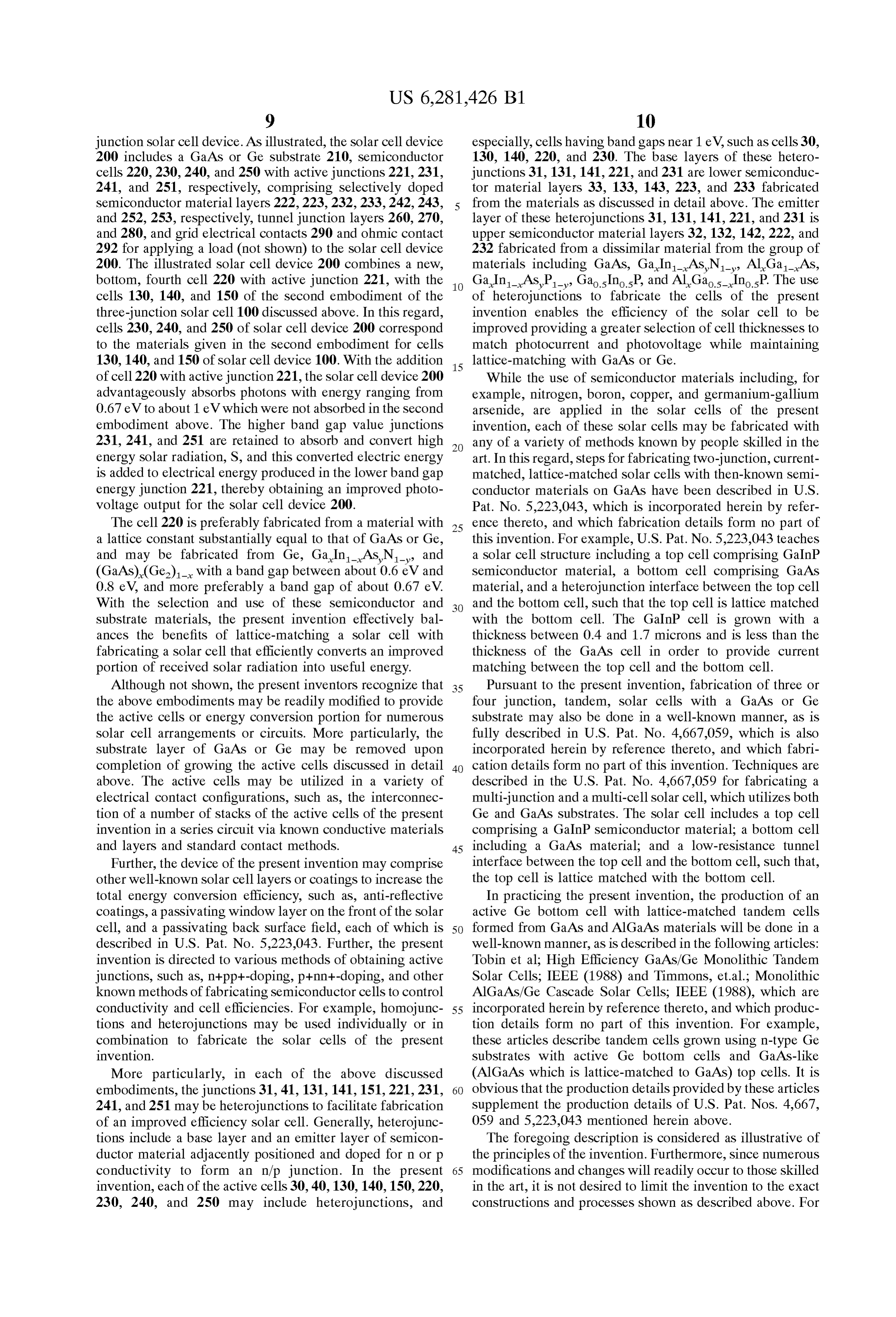
junction Solar cell device. AS illustrated, the Solar cell device especially, cells having band gaps near 1 eV, Such as cells 30, 200 includes a GaAS or Ge Substrate 210, semiconductor 130, 140, 220, and 230. The base layers of these hetero cells 220, 230, 240, and 250 with active junctions 221, 231, junctions 31, 131, 141, 221, and 231 are lower semiconduc 241, and 251, respectively, comprising Selectively doped tor material layers 33, 133, 143, 223, and 233 fabricated semiconductor material layers 222, 223, 232,233,242, 243, from the materials as discussed in detail above. The emitter and 252,253, respectively, tunnel junction layers 260, 270, layer of these heterojunctions 31, 131, 141, 221, and 231 is and 280, and grid electrical contacts 290 and ohmic contact upper Semiconductor material layerS 32, 132, 142,222, and 292 for applying a load (not shown) to the solar cell device 232 fabricated from a dissimilar material from the group of 200. The illustrated Solar cell device 200 combines a new, materials including GaAS, Ga. In 1-AS, N, AlGaAS, bottom, fourth cell 220 with active junction 221, with the Gain, ASP, Gaos InosP, and AlGaos Inos P. The use cells 130, 140, and 150 of the second embodiment of the of heterojunctions to fabricate the cells of the present three-junction solar cell 100 discussed above. In this regard, invention enables the efficiency of the solar cell to be cells 230, 240, and 250 of solar cell device 200 correspond improved providing a greater Selection of cell thicknesses to to the materials given in the Second embodiment for cells match photocurrent and photovoltage while maintaining 130, 140, and 150 of Solar cell device 100. With the addition 15 lattice-matching with GaAS or Ge. of cell 220 with active junction 221, the Solar cell device 200 While the use of semiconductor materials including, for advantageously absorbs photons with energy ranging from example, nitrogen, boron, copper, and germanium-gallium 0.67 eV to about 1 eV which were not absorbed in the second arsenide, are applied in the Solar cells of the present embodiment above. The higher band gap value junctions invention, each of these solar cells may be fabricated with 231, 241, and 251 are retained to absorb and convert high any of a variety of methods known by people skilled in the energy Solar radiation, S, and this converted electric energy art. In this regard, Steps for fabricating two-junction, current is added to electrical energy produced in the lower band gap matched, lattice-matched Solar cells with then-known Semi energy junction 221, thereby obtaining an improved photo conductor materials on GaAs have been described in U.S. voltage output for the solar cell device 200. Pat. No. 5,223,043, which is incorporated herein by refer The cell 220 is preferably fabricated from a material with 25 ence thereto, and which fabrication details form no part of a lattice constant Substantially equal to that of GaAS or Ge, this invention. For example, U.S. Pat. No. 5,223,043 teaches and may be fabricated from Ge, Ga, In, ASN, and a Solar cell Structure including a top cell comprising Ganp (GaAs) (Ge) with a band gap between about 0.6 eV and Semiconductor material, a bottom cell comprising GaAS 0.8 eV, and more preferably a band gap of about 0.67 eV. material, and a heterojunction interface between the top cell With the selection and use of these semiconductor and and the bottom cell, Such that the top cell is lattice matched Substrate materials, the present invention effectively bal with the bottom cell. The GalnP cell is grown with a ances the benefits of lattice-matching a Solar cell with thickness between 0.4 and 1.7 microns and is less than the fabricating a Solar cell that efficiently converts an improved thickness of the GaAS cell in order to provide current portion of received Solar radiation into useful energy. matching between the top cell and the bottom cell. Although not shown, the present inventors recognize that 35 Pursuant to the present invention, fabrication of three or the above embodiments may be readily modified to provide four junction, tandem, Solar cells with a GaAS or Ge the active cells or energy conversion portion for numerous Substrate may also be done in a well-known manner, as is Solar cell arrangements or circuits. More particularly, the fully described in U.S. Pat. No. 4,667,059, which is also Substrate layer of GaAS or Ge may be removed upon incorporated herein by reference thereto, and which fabri completion of growing the active cells discussed in detail 40 cation details form no part of this invention. Techniques are above. The active cells may be utilized in a variety of described in the U.S. Pat. No. 4,667,059 for fabricating a electrical contact configurations, Such as, the interconnec multi-junction and a multi-cell Solar cell, which utilizes both tion of a number of Stacks of the active cells of the present Ge and GaAS Substrates. The Solar cell includes a top cell invention in a Series circuit via known conductive materials comprising a Ganp Semiconductor material; a bottom cell and layerS and Standard contact methods. 45 including a GaAS material; and a low-resistance tunnel Further, the device of the present invention may comprise interface between the top cell and the bottom cell, Such that, other well-known Solar cell layerS or coatings to increase the the top cell is lattice matched with the bottom cell. total energy conversion efficiency, Such as, anti-reflective In practicing the present invention, the production of an coatings, a passivating window layer on the front of the Solar active Ge bottom cell with lattice-matched tandem cells cell, and a passivating back Surface field, each of which is 50 formed from GaAS and AlGaAS materials will be done in a described in U.S. Pat. No. 5,223,043. Further, the present well-known manner, as is described in the following articles: invention is directed to various methods of obtaining active Tobin et al; High Efficiency GaAs/Ge Monolithic Tandem junctions, Such as, n+pp+-doping, p+nn+-doping, and other Solar Cells; IEEE (1988) and Timmons, et al.; Monolithic known methods of fabricating Semiconductor cells to control AlGaAs/Ge Cascade Solar Cells; IEEE (1988), which are conductivity and cell efficiencies. For example, homojunc 55 incorporated herein by reference thereto, and which produc tions and heterojunctions may be used individually or in tion details form no part of this invention. For example, combination to fabricate the Solar cells of the present these articles describe tandem cells grown using n-type Ge invention. Substrates with active Ge bottom cells and GaAS-like More particularly, in each of the above discussed (AlGaAs which is lattice-matched to GaAs) top cells. It is embodiments, the junctions 31, 41,131, 141, 151, 221, 231, 60 obvious that the production details provided by these articles 241, and 251 may be heterojunctions to facilitate fabrication supplement the production details of U.S. Pat. Nos. 4,667, of an improved efficiency Solar cell. Generally, heterojunc 059 and 5,223,043 mentioned herein above. tions include a base layer and an emitter layer of Semicon The foregoing description is considered as illustrative of ductor material adjacently positioned and doped for n or p the principles of the invention. Furthermore, Since numerous conductivity to form an n/p junction. In the present 65 modifications and changes will readily occur to those skilled invention, each of the active cells 30, 40,130, 140,150, 220, in the art, it is not desired to limit the invention to the exact 230, 240, and 250 may include heterojunctions, and constructions and processes shown as described above. For
Page 10
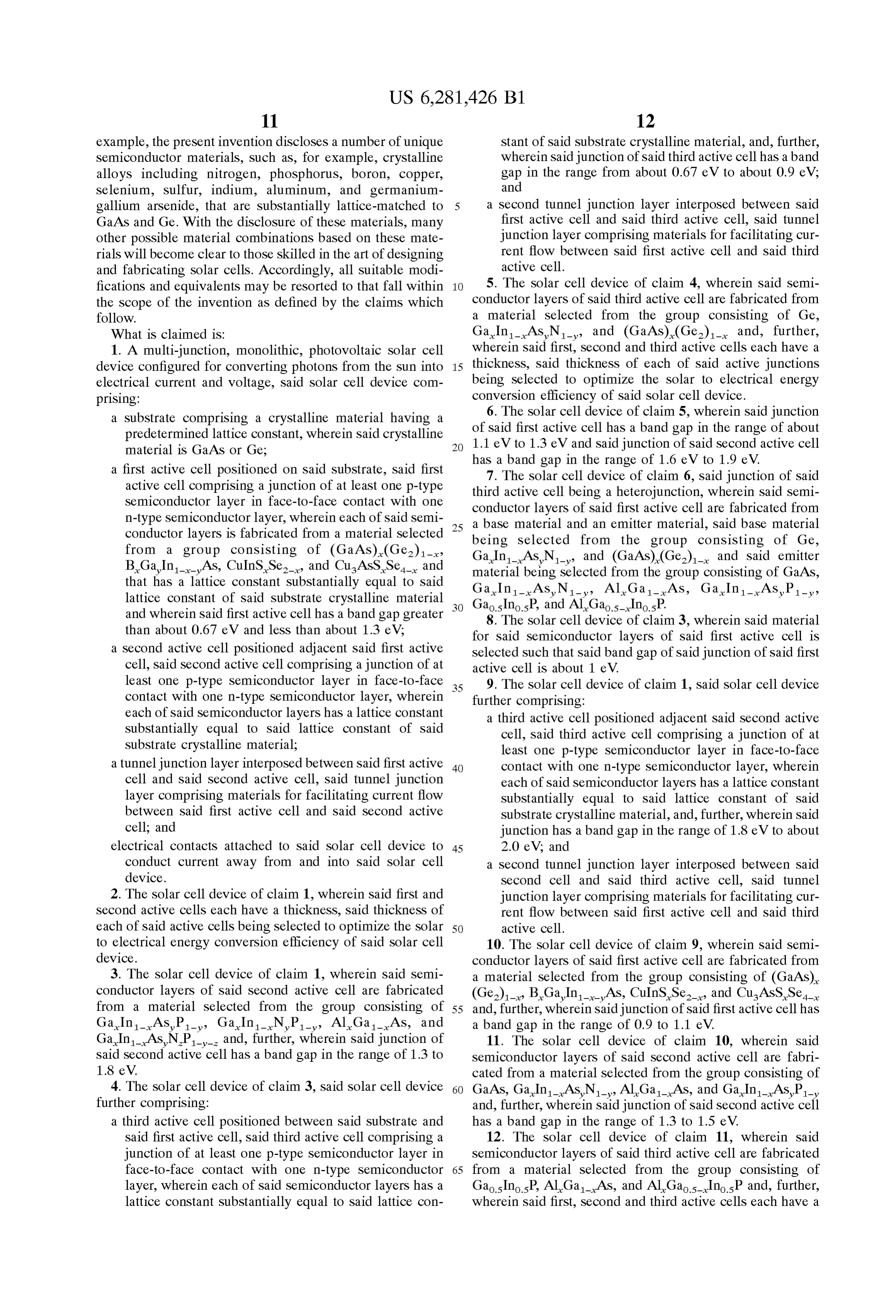
example, the present invention discloses a number of unique Stant of Said Substrate crystalline material, and, further, Semiconductor materials, Such as, for example, crystalline wherein Said junction of Said third active cell has a band alloys including nitrogen, phosphorus, boron, copper, gap in the range from about 0.67 eV to about 0.9 eV; Selenium, Sulfur, indium, aluminum, and germanium and gallium arsenide, that are Substantially lattice-matched to 5 a Second tunnel junction layer interposed between Said GaAs and Ge. With the disclosure of these materials, many first active cell and Said third active cell, Said tunnel other possible material combinations based on these mate junction layer comprising materials for facilitating cur rials will become clear to those skilled in the art of designing rent flow between said first active cell and said third and fabricating Solar cells. Accordingly, all Suitable modi active cell.
fications and equivalents may be resorted to that fall within 5. The Solar cell device of claim 4, wherein said semi the scope of the invention as defined by the claims which conductor layers of said third active cell are fabricated from follow. a material Selected from the group consisting of Ge, What is claimed is: Ga, In-AS,N-, and (GaAs), (Ge2), and, further, 1. A multi-junction, monolithic, photovoltaic Solar cell wherein Said first, Second and third active cells each have a device configured for converting photons from the Sun into 15 thickness, Said thickness of each of Said active junctions electrical current and Voltage, Said Solar cell device com being Selected to optimize the Solar to electrical energy prising: conversion efficiency of Said Solar cell device. a Substrate comprising a crystalline material having a 6. The Solar cell device of claim 5, wherein said junction predetermined lattice constant, wherein Said crystalline of Said first active cell has a band gap in the range of about material is GaAS or Ge; 1.1 eV to 1.3 eV and said junction of said second active cell a first active cell positioned on Said Substrate, Said first has7.aThe band gap in the range of 1.6 eV to 1.9 eV.
active cell comprising a junction of at least one p-type third activesolar cell device of claim 6, said junction of said cell being a heterojunction, wherein Said Semi
Semiconductor layer in face-to-face contact with one conductor layers of Said first active cell are fabricated from n-type Semiconductor layer, wherein each of Said Semi 25 a base material and an emitter material, Said base material conductor layerS is fabricated from a material Selected being Selected from the group consisting of Ge, from a group consisting of (GaAs) (Ge2), Gain, ASN, and (GaAs),(Ge2), and said emitter BGa, In, AS, CuInS,Sea, and CusASS...Sea and material being Selected from the group consisting of GaAS, that has a lattice constant Substantially equal to Said Ga, In 1-AS,N1, AlGaAs, Ga. In 1-ASP lattice constant of Said Substrate crystalline material Gaos Inos P, and AlGaos. Inos P.
and wherein Said first active cell has a band gap greater 8. The Solar cell device of claim 3, wherein said material than about 0.67 eV and less than about 1.3 eV. for Said Semiconductor layers of Said first active cell is a Second active cell positioned adjacent Said first active Selected Such that said band gap of Said junction of Said first cell, Said Second active cell comprising a junction of at active cell is about 1 eV.
least one p-type Semiconductor layer in face-to-face 35 9. The Solar cell device of claim 1, said Solar cell device contact with one n-type Semiconductor layer, wherein further comprising:
each of Said Semiconductor layerS has a lattice constant a third active cell positioned adjacent Said Second active Substantially equal to Said lattice constant of Said cell, Said third active cell comprising a junction of at Substrate crystalline material; least one p-type Semiconductor layer in face-to-face a tunnel junction layer interposed between said first active 40 contact with one n-type Semiconductor layer, wherein cell and Said Second active cell, Said tunnel junction each of Said Semiconductor layerS has a lattice constant layer comprising materials for facilitating current flow Substantially equal to Said lattice constant of Said between Said first active cell and Said Second active Substrate crystalline material, and, further, wherein Said cell; and junction has a band gap in the range of 1.8 eV to about electrical contacts attached to Said Solar cell device to 45 2.0 eV; and conduct current away from and into Said Solar cell a Second tunnel junction layer interposed between Said device. Second cell and Said third active cell, Said tunnel 2. The Solar cell device of claim 1, wherein said first and junction layer comprising materials for facilitating cur Second active cells each have a thickness, Said thickness of rent flow between said first active cell and said third each of Said active cells being Selected to optimize the Solar 50 active cell.
to electrical energy conversion efficiency of Said Solar cell 10. The Solar cell device of claim 9, wherein said semi device. conductor layers of Said first active cell are fabricated from 3. The Solar cell device of claim 1, wherein said semi a material Selected from the group consisting of (GaAs), conductor layers of Said Second active cell are fabricated (Ge2), B,Ga, In, AS, CuInS,Sea, and CusASS...Sea. from a material Selected from the group consisting of 55 and, further, wherein Saidjunction of Said first active cell has Ga.In 1-AS,P, Ga. In-NP, AlGaAs, and a band gap in the range of 0.9 to 1.1 eV.
Ga, In, ASNP, and, further, wherein said junction of 11. The Solar cell device of claim 10, wherein said Said Second active cell has a band gap in the range of 1.3 to Semiconductor layers of Said Second active cell are fabri 18 eV. cated from a material Selected from the group consisting of 4. The Solar cell device of claim 3, said Solar cell device 60 GaAS, Ga. In 1-AS, N, AlGaAs, and Gain-AS,Pfurther comprising: and, further, wherein Said junction of Said Second active cell a third active cell positioned between Said Substrate and has a band gap in the range of 1.3 to 1.5 eV. Said first active cell, Said third active cell comprising a 12. The Solar cell device of claim 11, wherein said junction of at least one p-type Semiconductor layer in Semiconductor layers of Said third active cell are fabricated face-to-face contact with one n-type Semiconductor 65 from a material Selected from the group consisting of layer, wherein each of Said Semiconductor layerS has a Gaos Inos P, AlGaAS, and AlGaos Inos P and, further, lattice constant Substantially equal to Said lattice con wherein Said first, Second and third active cells each have a
Page 11
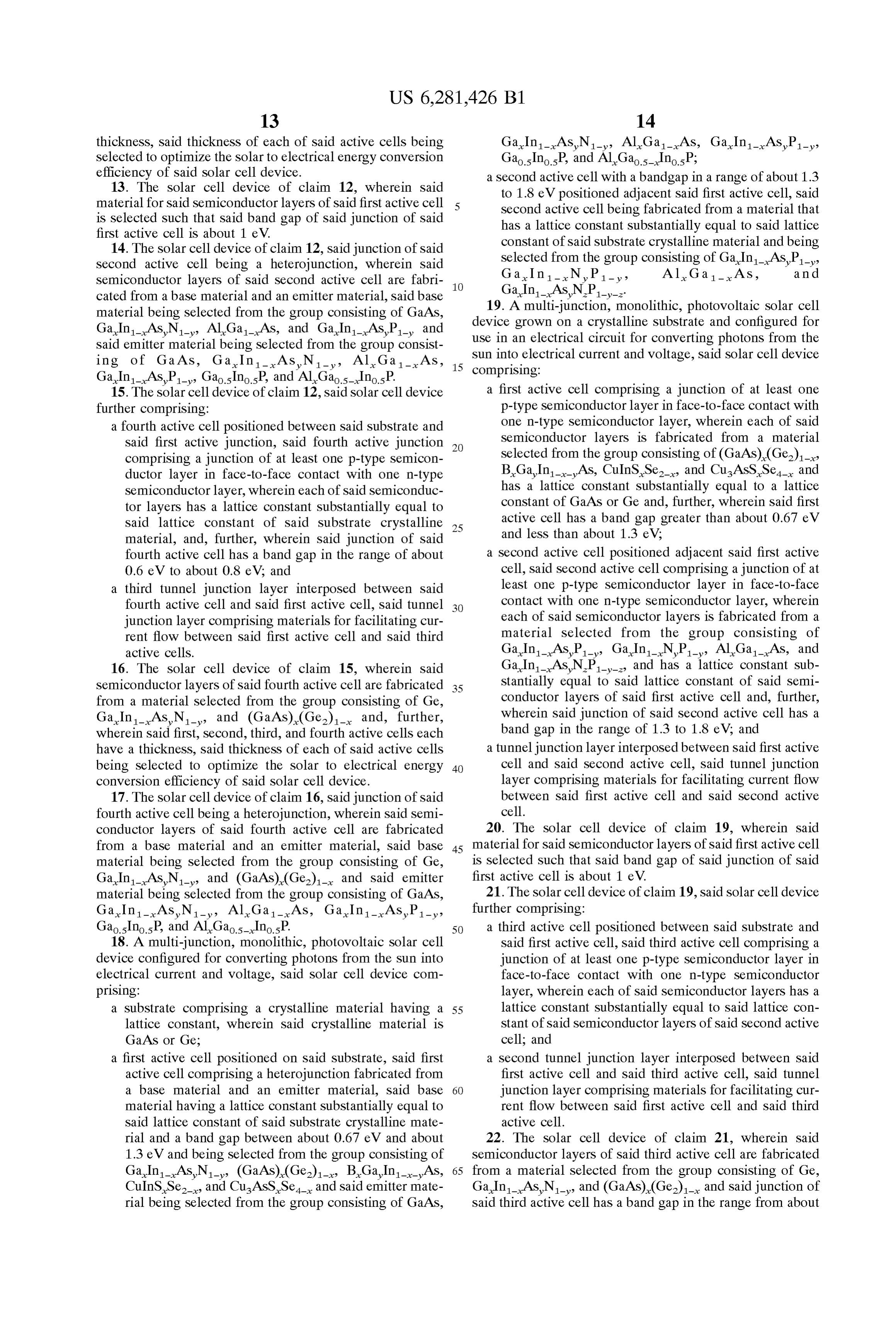
thickness, Said thickness of each of Said active cells being Ga, In 1-AS,N1, AlGaAs, Ga.In 1-ASP 1-y Selected to optimize the Solar to electrical energy conversion Gaos Inos P, and AlGaos. Inos P. efficiency of Said Solar cell device. a Second active cell with a bandgap in a range of about 1.3 13. The Solar cell device of claim 12, wherein said to 1.8 eV positioned adjacent Said first active cell, Said material for Said Semiconductor layers of Said first active cell Second active cell being fabricated from a material that is Selected Such that Said band gap of Said junction of Said has a lattice constant Substantially equal to Said lattice first active cell is about 1 eV.
14. The Solar cell device of claim 12, said junction of said constant of Said Substrate crystalline material and being Second active cell being a heterojunction, wherein Said Selected from the group consisting of Gain-ASP1-y
Semiconductor layers of Said Second active cell are fabri cated from a base material and an emitter material, Said base Ga, In, AS, NP---.
material being Selected from the group consisting of GaAS, 19. A multi-junction, monolithic, photovoltaic Solar cell device grown on a crystalline Substrate and configured for
Ga, In, ASN, AlGaAS, and Ga, In, ASP, and
Said emitter material being Selected from the group consist use Sun in an electrical circuit for converting photons from the into electrical current and Voltage, Said Solar cell device ing of Ga AS, Ga. In ASN, AlGaAs, 15 comprising:
Gan 1-ASP1, Gaos Inos P, and AlGaos. Inos P. a first active cell comprising a junction of at least one 15. The Solar cell device of claim 12, said Solar cell device further comprising: p-type Semiconductor layer in face-to-face contact with a fourth active cell positioned between Said Substrate and one n-type Semiconductor layer, wherein each of Said Said first active junction, Said fourth active junction Semiconductor layerS is fabricated from a material comprising a junction of at least one p-type Semicon Selected from the group consisting of (GaAs) (Ge), ductor layer in face-to-face contact with one n-type B,Ga, In, AS, CuInS,Sea, and CusASS...Sea and Semiconductor layer, wherein each of Said Semiconduc has a lattice constant Substantially equal to a lattice tor layerS has a lattice constant Substantially equal to constant of GaAS or Ge and, further, wherein Said first Said lattice constant of Said Substrate crystalline 25 active cell has a band gap greater than about 0.67 eV material, and, further, wherein Said junction of Said and less than about 1.3 eV.
fourth active cell has a band gap in the range of about a Second active cell positioned adjacent Said first active 0.6 eV to about 0.8 eV; and cell, Said Second active cell comprising a junction of at a third tunnel junction layer interposed between said least one p-type Semiconductor layer in face-to-face fourth active cell and Said first active cell, Said tunnel contact with one n-type Semiconductor layer, wherein junction layer comprising materials for facilitating cur each of Said Semiconductor layerS is fabricated from a rent flow between said first active cell and said third material Selected from the group consisting of active cells. Ga, In, ASP, Ga. In-NP, AlGaAs, and 16. The Solar cell device of claim 15, wherein said Gain, ASNP, and has a lattice constant Sub Semiconductor layers of Said fourth active cell are fabricated 35 Stantially equal to Said lattice constant of Said Semi from a material Selected from the group consisting of Ge, conductor layers of Said first active cell and, further, Ga.In 1-AS,N-, and (GaAs), (Ge2), and, further, wherein Said junction of Said Second active cell has a wherein Said first, Second, third, and fourth active cells each band gap in the range of 1.3 to 1.8 eV; and have a thickness, Said thickness of each of Said active cells a tunnel junction layer interposed between Said first active being Selected to optimize the Solar to electrical energy 40 cell and Said Second active cell, Said tunnel junction conversion efficiency of Said Solar cell device. layer comprising materials for facilitating current flow 17. The Solar cell device of claim 16, said junction of said between Said first active cell and Said Second active fourth active cell being a heterojunction, wherein Said Semi cell.
conductor layers of Said fourth active cell are fabricated 20. The Solar cell device of claim 19, wherein said from a base material and an emitter material, Said base 45 material for Said Semiconductor layers of Said first active cell material being Selected from the group consisting of Ge, is Selected Such that Said band gap of Said junction of Said Ga, In, ASN, and (GaAs),(Ge2), and Said emitter first active cell is about 1 eV. material being Selected from the group consisting of GaAS, 21. The Solar cell device of claim 19, said Solar cell device Ga, In, ASN 1-, AlGaAs, Ga. In 1-ASP further comprising:
Gaos Inos P, and AlGaos. Inos P. 50 a third active cell positioned between Said Substrate and 18. A multi-junction, monolithic, photovoltaic Solar cell Said first active cell, Said third active cell comprising a device configured for converting photons from the Sun into junction of at least one p-type Semiconductor layer in electrical current and Voltage, Said Solar cell device com face-to-face contact with one n-type Semiconductor prising: layer, wherein each of Said Semiconductor layerS has a a Substrate comprising a crystalline material having a 55 lattice constant Substantially equal to Said lattice con lattice constant, wherein Said crystalline material is Stant of Said Semiconductor layers of Said Second active GaAS or Ge; cell; and a first active cell positioned on Said Substrate, Said first a Second tunnel junction layer interposed between Said active cell comprising a heterojunction fabricated from first active cell and Said third active cell, Said tunnel a base material and an emitter material, Said base 60 junction layer comprising materials for facilitating cur material having a lattice constant Substantially equal to rent flow between said first active cell and said third Said lattice constant of Said Substrate crystalline mate active cell.
rial and a band gap between about 0.67 eV and about 22. The Solar cell device of claim 21, wherein said 1.3 eV and being Selected from the group consisting of Semiconductor layers of Said third active cell are fabricated Gan 1-ASN1, (GaAs),(Ge2), B.Gan 1-AS, 65 from a material Selected from the group consisting of Ge,
CuInSSea, and CuASS Sea and Said emitter mate Gan-AS,N-, and (GaAs),(Ge2), and Said junction of rial being Selected from the group consisting of GaAS, Said third active cell has a band gap in the range from about
Page 12
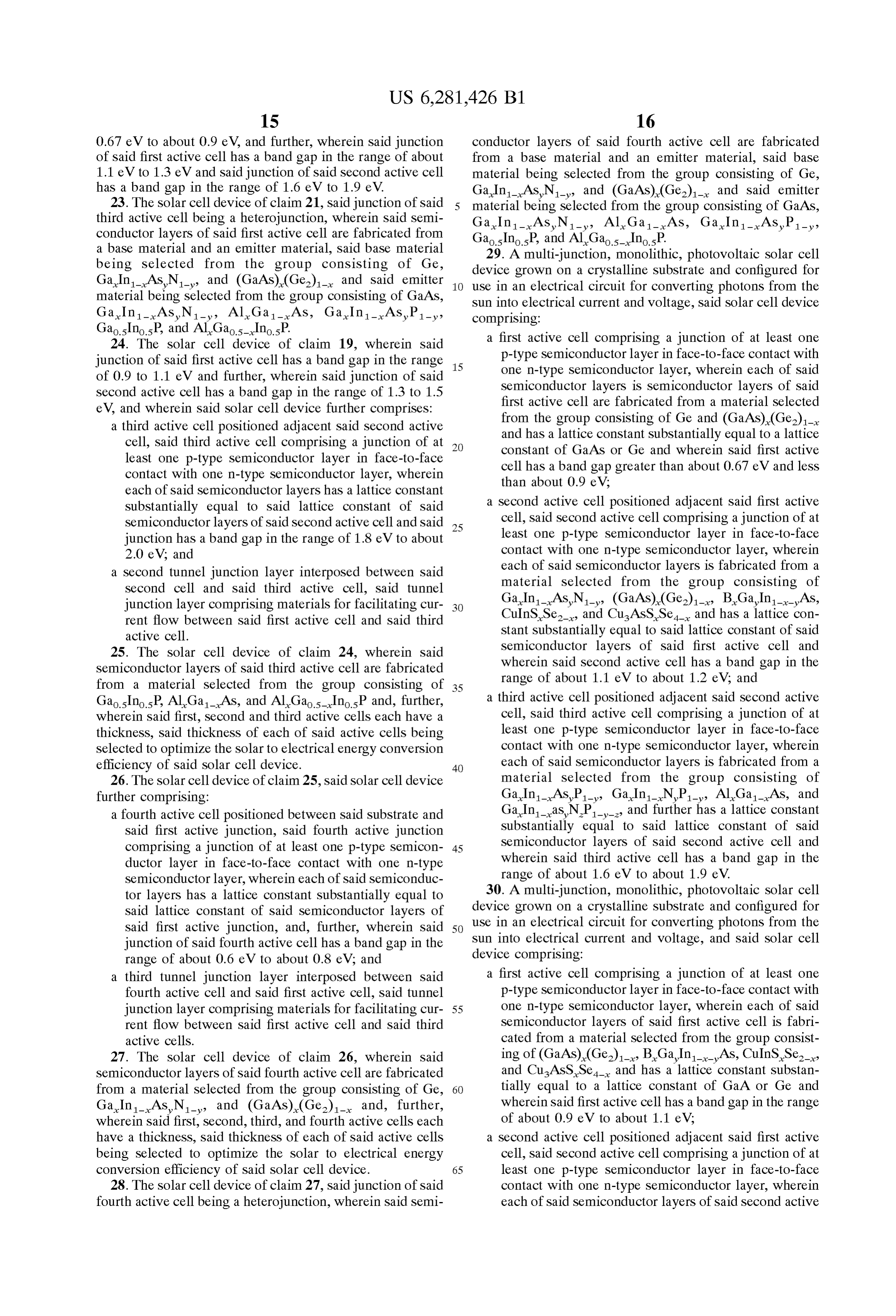
0.67 eV to about 0.9 eV, and further, wherein said junction conductor layers of Said fourth active cell are fabricated of Said first active cell has a band gap in the range of about from a base material and an emitter material, Said base 1.1 eV to 1.3 eV and said junction of said second active cell material being Selected from the group consisting of Ge, has a band gap in the range of 1.6 eV to 1.9 eV. Gan-AS,N-, and (GaAs),(Ge2), and Said emitter 23. The solar cell device of claim 21, said junction of said material being Selected from the group consisting of GaAS, third active cell being a heterojunction, wherein Said Semi Ga, In, ASN 1-, AlGaAs, Ga. In 1-ASP 1-y conductor layers of Said first active cell are fabricated from Gaos Inos P, and AlGaos. Inos P. a base material and an emitter material, Said base material 29. A multi-junction, monolithic, photovoltaic Solar cell being Selected from the group consisting of Ge, device grown on a crystalline Substrate and configured for Ga, In, ASN, and (GaAs),(Ge2), and said emitter material being Selected from the group consisting of GaAS, use in an electrical circuit for converting photons from the Sun into electrical current and Voltage, Said Solar cell device
Ga, In, ASN 1-, AlGaAs, Ga. In 1-ASP comprising:
Gaos Inos P, and AlGaos. Inos P. a first active cell comprising a junction of at least one 24. The Solar cell device of claim 19, wherein said junction of Said first active cell has a band gap in the range 15 p-type Semiconductor layer in face-to-face contact with of 0.9 to 1.1 eV and further, wherein said junction of said one n-type Semiconductor layer, wherein each of Said Second active cell has a band gap in the range of 1.3 to 1.5 Semiconductor layerS is Semiconductor layers of Said first active cell are fabricated from a material Selected eV, and wherein Said Solar cell device further comprises: from the group consisting of Ge and (GaAS) (Ge). a third active cell positioned adjacent Said Second active and has a lattice constant Substantially equal to a lattice cell, Said third active cell comprising a junction of at constant of GaAS or Ge and wherein Said first active least one p-type Semiconductor layer in face-to-face cell has a band gap greater than about 0.67 eV and leSS contact with one n-type Semiconductor layer, wherein than about 0.9 eV;
each of Said Semiconductor layerS has a lattice constant
Substantially equal to Said lattice constant of Said a Second active cell positioned adjacent Said first active Semiconductor layers of Said Second active cell and Said 25 cell, Said Second active cell comprising a junction of at junction has a band gap in the range of 1.8 eV to about least one p-type Semiconductor layer in face-to-face 2.0 eV; and contact with one n-type Semiconductor layer, wherein a Second tunnel junction layer interposed between said each of Said Semiconductor layerS is fabricated from a Second cell and Said third active cell, Said tunnel material Selected from the group consisting of junction layer comprising materials for facilitating cur Gan 1-ASN1, (GaAs),(Ge2), B.Gan 1-AS, rent flow between said first active cell and said third CuInSSea, and CuASS Sea and has a lattice con active cell. Stant Substantially equal to Said lattice constant of Said 25. The Solar cell device of claim 24, wherein said Semiconductor layers of Said first active cell and Semiconductor layers of Said third active cell are fabricated wherein said Second active cell has a band gap in the from a material Selected from the group consisting of 35 range of about 1.1 eV to about 1.2 eV; and Gaos Inos P, AlGaAS, and AlGaos. Inos P and, further, a third active cell positioned adjacent Said Second active wherein Said first, Second and third active cells each have a cell, Said third active cell comprising a junction of at thickness, Said thickness of each of Said active cells being least one p-type Semiconductor layer in face-to-face Selected to optimize the Solar to electrical energy conversion contact with one n-type Semiconductor layer, wherein efficiency of Said Solar cell device. 40 each of Said Semiconductor layerS is fabricated from a 26. The Solar cell device of claim 25, said Solar cell device material Selected from the group consisting of further comprising: Ga, In, ASP, Ga. In-NP, AlGaAS, and a fourth active cell positioned between Said Substrate and Gainas, N.P., and further has a lattice constant Said first active junction, Said fourth active junction Substantially equal to Said lattice constant of Said comprising a junction of at least one p-type Semicon 45 Semiconductor layers of Said Second active cell and ductor layer in face-to-face contact with one n-type wherein Said third active cell has a band gap in the Semiconductor layer, wherein each of Said Semiconduc range of about 1.6 eV to about 1.9 eV. tor layerS has a lattice constant Substantially equal to 30. A multi-junction, monolithic, photovoltaic Solar cell Said lattice constant of Said Semiconductor layers of device grown on a crystalline Substrate and configured for Said first active junction, and, further, wherein Said 50 use in an electrical circuit for converting photons from the junction of Said fourth active cell has a band gap in the Sun into electrical current and Voltage, and Said Solar cell range of about 0.6 eV to about 0.8 eV; and device comprising:
a third tunnel junction layer interposed between said a first active cell comprising a junction of at least one fourth active cell and Said first active cell, Said tunnel p-type Semiconductor layer in face-to-face contact with junction layer comprising materials for facilitating cur 55 one n-type Semiconductor layer, wherein each of Said rent flow between said first active cell and said third Semiconductor layers of Said first active cell is fabri active cells. cated from a material Selected from the group consist 27. The Solar cell device of claim 26, wherein said ing of (GaAs),(Ge2), B,Ga, In, AS, CuInS,Sea, Semiconductor layers of Said fourth active cell are fabricated and CuASS Sea and has a lattice constant Substan from a material Selected from the group consisting of Ge, 60 tially equal to a lattice constant of GaA. or Ge and Ga.In 1-AS,N-, and (GaAs), (Ge2), and, further, wherein Said first active cell has a band gap in the range wherein Said first, Second, third, and fourth active cells each of about 0.9 eV to about 1.1 eV; have a thickness, Said thickness of each of Said active cells a Second active cell positioned adjacent Said first active being Selected to optimize the Solar to electrical energy cell, Said Second active cell comprising a junction of at conversion efficiency of Said Solar cell device. 65 least one p-type Semiconductor layer in face-to-face 28. The solar cell device of claim 27, said junction of said contact with one n-type Semiconductor layer, wherein fourth active cell being a heterojunction, wherein Said Semi each of Said Semiconductor layers of Said Second active
Page 13
cell is fabricated from a material selected from the Gaos Inos P, and AlGaos Inos P, and further wherein group consisting of GaAs, Ga. In ASN, each of Said base and emitter materials has a lattice AlGaAs, and Ga, In, ASP, and has a lattice constant that is Substantially equal to the lattice con constant Substantially equal to Said lattice constant of Stant of Said Substrate crystalline material. Said Semiconductor layers of Said first active cell, and 5 35. The Solar cell device of claim 34, said Solar cell device wherein Said Second active cell has a band gap in the further comprising:
range of 1.3 to 1.5 eV; and a third active cell positioned adjacent Said Second active a third active cell positioned adjacent Said Second active cell, Said third active cell comprising a junction of at cell, Said third active cell comprising a junction of at least one p-type Semiconductor layer in face-to-face least one p-type Semiconductor layer in face-to-face contact with one n-type Semiconductor layer, wherein contact with one n-type Semiconductor layer, wherein each of Said Semiconductor layerS has a lattice constant Substantially equal to Said lattice constant of Said each of Said Semiconductor layers of Said third active Substrate crystalline material, and, further, wherein Said cell is fabricated from a material selected from the group consisting of Gaos Inos P, AlGaAs, and junction has a band gap in the range of 1.8 eV to about
AlGaos InsP and has a lattice constant Substantially 15 a Second tunnel junction layer interposed between Said equal to Said lattice constant of Said Semiconductor Second cell and Said third active cell, Said tunnel layers of Said Second active cell, and wherein Said junction layer comprising materials for facilitating cur Second active cell has a band gap in the range of 1.8 to rent flow between said first active cell and said third
active cell.
31. The Solar cell device of claim 30, wherein said Solar 36. The Solar cell device of claim 35, wherein said cell device further comprises: Semiconductor layers of Said third active cell are fabricated a fourth active cell positioned adjacent and beneath Said from a material Selected from the group consisting of first active cell, Said fourth active cell comprising a Gaos InsP, and AlGaAS, and, further, wherein Said first, junction of at least one p-type Semiconductor layer in 25 Second, and third active cells each have a thickness, Said face-to-face contact with one n-type Semiconductor thickness of each of Said active cells being Selected to layer, wherein each of Said Semiconductor layerS has a optimize the Solar to electrical energy conversion efficiency lattice constant Substantially equal to Said lattice con of Said Solar cell device.
Stant of Said Semiconductor layers of Said third active 37. The Solar cell device of claim 36, said Solar cell device cell and wherein Said fourth active cell has a band gap further comprising:
in the range of about 0.6 eV to about 0.8 eV. a fourth active cell positioned between said Substrate and 32. The Solar cell device of claim 31, wherein said Said first active junction, Said fourth active junction Semiconductor layers of Said fourth active cell are fabricated comprising a junction of at least one p-type semicon from a material Selected from the group consisting of Ge, ductor layer in face-to-face contact with one n-type Ga.In 1-AS,N-, and (GaAs), (Ge2), and, further, Semiconductor layer, wherein each of Said Semiconduc wherein Said first, Second, third, and fourth active cells each 35 tor layerS have a lattice constant Substantially equal to have a thickness, Said thickness of each of Said active cells Said lattice constant of Said Substrate crystalline being Selected to optimize the Solar to electrical energy material, and, further, wherein Said junction of Said conversion efficiency of Said Solar cell device. fourth active cell has a band gap in the range of about 33. The solar cell device of claim 31, said junction of said 40 0.6 eV to about 0.8 eV; and fourth active cell being a heterojunction, wherein Said Semi a third tunnel junction layer interposed between Said conductor layers of Said fourth active cell are fabricated fourth active cell and Said first active cell, Said tunnel from a base material and an emitter material, Said base junction layer comprising materials for facilitating cur material being Selected from the group consisting of Ge, rent flow between said first active cell and said third Ga, In, ASN, and (GaAs),(Ge2), and Said emitter active cells.
material being Selected from the group consisting of GaAS, 45 38. The Solar cell device of claim 37, wherein said Ga.In ASN, AlGaAs, Ga. In ASP Semiconductor layers of Said fourth active cell are fabricated Gaos Inos P, and AlGaos. Inos P.
34. A multi-junction, monolithic, photovoltaic Solar cell from a material Selected from the group consisting of Ge, Ga.In 1-AS,N-, and (GaAs), (Ge), and further, device configured for converting photons from the Sun into 50 wherein electrical current and Voltage, Said Solar cell comprising: Said first, Second, third, and fourth active cells each have a thickness, Said thickness of each of Said active cells a Substrate comprising a crystalline material having a being Selected to optimize the Solar to electrical energy lattice constant, wherein Said crystalline material is conversion efficiency of Said Solar cell device. GaAS or Ge; 39. The Solar cell device of claim 38, said junction of said a first active cell positioned on Said Substrate, Said first 55 fourth active cell being a heterojunction, wherein Said Semi active cell comprising a heterojunction fabricated from conductor layers of Said fourth active cell are fabricated a base material and a emitter material, each of which from a base material and an emitter material, Said base has a lattice constant Substantially equal to the lattice material being Selected from the group consisting of Ge, constant of Said Substrate crystalline material, and a GaIn-AS,N AlGaAs, Ga. In 1-ASP and Said first active cell having a bandgap in a range of 60 Gaos Inos P.
about 0.76 eV to 1.3 eV; 40. A multi-junction, monolithic, photovoltaic Solar cell a Second active cell positioned adjacent Said first active device grown on a crystalline Substrate of Ge or GaAS and cell, Said Second active cell having a bandgap in a range configured for use in an electrical circuit for converting of about 1.3 eV to 1.5 eV and being fabricated from a photons from the Sun into electrical current and Voltage, Said base material and an emitter material, Said base mate 65 Solar cell device comprising:
rial being Selected from the group consisting of GaAS, a first active cell comprising a junction of at least one Ga.In 1-AS,N AlGaAs, Ga.In 1-Asp1-, p-type Semiconductor layer in face-to-face contact with
Page 14
one n-type Semiconductor layer, wherein each of Said 42. The Solar cell device of claim 41, wherein said Semiconductor layerS has a lattice constant Substan Semiconductor layers of Said Second active cell are fabri tially equal to a lattice constant of GaAS or Ge and cated from a material Selected from the group consisting of wherein Said first active cell has a band gap greater than Ga.In 1-AS, P1, Ga.In-NP, AlGaAs, and about 0.67 eV; Gan-AS, NP, and, further, wherein said junction of a Second active cell positioned adjacent Said first active Said Second active cell has a band gap in the range of 1.3 to cell, Said Second active cell comprising a junction of at 18 eV.
least one p-type Semiconductor layer in face-to-face 43. The Solar cell device of claim 42, wherein said contact with one n-type Semiconductor layer, wherein each of Said Semiconductor layerS has a lattice constant material for Said Semiconductor layers of Said first active cell Substantially equal to Said lattice constant of Said is Ga, In, ASN, with x in the range of 0.85 to 0.95 and Semiconductor layers of Said first active cell and y in the range of 0.95 to 0.99.
wherein Said Second active cell has a band gap in the 44. The solar cell device of claim 40, said junction of said range of about 1.1 eV to about 1.5 eV; and first active cell being a heterojunction, wherein Said Semi a third active cell positioned adjacent Said Second active 15 conductor layers of Said first active cell are fabricated from cell, Said third active cell comprising a junction of at a base material and an emitter material, Said base material least one p-type Semiconductor layer in face-to-face having a band gap between about 0.67 eV and about 1.3 eV contact with one n-type Semiconductor layer, wherein and being Selected from the group consisting of each of Said Semiconductor layerS has a lattice constant Ga, In-AS,N-, (GaAs),(Ge2), B.Ga. In 1-AS, Substantially equal to Said lattice constant of Said CuInSSea, and CuASS Sea and Said emitter material Semiconductor layers of Said Second active cell and a band gap in the range of about 1.6 eV to about 2.0 eV, being Selected from the group consisting of GaAS, and wherein Said Semiconductor layers of Said third Ga, In 1-AS,N1, AlGaAs, Ga. In 1-AS,P, active cell are fabricated from a group consisting of 25 Gaos Inos P, and AlGaos Inos P, and further, wherein Said Gaos Inos P and AlGaAS. Semiconductor layers of Said Second active cell are fabri 41. The Solar cell device of claim 40, wherein said cated from a material Selected from the group consisting of Semiconductor layers of Said first active cell are fabricated Ga.In 1-AS, P1, Ga.In-NP, AlGaAs, and from a material Selected from the group consisting of Gan-AS, NP, and, further, wherein said junction of Ga.In 1-ASN 1-, (GaAs) (Ge2)1, B.Gay In 1-AS, Said Second active cell has a band gap in the range of 1.3 to CuInSSea, and CuASS Sea and, further, wherein Said 18 eV.
band gap of Said junction of Said first active cell is greater than about 0.67 eV and less than about 1.3 eV.
Provenance
- Collection
- Cited prior art
- Original PDF
- patentimages.storage.googleapis.com →
- Filed
- 2000-07-13
- Pages
- 14
- Method
- pdftotext (the PDF's own text layer) + pdftoppm 300dpi page scans
- Source
- Google Patents bibliographic record
- Granted
- 2001-08-28
- Inventors
- Jerry M. Olson; Sarah R. Kurtz; Daniel J. Friedman; Midwest Research Institute
- Transcribed from
- patentimages.storage.googleapis.com →