patent · US5362975
Diamond-based chemical sensors
8 November 1994
Page 1 — bibliographic record
United States Patent (19) 11 Patent Number: 5,362,975 von Windheim et al. 45 Date of Patent: * Nov. 8, 1994 54 DIAMOND-BASED CHEMICAL SENSORS Appl. Phys. Lett., vol. 60, No. 4, pp. 480–482, Jun. 27,
75 Inventors: Jesko von Windheim, Raleigh, N.C.; Effect of Thin Interfacial SiO2 Films on Metal Contacts to Vasudev Venkatesan, Phoenix, Ariz.
B-doped Diamond Films, Fountain et al., J. Electro 73) Assignee: Kobe Steel USA, Research Triangle chem. Soc., vol. 139, No. 5, pp. 1445-1449, May, 1992. Park, N.C. Use of Electroreflectance Technique in Pt/GaAs Schottky (*) Notice: The portion of the term of this patent Barrier Sensor Characterization, Lechuga et al., Sensors subsequent to Feb. 8, 2011 has been and Actuators, vol. 32, pp. 354-356, 1992.
disclaimed. The C-V Characteristics of Schottky Barriers on Labora tory Grown Semiconducting Diamonds, G. H. Glover, (21) Appl. No.: 89,170 Solid State Electronics, vol. 16, pp. 973-983, 1973. (22 Filed: Jul. 8, 1993 Electrical Characteristics of Schottky Diodes Fabricated Using Plasma Assisted Chemical Vapor Deposited
Related U.S. Application Data Diamond Films, Gildenblat et al., Appl. Phys. Lett. vol. 63) Continuation-in-part of Ser. No. 939,446, Sep. 2, 1992, 53, No. 7, pp. 586-588, Aug. 15, 1988. Pat. No. 5,285,034. Capacitance-Voltage Measurements on Metal-SiO2 Diamond Structures Fabricated with (100)- and 51 Int. Cl. ............................................. HOL 29/66 (111)-Oriented Substrates, Geis et al., IEEE Transac 52 U.S.C. ........................................ 257/76; 257/77; (List continued on next page.)
422/90 Prinary Examiner-William Mintel 58 Field of Search ........................... 257/414, 76, 77; Attorney, Agent, or Firm-Bell, Seltzer, Park & Gibson
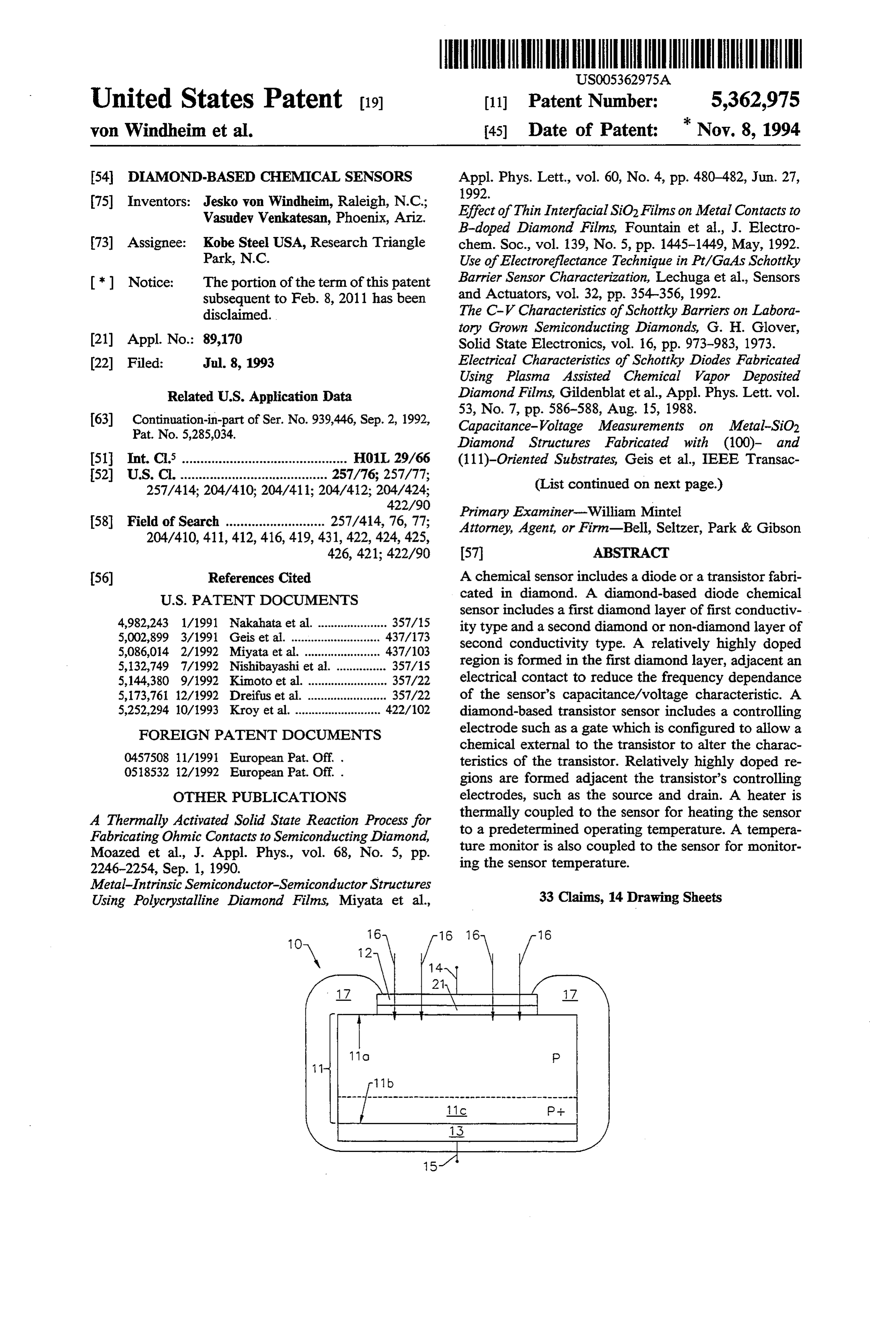
56) References Cited A chemical sensor includes a diode or a transistor fabri
sensor includes a first diamond layer of first conductiv 4,982,243 1/1991 Nakahata et al. ..................... 357/15 ity type and a second diamond or non-diamond layer of 5,002,899 3/1991 Geis et al. ........................... 437/173 second conductivity type. A relatively highly doped 5,086,014 2/1992 Miyata et al. ........ ... 437/103 5,132,749 7/1992 Nishibayashi et al. ............... 357/15 region is formed in the first diamond layer, adjacent an 5,144,380 9/1992 Kimoto et al. ........................ 357/22 electrical contact to reduce the frequency dependance 5,173,761 12/1992 Dreifus et al. ........................ 357/22 of the sensor's capacitance/voltage characteristic. A 5,252,294 10/1993 Kroy et al. .......................... 422/102 diamond-based transistor sensor includes a controlling FOREIGN PATENT DOCUMENTS electrode such as a gate which is configured to allow a chemical external to the transistor to alter the charac 0457508 11/1991 European Pat. Off. . teristics of the transistor. Relatively highly doped re 0518532 12/1992 European Pat. Off. . gions are formed adjacent the transistor's controlling OTHER PUBLICATIONS electrodes, such as the source and drain. A heater is A Thermally Activated Solid State Reaction Process for thermally coupled to the sensor for heating the sensor Fabricating Ohmic Contacts to Semiconducting Diamond, to a predetermined operating temperature. A tempera Moazed et al., J. Appl. Phys., vol. 68, No. 5, pp. ture monitor is also coupled to the sensor for monitor 2246-2254, Sep. 1, 1990. ing the sensor temperature. Metal-Intrinsic Semiconductor-Semiconductor Structures
Using Polycrystalline Diamond Films, Miyata et al., 33 Claims, 14 Drawing Sheets
Page 2
OTHER PUBLICATIONS Thin Film Diamond Microstructures, T. Roppel et al.,
tions on Electron Devices, vol. 38, No. 3, pp. 619-626, Polycrystalline Diamond Device Processing, C. D. Ellis et Mar. 1991. al., IEEE, pp. 222-225, 1991.
Materials Selection for Semiconductor Gas Sensors, P. T. Miniaturized Radiation Detector with Custom Synthesized Moseley, Sensors and Actuators, B.6, pp. 149-156, Diamond Crystal Sensor, J. H. Grobbelaar et al., Nuclear 1992. Instruments and Methods in Physics Research B61, pp. Ceramic Sensor Device Materials, T. Nenov et al., Sen 553-559, 1991.
sors and Actuators, B.8, pp. 117-122, 1992. Piezoresistivity in Vapor-Deposited Diamond Films, M. An Application of Carbon-Type Semiconductors for the Aslam et al., Appl. Phys. Lett., vol. 60, No. 23, pp. Construction of a Humidity-Sensitive Diode, J. P. Lukas 2923-2925, Jun. 8, 1992.
zewicz, Sensors and Actuators, B.6, pp. J. 1992. Diamond Electronics: Sparkling Potential, I. Peterson, Hydrogenated Amorphous Silicon Technology for Chemi Science News, vol. 130, p. 118, 1986. cally Sensitive Thin-Film Transistors, L. Mariucci et al., Improved Tellurium Films by partially Ionized Vapor Sensors and Actuators, B.6, pp. 29-33, 1992. Deposition as the Semiconductor Layer of a TFT and a Annonia Sensitivity of Pt/GaAs Schottky Barrier Diodes. Hydrogen Sensor, K. Okuyama et al., Japanese Journal Improvement of the Sensor with an Organic Layer, L. M. of Applied Physics, vol. 28, No. 5, pp. 770-775, May, Lechuga et al., Sensors and Actuators, B.8, pp. 249-252, 1989.
1992. Diamond-Like Films as a Protecting Insulator for Conductive-Oxide-Gate FET as a Gas Sensor, L. I. Gas-Detecting Suspended-Gate field Effect Transistor, H. Popova et al., Sensors and Actuators, B.3, pp. 273-277, Lorenz et al., Surface and Coatings Technology, 47, pp. 1991. 746-753, 1991.
Physics With Catalytic Metal Gate Chemical Sensors, I. Proceedings of the Conference on Recent Advances in Lundström et al., vol. 15, Issue 3, pp. 201-278, 1989. Adaptive and Sensory Materials and Their Applications, C. Sensor Applications for Synthetic Polycrystalline Thin A. Rogers et al., Center for Intelligent Material Systems Film Diamond, T. Roppel et al., Sensors and Materials, and Structures, Virginia Polytechnic Institute and State 2,6, pp. 329-346, 1991. University, Apr. 27–29, 1992, pp. 254-265.
Page 3
Drawing sheet — no readable text.
Page 4
Drawing sheet — no readable text.
Page 5
Drawing sheet — no readable text.
Page 6
Drawing sheet — no readable text.
Page 7
Drawing sheet — no readable text.
Page 8
Drawing sheet — no readable text.
Page 9
Drawing sheet — no readable text.
Page 10
Drawing sheet — no readable text.
Page 11
Drawing sheet — no readable text.
Page 12
Drawing sheet — no readable text.
Page 13
Drawing sheet — no readable text.
Page 14
Drawing sheet — no readable text.
Page 15
Drawing sheet — no readable text.
Page 16
Drawing sheet — no readable text.
Page 17
Diamond has the highest thermal conductivity of any
DAMOND-BASED CHEMICAL SENSORS solid at room temperature and exhibits good thermal conductivity over a wide temperature range. The high
CROSS REFERENCE TO RELATED thermal conductivity of diamond may be advanta APPLICATION geously used to remove waste heat from an integrated This application is a continuation-in-part of copend circuit, particularly as integration densities increase. Ill ing application Ser.No. 07/939,446 filed Sep. 2, 1992 addition, diamond has a smaller neutron cross-section now U.S. Pat. No. 5,285,034, issued Feb. 8, 1994. which reduces its degradation in radioactive environ ments, i.e., diamond is a “radiation-hard' material.
FIELD OF THE INVENTION 10 Because of the advantages of diamond as a material This invention relates to microelectronic devices, and for semiconductor devices, there is at present an interest more particularly to microelectronic devices fabricated in the growth and use of diamond Schottky diodegas sensors. Unfortunately, it has been found that Schottky of diamond.
diodes fabricated from diamond exhibit frequency de
BACKGROUND OF THE INVENTION 5 pendence of their capacitance/voltage characteristic, Chemical sensors are widely used in industrial envi thereby
Schottky limiting the usefulness of diamond based diodes and gas sensors.
ronments for process control, environmental control, The frequency dependent variation of the capacitan and other applications. As is well known to those hav ce/voltage characteristic of diamond based Schottky ing skill in the art, a chemical sensor is a device which 20 devices has been widely investigated. See, for example, monitors the concentration of a given chemical species in a liquid or a gas. Chemical sensors are often required the publications entitled The C-V Characteristics of Schottky barriers on Laboratory Grown Semiconducting to be highly sensitive, in order to detect small concen Diamonds by Glover, Solid State Electronics, Vol. 16, trations of the chemical. They are also often required to pp. 973-983 (1973); and Electrical Characteristics of withstand harsh chemical environments and/or high 25 Schottky Diodes Fabricated Using Plasma Assisted Chem temperatures which may be present in process control, ical Vapor Deposited Diamond Films by Gildenblat et al., environmental control or other applications. Applied Physics Letters, Vol. 53, No. 7, pp. 586-588 One form of chemical sensor is a gas sensor. Schottky (1986).
diodes are widely used as gas sensors. As is well known In these investigations, the frequency dependent vari to those having skill in the art, a diode exhibits a very 30 ation in capacitance/voltage characteristic has been low resistance to current flow in one direction and a attributed to the presence of deep level states in the very high resistance to current flow in the opposite diamond band gap, and to the high resistivity of bulk direction, thereby producing current rectification. As is diamond as a result of diamond's unique energy level also well known to those having skill in the art, a structure. Accordingly, characterizations of Schottky Schottky diode produces rectification as a result of 35 contacts have heretofore assumed that the undesirable nonlinear current transport across a metal-semiconduc frequency dependence of the capacitance/voltage char tOT COntact. acteristic was as a result of the inherent energy level For example, a Schottky diode using a catalytic metal structure (i.e. the deep level states in the diamond band contact such as platinum or palladium, has been shown gap) and high series resistance of the diamond material to be an excellent hydrogen gas sensor. In a Schottky itself. This undesirable frequency dependence limits the diode, the Schottky barrier height decreases when the usefulness of diamond based gas sensors, notwithstand device is exposed to a hydrogen containing atmosphere. ing the advantages of diamond as a material for semi The hydrogen induced changes are typically detected conductor devices, especially in high frequency or fast as a modification of the capacitance voltage (C-V) or transient applications.
the current voltage (I-V) characteristics of the diode. 45
See, for example, a publication entitled Use of the Elec SUMMARY OF THE INVENTION troreflectance Technique in Pt/GaAs Schottky Barrier It is therefore an object of the invention to provide Sensor Characterization by Lechuga et al., Sensors and diamond-based chemical sensors.
Actuators, Vol. 32, pp. 354-356, 1992. It is another object of the invention to provide dia Diamond is a preferred material for semiconductor 50 mond-based chemical sensors which exhibit reduced devices because it has semiconductor properties that are frequency dependence of their capacitance/voltage better than silicon, germanium or gallium arsenide. characteristic.
Diamond provides a higher energy bandgap, a higher These and other objects are provided, according to breakdown voltage and a higher saturation velocity the present invention, by a chemical sensor which in than these traditional semiconductor materials. 55 cludes a diode or a transistor fabricated in diamond. A These properties of diamond yield a substantial in diamond based diode chemical sensor includes a first crease in projected cutoff frequency and maximum diamond layer of first conductivity type and a second operating voltage compared to devices fabricated using semiconductor layer of second conductivity type on the silicon, germanium or gallium arsenide. Silicon is typi first diamond layer. The first and second layers form a cally not used attemperatures higher than about 200 C. semiconductor junction therebetween. The second and gallium arsenide is not typically used above 300 C. layer may be a second diamond layer. At least one of These temperature limitations are caused, in part, be the first and second layers is configured to allow a cause of the relatively small energy band gaps for sili chemical which is external to the sensor to interact with con (1.12 eV at ambient temperature) and gallium arse the first or second layer and alter an electrical charac nide (1.42 Ev at ambient temperature). Diamond, in 65 teristic of the semiconductor junction. For example, at contrast, has a large band gap of 5.47 Ev at ambient least one of the first and second layers is configured to temperature, and is thermally stable up to about 1400 allow absorption/adsorption of gas molecules or atoms, C. resulting in a change in the surface potential, conductiv
Page 18
ity, charge density or other characteristic. These thereon, wherein the diamond layer includes a highly changes may be detected by detecting shifts in the ca doped region adjacent the ohmic contact to provide a pacitance voltage (C-V) characteristics of the diode. low resistance ohmic contact. It has been found, ac In a particular embodiment of a diamond based diode cording to the invention, that the frequency depen chemical sensor, the first diamond layer is a P-type dence of the capacitance/voltage characteristic of gas diamond layer and the second layer includes an N-type sensors formed thereby is not primarily related to the gas sensitive second diamond layer. The second layer presence of deep level states in the diamond band gap, can also be an N-type moisture sensitive second layer, as has been assumed for a period of over twenty years. an N-type gas sensitive semiconducting oxide layer, an Rather, according to the invention, it has been found N-type carbon layer or another N-type chemical sensi 10 that the strong frequency dependence is primarily a tive layer. Preferably, the first diamond layer is rela result of the high impedance (i.e. resistance and capaci tively lightly doped and an electrical contact is formed tance) of the "ohmic' contact which is typically applied on the first diamond layer. A relatively highly doped region is formed in the first diamond layer, adjacent the to the diamond layer. The high series resistance of diamond also plays an important role in the frequency electrical contact, so that the electrical contact forms an 15 dependence, as has already been known. When the ohmic contact with the highly doped region. When the diamond layer includes a highly doped region adjacent diamond layer includes a highly doped region adjacent the ohmic contact, the frequency dependence of the the ohmic contact, the frequency dependence of the capacitance/voltage characteristic is reduced signifi capacitance/voltage characteristic is reduced signifi cantly. Gas sensors with improved operational charac cantly. 20 teristics are thereby provided.
A diamond based transistor chemical sensor includes
According to the invention, the highly doped region a diamond layer and a field effect or bipolar transistor in adjacent the diamond layer. The transistor includes a controlling the ohmic contact is preferably boron doped at electrode, such as a gate or base electrode and first and a concentration of at least 1020 cm3. This doping forms second controlled electrodes such as source and drain 25 an ohmic contact with a contact resistance of less than electrodes or emitter and collector electrodes. The con 103 0-cm2. Preferably, the ohmic contact is a back trolling electrodes are configured to allow a chemical contact on a face of a diamond layer opposite the external to the diamond based transistor to interact with Schottky contact.
the controlling electrode or the diamond layer, and The diamond layer of the present invention can be a alter the characteristics of the transistor. For example, 30 monocrystalline diamond layer or a polycrystalline the controlling electrode may include a gas sensitive or diamond layer. The diamond layer may itself be formed moisture sensitive layer. As also described above, a on a diamond or a nondiamond substrate using tech highly doped diamond layer is preferably formed adja niques well known to those having skill in the art. When cent the controlled electrodes (such as the source and a back ohmic contact is formed on the diamond layer, a drain) to form ohmic contacts and thereby reduce the 35 portion of the substrate is preferably removed to expose frequency dependence of the capacitance/voltage char the back face of the diamond layer, opposite the acteristic of the transistor. Schottky contact, and allow the highly doped boron According to another aspect of the invention, the region to be formed. A metal contact is formed on the diamond based diode or transistor chemical sensor in boron doped region.
cludes a heater which is thermally coupled to the sensor The highly doped boron region can be formed in the for heating the sensor to a predetermined temperature. diamond layer by in situ boron doping or boron ion Since diamond is capable of operating effectively at implantation using techniques well known to those hav high temperatures, the heater may be provided to in ing skill in the art. By providing a highly doped boron crease the chemical sensitivity of the sensor by elevat layer adjacent the ohmic contact, frequency variations ing the temperature of the sensor. The heater can also 45 of the capacitance/voltage characteristics are reduced. be used to purge the chemical sensor or to move the A gas sensor according to the invention includes a sensor between operating temperatures to enhance sen diamond layer having first and second opposing faces, sitivity to different chemical species. A temperature and a first contact on the first face, wherein the first monitor is also preferably coupled to the sensor for monitoring the temperature of the sensor. An accurate 50 contact
Schottky forms a Schottky barrier of predetermined barrier height between the first contact and indication of the sensing temperature is thereby ob the first face. The first contact allows gas to interact tained. Preferably, the heater is an interdigitated resis with the first face, to thereby alter the predetermined tive heater which is formed in one of the diamond layers Schottky barrier height. The contact is preferably a of the diode or transistor, and the temperature monitor catalytic metal contact such as platinum or palladium, is preferably a diamond-based thermistor. 55 which is sufficiently thin to allow gas to interact with
Diamond-based diode or transistor chemical sensors according to the present invention may operate in high istheless diamond layer. Preferably the catalytic metal layer than 1000 $) thick. When the diamond layer is a temperature environments, in which conventional chemical sensors may not operate. They may also oper layer of polycrystalline diamond, a layer of undoped ate in corrosive environments in which conventional diamond or a thin layer of silicon dioxide is also prefera sensors may not operate without extensive encapsula bly included between the metal layer and the polycrys tion and other protection. Moreover, because they are talline diamond layer. The gas sensor also includes a based on diamond semiconductor, they can be inte second contact, preferably on the second face, and the grated with transistors and other devices to form con diamond layer includes a highly doped region, prefera trol or other circuits used with the chemical sensor. 65 bly boron doped at a concentration of at least 1020 According to another aspect of the invention, a dia cm3, adjacent the second contact, to form an ohmic mond-based gas sensor includes a diamond layer having contact having a contact resistance of less than 103 a Schottky contact thereon and an ohmic contact ()-cm2. An improved gas sensor is thereby provided.
Page 19
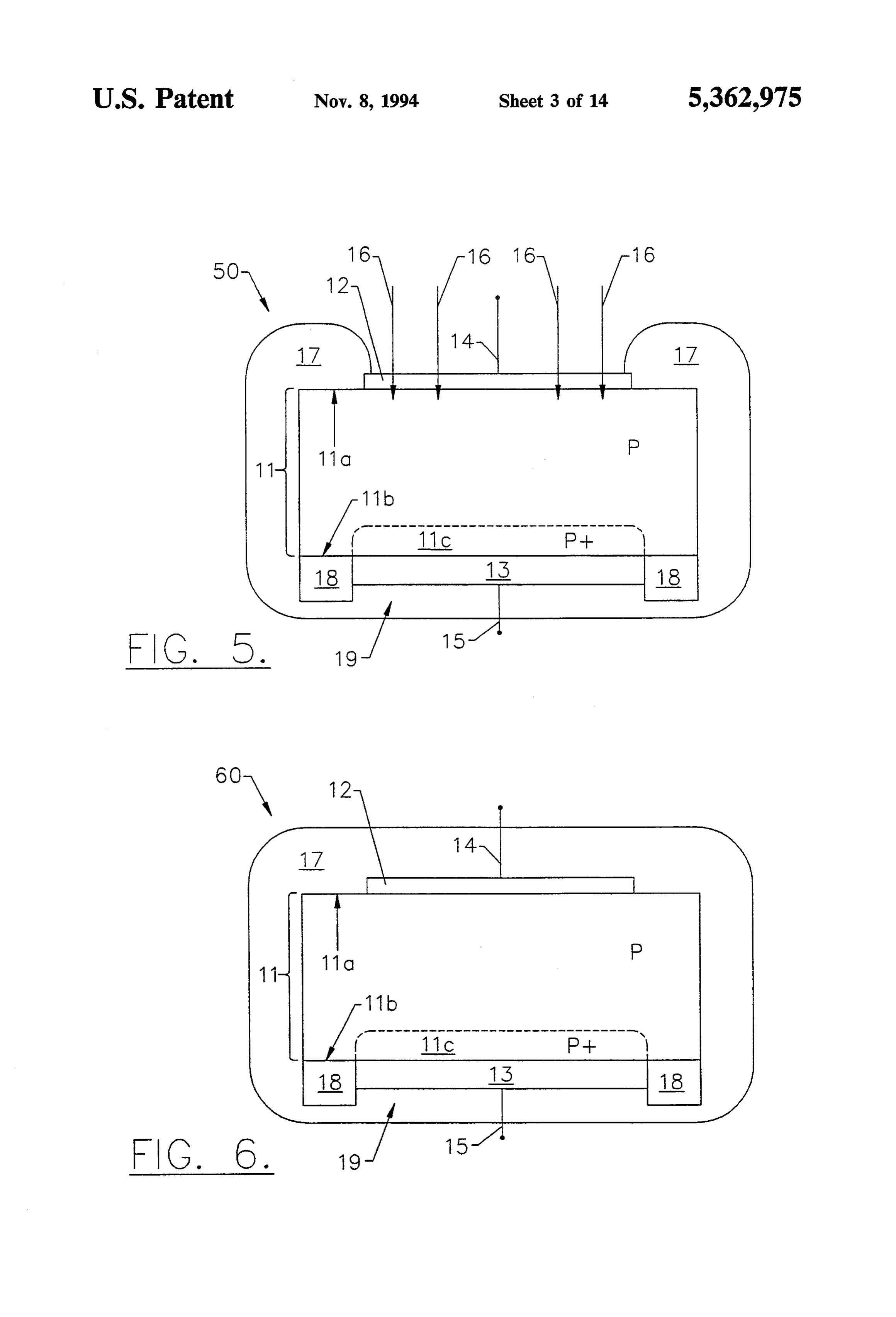
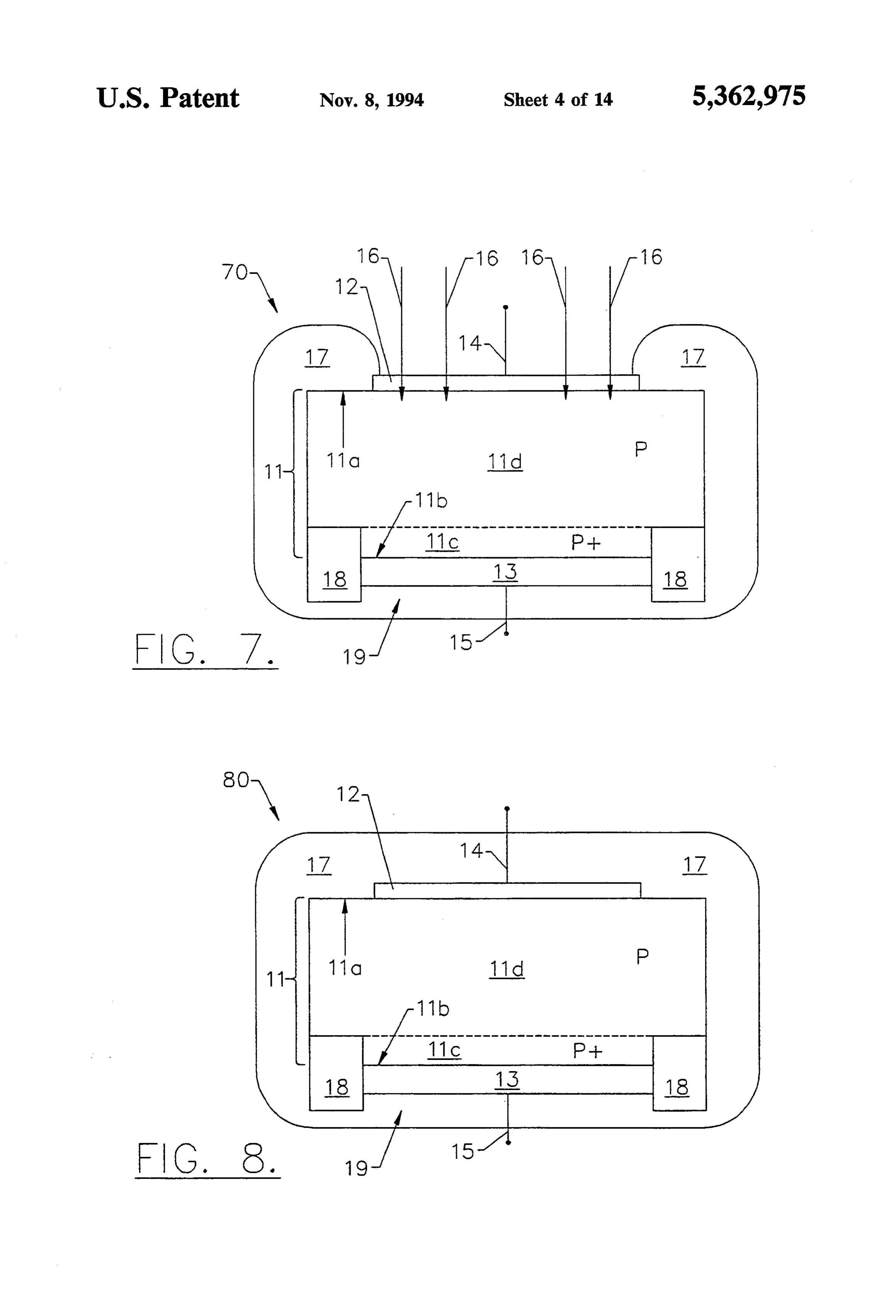
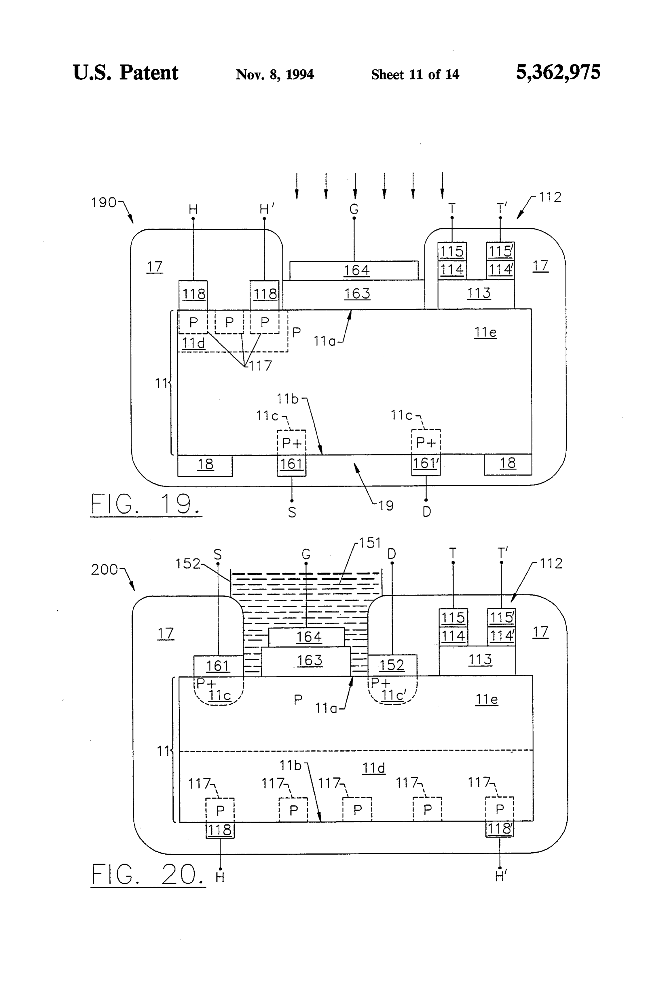
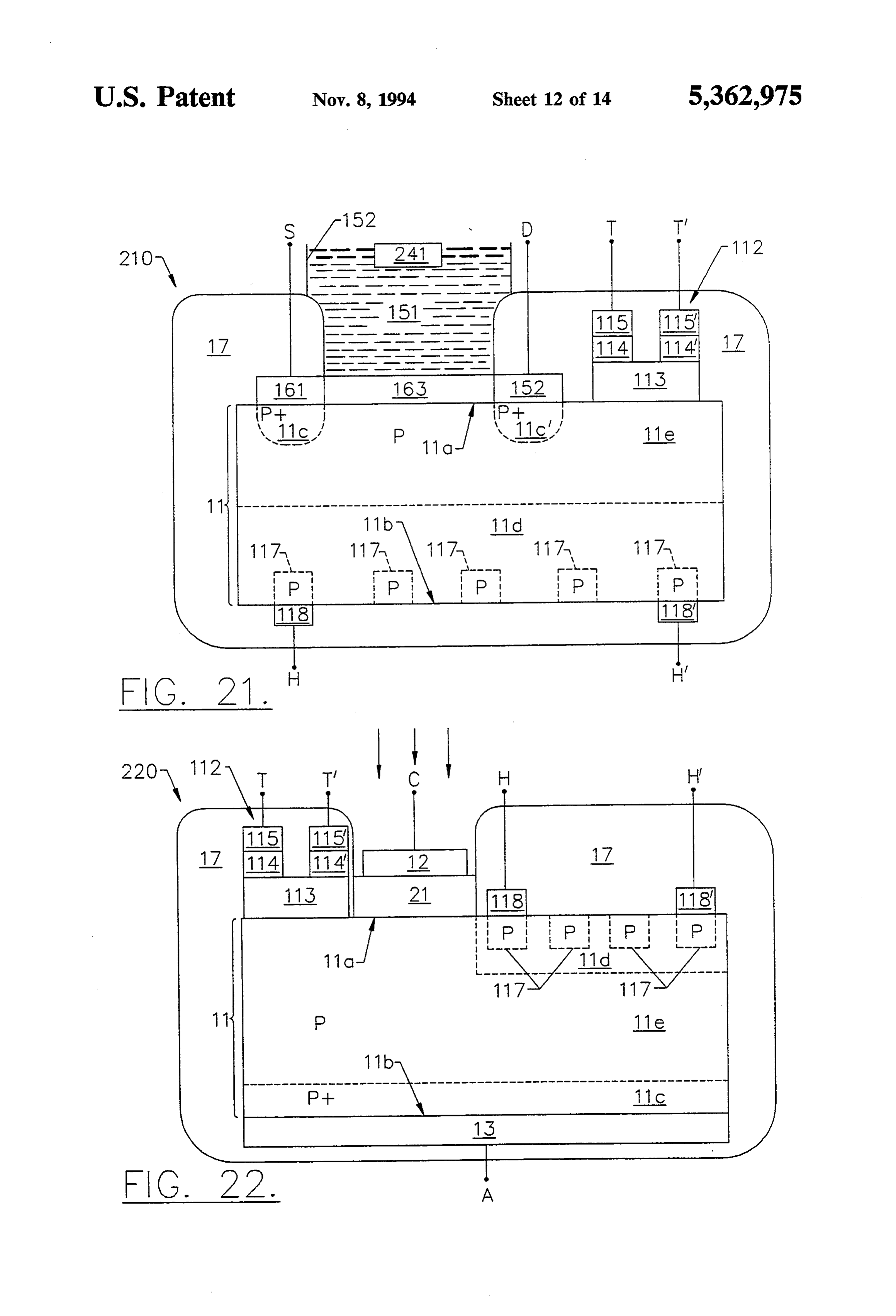
FIG. 21 illustrates a cross-sectional view of a sixth
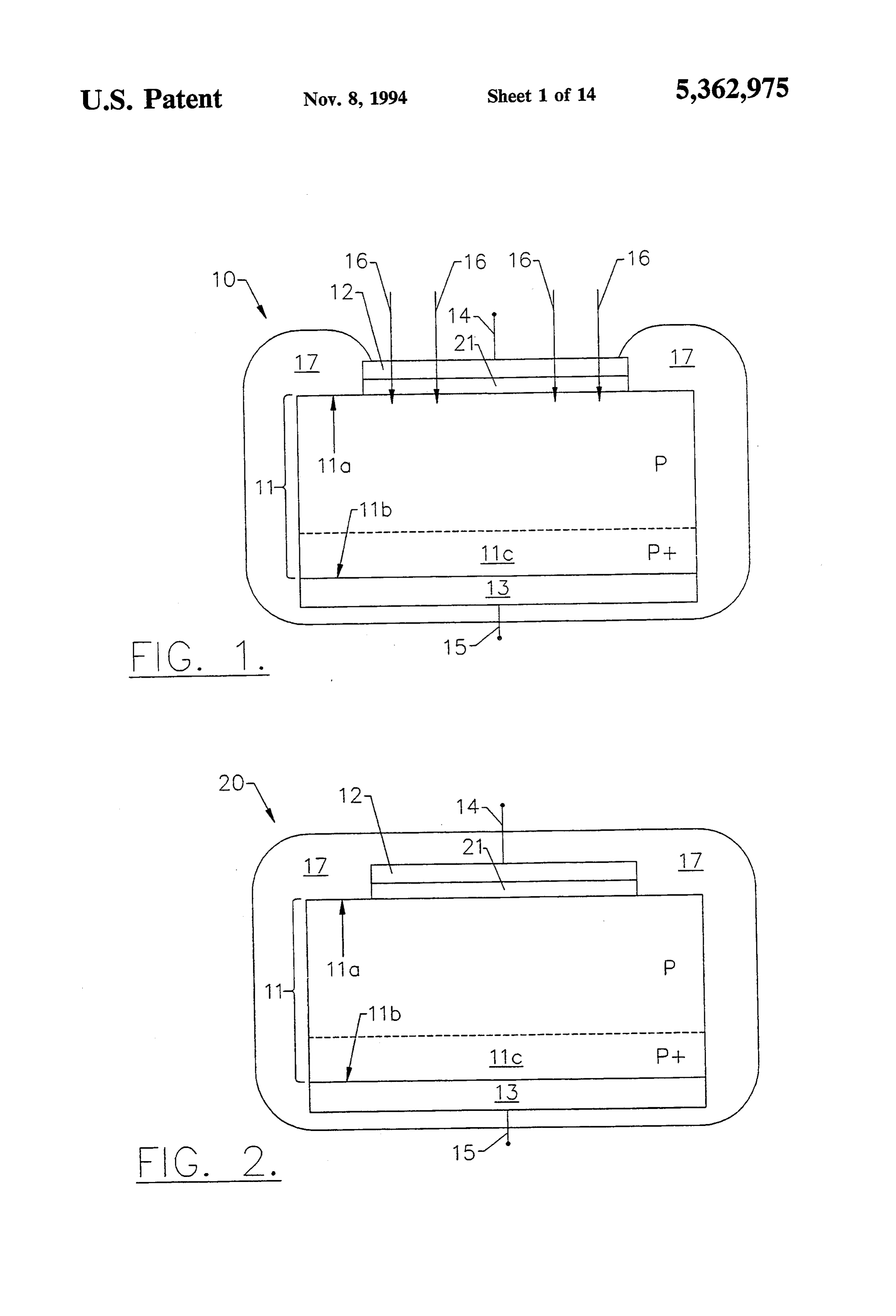
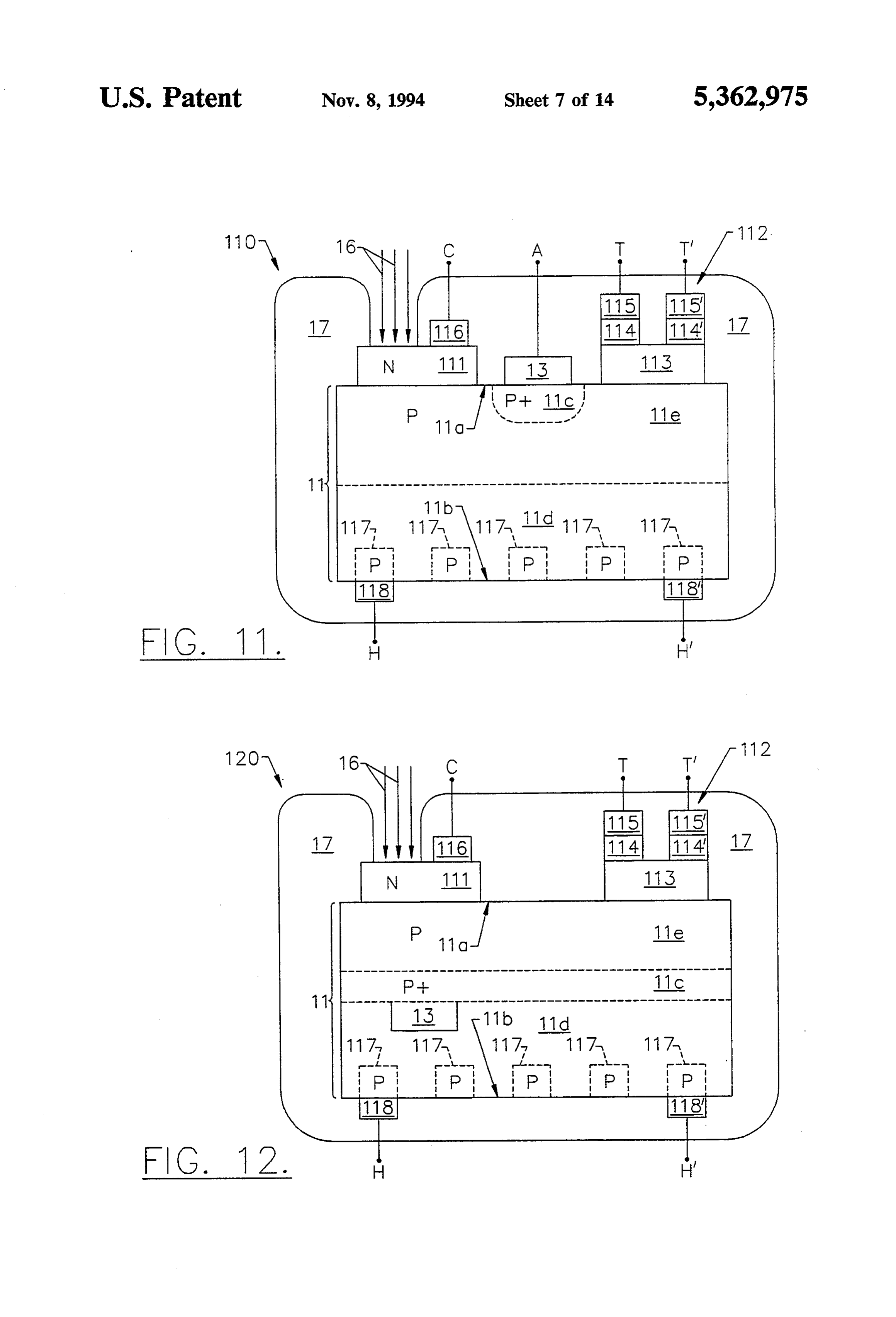
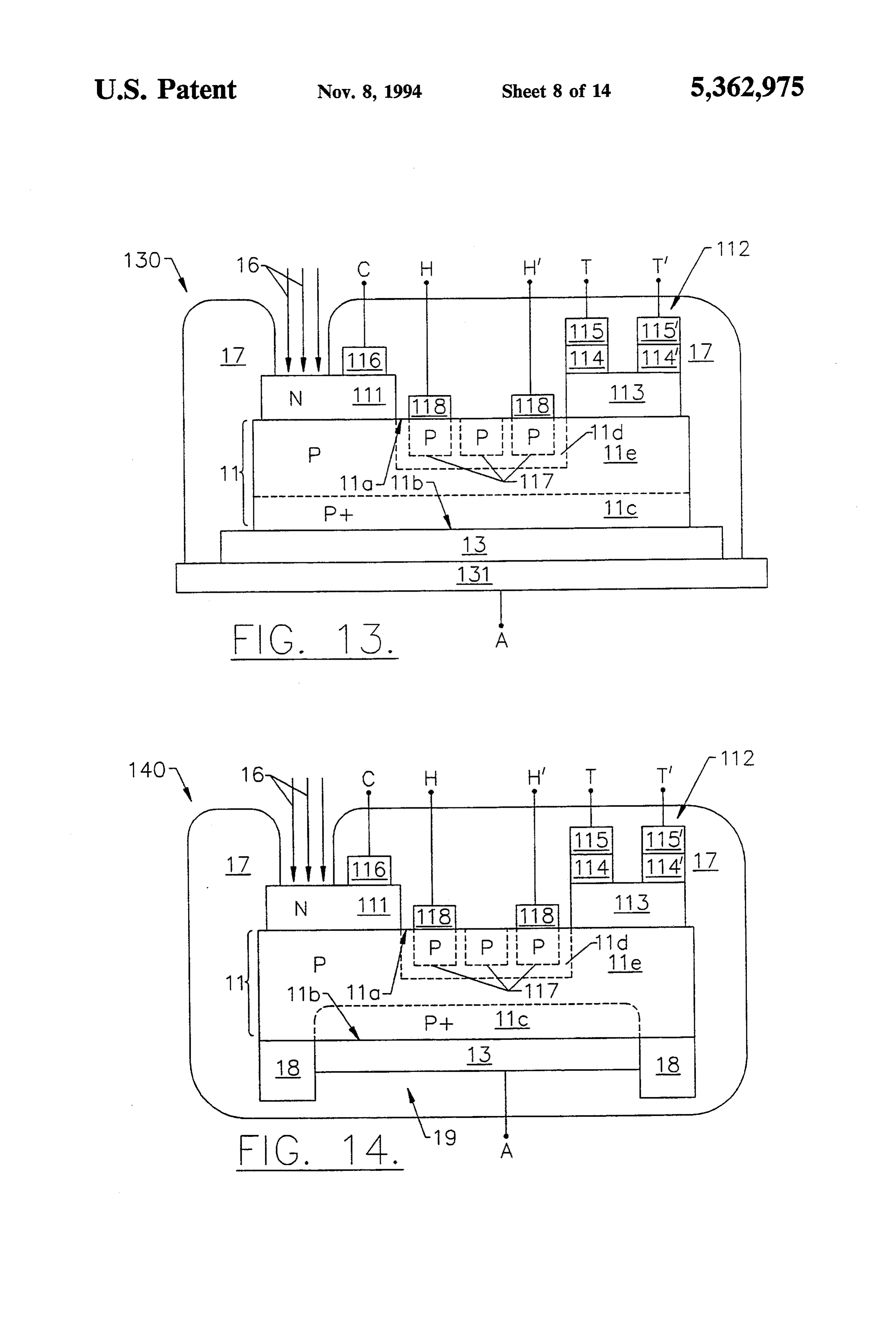
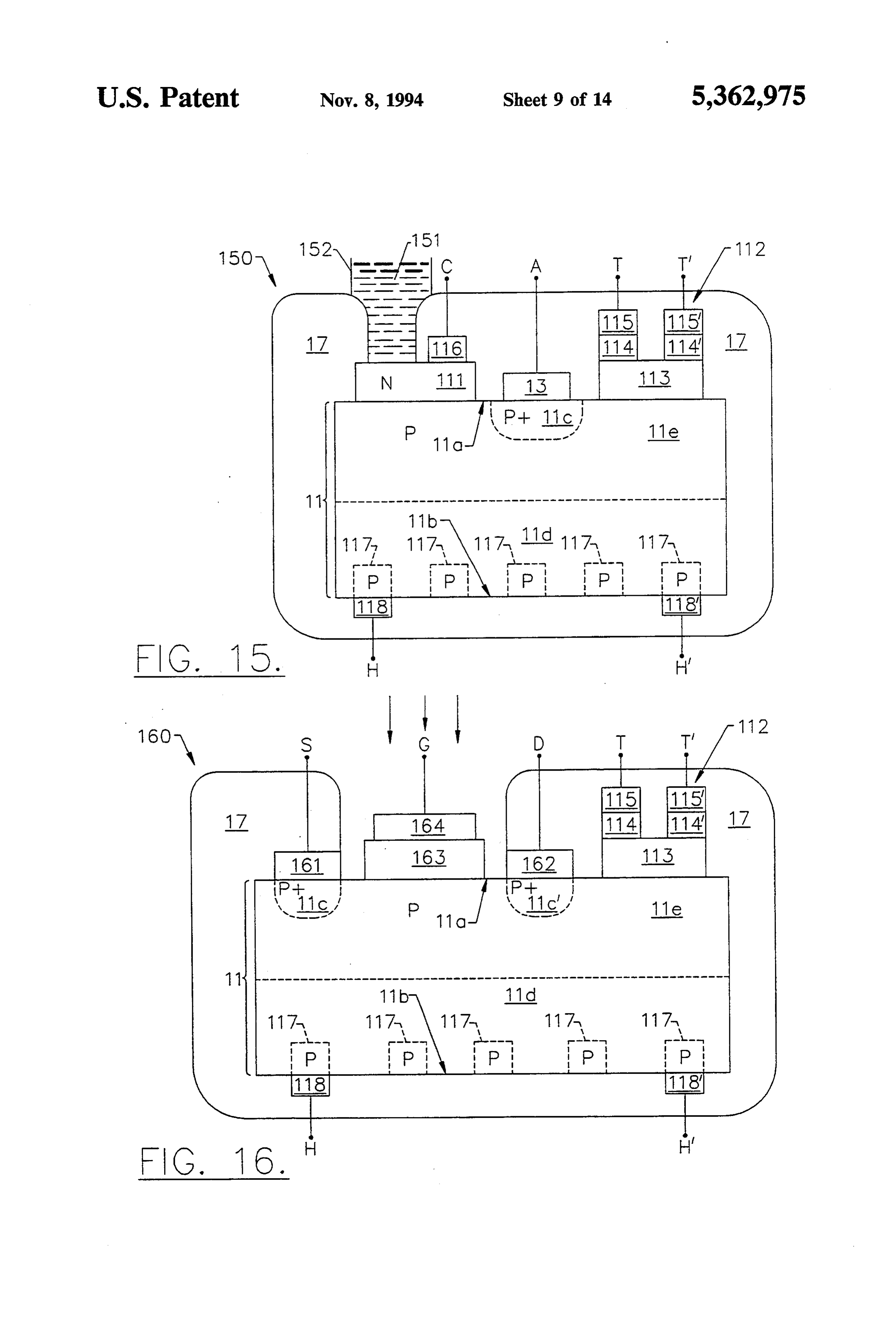
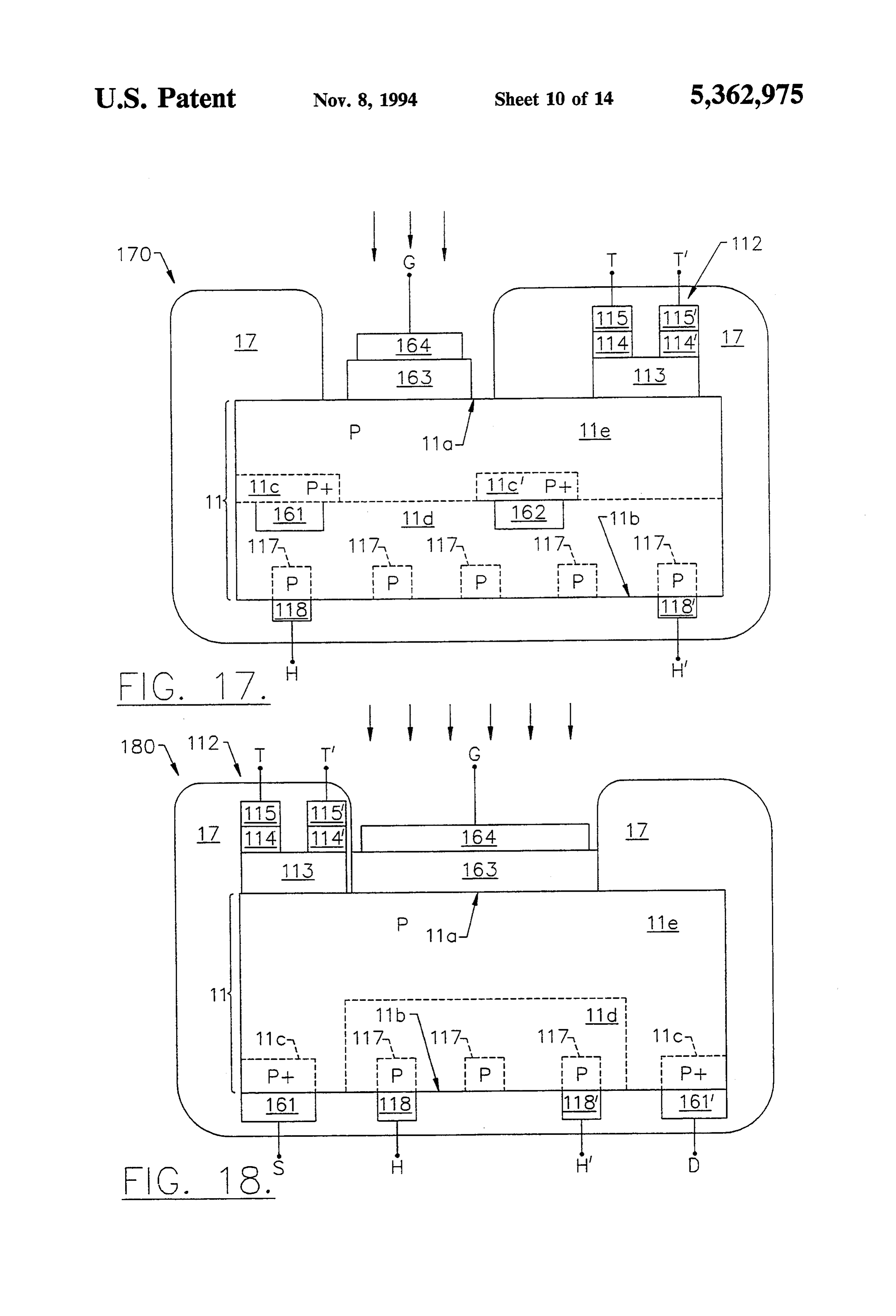
BRIEF DESCRIPTION OF THE DRAWINGS embodiment of a diamond-based transistor chemical FIG. 1 illustrates a cross-sectional view of a first sensor according to the present invention. embodiment of a gas sensor according to the present FIG. 22 illustrates a cross-sectional view of an ele invention. 5 vated temperature chemical sensor according to the FIG.2 illustrates a cross-sectional view of a first em present invention.
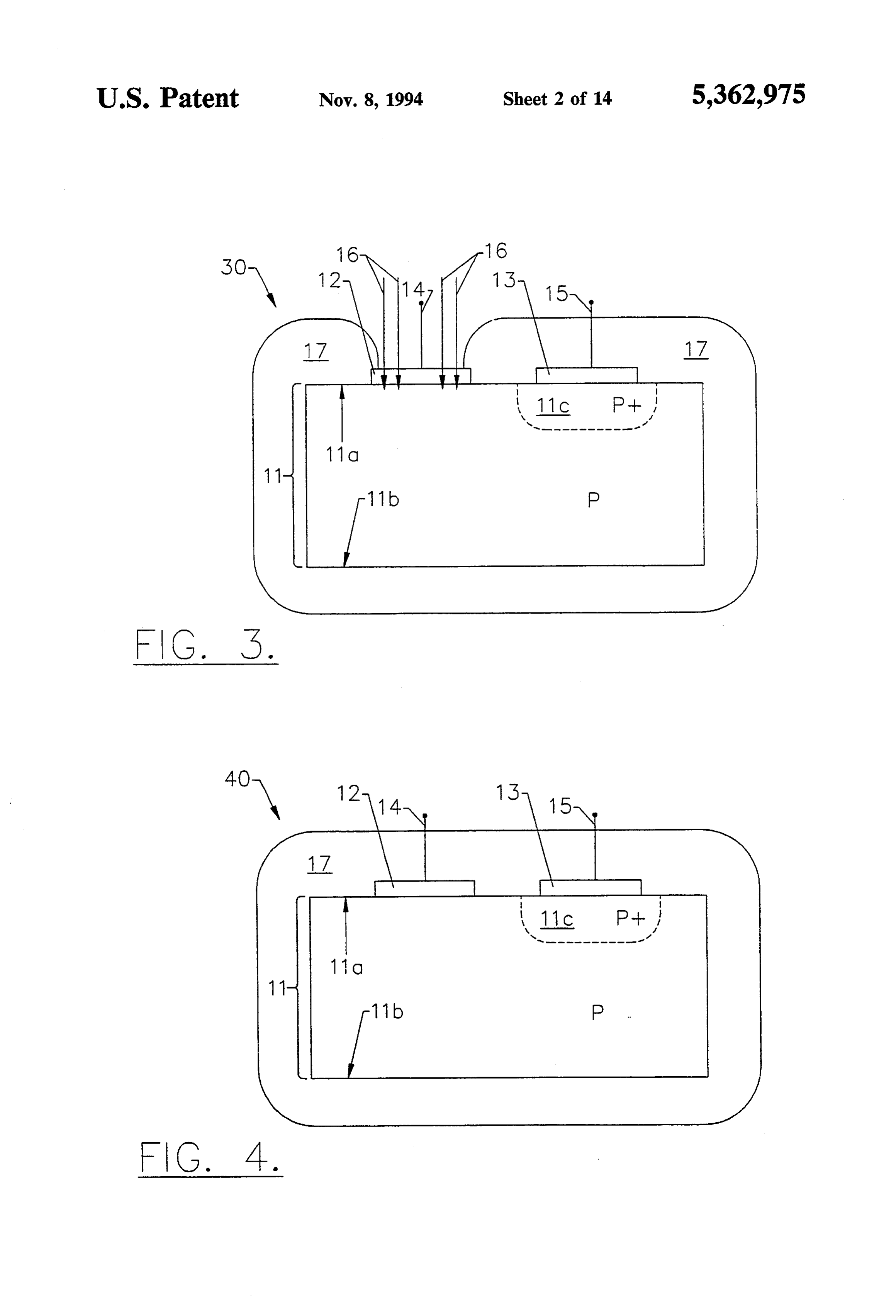
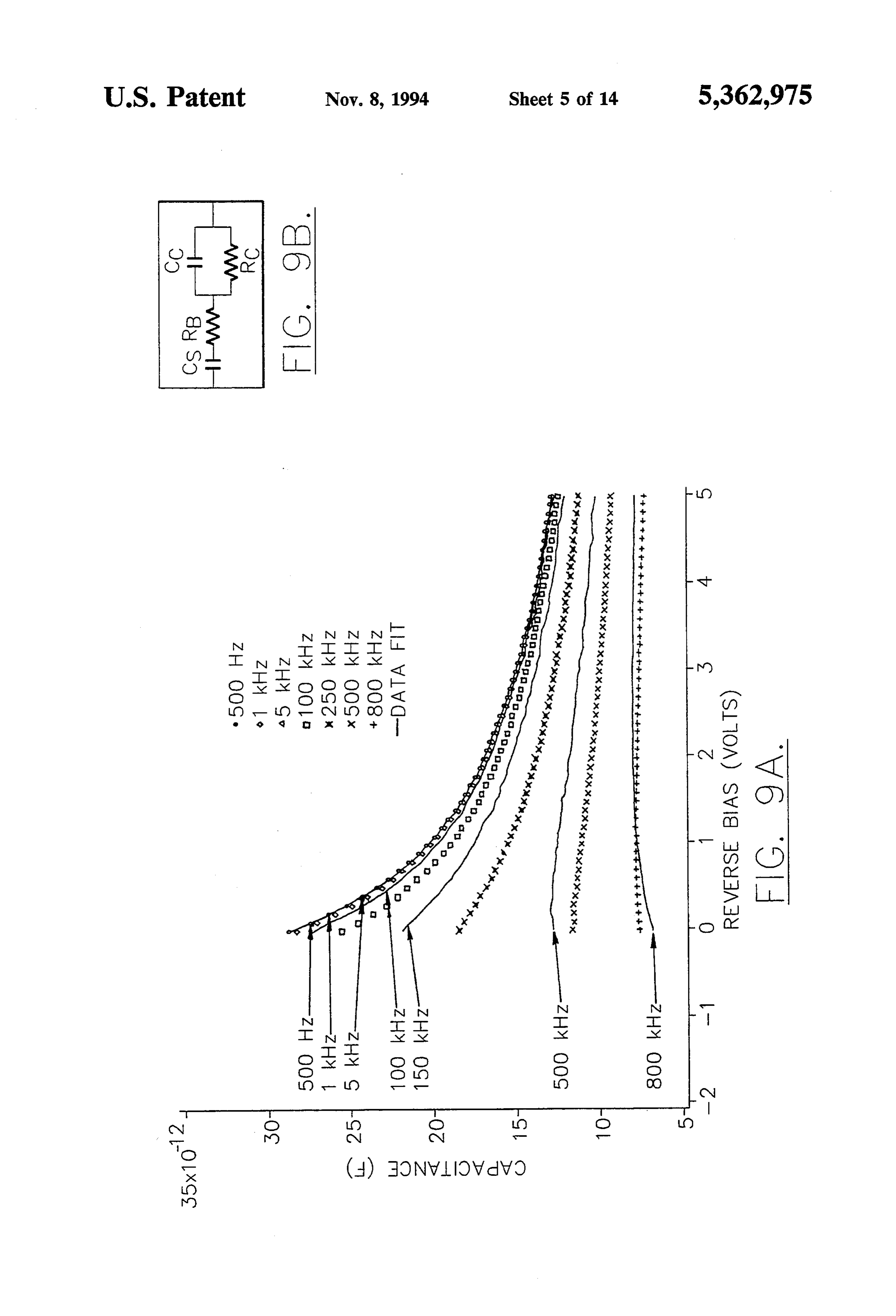
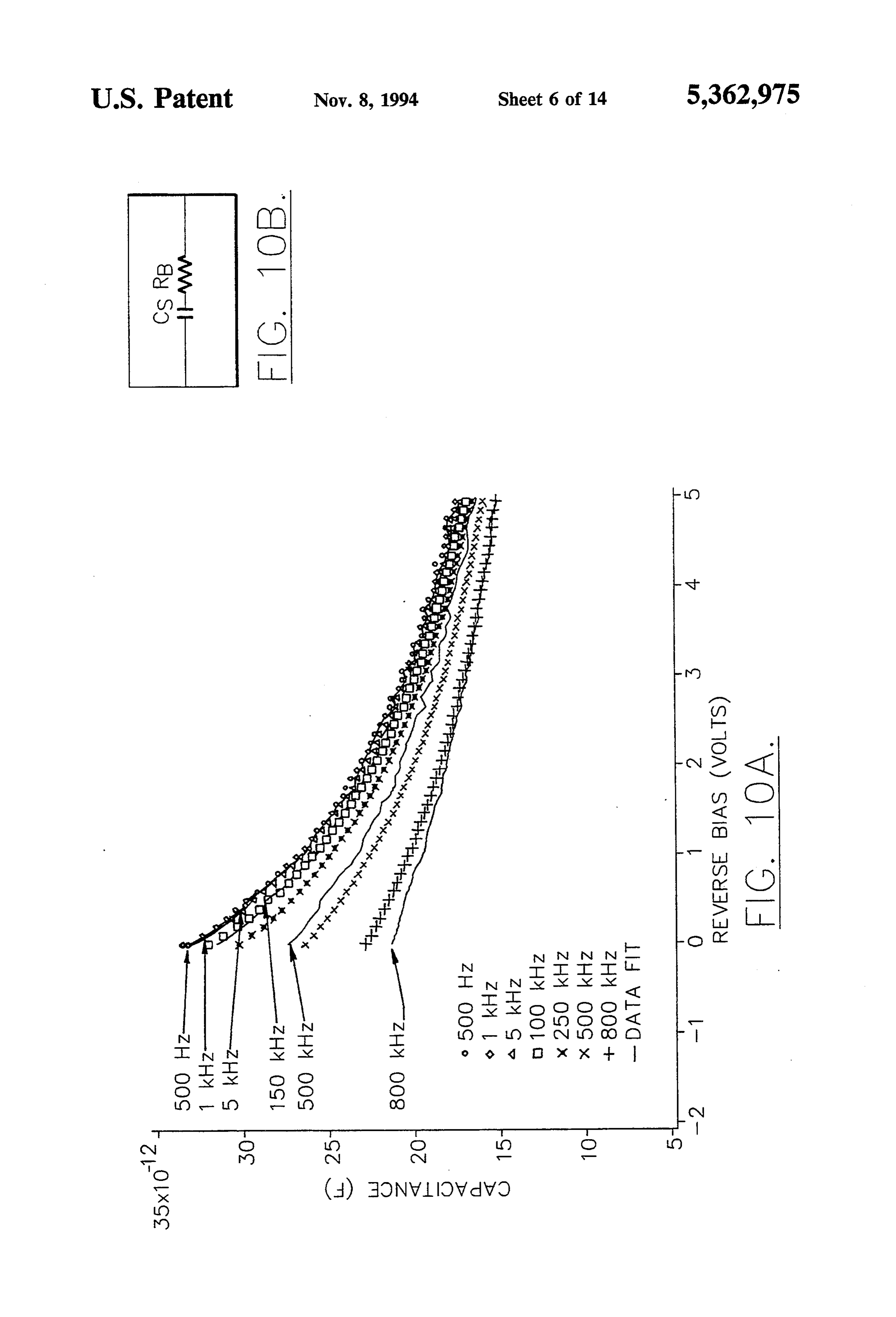
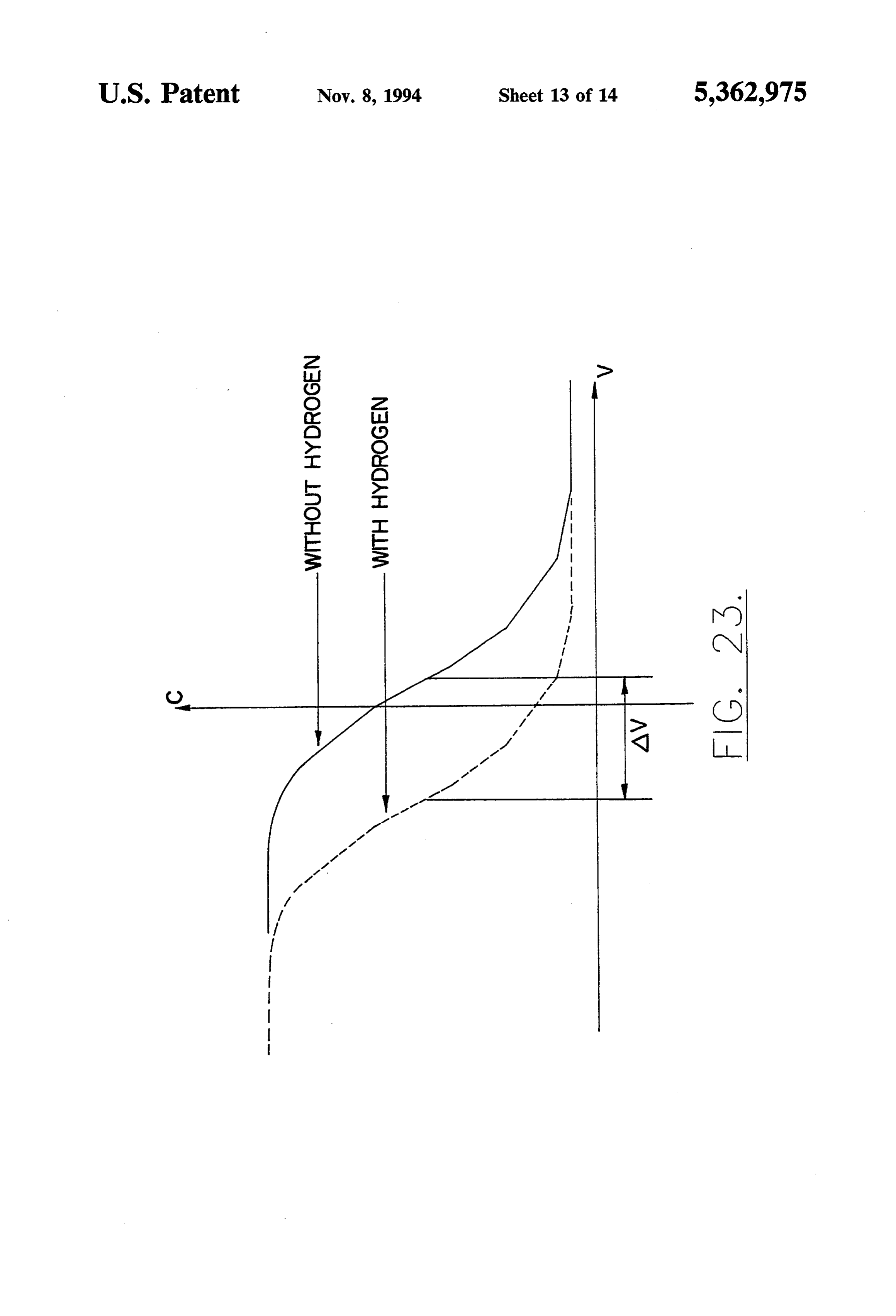
bodiment of a Schottky diode according to the present tance FIG. 23 graphically illustrates representative capaci invention. versus voltage changes for the diode chemical FIG. 3 illustrates a cross-sectional view of a second sensors of FIGS. 11-15.
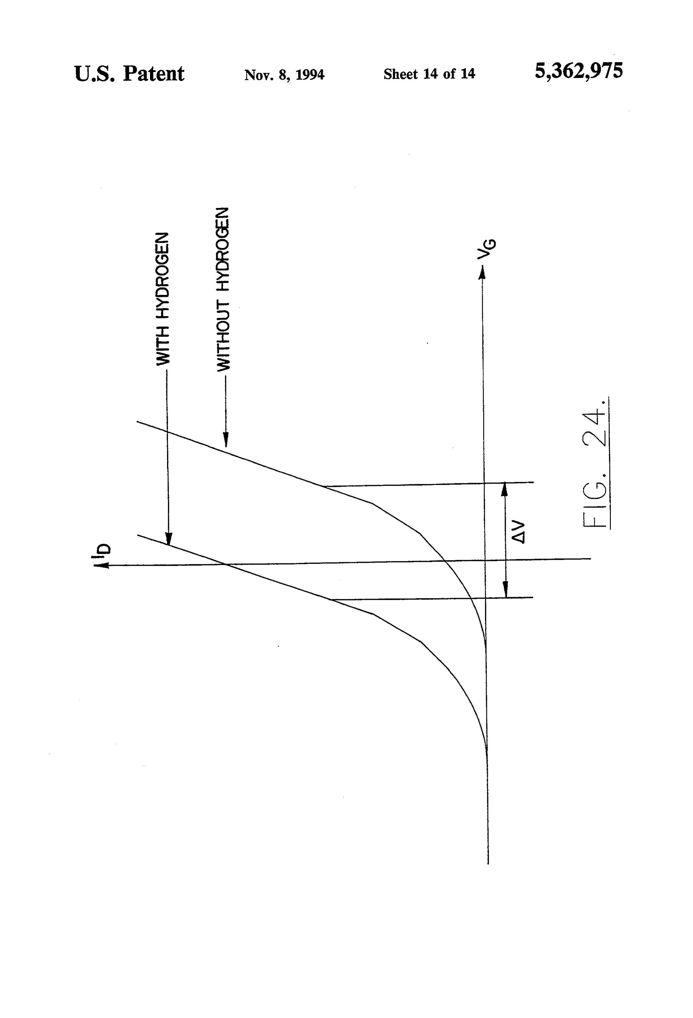
embodiment of a gas sensor according to the present 10 FIG. 24 graphically illustrates changes in transistor characteristics for the transistor based sensors of FIGS.
invention. 16-21.
FIG. 4 illustrates a cross-sectional view of a second embodiment of a Schottky diode according to the pres DESCRIPTION OF THE PREFERRED ent invention. 15 EMBODIMENTS FIG. 5 illustrates a cross-sectional view of a third The present invention now will be described more embodiment of a gas sensor according to the present fully hereinafter with reference to the accompanying invention. drawings, in which preferred embodiments of the in FIG. 6 illustrates a cross-sectional view of a third vention are shown. This invention may, however, be embodiment of a Schottky diode according to the pres 20 embodied in many different forms and should not be ent invention. construed as limited to the embodiments set forth FIG. 7 illustrates a cross-sectional view of a fourth herein; rather, these embodiments are provided so that embodiment of a gas sensor according to the present this disclosure will be thorough and complete, and will invention. fully convey the scope of the invention to those skilled FIG. 8 illustrates a cross-sectional view of a fourth 25 in the art. In the drawings, the thickness of layers and embodiment of a Schottky diode according to the pres regions and positions of grain boundaries are exagger ent invention. ated for clarity. Like numbers refer to like elements FIGS. 9A and 9B are a graphical illustration of throughout.
Capacitance-Voltage measurements as a function of Referring now to FIG. 1, a first embodiment of a frequency for a conventional Schottky diode, and an 30 diamond gas sensor according to the present invention equivalent circuit for the conventional Schottky diode, is shown. Gas sensor 10 includes a diamond layer 11, respectively. preferably between about 1 p.m. and about 250 um thick, FIGS. 10A and 10B are a graphical illustration of and which is lightly doped, preferably at a boron con Capacitance-Voltage measurements as a function of centration of 1015-1018 atoms cm3. Diamond layer 11 frequency for a Schottky diode according to the present 35 may be a monocrystalline diamond layer or a polycrys invention, and an equivalent circuit for a Schottky talline diamond layer and may be formed using tech diode according to the present invention, respectively. niques well known to those having skill in the art. FIG. 11 illustrates a cross-sectional view of a first Diamond layer 11 includes a first face 11a and a second embodiment of a diamond-based diode chemical sensor face 11b. Other high bulk resistance semiconductors, according to the invention. such as silicon carbide or gallium nitride may be used. FIG. 12 illustrates a cross-sectional view second em As also shown in FIG. 1, diamond layer 11 includes a bodiment of a diamond-based diode chemical sensor highly doped region 11c at second face 11b. Layer 11c according to the invention. is preferably between about 0.3 um and about 1 um FIG. 13 illustrates a cross-sectional view of a third thick and is heavily doped with boron at 1020-1021 embodiment of a diamond-based diode chemical sensor 45 atoms cm-3 to produce a P---- region. according to the invention. Still referring to FIG. 1, a Schottky contact 12 is FIG. 14 illustrates a cross-sectional view of a fourth formed on first face 11a of diamond layer 11. Schottky embodiment of a diamond-based diode chemical sensor contact 12 is formed of a metal which forms a Schottky according to the invention. barrier with diamond. Schottky contact 12 is preferably 50 formed of a catalytic metal such as platinum or palla
FIG. 15 illustrates a cross-sectional view of a fifth dium. The catalytic metal allows the sensing gas to embodiment of a diamond-based diode chemical sensor rapidly pass therethrough in a direction shown by ar according to the invention. rows 16 and interact with the first face 11a of diamond FIG. 16 illustrates a cross-sectional view of a first layer 11. Schottky contact 12 is preferably sufficiently embodiment of a diamond-based transistor chemical 55 thin to allow the gas to interact with the diamond layer. sensor according to the present invention. When platinum prpalladium is used, a thickness of less FIG. 17 illustrates a cross-sectional view of a second than about 100 A is preferred.
embodiment of a diamond-based transistor chemical As described above, diamond layer 11 may be a sensor according to the present invention. monocrystalline diamond layer or a polycrystalline FIG. 18 illustrates a cross-sectional view of a third diamond layer. When a monocrystalline diamond layer embodiment of a diamond-based transistor chemical is used, the Schottky contact 12 is typically formed sensor according to the present invention. directly on the first face 11a of monocrystalline FIG. 19 illustrates a cross-sectional view of a fourth diamond layer 11. However, when a polycrystalline embodiment of a diamond-based transistor chemical diamond layer is used, a Schottky contact is preferably sensor according to the present invention. 65 formed by including an intermediate layer 21 between FIG. 20 illustrates a cross-sectional view of a fifth the metal 12 and the polycrystalline diamond layer 11. embodiment of a diamond-based transistor chemical This intermediate layer is preferably a layer of undoped sensor according to the present invention. (insulating) diamond, about 2000 A thick, as described
Page 20
in the publication by Miyata et al. entitled Metal-Intrin the first face 11a (FIG. 3 or FIG. 4) of diamond layer sic Semiconductor-Semiconductor Structures Using Poly 11, as appropriate, with boron. The implantation dose is crystalline Diamond Films, Applied Physics Letters, preferably 5x 1016 cm-2 at an energy of 60 keV and a Vol. 60, No. 4 (1992), pp. 480-482. Alternatively, inter target temperature of 200 C. The diamond crystals are mediate layer 21 may be a very thin layer of silicon then annealed in a furnace at about 1200° C. for 30 dioxide (SiO2), about 20 A thick, between metal layer minutes at 1x10⁻⁷ Torr. The graphite formed during 12 and polycrystalline diamond layer 11, as described in implantation and annealing is then etched in CrO3--Ha publication by coinventor V. Venkatesan et al. enti 2SO4 acid solution at about 200 C. A high atomic boron tled Effect of Thin Interfacial SiO2 Films on Metal concentration at the appropriate surface 11a (FIG. 1 or Contacts to B-Doped Diamond Films, Journal of the 10 FIG. 2) or 11b (FIG. 3 or FIG. 4) of 1020-1021 cm-3 is Electrochemical Society, Vol. 139, No. 5 (1992), pp. obtained.
1445-1449. Then, metal contact 13 is formed using a refractory As is well known to those having skill in the art, the metal, preferably titanium, about 200 A to about 400 A gas which enters substrate 11, as shown by arrows 16, thick. Other refractory metals may also be used. A gold alters the barrier height of the Schottky barrier formed 15 passivating layer, preferably about 1000A to about 1500 between contact 12 and face 11a. This change in barrier A thick may then be formed on the refractory metal height is used as a criteria for detecting the gas, using layer. Other passivating layers may also be used. An techniques well known to those having skill in the art. anneal may then be performed at about 800 C. to about Heretofore, the frequency dependence of the capaci 850° C. for a time period of about fifteen minutes to tance of the Schottky contact was a strong influence in 20 about ninety minutes, to convert at least a portion of the the determination of barrier height. It was thought that titanium layer to titanium carbide. A low resistance this frequency dependence was due to the presence of source contact is thereby formed. The process for form deep level states in the diamond band gap and to the ing the ohmic contact layer 13 is similar to the process high resistivity of the diamond layer 11. Accordingly, for forming ohmic contacts on diamond as described by the inherent characteristics of diamond itself were here 25 Moazed et al. in A Thermally Activated Solid State Reac tofore thought to be limiting factor in the performance tion Process for Fabricating Ohmic Contacts to Semicon of gas sensors. ducting Diamond, Applied Physics Journal, Vol. 68, No. According to the invention, an ohmic contact is 5, September 1990.
formed of metal 13 on the second face 11b of diamond Referring now to FIG. 5, a third embodiment of the layer 11, adjacent the highly doped region 11c. The 30 gas sensor according to the invention is described. Gas highly doped region preferably produces a contact sensor 50 is similar to gas sensor 10 described in FIG. 1 resistance of less than 10-30-cm2. A first and second except that diamond layer 11 is itself formed on a sub electrode 14 and 15 respectively, connect the Schottky strate 18. The substrate 18 may be a diamond substrate contact 12 and ohmic contact 13 respectively, Suitable or a nondiamond substrate. To facilitate formation of a encapsulation 17 is used to protect the device, while 35 monocrystalline diamond layer 11, substrate 18 is pref allowing gas to interact with the diamond layer 11 at erably crystalline silicon carbide, cubic boron nitride, the first face and thereby altering the Schottky barrier crystalline copper or crystalline nickel. Alternatively, height. It will be understood by those having skill in the substrate 18 may be a diamond substrate. A polycrystal art that suitable encapsulation 17 may also be provided line diamond layer 11 may also be grown on a non on Schottky contact 12 for protective purposes, as long 40 diamond or diamond substrate using techniques well as gas interaction is still provided. known to those having skill in the art. If a polycrystal Referring now to FIG. 2, a first embodiment of a line diamond layer 11 is used, layer 21 is also preferably Schottky diode 20 according to the invention is shown. present, as was described above.
This embodiment is similar to the gas sensor 10 shown As shown in FIG. 5, a portion of substrate 18 is re in FIG. 1, except that the encapsulation 17 prevents 45 moved to form an aperture 19 therein about 2 mm in penetration of ambient gases into diamond layer 11. diameter, to allow access to back face 11b of diamond Layer 12 is also preferably at least 2000 A thick. layer 11. A heavily doped boron region 11c is formed by FIG. 3 illustrates a second embodiment of a gassen implantation through the aperture 19. An ohmic contact sor according to the present invention. As shown in 13 is then formed as was already described. FIG. 6 FIG. 3, gas sensor 30 includes both an ohmic contact 13 50 illustrates a similar configuration of a Schottky diode 60 and a Schottky contact 12 on the first face 11a of the having an implanted region 11c on the back face 11b of diamond layer 11. Accordingly, heavily doped region diamond layer 11.
11c is formed at first face 11a adjacent ohmic contact Referring now to FIG. 7, yet another embodiment of 13. FIG. 4 illustrates a second embodiment of a a diamond based gas sensor 70 according to the present Schottky diode 40 including Schottky contact 12 and 55 invention is shown. In this embodiment, heavily doped ohmic contact 13 at the first face 11a of the diamond region 11c is grown on lightly doped portion lid using in substrate. In the embodiments of FIGS. 3 and 4, it is situ doping through the aperture 19. An in situ doped assumed that layer 11 is monocrystalline diamond, so region having thickness of between about 0.3 um and that layer 21 is not shown. about 1 um is formed. FIG. 8 illustrates a Schottky The Schottky diodes and gas sensors of FIGS. 1-4 60 diode 80 formed using an in situ doped heavily born can be fabricated by using natural (type IIb) diamond doped region 11c as described in connection with FIG. crystals 11 which are polished and chemically cleaned 7.
in CrO3--H2SO4 acid solution followed by cleaning in According to the invention, heavily doped boron aqua regia (3HC1-1HNO3) and RCA solutions. Plati layer 11c, in combination with contact 13 provides a num or palladium films are formed on the first surface 65 low resistance ohmic contact. The low resistance ohmic 11a of the diamond crystal 11 using a well known resis contact dramatically reduces the frequency dependence tance heating technique. Region 11c may be formed by of the measured capacitance of a diamond Schottky ion implanting the second face 11b (FIG. 1 or FIG. 2) or diode and diamond gas sensor. This strong frequency
Page 21
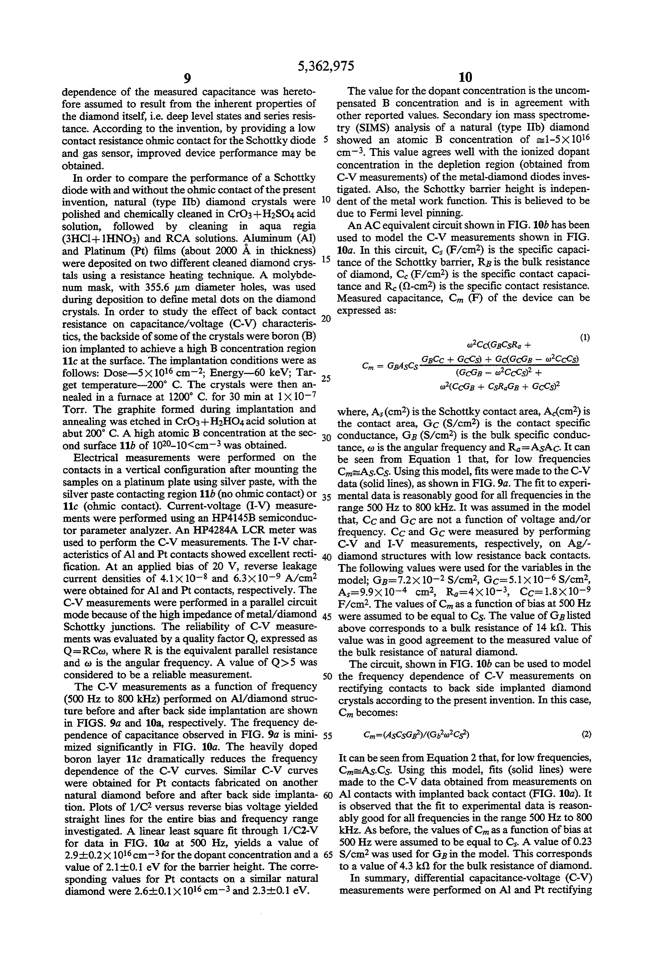
dependence of the measured capacitance was hereto The value for the dopant concentration is the uncom fore assumed to result from the inherent properties of pensated B concentration and is in agreement with the diamond itself, i.e. deep level states and series resis other reported values. Secondary ion mass spectrome tance. According to the invention, by providing a low try (SIMS) analysis of a natural (type IIb) diamond contact resistance ohmic contact for the Schottky diode 5 showed an atomic B concentration of as 1-5X10¹⁶ and gas sensor, improved device performance may be cm3. This value agrees well with the ionized dopant obtained. concentration in the depletion region (obtained from In order to compare the performance of a Schottky C-V measurements) of the metal-diamond diodes inves diode with and without the ohmic contact of the present tigated. Also, the Schottky barrier height is indepen invention, natural (type IIb) diamond crystals were O dent of the metal work function. This is believed to be polished and chemically cleaned in CrO3--H2SO4 acid due to Fermi level pinning.
solution, followed by cleaning in aqua regia An AC equivalent circuit shown in FIG.10b has been (3HC1--1HNO3) and RCA solutions. Aluminum (Al) used to model the C-V measurements shown in FIG. and Platinum (Pt) films (about 2000 A in thickness) 10a. In this circuit, C.s (F/cm2) is the specific capaci were deposited on two different cleaned diamond crys 15 tance of the Schottky barrier, RB is the bulk resistance tals using a resistance heating technique. A molybde of diamond, Co (F/cm) is the specific contact capaci num mask, with 355.6 pum diameter holes, was used tance and Re (S)-cm) is the specific contact resistance. during deposition to define metal dots on the diamond Measured capacitance, Cn (F) of the device can be crystals. In order to study the effect of back contact 20 expressed as:
resistance on capacitance/voltage (C-V) characteris tics, the backside of some of the crystals were boron (B) occ(GBCsRa + (1) ion implanted to achieve a high B concentration region 11c at the surface. The implantation conditions were as Cn = GibASCs
GBCC -- GoCs) + Gc(GcGB - occCs) follows: Dose-5X1016 cm-2; Energy-60 keV; Tar 25 (GcGB - occCs) -- get temperature-200 C. The crystals were then an o(CCGB -- CsRGB + GoCs)? nealed in a furnace at 1200° C. for 30 min at 1 x 10⁻⁷
Torr. The graphite formed during implantation and where, As (cm2) is the Schottky contact area, A(cm2) is annealing was etched in CrO3--H2HO4 acid solution at the contact area, Gc (S/cm2) is the contact specific abut 200° C. A high atomic B concentration at the sec 30 conductance, GB (S/cm2) is the bulk specific conduc ond surface 11b of 1020-10<cm-3 was obtained. tance, c) is the angular frequency and Ra=ASAC. It can Electrical measurements were performed on the be seen from Equation 1 that, for low frequencies contacts in a vertical configuration after mounting the Cns A.S.C.S. Using this model, fits were made to the C-V samples on a platinum plate using silver paste, with the data (solid lines), as shown in FIG. 9a. The fit to experi silver paste contacting region 11b (no ohmic contact) or 35 mental data is reasonably good for all frequencies in the 11c (ohmic contact). Current-voltage (I-V) measure range 500 Hz to 800 kHz. It was assumed in the model ments were performed using an HP4145B semiconduc that, CC and GC are not a function of voltage and/or tor parameter analyzer. An HP4284A LCR meter was frequency. CC and GC were measured by performing used to perform the C-V measurements. The I-V char C-V and I-V measurements, respectively, on Ag/- acteristics of Al and Pt contacts showed excellent recti diamond structures with low resistance back contacts. fication. At an applied bias of 20 V, reverse leakage The following values were used for the variables in the current densities of 4.1 x 10⁻⁸ and 6.3X 10⁻⁹ A/cm2 model; GB=7.2x10⁻² S/cm2, GC=5.1X 10⁻⁶ S/cm2, were obtained for Al and Pt contacts, respectively. The As=9.9x10⁻⁴ cm2, R=4x10⁻³, CC= 1.8x10⁻⁹ C-V measurements were performed in a parallel circuit F/cm2. The values of Cn as a function of bias at 500 Hz mode because of the high impedance of metal/diamond 45 were assumed to be equal to Cs. The value of GB listed Schottky junctions. The reliability of C-V measure above corresponds to a bulk resistance of 14 k(). This ments was evaluated by a quality factor Q, expressed as value was in good agreement to the measured value of Q=RCo), where R is the equivalent parallel resistance the bulk resistance of natural diamond. and c) is the angular frequency. A value of Q25 was The circuit, shown in FIG. 10b can be used to model considered to be a reliable measurement. 50 the frequency dependence of C-V measurements on The C-V measurements as a function of frequency rectifying contacts to back side implanted diamond (500 Hz to 800 kHz) performed on Al/diamond struc crystals according to the present invention. In this case, ture before and after back side implantation are shown Cn becomes:
in FIGS. 9a and 10a, respectively. The frequency de pendence of capacitance observed in FIG. 9a is mini 55 Cn=(AsCSGs)/(GoCs) (2) mized significantly in FIG. 10a. The heavily doped boron layer 11c dramatically reduces the frequency It can be seen from Equation 2 that, for low frequencies, dependence of the C-V curves. Similar C-V curves CnsAS.Cs. Using this model, fits (solid lines) were were obtained for Pt contacts fabricated on another made to the C-V data obtained from measurements on natural diamond before and after back side implanta Al contacts with implanted back contact (FIG. 10a). It tion. Plots of 1/C2 versus reverse bias voltage yielded is observed that the fit to experimental data is reason straight lines for the entire bias and frequency range ably good for all frequencies in the range 500 Hz to 800 investigated. A linear least square fit through 1/C2-V kHz. As before, the values of Cn as a function of bias at for data in FIG. 10a at 500 Hz, yields a value of 500 Hz were assumed to be equal to C. A value of 0.23 2.9-0.2x 1016 cm-3 for the dopant concentration and a 65 S/cm2 was used for GB in the model. This corresponds value of 2.1-0.1 eV for the barrier height. The corre to a value of 4.3 kg) for the bulk resistance of diamond. sponding values for Pt contacts on a similar natural In summary, differential capacitance-voltage (C-V) diamond were 2.6-0.1 x 1016 cm-3 and 2.3-0.1 eV. measurements were performed on Al and Pt rectifying
Page 22
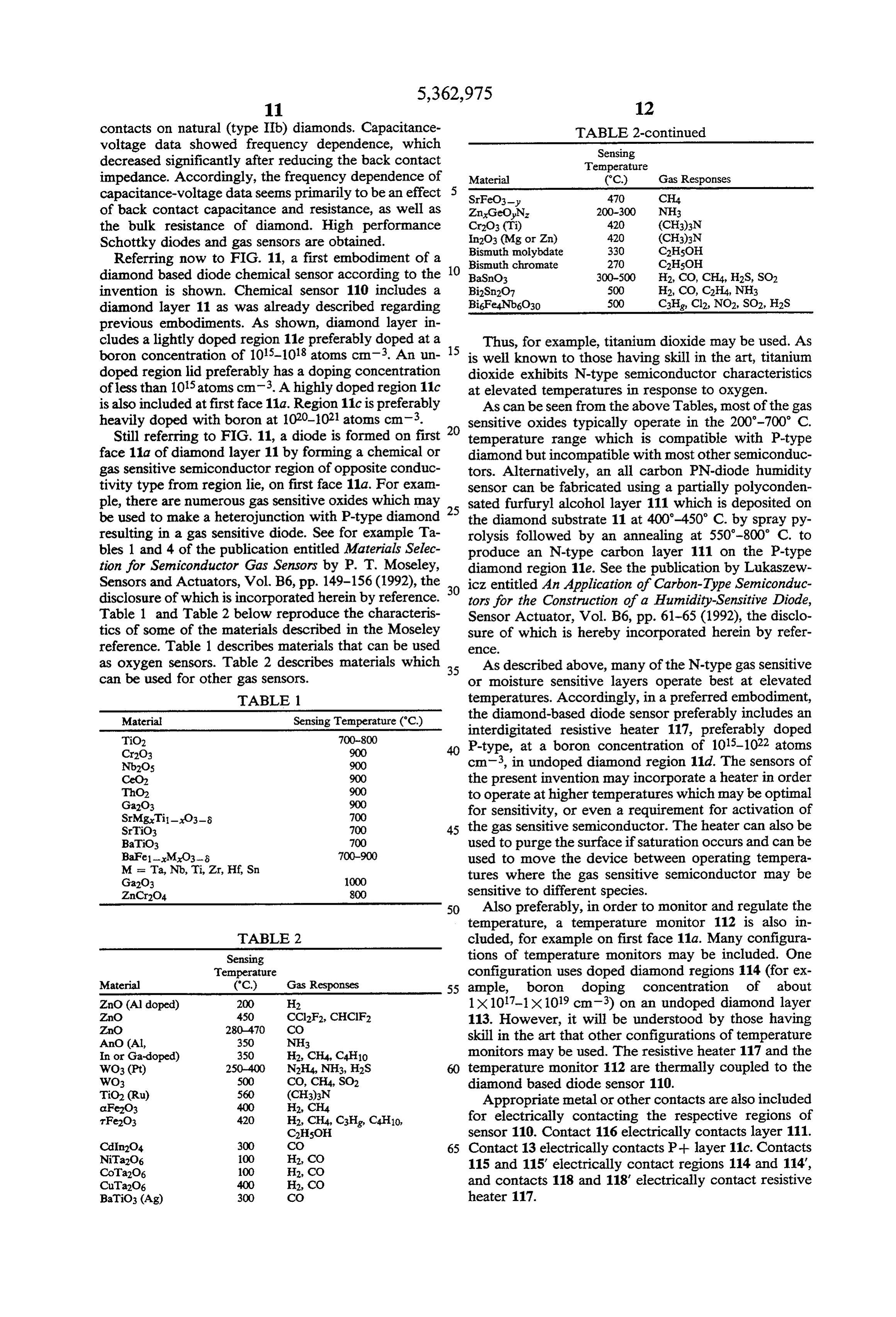
contacts on natural (type IIb) diamonds. Capacitance TABLE 2-continued voltage data showed frequency dependence, which Sensing decreased significantly after reducing the back contact Temperature impedance. Accordingly, the frequency dependence of Material (°C) Gas Responses capacitance-voltage data seems primarily to be an effect 5 SrFeO3-y 470 CH4 of back contact capacitance and resistance, as well as ZnxGeON 200-300 NH3 the bulk resistance of diamond. High performance Cr2O3 (T) 420 (CH3)3N Schottky diodes and gas sensors are obtained. In2O3 (Mg or Zn) 420 (CH3)3N Referring now to FIG. 11, a first embodiment of a Bismuth molybdate
Bismuth chromate
diamond based diode chemical sensor according to the BaSnO3 10
invention is shown. Chemical sensor 110 includes a Bi2Sn2O7 500 H2, CO, C2H4, NH3 diamond layer 11 as was already described regarding BigFeNb6O30 500 C3H Cl2, NO2, SO2, H2S previous embodiments. As shown, diamond layer in cludes a lightly doped region 11e preferably doped at a Thus, for example, titanium dioxide may be used. As boron concentration of 1015-1018 atoms cm-3. An un 15 is well known to those having skill in the art, titanium doped region lid preferably has a doping concentration dioxide exhibits N-type semiconductor characteristics of less than 1015 atoms cm3. A highly doped region 11c at elevated temperatures in response to oxygen. is also included at first face 11a. Region 11c is preferably As can be seen from the above Tables, most of the gas heavily doped with boron at 1020-1021 atoms cm-3. 20 sensitive oxides typically operate in the 200-700 C. Still referring to FIG. 11, a diode is formed on first temperature range which is compatible with P-type face 11a of diamond layer 11 by forming a chemical or diamond but incompatible with most other semiconduc gas sensitive semiconductor region of opposite conduc tors. Alternatively, an all carbon PN-diode humidity tivity type from region lie, on first face 11a. For exam sensor can be fabricated using a partially polyconden ple, there are numerous gas sensitive oxides which may sated furfuryl alcohol layer 111 which is deposited on be used to make a heterojunction with P-type diamond 25 the diamond substrate 11 at 400-450° C. by spray py resulting in a gas sensitive diode. See for example Ta rolysis followed by an annealing at 550-800° C. to bles 1 and 4 of the publication entitled Materials Selec produce an N-type carbon layer 111 on the P-type tion for Semiconductor Gas Sensors by P. T. Moseley, diamond region 11e. See the publication by Lukaszew Sensors and Actuators, Vol. B6, pp. 149-156 (1992), the icz entitled An Application of Carbon-Type Semiconduc disclosure of which is incorporated herein by reference. 30 tors for the Construction of a Humidity-Sensitive Diode, Table 1 and Table 2 below reproduce the characteris Sensor Actuator, Vol. B6, pp. 61-65 (1992), the disclo tics of some of the materials described in the Moseley sure of which is hereby incorporated herein by refer reference. Table 1 describes materials that can be used eCe.
as oxygen sensors. Table 2 describes materials which 35 As described above, many of the N-type gas sensitive can be used for other gas sensors. or moisture sensitive layers operate best at elevated TABLE 1 temperatures. Accordingly, in a preferred embodiment,
Material Sensing Temperature (C.) the diamond-based diode sensor preferably includes an
interdigitated resistive heater 117, preferably doped
Cr2O3 900 P-type, at a boron concentration of 1015-1022 atoms Nb2O5 900 cm3, in undoped diamond region 11d. The sensors of CeO2 900 the present invention may incorporate a heater in order Tho2 900 to operate at higher temperatures which may be optimal Ga2O3 900 for sensitivity, or even a requirement for activation of
SrTiO3 700 45 the gas sensitive semiconductor. The heater can also be BaTiO3 700 used to purge the surface if saturation occurs and can be
700-900 used to move the device between operating tempera
Ga2O3 1000 tures where the gas sensitive semiconductor may be ZnCr2O4 800 sensitive to different species.
50 Also preferably, in order to monitor and regulate the temperature, a temperature monitor 112 is also in
TABLE 2. cluded, for example on first face 11a. Many configura
Sensing tions of temperature monitors may be included. One
Temperature configuration uses doped diamond regions 114 (for ex Material ("C) Gas Responses 55 ample, boron doping concentration of about ZnO (Al doped) 200 H2 1x10¹⁷-1X 1019 cm-3) on an undoped diamond layer ZnO
ZnO
113. However, it will be understood by those having
AnO (Al, 350 NH3 skill in the art that other configurations of temperature In or Ga-doped) 350 H2, CH4, C4H10 monitors may be used. The resistive heater 117 and the WO3 (Pt) 250-400 N2H4, NH3, H2S temperature monitor 112 are thermally coupled to the WO3 500 CO, CH4, SO2 diamond based diode sensor 110. TiO2 (Ru) 560 (CH3)3N Appropriate metal or other contacts are also included
TFe2O3 420 H2, CH4, C3Hg., C4H10, for electrically contacting the respective regions of C2H5OH sensor 110. Contact 116 electrically contacts layer 111.
CdIn2O4. 300 CO 65 Contact 13 electrically contacts P-- layer 11c. Contacts NiTa2O6 100 H2, CO 115 and 115 electrically contact regions 114 and 114",
CuTa2O6 400 H2, CO and contacts 118 and 118' electrically contact resistive BaTiO3 (Ag) 300 CO heater 117.
Page 23
Finally, appropriate external connections are pro FIG. 22 illustrates a Schottky diode chemical sensor vided for the device. In particular, a cathode C, an according to the present invention. As shown, sensor anode A, a pair of temperature monitor connections T, 220 is similar to sensor 10 of FIG. 1 except a tempera T', and a pair of heater connections H, H' are provided. ture monitor 112 and interdigitated resistive heater 117 The device is also encapsulated by layer 17 as was al have been added. The temperature monitor and resis ready described in connection with previous embodi tive heater allow the Schottky diode to operate at an ments. However, it will be understood by those having elevated temperature above ambient temperature. skill in the art that the use of diamond in the sensor may It will be understood by those having skill in the art reduce or eliminate the need for encapsulation. that a relatively thick insulating layer 21 may be used to FIG. 12 illustrates a second embodiment of a diode 10 form an MOS capacitor rather than a Schottky diode. based diamond chemical sensor. As shown, chemical For example, an insulating layer between 1000-2000 A sensor 120 includes a buried anode contact 13 with P thick may be used to forman MOS capacitor. It will be layer 11c adjacent thereto. The remaining structure is understood by those having skill in the art that the similar to that described in FIG. 11. FIG. 13 illustrates capacitance of the MOS capacitor changes similar to a third embodiment of a diode based chemical sensor 15 that of the Schottky diode in response to changes in gas 130 in which the resistive heater 117 is at face 11a and concentration. Either the metal gate 12 or the insulator the anode contact is at face 11b. The device is mounted 21 may be formed of a gas sensitive material which on a substrate 131 such as a metal substrate. affect the capacitance measurements performed on the FIG. 14 illustrates a fourth embodiment of a diode 20 device. For example, a catalytic metal such as platinum based sensor 140. As shown, anode contact 13 and P may be used for layer 21 as described for example in layer 11c are formed within an aperture 19 of a substrate Lundström et al., Physics With Catalytic Metal Gate 18 as was already described in connection with FIG. 5. Chemical Sensors, CRC Critical Reviews in Solid State FIG. 15 illustrates a fifth embodiment of a diamond and Materials Sciences, Vol. 15, Issue 3, pp. 201-278 based diode chemical sensor. This sensor 150 is sensitive 25 (1989), the disclosure of which is hereby incorporated to chemicals in a liquid 151. The liquid is contained herein by reference.
adjacent N-layer 111 by a membrane 152. Operation of the sensors described in FIGS. 11-22 Referring now to FIG.16, a diamond-based transistor will now be described. By providing a highly doped chemical sensor is illustrated. As shown, sensor 160 is region 11c, 11c' which provides a low resistance ohmic similar to sensor 110 (FIG. 11) except that a field effect 30 contact for anode 13, source 161, and drain 162, the transistor rather than a diode is provided. In order to frequency dependence of the measured capacitance can implement the field effect transistor, a pair of P-- re be significantly reduced or even eliminated. Thus the gions 11c, 11c' are provided. A source contact and a frequency dependence of the capacitance/voltage char drain contact 161, 162 respectively, are provided, and acteristics is reduced significantly. Moreover, by pro source and drain connections S and D respectively, are 35 viding diamond-based diode and transistor sensors, high also provided. An insulating layer 163 such as silicon sensitivity may be achieved at high temperatures. The dioxide or insulating diamond is provided along with a interdigitated resistive heater 117 can be used to main gate contact 164 which may be a catalytic metal such as tain the device at elevated temperatures such as be palladium. A gate connection G is also provided. tween 300-700 C., for optimal sensitivity, and the FIG. 17 illustrates a second embodiment of a dia temperature monitor 112 can be used to monitor the mond-based transistor chemical sensor. Sensor 170 is sensor temperature.
similar to sensor 150 (FIG. 15), except that source and Thus, the inherent advantages of diamond compared drain contacts 161 and 162 respectively are buried to silicon or gallium arsenide as a semiconductor can be within diamond layer 11. FIG. 18 illustrates a third exploited in the chemical sensors of the present inven embodiment of a diamond-based transistor chemical 45 tion, to provide high temperature, high speed and high sensor. Sensor 180 is similar to sensor 170 (FIG. 17), power chemical sensors. Moreover, chemical sensors except that source and drain contacts 161, 161' are are the most difficult sensors to encapsulate and inte formed on face 11b of layer 11. FIG. 19 illustrates a grate into state-of-the-art electronics because of the fourth embodiment of a diamond-based transistor chem harsh environments in which they operate. Utilization ical sensor. Sensor 190 is similar to sensor 180 (FIG. 18), 50 of diamond as a chemical sensing semiconductor may except source and drain contacts 161, 161' are formed in reduce the need to encapsulate the device because of an aperture 19 in substrate 18. FIG. 20 illustrates fifth diamond's inherent chemical robustness. embodiment of a diamond-based transistor chemical In fabricating diodes or transistors as shown in FIGS. sensor. Sensor 200 is similar to sensor 160 (FIG.16), 11-22, it will be understood that either the insulating except that a membrane 152 is added for detection of 55 layer 163, 21 or the cathode/gate contact 164, 12 or ionic species in the liquid 151. both, can be the sensing material. For example, plati FIG. 21 illustrates a sixth embodiment of a diamond num on silicon dioxide on P-type diamond acts as a based transistor chemical sensor. Sensor 210 is similar to hydrogen sensor. While not wishing to be bound by any sensor 200 (FIG. 20) except that a reference electrode theory, it is hypothesized that hydrogen molecules or 241, which is spaced apart from insulating layer 163, is 60 atoms absorb on the metal surface and change the sur used. This configuration of an insulating layer and a face potential of the metal, resulting in a shift of a spaced apart reference electrode with an electrolyte capacitance/voltage (C-V) curve relative to the mea solution 151 therebetween is similar to the configuration surement in the absence of hydrogen. However, any described in a publication entitled Hydrogeninated change in the insulator or metal gate due to an adsorbed Amorphous Silicon Technology for Chemically Sensitive 65 or absorbed gas will affect the C-V curve. A typical Thin-Filmed Transistors by Mariucci et al., Sensors and C-V curve is illustrated in FIG. 23. Accordingly, the Actuators, Vol. B6, pp. 29-33 (1992), the disclosure of choice of insulator or metal gate may vary depending which is hereby incorporated herein by reference. upon the chemical to be sensed.
Page 24
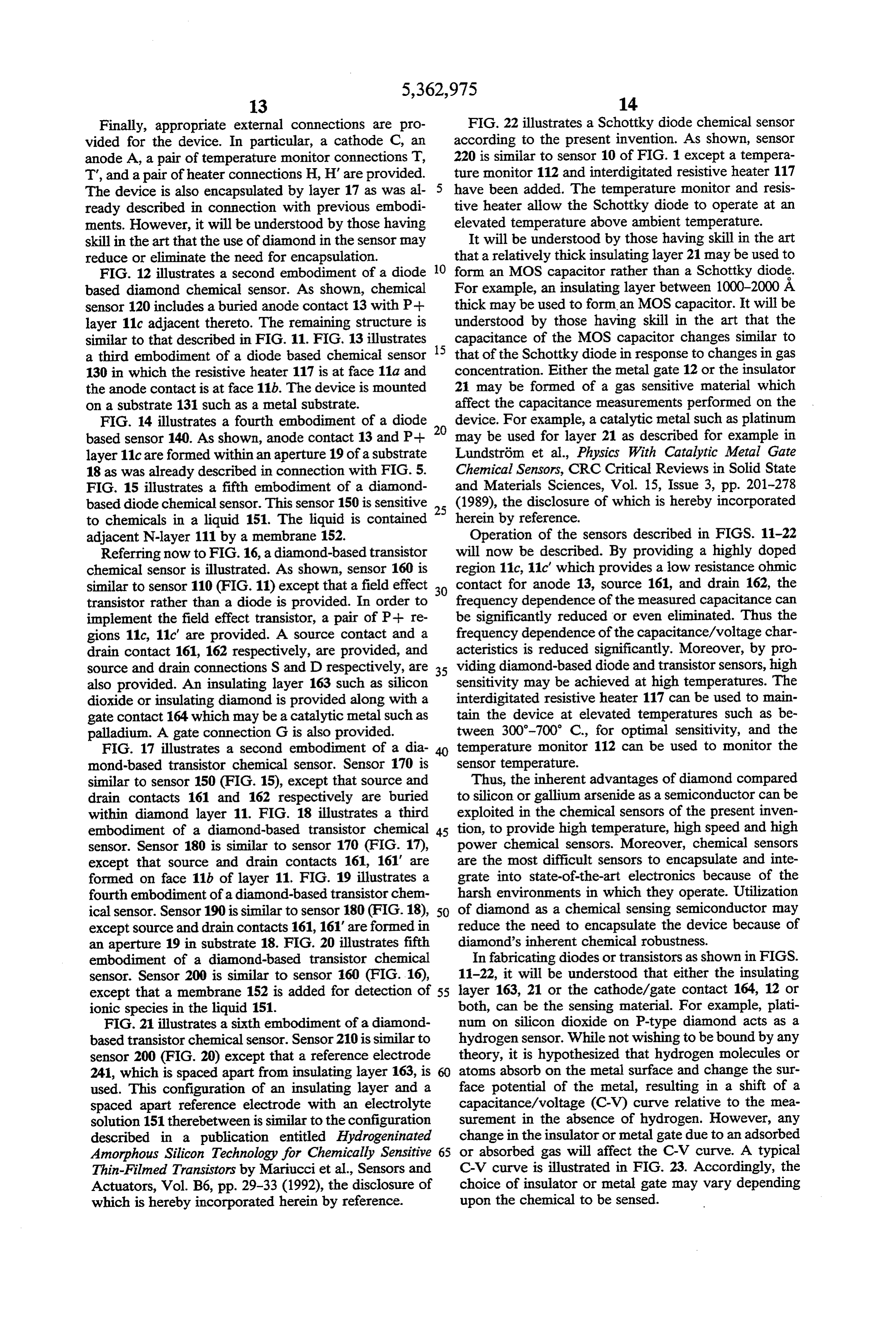
In designing a P-N chemical sensitive diode, many layer, and wherein said heating means comprises a resis gas sensitive oxides may be used to make a heterojunc tive heater in said undoped diamond layer. tion with P-type diamond, resulting in a gas sensitive 9. The diamond-based chemical sensor of claim 7 diode. As discussed above for a field effect transistor/- further comprising means, thermally coupled to at least capacitor structure, any modification of the gas sensi 5 one of said first and second layers, for monitoring the tive material in the device will affect the capacitance temperature of said diamond-based chemical sensor. voltage curve. Additionally, the presence of the gas 10. The diamond-based chemical sensor of claim 1 should be apparent in current-voltage (I-V) measure further comprising means for confining a chemical con ments for a field effect transistor. The expected current taining liquid adjacent one of said first and second lay or voltage response of a field effect transistor is illus O S.11. The diamond-based chemical sensor of claim 1 trated in FIG. 24 which is a plot of drain current versus gate voltage for constant source and drain voltage. further comprising:
In the drawings and specification, there have been a substrate on said first diamond layer opposite said disclosed typical preferred embodiments of the inven second semiconductor layer, said substrate having tion and, although specific terms are employed, they are 15 an aperture therein for exposing said first diamond used in a generic and descriptive sense only and not for layer;
purposes of limitation, the scope of the invention being an electrical contact on said first diamond layer in set forth in the following claims. said aperture; and
That which is claimed is: a region of said first conductivity type in said first 1. A diamond-based chemical sensor comprising: 20 diamond layer, adjacent said electrical contact and a first diamond layer having a first conductivity type; which is highly doped relative to said first diamond a second semiconductor layer of a second conductiv layer, such that said electrical contact forms an ity type on said first diamond layer, said first and ohmic contact with said region. second layers forming a semiconductor junction 25 12. A diamond-based chemical sensor comprising: therebetween; a diamond layer;
at least one of said first and second layers being con a transistor in said diamond layer, said transistor in figured to allow a chemical external to said dia cluding a controlling electrode, a first controlled mond-based chemical sensor to interact with said at electrode and a second controlled electrode; said controlling electrode being configured to allow a least one of said first and second layers and alter an 30 chemical external to said diamond-based chemical electrical characteristic of said semiconductor sensor to interact with said controlling electrode junction. and alter an electrical characteristic of said transis 2. The diamond-based chemical sensor of claim 1 tor.
wherein said first diamond layer is a P-type diamond 13. The diamond-based chemical sensor of claim 12 layer and wherein said second semiconductor layer is 35 wherein said transistor is a field effect transistor, selected from the group consisting of an N-type gas wherein said controlling electrode is a gate electrode, sensitive second diamond layer, an N-type moisture wherein said first controlled electrode is a source elec sensitive second semiconductor layer, an N-type gas trode and wherein said second controlling electrode is a sensitive semiconducting oxide layer and an N-type drain electrode.
carbon layer. 14. The diamond-based chemical sensor of claim 13 3. The diamond-based chemical sensor of claim 1 wherein said gate electrode comprises an insulating further comprising: layer on said diamond layer and a gate contact on said an electrical contact on said first diamond layer; and gate insulating layer, opposite said diamond layer, at a region of said first conductivity type in said first least one of said insulating layer and said gate contact diamond layer, adjacent said electrical contact and 45 being selected to allow a chemical external to said dia which is highly doped relative to said first diamond mond-based chemical sensor to interact therewith, and layer, such that said electrical contact forms an alter the characteristics of said field effect transistor. ohmic contact with said region. 15. The diamond-based chemical sensor of claim 12 4. The diamond-based chemical sensor of claim 3 wherein said first controlled electrode includes a first wherein said electrical contact is on said first diamond 50 electrical contact on said diamond layer and a first re layer opposite said second semiconductor layer, said gion adjacent said first electrical contact and which is diamond-based chemical sensor further comprising a highly doped relative to said diamond layer, such that substrate on said first diamond layer, opposite said sec said first electrical contact forms a first ohmic contact ond semiconductor layer, and surrounding said electri with said first region; and wherein said second con cal contact. 55 trolled electrode includes a second electrical contact on 5. The diamond-based chemical sensor of claim 4 said diamond layer and a second region adjacent said further comprising heating means in said substrate, for second electrical contact and which is highly doped heating said diamond sensor above an ambient tempera relative to said diamond layer, such that said second ture. electrical contact forms a second ohmic contact with 6. The diamond-based chemical sensor of claim 5 said second region.
wherein said substrate is an undoped diamond substrate. 16. The diamond-based chemical sensor of claim 13 7. The diamond-based chemical sensor of claim 1 wherein said source, drain and gate electrodes are further comprising means, thermally coupled to at least formed on a first face of said diamond layer. one of said first and second layers, for heating said 17. The diamond-based chemical sensor of claim 13 diamond sensor above an ambient temperature. 65 wherein said gate electrode is formed on a first face of 8. The diamond-based chemical sensor of claim 7 said diamond layer and wherein said source electrode further comprising an undoped diamond layer on said and said drain electrode are formed on a second face of first diamond layer, opposite said second semiconductor said diamond layer.
Page 25
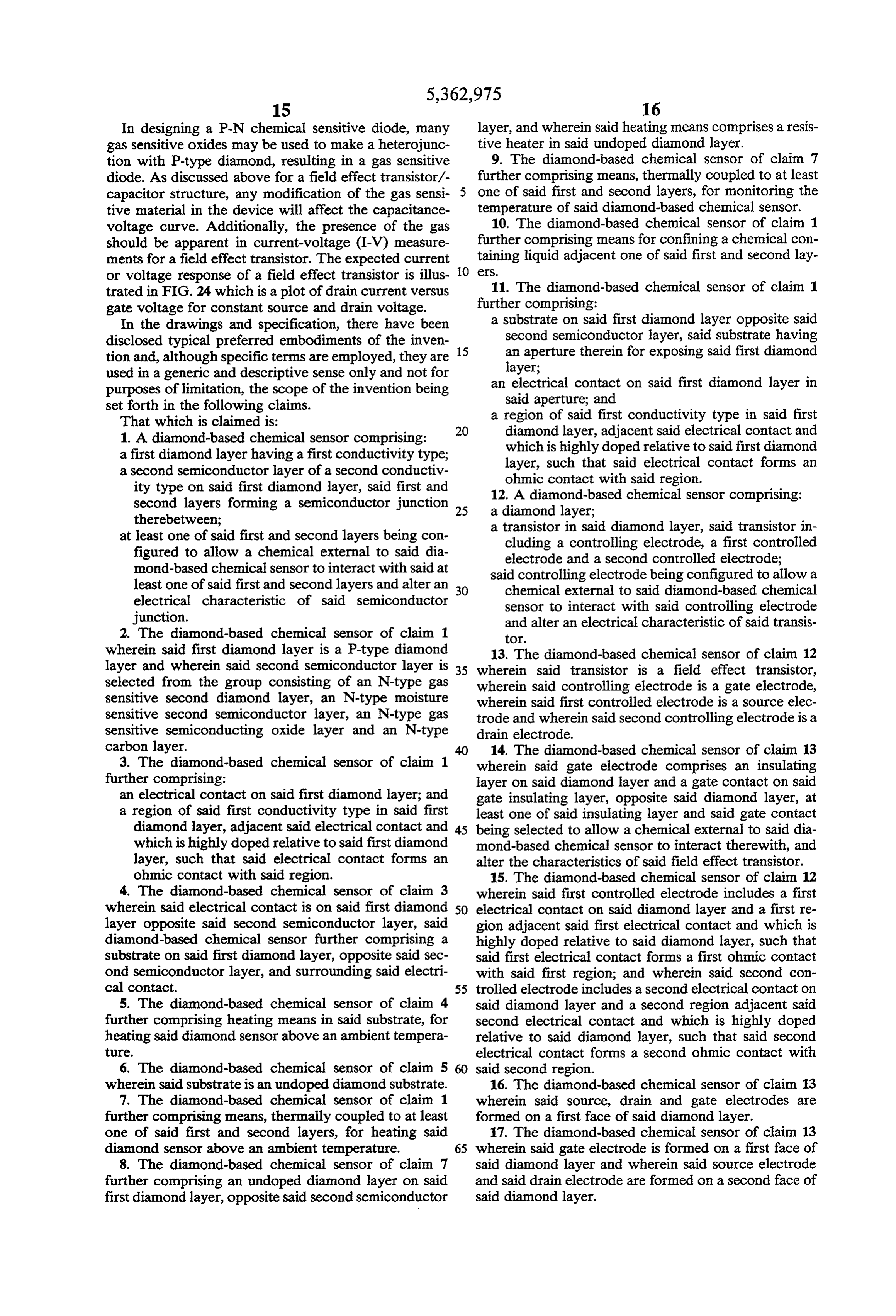
18. The diamond-based chemical sensor of claim 16 27. The diamond-based chemical sensor of claim 12 further comprising a substrate on said diamond layer, further comprising means for confining a chemical con opposite said source, drain and gate electrodes. taining liquid adjacent said gate electrode. 19. The diamond-based chemical sensor of claim 18 28. The diamond-based chemical sensor of claim 27 further comprising heating means in said substrate, for wherein said gate electrode is spaced apart from said heating said diamond sensor above an ambient tempera insulating layer, and wherein said confining means con ture.
fines said chemical containing liquid between said gate 20. The diamond-based chemical sensor of claim. 19 electrode and said insulating layer.
29. A diamond-based chemical sensor comprising:
wherein said substrate is an undoped diamond substrate. a diamond layer;
21. The diamond-based chemical sensor of claim 17 a chemically sensitive layer on said diamond layer; further comprising a substrate on said second face, and heating means, thermally coupled to said diamond surrounding said source and drain electrodes. layer, for heating said diamond-based chemical 22. The diamond-based chemical sensor of claim 21 sensor above an ambient temperature; and further comprising heating means in said substrate, for 15 temperature monitoring means, thermally coupled to heating said diamond sensor above an ambient tempera said diamond layer, for monitoring the temperature tre. of said diamond-based chemical sensor. 23. The diamond-based chemical sensor of claim 22 30. The diamond-based chemical sensor of claim 29 wherein said substrate is an undoped diamond substrate. 20 wherein said heating means is a resistive heating means 24. The diamond-based chemical sensor of claim 12 in said diamond layer.
31. The diamond-based chemical sensor of claim 29 further comprising means, thermally coupled to at least wherein one of said diamond layer, for heating said diamond said temperature monitoring means includes at based sensor above an ambient temperature. least a second diamond layer on said diamond layer. 32. The diamond-based chemical sensor of claim 30 25. The diamond-based chemical sensor of claim 24 25 wherein said temperature monitoring means includes at further comprising an undoped second diamond layer least a second diamond layer on said diamond layer. on said first diamond layer, opposite said gate electrode, 33. The diamond-based chemical sensor of claim 29 and wherein said heating means comprises a resistive further comprising at least one electrode, said at least heater in said undoped second diamond layer. one electrode in combination with at least said diamond 26. The diamond-based chemical sensor of claim 24 layer and said chemically sensitive layer forming one of further comprising means, thermally coupled to at least a junction diode, a Schottky diode, a capacitor and a one of said first and second layers, for monitoring the transistor.
temperature of said diamond-based chemical sensor.
Provenance
- Collection
- Cited prior art
- Original PDF
- patentimages.storage.googleapis.com →
- Filed
- 1993-07-08
- Pages
- 25
- Method
- pdftotext (the PDF's own text layer) + pdftoppm 300dpi page scans
- Source
- Google Patents bibliographic record
- Granted
- 1994-11-08
- Inventors
- Jesko von Windheim; Vasudev Venkatesan; Kobe Steel USA Inc
- Transcribed from
- patentimages.storage.googleapis.com →