patent · US4793910
Multielectrode photoelectrochemical cell for unassisted photocatalysis and photosynthesis
27 December 1988
Page 1 — bibliographic record
United States Patent (19) 11 Patent Number: 4.793,910 Smotkin et al. (45) Date of Patent: Dec. 27, 1988 (54) MULTELECTRODE 4,357,400 ll/1982 Appleby .............................. 429/11 PHOTOELECTROCHEMICAL CELL FOR 4,368,216 1/1983 Manassen et al. ... ... 429/11 X UNASSISTED PHOTOCATALYSIS AND E. A3 WiNRA w w w - - - - - - 429/111
PHOTOSYNTHESIS 4,419,278 12/1983 Gordon ........................... 429/11 X (75) Inventors: Eugene Smotkin; Allen J. Bard; 4,437,954 3/1984 Sammells et al. ................... 204/129 Marye A. Fox, all of Austin, Tex. 4,466,869 8/1984 Ayers ................... ... 204/129
(73) Assignee: Gas Research Institute, Chicago, Ill. 4,501,804 2/1985 Bockris et al. ... ... 429/11 (21) Appl. No.: 51,469 4,521,499 6/1985 Switzer ............ ... 429/11
22 Filed: May 18, 1987 4,534,099 9/1985 Howe .................................... 29/572 4,592,807 6/1986 Switzer ................................ 204/2.1 (51) Int. Cl* .......................... C25B 1/04; C25B 9/04;
(52) U.S. C. .................................... 20/268; 20/270; Honda et al., Nature, 238:37 (1972).
58) Field of Search ............... 204/129, 268, 269, 270,
20/DIG. 3, 28, 29/11 smokinet al., J. of Phys. Chem. 91.6 (Jan.14, 1987).
References Cited Dialog and Lexis search.
4,021,323 5/1977 Kilby et al. ......................... 204/129 Primary Examiner-Donald R. Valentine 4,042,758 8/1977 Weinstein et al. .................. 429/111 Attorney, Agent, or Firm-Arnold, White & Durkee 4,061,555 12/1977. Miyatani et al. .................... 204/242 4,090,933 33; M.A. alm E (57) ABSTRACT 4,094,751 6/1978 Nozik et al..... 20/29X A multielectrode photoelectrochemical cell in which at E. A. S.O.E. produce
4,136,436 1/1979 Kilby et al. ........................... 29/572
H2O2 without external bias. In one embodi electrochemical reactions such as water photolysis to 4,167,461 9/1979 Dickson et al. ..................... 204/102 ment of the present invention, a bipolar TiO2/Pt multi 4,181,593 1/1980 McKinzie et al. .............. 204/290 F electrode photoelectrochemical cell was fabricated 4,181,754 1/1980 McKinzie et al. .................... 427/7 with five panels in series. The cell permitted unassisted 4,203,814 5/1980 Granthan ........................... 204/129 photolytic (Xe lamp) water splitting to produce H2 and 4,215, 182 7/1980 Ang et al. ............................. 429/15 O2 with H2O 1 tio of 2.4/l 4,236,984 12/1980 Grantham ........................... 204/129 2 with H2O2 molar ratio of 2.4/l.
4,288,502 9/1981 Avigal et al. ....................... 429/11 4,315,973 2/1982 Manassen et al. .............. 204/275 X 23 Claims, 8 Drawing Sheets
SA-S-A-S-N-SA-AA-S-N SLS
Page 2
Drawing sheet — no readable text.
Page 3
Drawing sheet — no readable text.
Page 4
Drawing sheet — no readable text.
Page 5
Drawing sheet — no readable text.
Page 6
Drawing sheet — no readable text.
Page 7
Drawing sheet — no readable text.
Page 8
Drawing sheet — no readable text.
Page 9
Drawing sheet — no readable text.
Page 10
photolysis of water into H2 and O2 using light from, for
MULTELECTRODE example, solar radiation.
PHOTOELECTROCHEMICAL CELL FOR
UNASSISTED PHOTOCATALYSS AND SUMMARY OF THE INVENTION
PHOTOSYNTHESIS The present invention involves a multielectrode photoelectrochemical unit for unassisted photoelectri
BACKGROUND OF THE INVENTION cally-induced reactions. The photoelectrically-induced The present invention relates to photolytically reaction of most general interest is the decomposition of induced decompositions such as water photoelectrol 10 water to hydrogen and oxygen, however many other ysis, particularly with a multielectrode semiconductor photodriven reactions (e.g. that of brine to produce photoelectrochemical cell capable of unassisted photo hydrogen, chlorine, and alkali can be carried out. In lytic water splitting to form H2 and O2 and methods of one aspect the multielectrode photoelectrochemical making and using same. The present invention does not unit comprises a wireless series of at least two photoac require that the semiconductor have a flatband potential 15 tive bipolar electrode panels. The multielectrode photo more negative than the reduction potential of H2O or electrochemical unit characteristically comprises a that the semiconductor be stable with respect to photo housing and at least two photoactive bipolar electrode oxidation while evolving oxygen. panels and may also include a means for collecting Photolytically induced decompositions, particularly evolved gaseous photodecomposition products. The the photolysis of water into H2 and O2 using solar radia housing has at least one light-passing side, a first end, a tion, have received extensive attention and various 20 second end and a housing wall defining an internal photoelectrochemical devices and methods for this section. The term "light-passing” as used herein indi purpose have been developed. However, in many cases, cates light-transparent or light-translucent, so that sub an expenditure of electrical or chemical energy in addi stantially all incident light may pass on into the housing tion to incident radiant (e.g., solar) energy is required. 25 interior.
Because the potential developed by a single photoelec A first exterior photoactive bipolar electrode panel is trode in these devices is inadequate to drive the water mounted in the internal section so that the first elec splitting reaction at a useful rate with visible light, an trode panel physically separates the internal section on external bias has been necessarily applied. This bias has each side of the first panel. Said first exterior photoac been either an external electrical potential or a chemical tive bipolar electrode panel has a semiconductor side, bias established by contacting semiconductor sides of an ohmic contact layer and an underside. This first bipolar photoelectrodes with a strong alkali and metal exterior photoactive bipolar electrode panel is attached lic sides with a strong acidic solution. Although it is to the housing wall near the first end of the internal known that connecting several photoactive junctions in section with the semiconductor side oriented toward series may generate sufficient driving force to decom 35 the first end and partially forming a first terminal com pose H2O to H2 and O2 without an external bias, there partment.
are still some problems related to earlier devices such as A second exterior photoactive bipolar electrode complicated construction or difficulties in the separa panel is mounted in the internal section so that the sec tion and collection of H2 and O2, thus impeding practi ond electrode panel physically separates the internal cal application. Examples of attempted practical photo 40 section on each side of the panel. Said exterior second electrochemical devices are seen in White et al., (J. photoactive bipolar electrode panel has a semiconduc Electrochem. Sol. Vol. 132, p 544 (1985)), and in U.S. tor side, an ohmic contact layer and a catalytic side and Pat. No. 4,094,751, issued June 13, 1978. being attached to the housing wall near the second end Studies of water photoelectrolysis ("water splitting') of the internal section with the catalytic side oriented with TiO2 and Pt electrodes date from the work of 45 toward the second end and partially forming a second Honda et al., (Nature, (1972), v. 238, pp. 37). Because terminal compartment.
the potential developed by platinized TiO2 is inadequate An internal compartment in said internal section is to drive the water splitting reaction at a useful rate, an partially formed by the catalytic side of the first exterior external bias must be applied. This bias can be either an photoactive bipolar electrode panel and the semicon external electrical potential or a chemical bias estab 50 ductor side of the exterior second photoactive bipolar lished by contacting the TiO2 with a strong alkaline and electrode panel. The first and second exterior photoac the Pt with a strong acidic solution. (Wrighton, Proc. tive bipolar electrode panels are attached to said hous Nat. Acad. Sci., (1975), U.S.A., V 72, pp. 1518). ing walls to prevent liquid flow between the internal In such cases an expenditure of energy in addition to compartment and the terminal compartments. The exte the incident radiant (e.g., solar) energy is required. An 55 rior photoactive bipolar electrode panels are positioned alternative strategy involves the utilization of one or in the internal section so that light from an external more PEC cells to bias the water splitting cell. Earlier source entering the internal section is substantially inci work (White et al., cited above) showed, for example, dent upon their semiconductor sides. The internal com that this could be accomplished by coupling of Texas partment preferably comprises a closable port in the Instruments solar energy system arrays based on Sip/n housing wall.
junctions. Simpler types of bipolar electrodes, and ar The semiconductor side of a usable photoactive bipo rays based on these, have not previously been de lar electrode panel of the present invention preferably scribed. comprises a p-type semiconductor or a n-type semicon A photoelectrochemical device which is of relatively ductor. The catalytic side of the photoactive bipolar simple construction, allowing ready collection of H2 65 electrode panels preferably comprises a catalyst such as and/or O2 and not requiring any external bias has not, platinum. The corresponding ohmic contact layer is a prior to the invention described herein, been developed thin electrically conductive substance, preferably a for photolytically-induced decompositions such as the metallic foil such as titanium foil.
Page 11
A preferred multielectrode photoelectrochemical means are emplaced to assure incidence of incoming unit for unassisted photodecomposition comprises at light on the photoactive semiconductor sides of the least two internal compartments and at least one interior panels.
photoactive bipolar electrode panel. The housing of an In a preferred embodiment, the interior photoactive interior photoactive bipolar electrode panel-containing bipolar electrode panel-containing multielectrode unit is generally as described above. photoelectrochemical unit of the present invention A first exterior bipolar electrode panel is attached to comprises means for the collection of gaseous photode the housing wall near the first end of the internal section composition products. Such means, of types well of the housing, said first exterior bipolar electrode panel known to those skilled in the art, are connected to or having a catalytic or gas-evolving side oriented toward 10 the first end of the housing and partially forming a first incorporated in at least one terminal compartment. terminal compartment. The first exterior bipolar elec chemical unit ofusetheofpresent
A preferred the multielectrode photoelectro invention is for the photo trode panel further comprises an ohmic contact layer voltaic decomposition of water to hydrogen and oxy and an internal side, and said first electrode panel ex gen powered by solar energy. For this use, the bipolar tends across the internal section to physically separate electrode panels may have an the ohmic contact layer the internal section on each side of the first electrode panel. comprising a metallic foil, a semiconductor side com prising a metal chalcogenide, an underside comprising
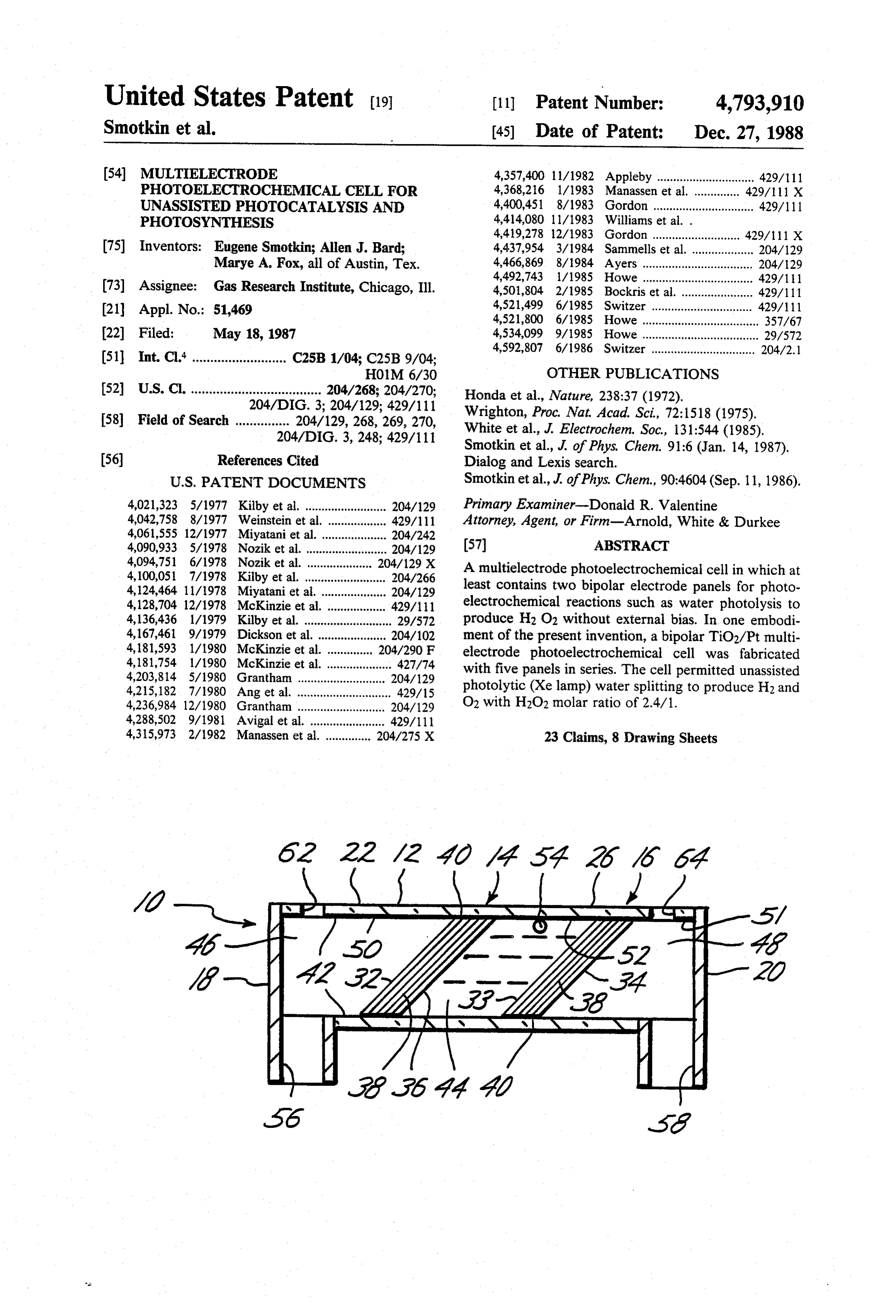
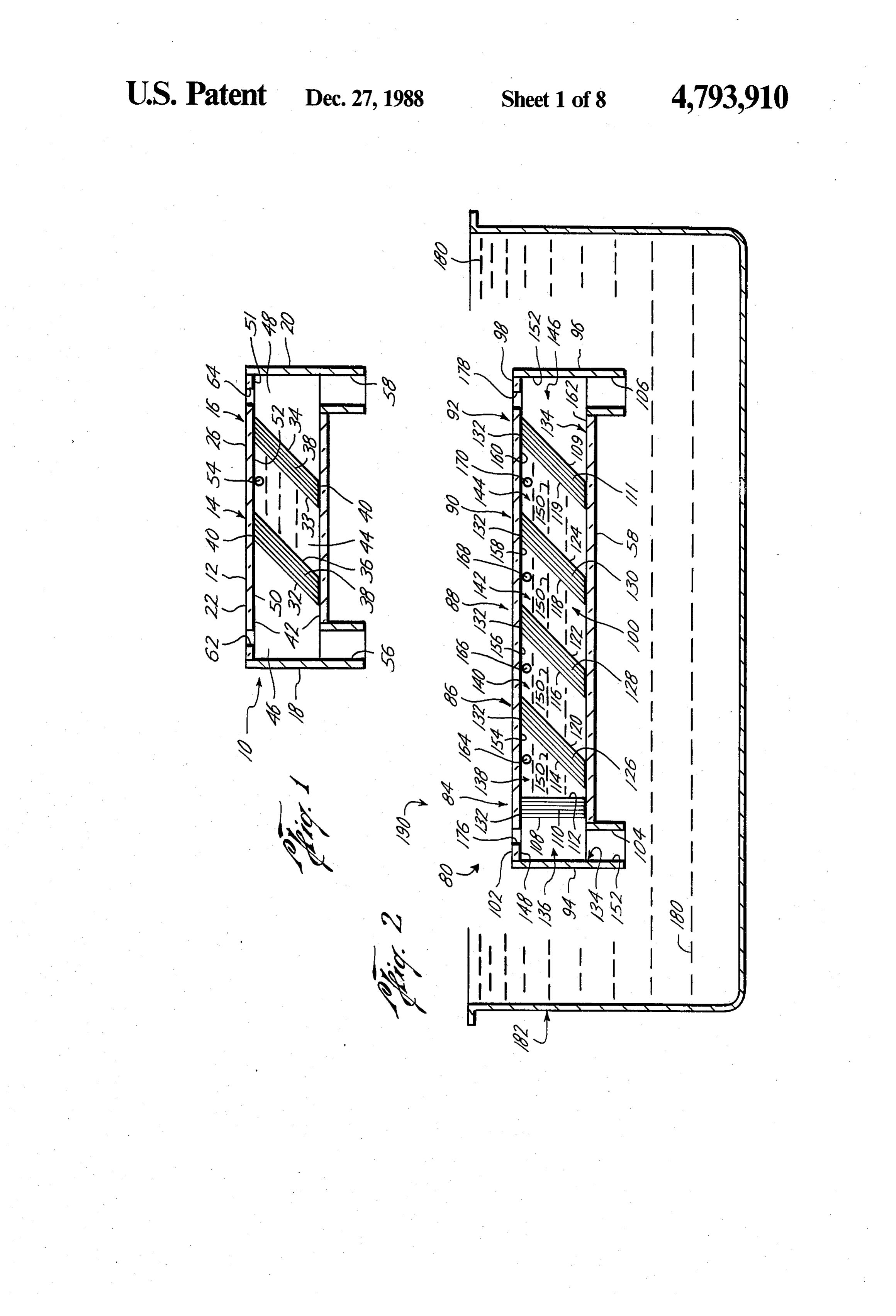
A second exterior bipolar electrode panel is attached cobalt to the housing wall near the second end of the housing. gas-evolvingsulfide, lead sulfide or sulfurized brass and a Said second exterior bipolar electrode panel has a gas compartmentsside are comprising platinum. The internal substantially filled with a first elec evolving side oriented toward the second end and par trolyte such as a fluid polysulfide electrolyte. Such a tially forming a second terminal compartment. The unit may be immersed in an electrolyte second exterior bipolar electrode panel further com a second electrolyte so that a salt bridgebath containing is formed be prises an ohmic contact layer and a semiconductor side. tween the gas-evolving sides of the exterior electrodes The gas-evolving sides of the exterior bipolar electrode 25 panels are preferably catalytic for photodecomposition and then irradiated with a light source such as sunlight. product formation, preferably a metallic catalyst, and Upon such irradiation, oxygen is generated at the gas ideally comprising platinum. The semiconductor sides evolving side of the first exterior bipolar electrode and comprise a p-type or n-type semiconductor, preferably hydrogen at the gas-evolving side of the second exterior a metal chalcogenide such as cadmium selenide or cad 30 bipolar electrode. The gases may be collected. mium sulfide, for example, and said second electrode BRIEF DESCRIPTION OF THE DRAWINGS panel extends across the internal section to physically FIG. 1 shows a vertical cross-sectional view of an separate the internal section on each side of the second electrode panel. embodiment of the multielectrode photoelectrochemi Additionally, the interior photoactive bipolar elec 35 cal unit of the present invention. trode panel-containing multielectrode photoelectro FIG. 2 shows a vertical cross-sectional view of a chemical unit comprises at least one, preferably two, multielectrode photoelectrochemical unit comprising three or more, interior photoactive bipolar electrode several internal compartments, the unit being immersed panels. An interior bipolar electrode panel has a semi in an electrolyte bath.
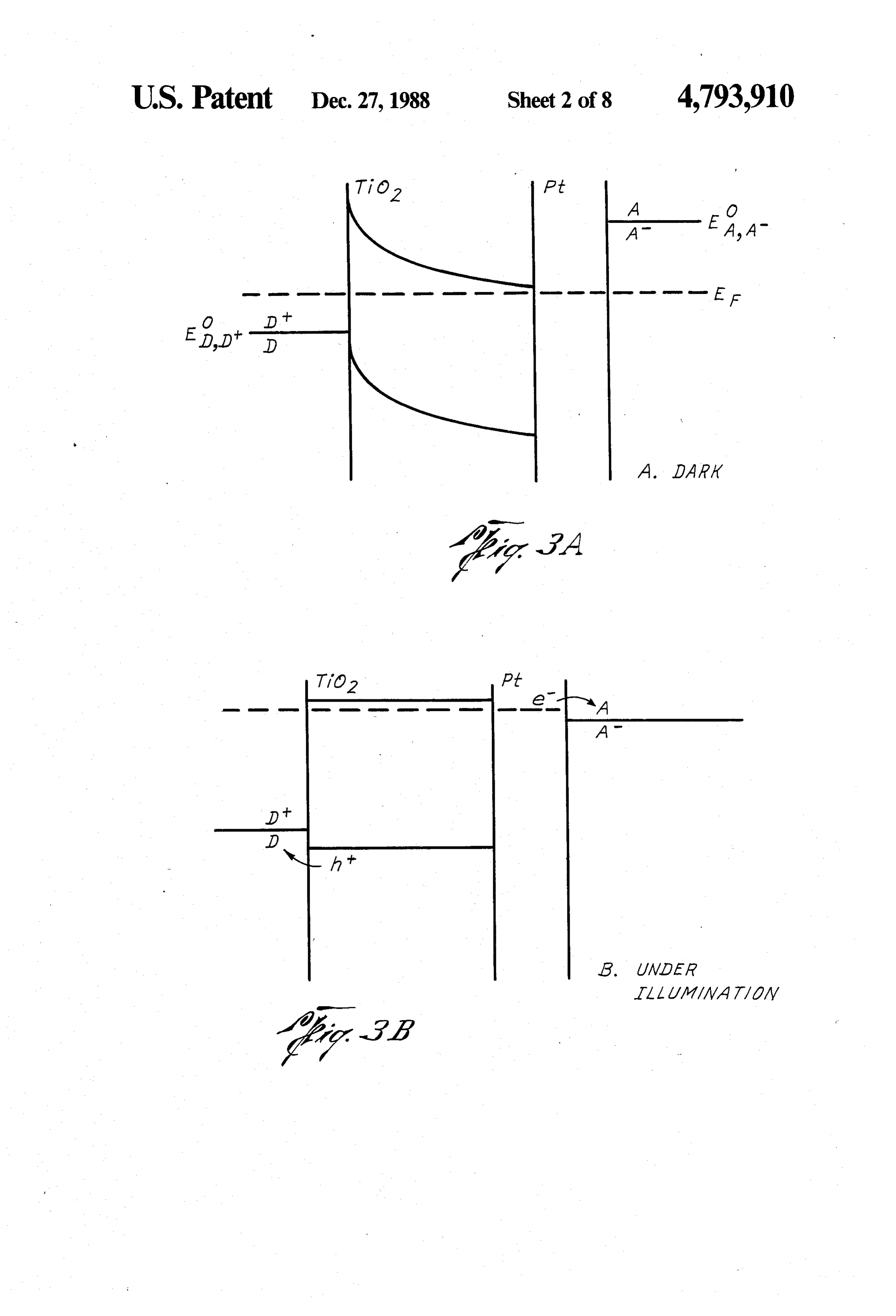
conductor side, an ohmic contact layer and an under FIG.3 shows a schematic representation of TiO2//Pt side. The underside of terminal or interior bipolar elec bipolar electrode in contact with solutions containing trode panels, particularly when the semiconductor is a the D,D and AA couples (A) in the dark at equilib metal chalcogenide, preferably comprises a substance rium and (B) under irradiation.
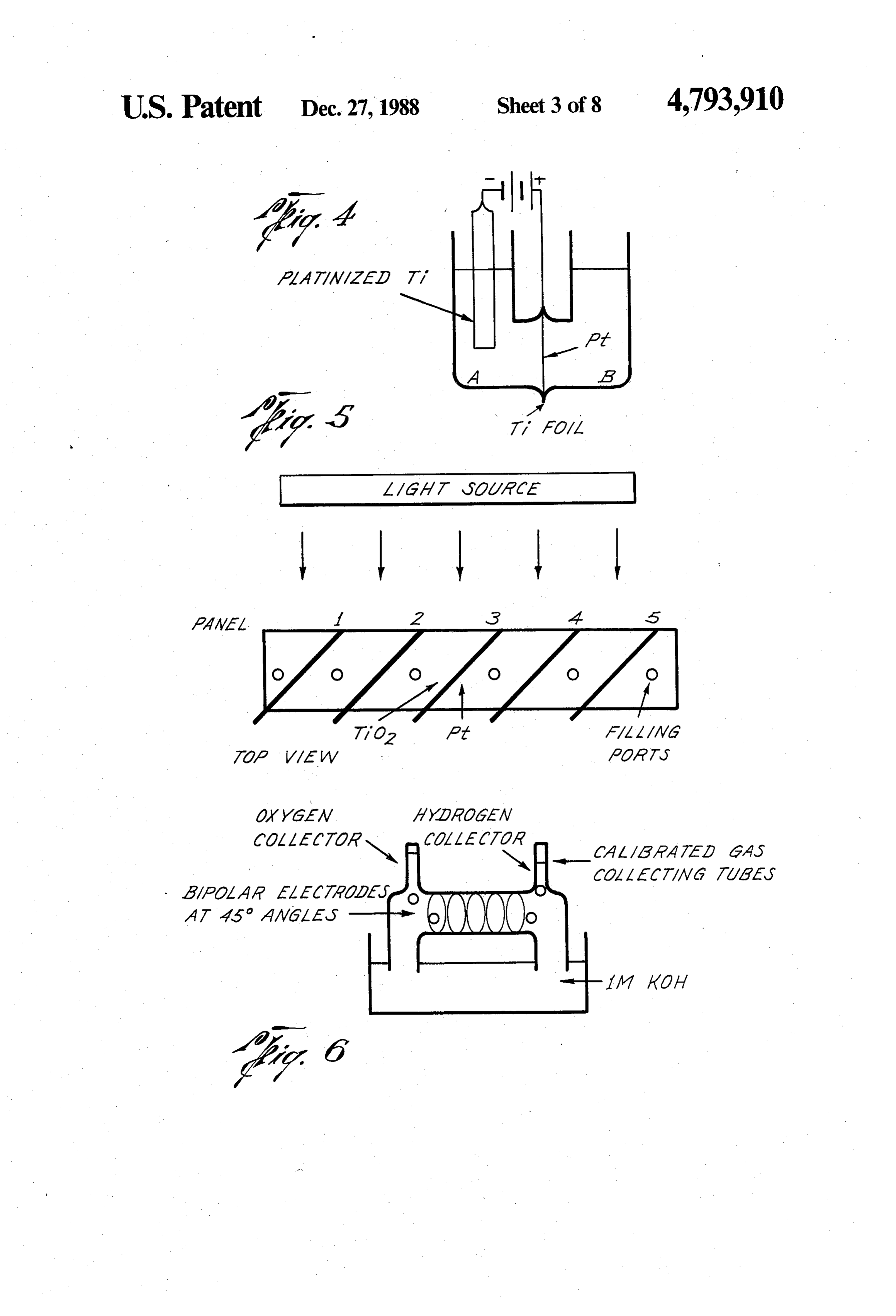
compatible with metal chalcogenides, such as cobalt FIG. 4 shows an anodization cell. Side A contains sulfide, lead sulfide or sulfurized brass, for example. 45 anodizing electrolyte (2.5M H2SO4) in contact with the The interior photoactive bipolar electrode panel is Ti surface to be anodized, with a platinized Ti counter attached to the housing wall in the internal section electrode. Side B contains ice water in contact with the between the exterior bipolar electrode panels. The in platinized Ti surface.
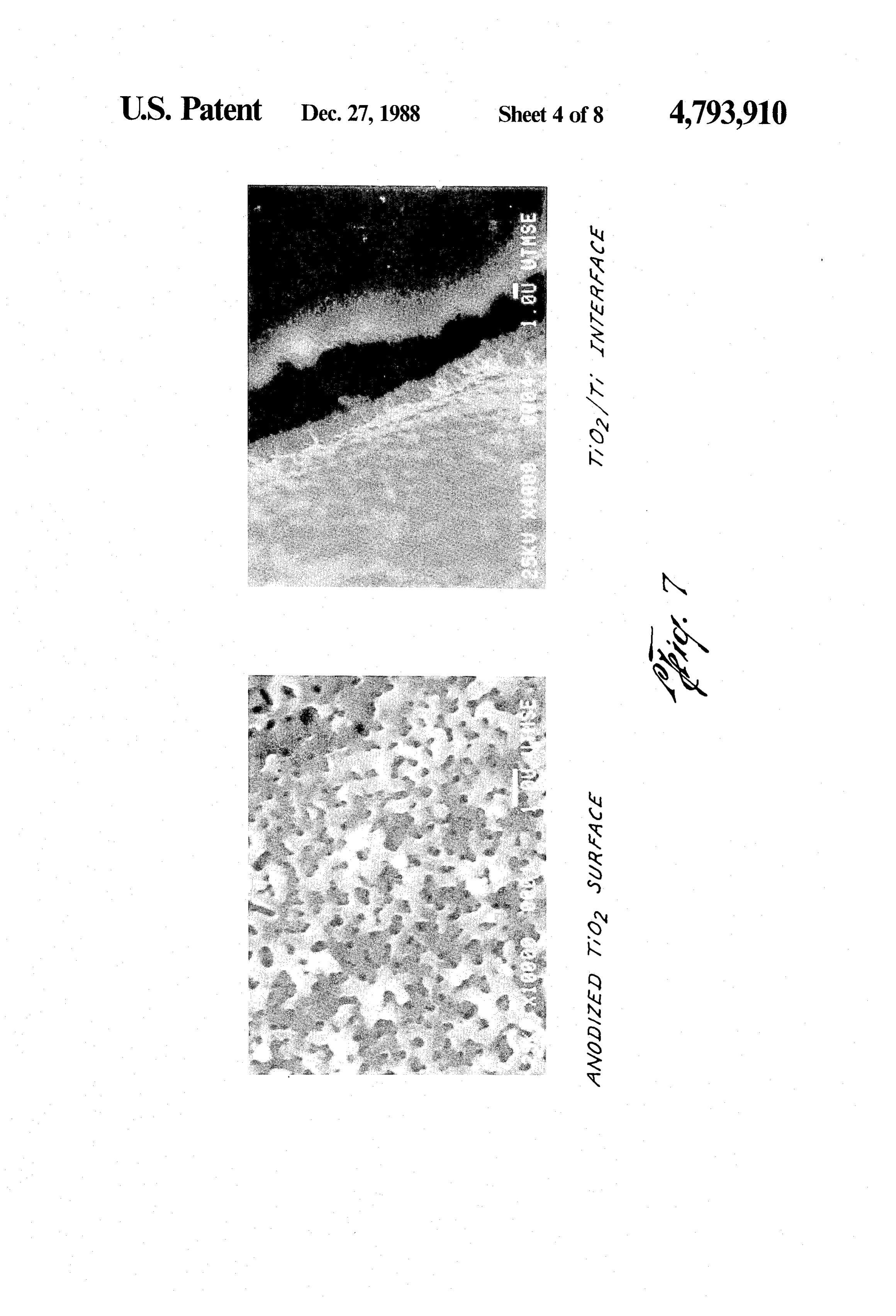
ternal section is divided by interior and exterior bipolar FIG. 5 schematically shows a series array cell. electrode panels into at least two, preferably four, inter 50 FIG. 6 schematically shows a water photoelectrolysis nal compartments. cell with five bipolar electrodes in series. The internal compartments each have a housing wall FIG. 7 shows scanning electron micrographs of an and two ends, each end consisting of a side of an interior odized surface. A. TiO2 treated surface; B. TiO2/Ti or exterior bipolar electrode panel and the housing wall interface.
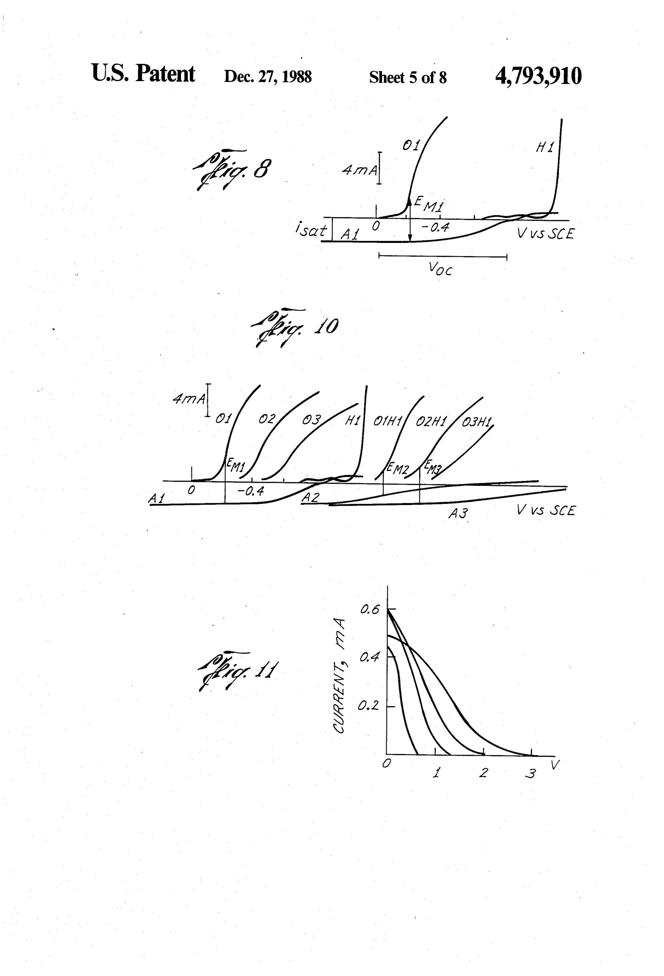
comprising a port for transfer of fluids in or out of the 55 FIG. 8 shows current-potential curves for irradiated internal compartments. The ports are preferably clos TiO2/KOH (A1); Pt/KOH, O2 (01); Pt/KOH (deaer able and may be sealed to isolate internal compartments ated) (H1).
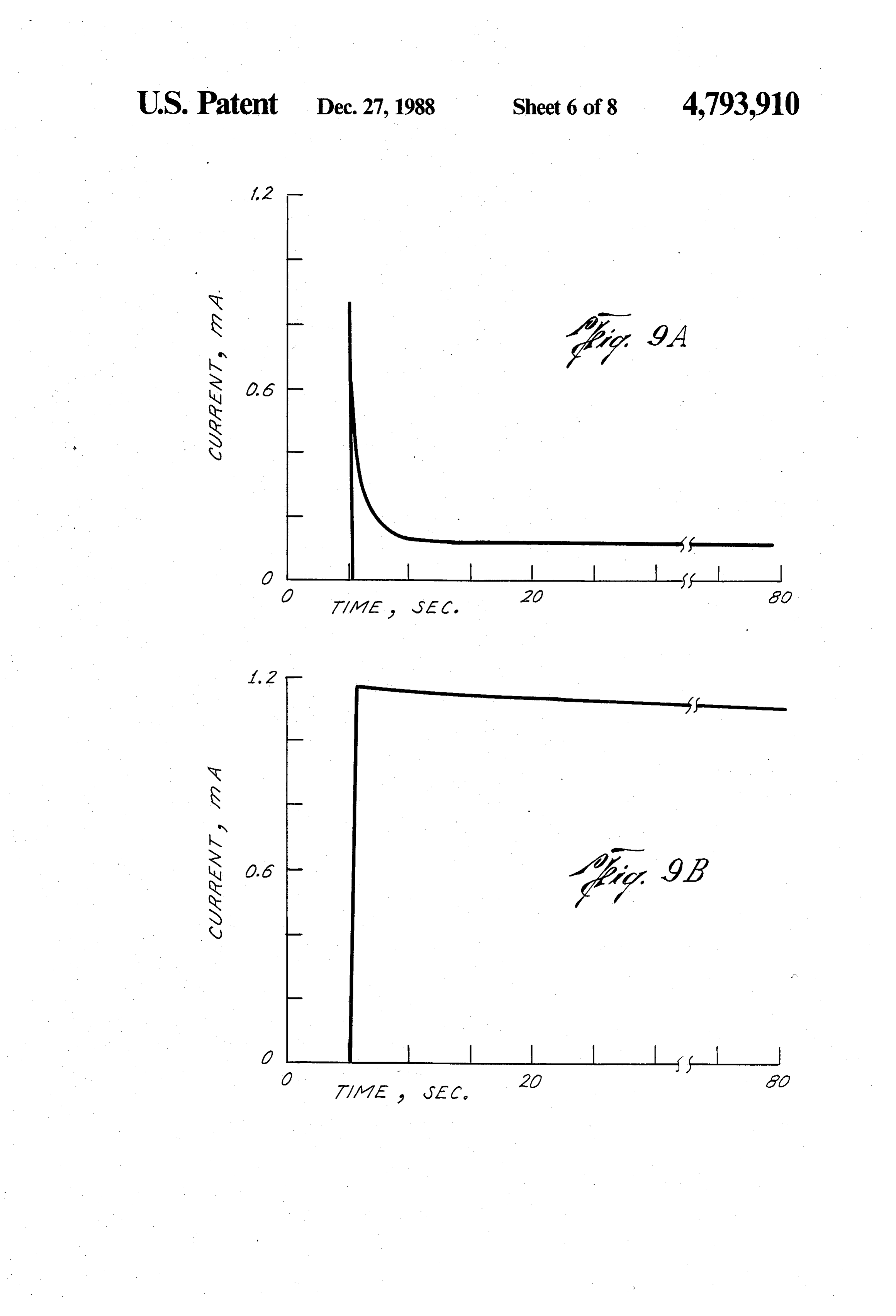
during immersion of the multielectrode photoelectro FIG. 9 shows current vs. time profiles for illuminated chemical unit in an electrolyte bath, for example. TiO2 surface (5.7 cm2) with counterelectrode in 1 M The photoactive bipolar electrode panels, having a 60 KOH. A. Counterelectrode completely immersed. B. semiconductor side, are oriented so that light from an Counterelectrode partially immersed. external source passing into the internal section is sub FIG. 10 shows current-potential characteristics of stantially incident, preferably fully incident, upon a TiO2//Pt panels in 1M KOH.
majority of the semiconductor sides. This orientation 01. Oxygen reduction wave, Pt/KOH, O2. may, for example, be an approximately equal slanting so 65 02. Sum of 201 curves yielding reduction wave for 2 that the photoactive semiconductor sides generally face panels.
toward a light passing side of the housing or may even 03. Sum of 301 curves yielding reduction wave for 3 be parallel to incoming light if effective light-scattering panels. .
Page 12
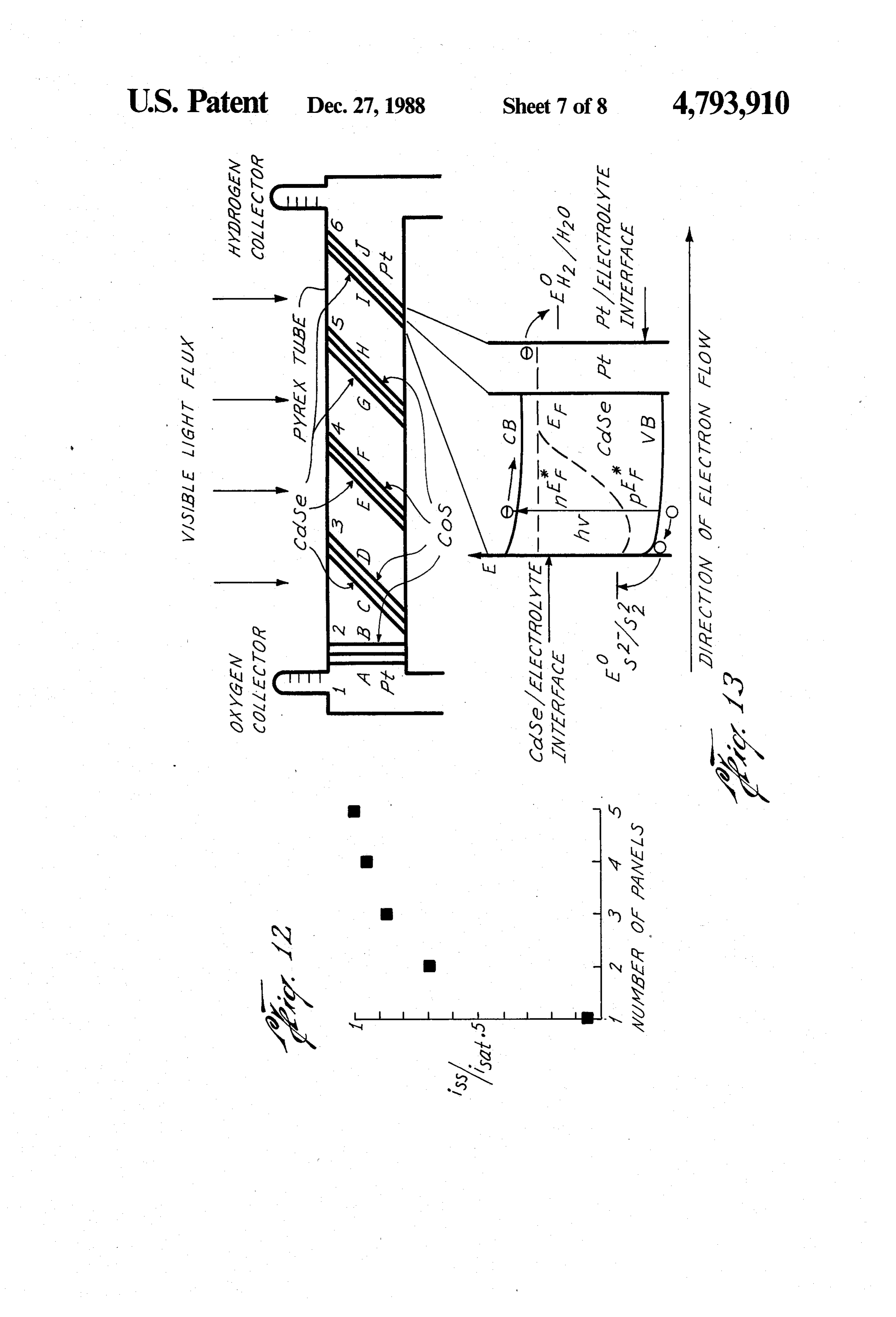
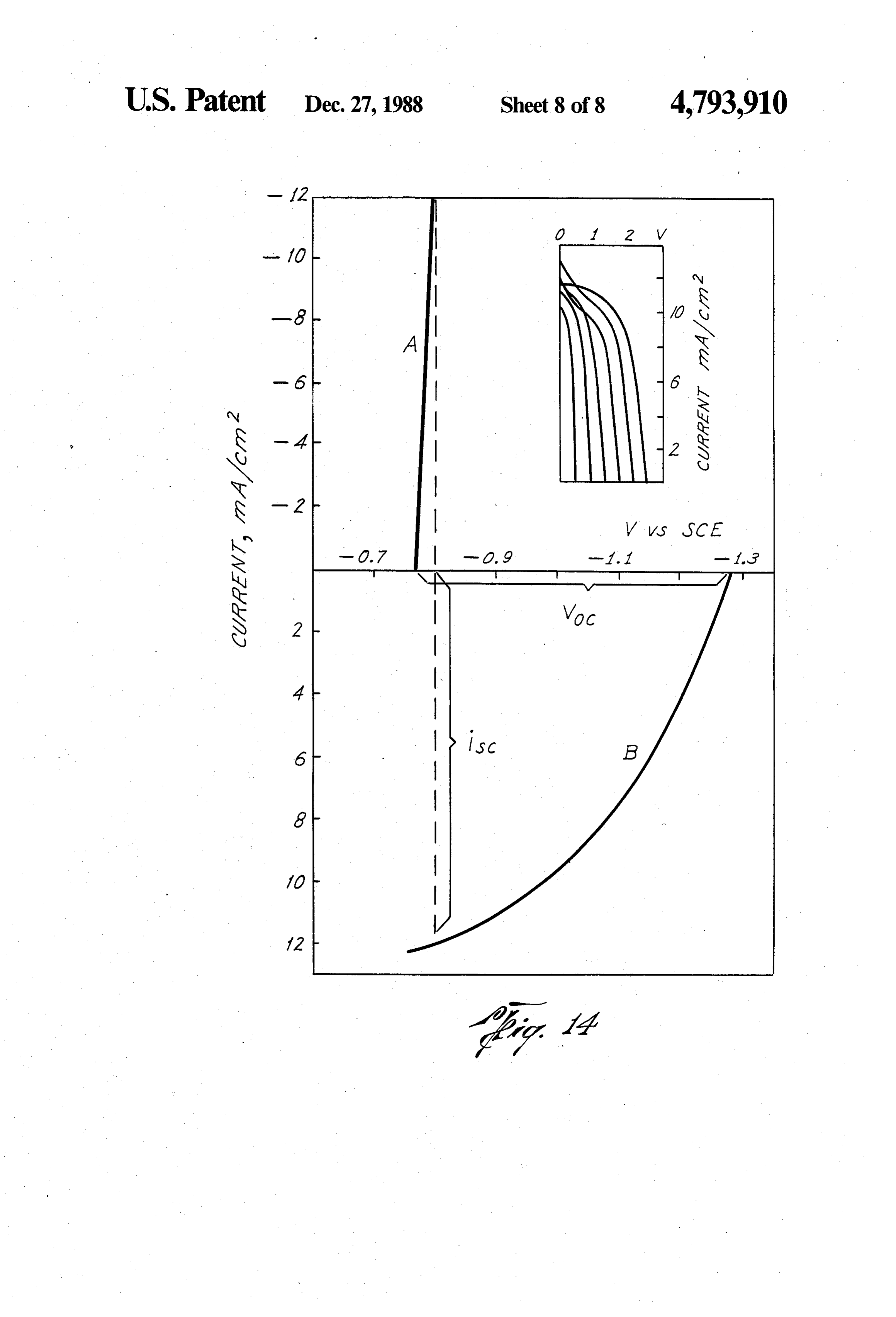
H1. Reduction wave for single panel in outgassed KOH photoelectrochemical unit are at least partially filled solution. with oxygen-saturated first electrolyte. An oxygen-rich OlH1 Reduction wave for H1 biased by 01. gas may be introduced into each interior compartment 02H1 Reduction wave for H1 biased by two 01 panels. to assure oxygen saturation of the first electrolyte. A1 Anodic photocurrent for single panel. 5 To produce a photoelectrochemical cell, the photo A2. Anodic photocurrent for three panels in series, electrochemical unit containing a first electrolyte in one A3 Anodic photocurrent for three panels in series. or more interior compartments is immersed in a bath FIG. 11 shows power curves for TiO2/Pt panels in containing a second electrolyte. The second electrolyte, series. Panel area, 1.0 cm2, in 1M KOH with oxygen upon entering the ports of the terminal compartments, atmosphere. 266 mW/cm2 xenon lamp illumination. 10 forms an electrolytic bridge between externally-facing FIG. 12 shows isc/isat vs. number of panels (1 cm) on sides of the two exterior bipolar electrode panels of the 1M KOH. unit. The externally-facing sides of the exterior bipolar FIG. 13 schematically shows a water photoelectrol electrode panels each define a housing wall of one of the ysis cell. Expansion shows energetics of bipolar panel. two terminal compartments. These terminal compart AJ: PT; B,D,F,H: CoS; C,E,G,I: CdSe, Solutions: 1,6: 15 ments are otherwise defined by the housing and have KOH (1M); 2-5: Na2S (1M), S (1M), KOH (1M). For ports allowing access of an external second electrolyte H2 and O2 generation solutions 1 and 6 are connected and means for collecting evolving gases. When the with KOH bridge. photoelectrochemical cell is irradiated with light ab FIG. 14 shows current-potential characteristics of a sorbable by photoactive bipolar electrode panel semi CdSe//CoS panel in 1:1:1M KOH:S:Na2S solution. 20 conductor sides, O2 is produced at the externally-facing Curve A: polysulfide reduction on dark CoS surface. side of the exterior bipolar electrode panel of one termi Curve B: Oxidation of polysulfide on illuminated CdSe nal compartment and H2 is produced at the externally surface. Effective solar flux: 67.0 mW/cm2. Inset: facing side of the exterior bipolar electrode panel of the power curves for water photoelectrolysis device used in other terminal compartment. The evolving O2 and H2 water photolysis experiment with six photopanels and 25 may be collected by the gas collection means such as one dark CoS panel. Effective solar flux:52.0mW/cm2. storage containers or by any of numerous other means Projected area of each panel: 1.04 cm2. Voc's are in well-known to those skilled in the relevant arts. order from left to right of panels 1 though 6 in series. In accordance with the present invention, a method DESCRIPTION OF THE PREFERRED for unassisted photodecompositions such as the photo 30 lytic splitting of water to form H2 and O2 based on a
EMBODIMENTS multielectrode photoelectrochemical cell is provided. In accordance with the present invention, a multi This method involves use of the above-described photo electrode photoelectrochemical cell useful, for exam electrochemical cell in the manner indicated. ple, for unassisted photolytically induced decomposi An object of the present invention is to provide a tions such as water splitting to form H2 and O2, is pro 35 wireless multielectrode photoelectrochemical cell for vided. This photoelectrochemical cell involves a photo unassisted photolytic water splitting to form H2 and O2 electrochemical unit which comprises a housing with based on an electrolytic bias provided by interior photo housing walls and two ends defining an internal section. active bipolar electrode panels in contact with an O2 For a particularly preferred embodiment, contained in saturated electrolyte solution.
the housing are at least two photoactive bipolar elec One advantage of the photoelectrochemical cell of trode panels mounted across the internal section to form the present invention is that an expenditure of energy in a multielectrode series array. addition to incident radiant (e.g., solar) energy is not Each photoactive bipolar electrode panel has a semi required for photolytic water splitting. The photoelec conductor side and a catalytic side or underside. The trochemical cell of the present invention is simple in photoactive bipolar electrode panels are situated in the 45 construction, involves no electrical wiring between housing and aligned so that their semiconductor sides bipolar electrode panels, and allows a ready collection face the same general direction. The bipolar electrode of product gases such as H2 and O2 for various uses. panels divide the volume enclosed by the housing into Other photoelectrochemical devices having the same compartments. Internal compartments are located in general purpose fail to demonstrate these advantageous the internal housing section between the two exterior 50 properties.
bipolar electrode panels and terminal compartments DESCRIPTION OF THE PREFERRED border the internal faces of each exterior bipolar elec EMBODIMENTS trode panel.
The housing is at least partially constructed of mate The invention will be described in terms of preferred rial which allows irradiation of the semiconductor sides 55 embodiments which represent the best mode known to of the photoactive bipolar electrode panels mounted the applicants at the time of this application. therein by a source of light external to the housing. The FIG. 1 shows a multielectrode photoelectrochemical interior compartments have a port and are capable of unit 10 according to a preferred embodiment of the retaining a first electrolyte. The first electrolyte is pref. present invention. In accordance with such preferred erably oxygen-saturated. An oxygen-rich gas may also 60 embodiment, multielectrode photoelectrochemical unit be retained within the interior compartments to assure 10 comprises a housing 12 a first bipolar electrode panel maintenance of an O2-saturated first electrolyte. Each 14 and a second bipolar electrode panel 16. It is contem of the two terminal compartments comprises a port for plated that two bipolar electrode panels is the minimum liquid access and may have a means for gas collection. workable number for the purposes of the present inven Each interior compartment has a closable port which is 65 tion.
an orifice in the housing wall. The port may be used to The housing 12 comprises a first end 18, a second end add liquid orgas to the compartment. For photoelectro 20 and a housing wall 22. The housing wall 22 and ends chemical operation, the interior compartments of the 18, 20 define the internal section 24 of the housing 12. A
Page 13
particularly preferred housing usable in connection bipolar electrode panels 14, 16 partially defining the with the present invention is a length of corrosion internal compartment 44 are substantially covered by resistant tubing which comprises a transparent material the electrolyte. A quantity of oxygen-rich gas may also such as temperature-resistant glass. The housing 12 has be introduced through the filling port 54 into the inter at least one light-passing or transparent side 26. nal compartment 44. The internal compartment 44 may Each bipolar electrode panel 14, 16 comprises a semi then be closed by sealing the filling port 54. conductor side 32, 33 a catalytic side 34 or an underside The terminal compartments 46, 48 each have a liquid 36 and an ohmic contact layer 38. The bipolar electrode access port 56, 58. At least one terminal compartment panels 14, 16 are mounted within the housing 12 and are 46, 48 also has a means for collecting gaseous photode attached at their edges 40 to the inside surface 42 of the O composition products. This means for collecting may housing wall 22 to partially define an internal compart comprise a gasport 62, 64. The liquid access ports 56, 58 ment 44, a first terminal compartment 46 and a second and the gas ports 62, 64 are orifices in portions 50, 51 of terminal compartment 48. The semiconductor side 32 of the housing wall 22, which, along with the first bipolar the first bipolar electrode panel 14 and a portion 50 of electrode panel 14 and second bipolar electrode panel the internal surface 42 of the housing wall 22 define the 16, partially
define the first terminal compartment 46 first terminal compartment 46 at the first end 18 of the and the second terminal compartment 48 respectively. housing 12. A second terminal compartment 48 at the second end 20 of the housing 12 is defined by the cata to an embodimentwater
To describe a photolysis operation according of the present invention, an electro lytic side 34 of the second bipolar electrode panel 16 lyte is added through the filling port 54 of the internal and a portion 51 of the inside surface 42 of the housing 20 compartment 44 to a suitable level substantially cover wall 22. An internal compartment 44 is defined by the ing the sides 33, underside 36 of the first bipolar electrode panel 14, the one embodiment, 36 of the bipolar electrodes 14,16. In an oxygen-rich gas is added above the semiconductor side 33 of the second bipolar electrode electrolyte so that panel 16 and a portion 52 of the inside surface 42 of the formed in the internalancompartment O2-saturated is maintained or 44 of the multielec housing wall 22. 25
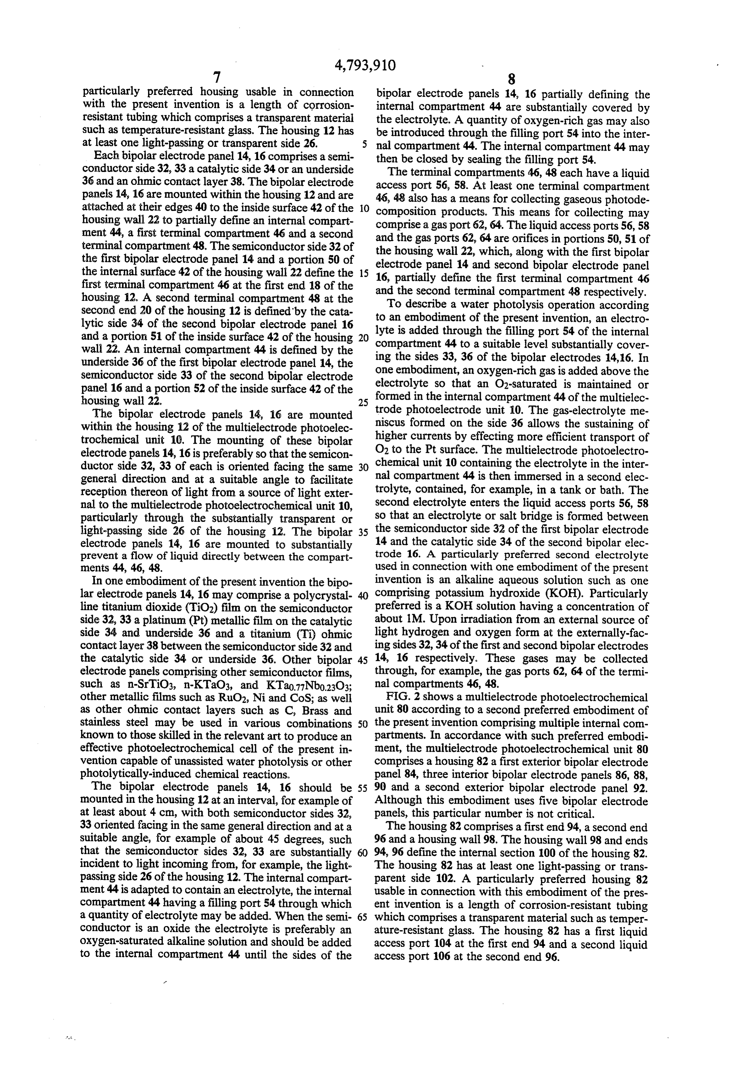
The bipolar electrode panels 14, 16 are mounted trode photoelectrode unit 10. The gas-electrolyte me within the housing 12 of the multielectrode photoelec miscus formed on the side 36 allows the sustaining of trochemical unit 10. The mounting of these bipolar higher currents by effecting more efficient transport of electrode panels 14, 16 is preferably so that the semicon O2 to the Pt surface. The multielectrode photoelectro ductor side 32, 33 of each is oriented facing the same 30 chemical unit 10 containing the electrolyte in the inter general direction and at a suitable angle to facilitate nal compartment 44 is then immersed in a second elec reception thereon of light from a source of light exter trolyte, contained, for example, in a tank or bath. The nal to the multielectrode photoelectrochemical unit 10, second electrolyte enters the liquid access ports 56, 58 particularly through the substantially transparent or so that an electrolyte or salt bridge is formed between light-passing side 26 of the housing 12. The bipolar 35 the semiconductor side 32 of the first bipolar electrode electrode panels 14, 16 are mounted to substantially 14 and the catalytic side 34 of the second bipolar elec prevent a flow of liquid directly between the compart trode 16. A particularly preferred second electrolyte ments 44, 46, 48. used in connection with one embodiment of the present In one embodiment of the present invention the bipo invention is an alkaline aqueous solution such as one lar electrode panels 14, 16 may comprise a polycrystal comprising potassium hydroxide (KOH). Particularly line titanium dioxide (TiO2) film on the semiconductor preferred is a KOH solution having a concentration of side 32, 33 a platinum (Pt) metallic film on the catalytic about 1.M. Upon irradiation from an external source of side 34 and underside 36 and a titanium (Ti) ohmic light hydrogen and oxygen form at the externally-fac contact layer 38 between the semiconductor side 32 and ing sides 32, 34 of the first and second bipolar electrodes the catalytic side 34 or underside 36. Other bipolar 45 14, 16 respectively. These gases may be collected electrode panels comprising other semiconductor films, through, for example, the gas ports 62, 64 of the termi such as n-SrTiO3, n-KTaO3, and KTao.77NbO23O3; nal compartments 46, 48.
other metallic films such as RuO2, Ni and CoS; as well FIG. 2 shows a multielectrode photoelectrochemical as other ohmic contact layers such as C, Brass and unit 80 according to a second preferred embodiment of stainless steel may be used in various combinations 50 the present invention comprising multiple internal com known to those skilled in the relevant art to produce an partments. In accordance with such preferred embodi effective photoelectrochemical cell of the present in ment, the multielectrode photoelectrochemical unit 80 vention capable of unassisted water photolysis or other comprises a housing 82 a first exterior bipolar electrode photolytically-induced chemical reactions. panel 84, three interior bipolar electrode panels 86, 88, The bipolar electrode panels 14, 16 should be 55 90 and a second exterior bipolar electrode panel 92. mounted in the housing 12 at an interval, for example of Although this embodiment uses five bipolar electrode at least about 4 cm, with both semiconductor sides 32, panels, this particular number is not critical. 33 oriented facing in the same general direction and at a The housing 82 comprises a first end 94, a second end suitable angle, for example of about 45 degrees, such 96 and a housing wall 98. The housing wall 98 and ends that the semiconductor sides 32, 33 are substantially 94, 96 define the internal section 100 of the housing 82. incident to light incoming from, for example, the light The housing 82 has at least one light-passing or trans passing side 26 of the housing 12. The internal compart parent side 102. A particularly preferred housing 82 ment 44 is adapted to contain an electrolyte, the internal usable in connection with this embodiment of the pres compartment 44 having a filling port 54 through which ent invention is a length of corrosion-resistant tubing a quantity of electrolyte may be added. When the semi 65 which comprises a transparent material such as temper conductor is an oxide the electrolyte is preferably an ature-resistant glass. The housing 82 has a first liquid oxygen-saturated alkaline solution and should be added access port 104 at the first end 94 and a second liquid to the internal compartment 44 until the sides of the access port 106 at the second end 96.
Page 14
The first exterior bipolar electrode panel 84 prefera 109 of bipolar electrode panels of the present invention bly comprises a catalytic side 108, an ohmic contact may comprise films of materials such as RuO2, degener layer 110 and an underside 112. Each interior bipolar atively doped Cdx (X=S,Se, Te) or CoS; or metallic electrode panel 86, 88,90 comprises a semiconductor films such as Ni, Pt and platinized Ti. Ohmic contact side 114, 116, 118, an underside 120, 122, 124 and an 5 layers 110, 126, 128, 130, 111, in addition to the titanium ohmic contact layer 126, 128,130. The bipolar electrode foil described herein may be of materials such as C, panels 84, 86, 88,90, 92 are mounted within the housing Brass and stainless steel which may be used in various 82 and are attached at their edges 122 to the inner sur combinations known to those skilled in the relevant art. face 134 of the housing 82 wall 98 to partially define six The undersides 112, 120, 122, 124 of bipolar electrode compartments 136, 138,140,142,144, 146. The catalytic 10 panels 84, 86, 88, 90 should be chemically compatible side 108 of the first exterior bipolar electrode panel 84 with the semiconductor sides 114, 116, 118, 119 being and a portion 148 of the inner surface 134 of the housing used (such as the cobalt sulfide undersides and the cad wall 98 partially define the first terminal compartment mium sulfide semiconductor sides of the example pres 136 at the first end 94 of the housing 82. A second termi ented herein) to produce an effective photoelectro nal compartment 146 at the second end 96 of the hous 15 chemical cell of the present invention capable of unas ing 82 is partially defined by the catalytic side 109 of the sisted water photolysis.
second exterior bipolar electrode panel 92 and a portion The photosensitive bipolar electrode panels 86, 88, 152 of the inner surface 134 of the housing 82 wall 98. 90, 92 may be mounted in the housing 82 at intervals, for A first internal compartment 138 is partially defined example of about 4 cm, with all semiconductor sides by the underside 112 of the first exterior bipolar elec 20 114, 116, 118, 119 oriented in the same general direction trode panel 84, the semiconductor side 114 of the first and at a suitable angle, for example of about 45 degrees, interior bipolar electrode panel 86 and a portion 154 of such that the semiconductor sides 114, 116, 118, 119 are the inner surface 134 of the housing 82 wall 98. The substantially incident to light from an external source second internal compartment 140 is partially defined by directed into the internal section 100 through a light the underside 120 of the first interior bipolar electrode 25 passing side 102 of the housing 82. The bipolar elec panel 86, the semiconductor side 116 of the second trode panels 84, 86, 88,90, 92 separate the internal sec interior bipolar electrode panel 88 and a portion 156 of tion 100 of the housing 82 into compartments 136, 138, the inner surface 134 of the housing 82 wall 98. The 140, 142,444, 146 as described above. The internal com third internal compartment 142 is partially defined by partments 138, 140, 142, 144 are adapted to contain a the underside 122 of the second interior bipolar elec-30 first electrolyte 150 which may be O2-saturated or con trode panel 88, the semiconductor side 118 of the third tain a polysulfide, depending upon the desired compati interior bipolar electrode panel 90 and a portion 158 of bility with the semiconductor system being used. the inner surface 134 of the housing 82 wall 98. The Each internal compartment 138, 140, 142, 144, has a fourth internal compartment 144 is partially defined by filling port 164, 166, 168, 170 through which a quantity the underside 124 of the third interior bipolar electrode 35 of first electrolyte 150 may be introduced, supple panel 90, the semiconductor side 119 of the second mented or extracted. Each filling port 164, 166, 168, 170 exterior bipolar electrode panel 92 and a portion 160 of is characterized as being a closable orifice opening the inner surface 134 of the housing 82 wall 98. The through a portion 154, 156,158, 160 of the inner surface second terminal compartment 146 is partially defined by 134 of the housing 82.
the catalytic side 109 of the second exterior bipolar 40 A first electrolyte 150 compatible with the semicon electrode panel 92 and a portion 162 of the inner surface ductor being utilized is added to the internal compart 134 of the housing 82 wall 98. ments 138, 140, 142, 144 until the sides of the bipolar The bipolar electrode panels 84, 86, 8890, 92 are electrode panels 84, 86, 88,90, 92 partially defining the mounted within the housing 82 of the multielectrode internal compartments are at least substantially covered photoelectrochemical unit 80. The mounting of these 45 by the first electrolyte 150. A quantity of oxygen-rich bipolar electrode panels 84, 86, 88,90, 92 is preferably gas may, if desired, also be introduced through the so that each semiconductor side 114, 116, 118, 119 is upper filling ports 164, 166, 168, 170 into the internal oriented facing in the same general direction and at a compartments. The internal compartments 138, 140, suitable angle to facilitate reception thereon of light 142, 144 are then closed by sealing the filling ports 164, from a source of light external to the multielectrode 50 166, 168, 170, for example, with rubber stoppers (not photoelectrochemical unit 80. Light from the external shown).
source (not shown) penetrates the housing 82, prefera The terminal compartments 136, 146 each have a bly through a light-passing or transparent side 102. The liquid access port 104,106 through an adjacent portion bipolar electrode panels 84, 86, 88,90, 92 are mounted 152, 162 of the inner surface 134 of the housing 82 and to substantially prevent a direct flow of liquid between 55 at least one also has a means for collecting gaseous the compartments 136, 138, 140, 142, 144, 146. photodecomposition products. Such means generally Preferably used in connection with this embodiment involve a gas port 176, 178 through an adjacent portion of the present invention were semiconductor-contain 152, 162 of the inner surface 134 of the housing 82 as ing bipolar electrode panels 86, 88,90, 92 comprising a shown in FIG. 2. The gas ports 176, 178 may be used for cadmium selenide (CdSe) film on semiconductor sides an active or passive transport and collection of gener 114, 116, 118, 119. A platinum (Pt) film comprised the ated gases.
catalytic side 108, 109 of exterior bipolar electrodes 84, To describe a water photolysis operation according 92. A titanium (Ti) ohmic contact layer 110, 126, 128, to the present invention, a first electrolyte 150 is added 130, 111 comprised the innermost layer of all the bipolar through a filling port 164, 166, 168, 170 of each internal electrode panels 84, 86, 88,90, 92. Photosensitive bipo 65 compartment 138, 140, 142, 144 to a suitable level and, lar electrode panels usable in the practice of the present depending upon the semiconductors being used, a poly invention may comprise semiconductor films, such as sulfide supplement or an oxygen-rich gas may be added CdTe, CaAs, and CdSe Te. The catalytic sides 108, above the first electrolyte 150, in the latter case so that

Page 15
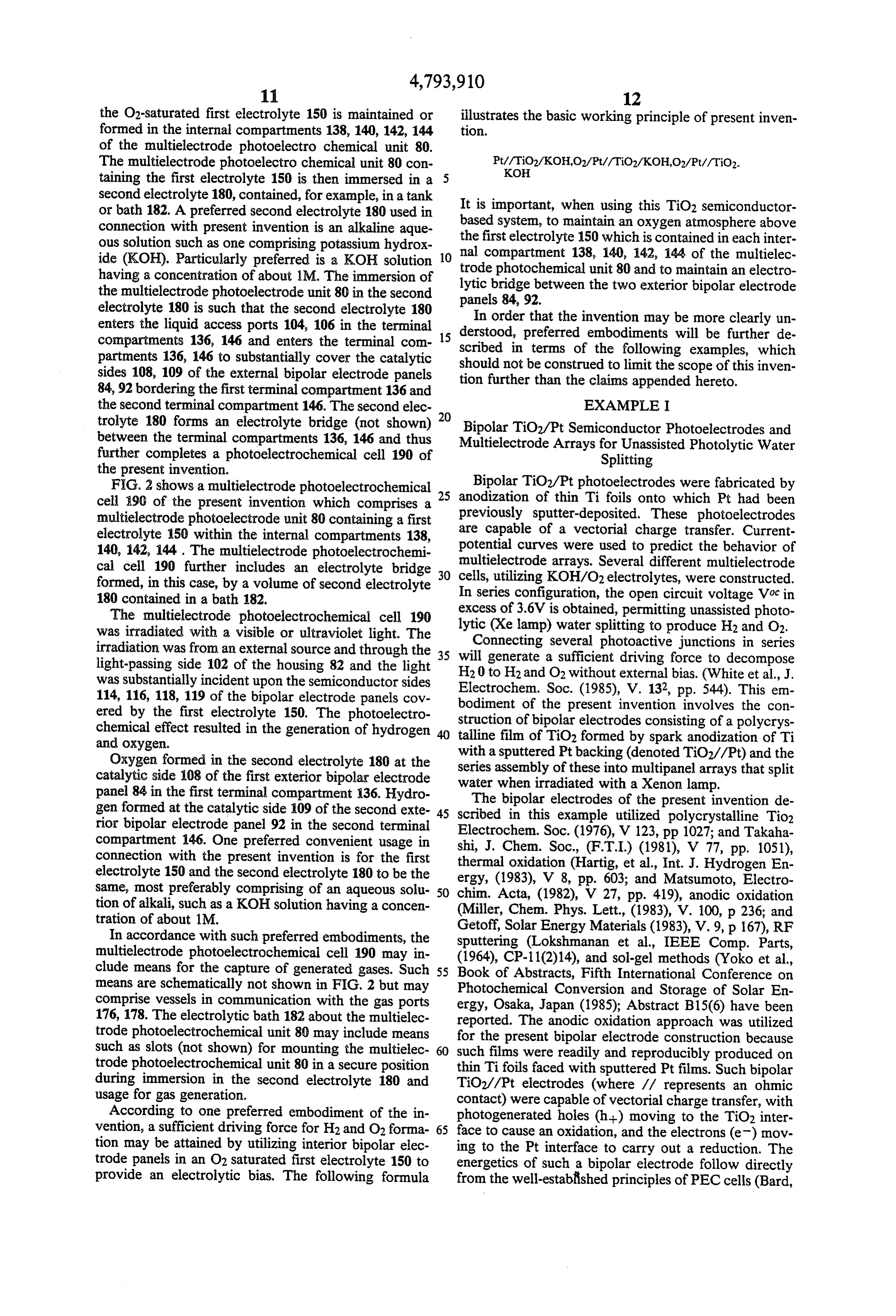
the O2-saturated first electrolyte 150 is maintained or illustrates the basic working principle of present inven formed in the internal compartments 138, 140, 142,144 tion.
of the multielectrode photoelectro chemical unit 80.
The multielectrode photoelectro chemical unit 80 con taining the first electrolyte 150 is then immersed in a second electrolyte 180, contained, for example, in a tank or bath 182. A preferred second electrolyte 180 used in It is important, when using this TiO2 semiconductor connection with present invention is an alkaline aque based system, to maintain an oxygen atmosphere above ous solution such as one comprising potassium hydrox the first electrolyte 150 which is contained in each inter mal compartment 138, 140, 142, 144 of the multielec ide (KOH). Particularly preferred is a KOH solution 10 trode having a concentration of about lM. The immersion of lytic bridgephotochemical unit 80 and to maintain an electro the multielectrode photoelectrode unit 80 in the second panels 84, 92.between the two exterior bipolar electrode electrolyte 180 is such that the second electrolyte 180 In order that the invention may be more clearly un enters the liquid access ports 104, 106 in the terminal 5 derstood, compartments 136, 146 and enters the terminal com- 1 scribed inpreferred embodiments will be further de partments 136, 146 to substantially cover the catalytic should not be construedtheto following terms of limit the examples, which scope of this inven sides 108, 109 of the external bipolar electrode panels tion further than the claims appended hereto. 84, 92 bordering the first terminal compartment 136 and the second terminal compartment 146. The second elec 20 EXAMPLE I trolyte 180 forms an electrolyte bridge (not shown) Bipolar TiO2/Pt Semiconductor Photoelectrodes and between the terminal compartments 136, 146 and thus Multielectrode Arrays for Unassisted Photolytic Water further completes a photoelectrochemical cell 190 of Splitting the present invention.
Bipolar TiO2/Pt photoelectrodes
FIG. 2 shows a multielectrode photoelectrochemical 25 anodization of thin Ti foils onto which were fabricated by cell 90 of the present invention which comprises a previously sputter-deposited. These photoelectrodes Pt had been multielectrode photoelectrode unit 80 containing a first electrolyte 150 within the internal compartments 138, are capable of a vectorial charge transfer. Current 140, 142, 144. The multielectrode photoelectrochemi potential curves were used to predict the behavior of multielectrode arrays. Several different multielectrode cal ceil 190 further includes an electrolyte bridge 30 cells, utilizing KOHMO2 electrolytes, were constructed. formed, in this case, by a volume of second electrolyte In series configuration, the open circuit voltage Voc in 180 contained in a bath 182.
The multielectrode photoelectrochemical cell 190 lytic excess of 3.6V is obtained, permitting unassisted photo was irradiated with a visible or ultraviolet light. The (Xe lamp) water splitting to produce H2 and O2. Connecting several photoactive junctions in series irradiation was from an external source and through the 5 will generate a sufficient driving force to decompose light-passing side 102 of the housing 82 and the light H20 to H2 and O2 without external bias. (White et al., J. was substantially incident upon the semiconductor sides Electrochem. Soc. (1985), V. 132, pp. 544). This en 114, 116, 118, 119 of the bipolar electrode panels cov ered by the first electrolyte 150. The photoelectro bodiment struction of of the present invention involves the con bipolar electrodes consisting of a polycrys chemical effect resulted in the generation of hydrogen talline film of TiO2 formed by spark anodization of Ti and oxygen.
Oxygen formed in the second electrolyte 180 at the series assembly ofPtbacking with a sputtered (denoted TiO2//Pt) and the these into multipanel arrays that split catalytic side 108 of the first exterior bipolar electrode water when irradiated with a Xenon lamp. panel 84 in the first terminal compartment 136. Hydro gen formed at the catalytic side 109 of the second exte 45 scribed bipolar
The in this electrodes of the present invention de example utilized polycrystalline Tio2 rior bipolar electrode panel 92 in the second terminal Electrochem. Soc.
compartment 146. One preferred convenient usage in shi, J. Chem. Soc.,(1976), V 123, pp 1027; and Takaha
connection with the present invention is for the first thermal oxidation (Hartig, et al., Int. J. Hydrogen En electrolyte 150 and the second electrolyte 180 to be the same, most preferably comprising of an aqueous solu 50 ergy, (1983), V 8, pp. 603; and Matsumoto, Electro tion of alkali, such as a KOH solution having a concen (Miller,Acta,
tration of about 1M.
In accordance with such preferred embodiments, the Getoff, Solar Energy Materials (1983), V. 9, p 167), RF multielectrode photoelectrochemical cell 190 may in sputtering (Lokshmanan et al., IEEE Comp. Parts, clude means for the capture of generated gases. Such 5 5 (1964), CP-11(2)14), and sol-gel methods (Yoko et al., Book of Abstracts, Fifth International Conference on means are schematically not shown in FIG. 2 but may Photochemical Conversion and Storage of Solar En comprise vessels in communication with the gas ports ergy, Osaka, Japan (1985); Abstract B15(6) have been 176, 178. The electrolytic bath 182 about the multielec reported. The anodic oxidation approach was utilized trode photoelectrochemical unit 80 may include means for the present bipolar electrode construction because such as slots (not shown) for mounting the multielec 60 such films were readily and reproducibly produced on trode photoelectrochemical unit 80 in a secure position thin Tifoils faced with sputtered Pt films. Such bipolar during immersion in the second electrolyte 180 and TiO2//Pt electrodes (where // represents an ohmic usage for gas generation. contact) were capable of vectorial charge transfer, with According to one preferred embodiment of the in photogenerated holes (h) moving to the TiO2 inter vention, a sufficient driving force for H2 and O2 forma 65 face to cause an oxidation, and the electrons (e) mov tion may be attained by utilizing interior bipolar elec ing to the Pt interface to carry out a reduction. The trode panels in an O2 saturated first electrolyte 150 to energetics of such a bipolar electrode follow directly provide an electrolytic bias. The following formula from the well-established principles of PEC cells (Bard,
Page 16
Science, (1980), V. 207, p. 139) as shown schematically trolyte in the interior cells. The gas collecting tubes on in FIG. 3. The analysis of the electrochemical behavior the end cells were calibrated to permit monitoring of of a single bipolar electrode for actual redox couples gas volume with time. The evolution of hydrogen and and of series connected multijunction cells can be car oxygen was confirmed by gas chromatographic analysis ried out by graphical addition of current-potential (i-V using a column packed with 50 g of 13X, 60/80 mesh, curves (White et al., cited above), as described below. sieves from Alltech Associates Inc., with argon as the Photosensitive TiO2 films were prepared by the high carrier gas at 30 mL/min.
voltage anodization technique reported by Marchenoir Photoelectrochemical Behavior of single TiO2//Pt et al., (Thin Solid Films (1980), V. 66, p.357) and Miller
(Chem. Phys. Lett. (1983), V. 100, p. 236). The Ti foil, 10 Panels.
about 2
The TiO2 films formed by anodization were um thick with pore diameters of about 1000 A.
purchased from Johnson Matthey, Inc., had a thickness X-ray diffraction measurements showed powder pat of 0.025 mm and a purity of 99.7%. The Ti foil was terns characteristic of both rutile and anatase phases as degreased in methylene chloride and rinsed in distilled well as Ti2O3, TiO, add Timetal, suggesting a gradient water. One side of the foil was coated with a Pt film ca. of oxides with the lower oxides nearer the Ti surface. 350 nm thick by RF sputtering with a Materials Re 15 One form of bipolar electrode consisted of a free-stand search Co., (Orangeburg, NY) model 8620 sputtering ing TiO2 file produced by spark anodizing the Ti foil to apparatus at 2x10² torr Ar with a deposition rate of form a TiO2 film, RF sputtering of Pt onto the TiO2, 10A/s. The platinized foil was cut into 3x3 cm squares and dissolving and the Tiside was subjected to spark anodization in the containing 20%theBr2.remaining The Ti substrate in methanol resulting TiO2/Pt film was cell shown in FIG. 4. Sulfuric acid (2.5M) was used as 20 the electrolyte facing the Ti side with a platinized tita handled with Nylon mesh. However, it was easier to platinize the Tibefore anodization of the opposite side, nium foil serving as the cathode. Side B, facing the Pt, and this configuration was used in all of the experiments was filled with ice water to cool the electrode during of this Example described below. the anodization. The Tifoil, which served as the anode, The photoelectrochemical behavior of the bipolar was glued between the cells with silicone cement. The 25 panel was voltage between the Tilfoils was gradually increased of each sideelucidated by studying the i-V characteristics independently. For this purpose the panel with the current density never exceeding 35 mA/cm2. was clamped between two solutions in the configura Sparking began at 95V and continued up to the final tion of FIG. 2. The resulting i-V curves applied voltage, 125V; at this point the electrolyte was faces TiO2/KOH (A1); Pt/KOH, O2for(01); the inter replaced and the final voltage maintained for 10 min. 30 Pt/KOH (H1, deaerated with Ar) are shown in FIG.and8 The anodized foil, with a TiO2 film thickness of 2 um, (where * indicates an irradiated interface). These are was rinsed in boiling distilled water before use. The typical curves for photogeneration of O2 on TiO2, the thickness of TiO2 filmsformed on anodization depended reduction of O2 on Pt, and the reduction of H20 on Pt to upon the applied voltage (Mizushima, J Electrochem. produce H2, respectively. The current-time behavior at Soc. (1961), V. 108, p. 825); thicknesses of anodized the Pt/KOH, O2 interface strongly depended upon the films were estimated from scanning electron micro way the interface was established, as seen previously in graphs.
Voltammograms were recorded with a Princeton PEC cells (Mizushima, J. Electrochem. Soc. (1961), V Applied Research (PAR) model 173 potentiostat/gal in the 825). 108, p. When the entire Ptelectrode was immersed O2-saturated solution, the current quickly de vanostat, a PAR model 175 universal programmer, and 40 cayed with time as the low initial concentration of O2 a Houston Instruments model 2000 X-Y recorder. The near the electrode was depleted (FIG. 9A). Higher illumination source was a 2500 watt xenon lamp from currents could be sustained by partial immersion of the which infrared wavelengths were removed by an 8 in. Pt side and allowing gaseous O2 to diffuse through the water filter. The photon flux, measured with a Fluka thin electrolyte solution meniscus; this resulted in more Model 8060A multimeter. All chemicals were reagent 45 effective transport of O2 to the electrode (FIG. 9B). grade and were used without further purification. This configuration was used in the PEC cells, since in Power characteristics of he PEC cells were evaluated by employing the potentiostat as a variable load; the intensity rather than bylimited this form currents were by the incident radiation the O2 mass transfer rate in counter and reference electrode leads of the PAR were connected to a platinum electrode, and the illuminated 50 solution.
designing
These results demonstrate the importance in both interfaces of the bipolar electrode to
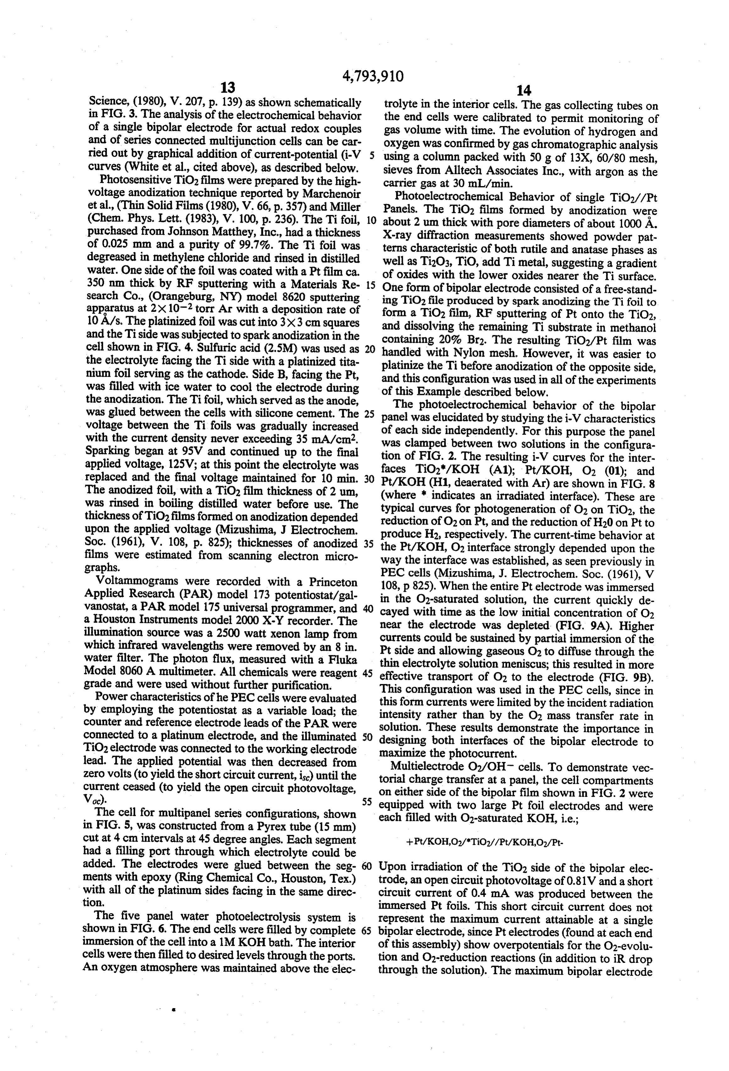
TiO2 electrode was connected to the working electrode maximize the photocurrent. lead. The applied potential was then decreased from Multielectrode O2/OH cells. To demonstrate vec zero volts (to yield the short circuit current, is) until the torial charge transfer at a panel, the cell compartments current ceased (to yield the open circuit photovoltage, on either side of the bipolar film shown in FIG. 2 were Voc). 55
The cell for multipanel series configurations, shown each filled with O2-saturated foil equipped with two large Pt
KOH, electrodes and were
in FIG. 5, was constructed from a Pyrex tube (15 mm) cut at 4 cm intervals at 45 degree angles. Each segment had a filling port through which electrolyte could be added. The electrodes were glued between the seg Upon irradiation of the TiO2 side of the bipolar elec ments with epoxy (Ring Chemical Co., Houston, Tex.) trode, an open circuit photovoltage of 0.81V and a short with all of the platinum sides facing in the same direc circuit current of 0.4 mA was produced between the tion. immersed Pt foils. This short circuit current does not The five panel water photoelectrolysis system is represent the maximum current attainable at a single shown in FIG. 6. The end cells were filled by complete 65 bipolar electrode, since Pt electrodes (found at each end immersion of the cell into a 1MKOH bath. The interior of this assembly) show overpotentials for the O2-evolu cells were then filled to desired levels through the ports. tion and O2-reduction reactions (in addition to iR drop An oxygen atmosphere was maintained above the elec through the solution). The maximum bipolar electrode
Page 17
current can be estimated by consideration of the A1 and cell for water splitting, a 5 panel cell, shown in FIG. 4, O1 i-V curves in FIG. 8. The short-circuit. photocur was illuminated for 5 h with a Xe lamp (266 mW/cm2 rent, isc, occurs where the cathodic and photoanodic incident). Gas evolution occurred at each end elec currents are equal (as indicated in FIG. 8 at the mixed trode, H2 being evolved on the Pt extreme and O2 at the potential, EM). The open circuit photovoltage TiO end. A volume of 0.52 mL of H2 (identified by gas (Voc=0.82V) is obtained as the potential difference chromatography evolved and an H2/O2 molar ration of when both currents are zero. 2.4/1 was obtained.
The predicted I-V curves for panels in series (FIG. 5) Vectorial charge transfer on bielectrode panels has are given in FIG. 10. These can be obtained by indepen been demonstrated. Means have been established for dent graphical addition of the cathodic curves by sum 10 coupling these panels to produce higher driving forces ming the potentials at constant current (since the elec trodes are connected in series) and, treating in the same than those available from systems with single semicon way, the anodic ones. The result of this procedure, in tics fromelectrodes ductor for predicting the PEC characteris individual i-V curves. The unassisted photo consideration of a two panel cell with both Pt cathodes lytic water splitting reaction has been demonstrated. No immersed in O2-saturated KOH, is shown in FIG. 10 as 15 curves A2 and O2. The power curves for the multiple effort was made in these studies to optimize the behav ior of the PEC cells through improvement of the TiO2 panels in series were obtained using the cell in FIG. 5. film,
Three panels were used with two intervening electro port. new interior redox couples, or better mass trans lyte solutions:
EXAMPLE 2
The present Example demonstrates the use of a small
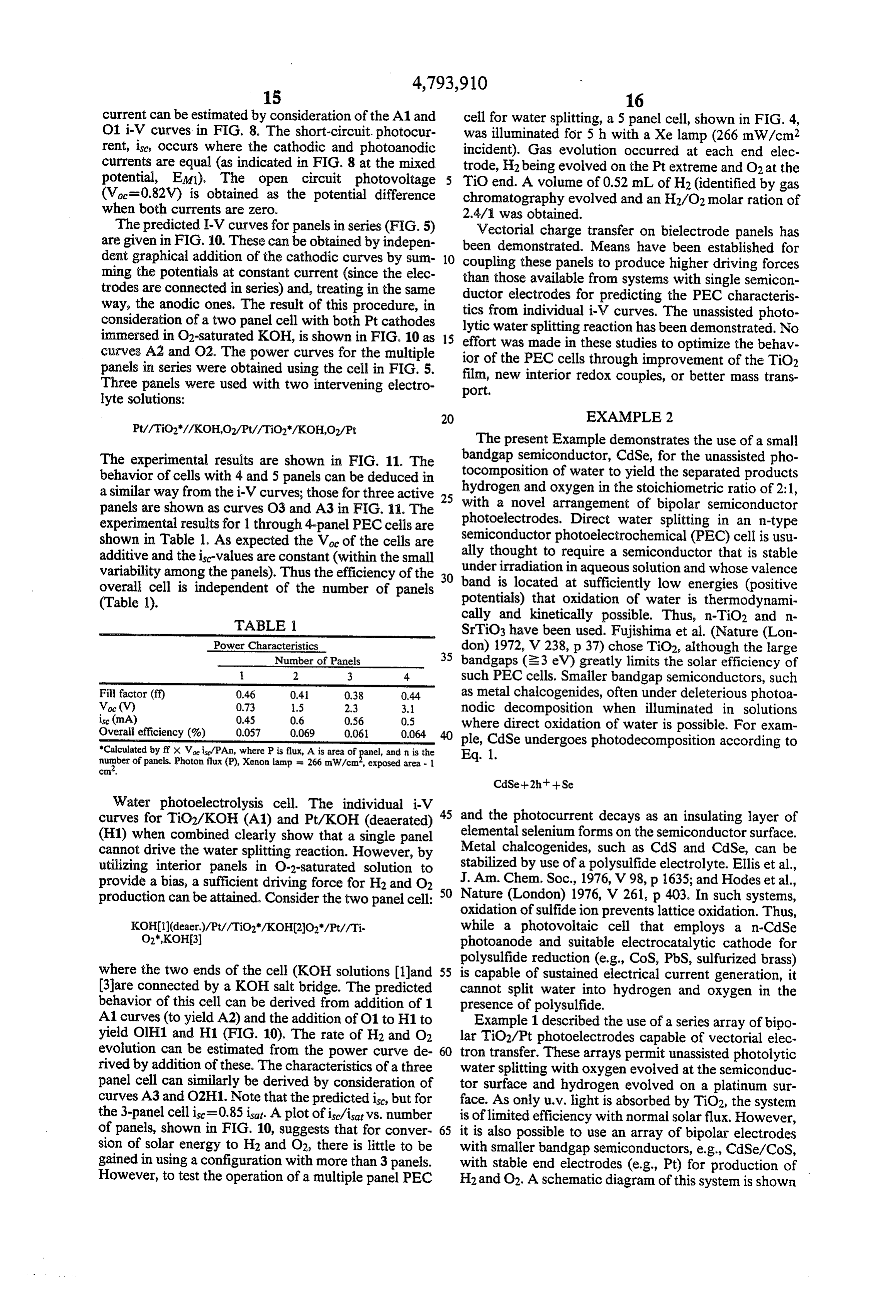
The experimental results are shown in FIG. 11. The bandgap semiconductor, CdSe, for the unassisted pho tocomposition of water to yield the separated products behavior of cells with 4 and 5 panels can be deduced in a similar way from the i-V curves; those for three active 25 hydrogen and oxygen in the stoichiometric ratio of 2:1, panels are shown as curves O3 and A3 in FIG. 11. The with a novel arrangement of bipolar semiconductor experimental results for 1 through 4-panel PEC cells are photoelectrodes. Direct water splitting in an n-type shown in Table 1. As expected the Voc of the cells are semiconductor photoelectrochemical (PEC) cell is usu additive and the isc-values are constant (within the small ally thought to require a semiconductor that is stable variability among the panels). Thus the efficiency of the 30 under irradiation in aqueous solution and whose valence overall cell is independent of the number of panels band is located at sufficiently low energies (positive (Table 1). potentials) that oxidation of water is thermodynami
TABLE 1.
cally and kinetically possible. Thus, n-TiO2 and n
SrTiO3 have been used. Fujishima et al. (Nature (Lon
Power Characteristics don) 1972, V 238, p. 37) chose TiO2, although the large 35 bandgaps (23 eV) greatly limits the solar efficiency of
Number of Panels 2 3 4. such PEC cells. Smaller bandgap semiconductors, such Fill factor (fi) 0.46 0.41 0.38 0.44 as metal chalcogenides, often under deleterious photoa
isc (mA)
nodic decomposition when illuminated in solutions
Overall efficiency (%) 0.057 0.069 0.061 0.064 where direct oxidation of water is possible. For exam "Calculated by fix Vis/PAn, where P is flux, A is area of panel, and n is the ple, CdSe undergoes photodecomposition according to nugber of panels. Photon flux (P), Xenon lamp = 266 mW/cm, exposed area - 1 Eq. 1.
Water photoelectrolysis cell. The individual i-V curves for TiO2/KOH (A1) and Pt/KOH (deaerated) 45 and the photocurrent decays as an insulating layer of (H1) when combined clearly show that a single panel elemental selenium forms on the semiconductor surface. cannot drive the water splitting reaction. However, by Metal chalcogenides, such as CdS and CdSe, can be utilizing interior panels in O-2-saturated solution to stabilized by use of a polysulfide electrolyte. Ellis et al., provide a bias, a sufficient driving force for H2 and O2 J. Am. Chem. Soc., 1976, V98, p 1635; and Hodes et al., production can be attained. Consider the two panel cell: 50 Nature (London) 1976, V 261, p. 403. In such systems, oxidation of sulfide ion prevents lattice oxidation. Thus,
KOH(1)(deaer.)/Pt//TiO2/KOH2O2/Pt//Ti while a photovoltaic cell that employs a n-CdSe O2,KOH(3) photoanode and suitable electrocatalytic cathode for polysulfide reduction (e.g., CoS, PbS, sulfurized brass) where the two ends of the cell (KOH solutions (1)and 55 is capable of sustained electrical current generation, it 3are connected by a KOH salt bridge. The predicted cannot split water into hydrogen and oxygen in the behavior of this cell can be derived from addition of 1 presence of polysulfide.
A1 curves (to yield A2) and the addition of O1 to H1 to Example 1 described the use of a series array of bipo yield Olh1 and H1 (FIG. 10). The rate of H2 and O2 lar TiO2/Pt photoelectrodes capable of vectorial elec evolution can be estimated from the power curve de 60 tron transfer. These arrays permit unassisted photolytic rived by addition of these. The characteristics of a three water splitting with oxygen evolved at the semiconduc panel cell can similarly be derived by consideration of tor surface and hydrogen evolved on a platinum sur curves A3 and O2H1. Note that the predicted isc, but for face. As only u,v. light is absorbed by TiO2, the system the 3-panel cell isc=0.85 isat. A plot of isc/isat vs. number is of limited efficiency with normal solar flux. However, of panels, shown in FIG. 10, suggests that for conver 65 it is also possible to use an array of bipolar electrodes sion of solar energy to H2 and O2, there is little to be with smaller bandgap semiconductors, e.g., CdSe/CoS, gained in using a configuration with more than 3 panels. with stable end electrodes (e.g., Pt) for production of However, to test the operation of a multiple panel PEC H2 and O2. A schematic diagram of this system is shown
Page 18
in FIG. 13. The energetics of vectorial electron transfer at one bipolar photoelectrode are illustrated in the ex panded view of the terminal photoelectrode, I/J, de where WL is the solar light flux incident on the cell, N picted in FIG. 13. The basic principles of PEC devices is the number of photopanels (6) and A is the projected have been discussed in detail. The chemical reactions area of a panel (the light flux is directed 45' off the pertaining to each interface are normal of the panels). If a correction is made for the absorption of light by the polysulfide solution, the effi
ciency is 5.3%. Hence, with the given quality of the e panels used here, improvements can be made in the
B, D, F, H. CoS/KOH (1 M), S (1 M), S22 + et S2 (dark) 10 system efficiency up to 5.3%.
Na2S (1 M) When the Pt faces were contacted by KOH and con C, E, G, I CdSe/KOH (1 M), S2 + hit D2- (light) nected by a KOH bridge, as shown in FIG. 13, hydro S (1 M) Na2S (1 M) gen and oxygen evolution occurred. The photovoltage
of the illuminated CdSe photoelectrode array induces 15 bipolarity in the dark electrode A/B. Water photolysis
CdSe thin films for PECs have been prepared by experiments were carried out for 1 h period without spray pyrolysis, vacuum evaporation, electrodeposi stirring. Upon illumination, bubbles immediately began tion, chemical bath deposition, and slurry painting (as streaming from the Pt surfaces. The identity of the gases described in Example 1). The bipolar electrodes used evolved at the Pt cathode and anode, hydrogen and here were fabricated by the method of Hodes et al. (J. 20 oxygen respectively, was verified by gas chromatogra Electrochem. Soc. (1980) V. 127, p 2252), by painting a phy. After 1 h, the rate of bubble formation on the slurry of CdSe on a titanium foil (0.025 mm thick) an terminal Pt surfaces decreased. This may have been nealing in air at 500 C. followed by photoannealing in caused by pH gradients developing at the Pt/KOH 0.1MH2SO4. Annealing in the absence of oxygen re interfaces. That degradation was not due to effects at sulted in panels with very poor open circuit voltages 25 the CdSe or CoS interfaces was verified by removing and short circuit currents. The beneficial effect of air the KOH bridge and obtaining power curves for electri annealing has been reported by others (Boudreau et al., cal generation. No decay was observed in the power J. Electrochem. Soc. (1986), V. 133, p. 1248). CoS was curves, hence decreased gas evolution was attributed to then electroplated on the back side of the titanium foil. phenomena in the terminal cells. Replacement of the The electrode (A,B) was made by sputter-depositing 30 solution bridge restored hydrogen evolution to the ini platinum on one side of titanium foil and electroplating tial rate (> 1 cm/h), supporting the above conclusion. CoS on the opposite side. The terminal photoelectrode The hydrogen to oxygen volume ratio obtained in this (I,J) was made by painting and annealing a slurry of study was 2.1-0.3. The efficiency (calculated for light CdSe on titanium foil which had been previously sput incident on the cell) for water photolysis, calculated by ter-deposited with Pt on the opposite side. 35 Eq. 3, was 0.32%.
All CdSe semiconductors in the array were in contact with a stabilizing polysulfide solution and only the two terminal Pt electrodes contacted 2M KOH and were connected to each other by a KOH salt bridge. Oxygen where R is the rate of hydrogen evolution (mol/s), and was evolved at the Pt face of the Pt/CoS electrode G' is the standard free energy change for the decompo while hydrogen was evolved at the Pt face of the sition of water to hydrogen and oxygen (J/mol). If a CdSe/Ptelectrode. The relevant current-potential (i-V) correction is made for the light absorbed by the polysul data for a CdSe/CoS panel are shown in FIG. 14. fide solution, the efficiency was 0.91%. Further im Curve A is the i-V characteristic for the dark reduction provements can be made by using a better electrode of polysulfide of the CoS electrodes. The photooxida 45 with a lower overpotential for O2 evolution then Pt tion of sulfide on the semiconductor surface is shown on (e.g., a nickel based electrode (Tidak et al., Comprehen curve B. The open circuit voltage, Voc, is 0.5V with a sive Treatise of Electrochemistry, Bockris, J. O'M., ed., short circuit current, isc, indicated by the dotted line Plenum Press: N.Y. (1981), pp. 13-33.) and by using placed so that the magnitude of the anodic current smaller bandgap material either directly or as underlay (curve B) is equal in magnitude to the cathodic current 50 ers for larger bandgap materials in biphotonic tandem (curve A) of 12 mA/cm2. panels. (Weber, et al., J. Electrochem. Soc., (1984) The power characteristics of a six photoelectrode 1331:1258).
PEC array were evaluated by employing a Princeton Changes may be made in the construction, operation applied Research (PAR) model 173 potentiostat/gal and arrangement of the various parts, elements, steps vanostat with a PAR model 175 universal programmer 55 and procedures described herein without departing as a variable load. The potential of a CdSe surface from the concept and scope of the invention as defined under illumination with a xenon lamp, was adjusted in the following claims.
from zero volts relative to a CoS electrode (to yield is) What is claimed is:
to negative potentials, until the current ceased (to yield 1. A multielectrode photoelectrochemical unit for the V). The results are shown in the inset of FIG. 14. 60 unassisted photoelectrical-induction of a chemical reac As with the TiO2 system, the open circuit photovolt tion comprising:
ages are additive, the sum of the series being in excess of a housing having at least one light-passing side, a first 1.5V. At higher light fluxes the open circuit voltage of end, a second end and a housing wall defining an a single panel was in excess of 0.6V. internal section;
The fill factor, ff, for the series array was 0.57. The 65 a first photoactive bipolar electrode panel in the in efficiency for electrical power generation measured for ternal section, said first photoactive bipolar elec six photoelectrode panels calculated by Eq. 2 was 1.9%. trode panel having a semiconductor side, an ohmic contact layer and a underside and being attached to
Page 19
the housing wall near the first end of said internal 5. The multielectrode photoelectrochemical unit of section with the semiconductor side oriented claim 1 or 2 wherein at least one terminal compartment toward the first end and partially forming a first comprises a means for collecting a gaseous pnotode terminal compartment; and composition product.
a second photoactive bipolar electrode panel in the 5 6. The multielectrode photoelectrochemical unit of internal section, said second photoactive bipolar claim 1 or 2 wherein the catalytic side and underside electrode panel having a semiconductor side, an comprise platinum, ruthenium dioxide or cobalt sulfide. ohmic contact layer and a catalytic side and being 7. A multielectrode photoelectrochemical unit for attached to the housing wall near the second end of unassisted photoelectrical-induction of a chemical reac the internal section with the catalytic side oriented 10 tion comprising:
toward the second end and partially forming a a housing having at least one light-passing side, the second terminal compartment, an internal compart housing having a first end, a second end and a ment in said internal section being partially formed housing wall defining an internal section; by the underside of the first photoactive bipolar a first exterior bipolar electrode panel attached to the electrode panel and the semiconductor side of the housing wall near the first end of the internal sec tion of the housing, said first exterior bipolar elec second photoactive bipolar electrode panel, said first and second photoactive bipolar electrode pan trode panel having a gas-evolving side oriented els being attached to said housing walls to prevent toward the first end and partially forming a first liquid flow between the internal compartment and 20 terminal compartment, an ohmic contact layer and the terminal compartments and being positioned so an underside;
that light from an external source entering the a second exterior bipolar electrode panel attached to internal section is substantially incident upon the the housing wall near the second end of the hous semiconductor sides. ing said second bipolar electrode panel having a 2. A multielectrode photoelectrochemical unit for gas-evolving side oriented toward the second end unassisted photoelectrical-induction of a chemical reac 25 and partially forming a second terminal compart tion comprising: ment, an ohmic contact layer and a semiconductor a housing having at least one light-passing side, a first side;
end, a second end and a housing wall defining an at least one interior bipolar electrode panel, said inte internal section; rior bipolar electrode panel having a semiconduc a first photoactive bipolar electrode panel in the in 30 tor side, an ohmic contact layer and an underside and being attached to the housing wall in the inter ternal section, said first photoactive bipolar elec nal section between the exterior bipolar electrode trode panel having a semiconductor side, an ohmic panels, said internal section being divided by inter contact layer and an underside and being attached nal and exterior bipolar electrode panels into at to the inside of the housing wall near the first end is least two internal compartments; and of said internal section to physically separate the means for collecting evolved gaseous photodecom internal section on each side of the first photoactive position products in at least one terminal compart bipolar electrode panel with the semiconductor ment.
side oriented toward the first end and partially 8. A multielectrode photoelectrochemical unit for forming a first terminal compartment; and a second photoactive bipolar electrode panel in the 40 tion unassisted photoelectrical-induction of a chemical reac comprising:
internal section, said second photoactive bipolar a housing having at least one light-passing side, the electrode panel having a semiconductor side, an housing having a first end, a second end and a ohmic contact layer and a catalytic side and being housing wall defining an internal section; attached to the inside of the housing wall near the 45 a first exterior bipolar electrode panel attached to the second end of the internal section to physically separate the internal section on each side of the inside of the housing wall near the first end of the second photoactive bipolar electrode panel with internal section of the housing to physically sepa rate the internal section on each side of the first the catalytic side oriented toward the second end exterior bipolar electrode panel, said first exterior and partially forming a second terminal compart- 50 bipolar electrode panel having a gas-evolving side ment, an internal compartment in said internal sec oriented toward the first end and partially forming tion formed by the housing wall, the underside of a first terminal compartment, an ohmic contact the first photoactive bipolar electrode panel and layer and an underside;
the semiconductor side of the second photoactive a second exterior bipolar electrode panel attached to bipolar electrode panel, said first and second pho- 55 the inside of the housing wall near the second end toactive bipolar electrode panels being attached to of the housing to physically separate the internal said housing walls to prevent liquid flow between section on each side of the second exterior bipolar the internal compartment and the terminal com electrode panel, said second bipolar electrode partments and being positioned so that light from panel having a gas-evolving side oriented toward an external source entering the internal section is 60 the second end and partially forming a second substantially incident upon the semiconductor terminal compartment, an ohmic contact layer and sides. a semiconductor side;
3. The multielectrode photoelectrochemical unit of at least one interior bipolar electrode panel, said inte claim 1 or 2 wherein the semiconductor side comprises rior bipolar electrode panel having a semiconduc a p-type semiconductor or a n-type semiconductor. 65 tor side, an ohmic contact layer and an underside 4. The multielectrode photoelectrochemical unit of and being attached to the inside of the housing wall claim 1 or 2 wherein the internal compartment com in the internal section between the exterior bipolar prises a closable port in the wall of the housing. electrode panels, said internal section being divided
Page 20
by internal and exterior bipolar electrode panels 15. The multielectrode photoelectrochemical unit of into at least two internal compartments; and claim 7 or 8 wherein the semiconductor side comprises means for collecting gaseous photodecomposition a p-type or n-type semiconductor.
products from at least one terminal compartment. 16. The multielectrode photoelectrochemical unit of 9. The multielectrode photoelectrochemical unit of 5 claim 7 or 8 wherein the semiconductor side comprises claim 7 or 8 wherein the bipolar electrode panels having a metal chalcogenide.
a semiconductor side are oriented so that light from an 17. The multielectrode photoelectrochemical unit of claim external source passing into the internal section is sub cadmium 7 or 8 wherein the semiconductor side comprises stantially incident upon a majority of the semiconductor 10 18. Theselenide or cadmium sulfide. multielectrode photoelectrochemical unit of sides.
claim 7 or 8 wherein the gas-evolving sides comprise 10. The multielectrode photoelectrochemical unit of platinum.
claim 7 or 8 wherein the gas-evolving side of the first 19. The multielectrode photoelectrochemical unit of exterior bipolar electrode panel and the gas-evolving claim 7 or 8 wherein the undersides comprise cobalt side of the second exterior bipolar electrode panel are 15 sulfide, lead sulfide or sulfurized brass. metallic. 20. The multielectrode photoelectrochemical unit of 11. The multielectrode photoelectrochemical unit of claim 7 or 8 wherein the ohmic contact layers comprise claim 7 or 8 wherein there are three interior bipolar a metal foil.
electrode panels. 21. The multielectrode photoelectrochemical unit of 12. The multielectrode photoelectrochemical unit of 20 claim 7 or 8 wherein the ohmic contact layers comprise claim 7 or 8 wherein the internal compartments are a titanium foil.
defined further as each having a housing wall and two 22. The multielectrode photoelectrochemical unit of ends, each end consisting of a side of a bipolar electrode claim 7 or 8 wherein the ohmic contact layers comprise panel. a metallic foil, the semiconductor sides comprise a metal 13. The multielectrode photoelectrochemical unit of 25 leadchalcogenide, the undersides comprise cobalt sulfide, claim 7 or 8 wherein the internal compartments com comprise sulfide or sulfurized brass, the gas-evolving sides platinum and the internal compartments are prise closable filling ports usable for transfer of fluids to defined further and from the compartments. as being substantially filled with a fluid polysulfide electrolyte.
14. The multielectrode photoelectrochemical unit of 30 23. The multielectrode photoelectrochemical unit of claim 13 wherein the closable filling parts are sealed to claim 7 or 8 wherein the photoelectrically-induced isolate internal compartments during immersion of the chemical reaction is the decomposition of water to O2 multielectrode photoelectrochemical unit in an electro and H2.
lyte bath. a
Provenance
- Collection
- Cited prior art
- Original PDF
- patentimages.storage.googleapis.com →
- Filed
- 1987-05-18
- Pages
- 20
- Method
- pdftotext (the PDF's own text layer) + pdftoppm 300dpi page scans
- Source
- Google Patents bibliographic record
- Granted
- 1988-12-27
- Inventors
- Eugene Smotkin; Allen J. Bard; Marye A. Fox; GTI Energy
- Transcribed from
- patentimages.storage.googleapis.com →