patent · US4760421
Graphic printing device including a fiber optic bundle with electronic means for providing coherence
26 July 1988
Page 1 — bibliographic record
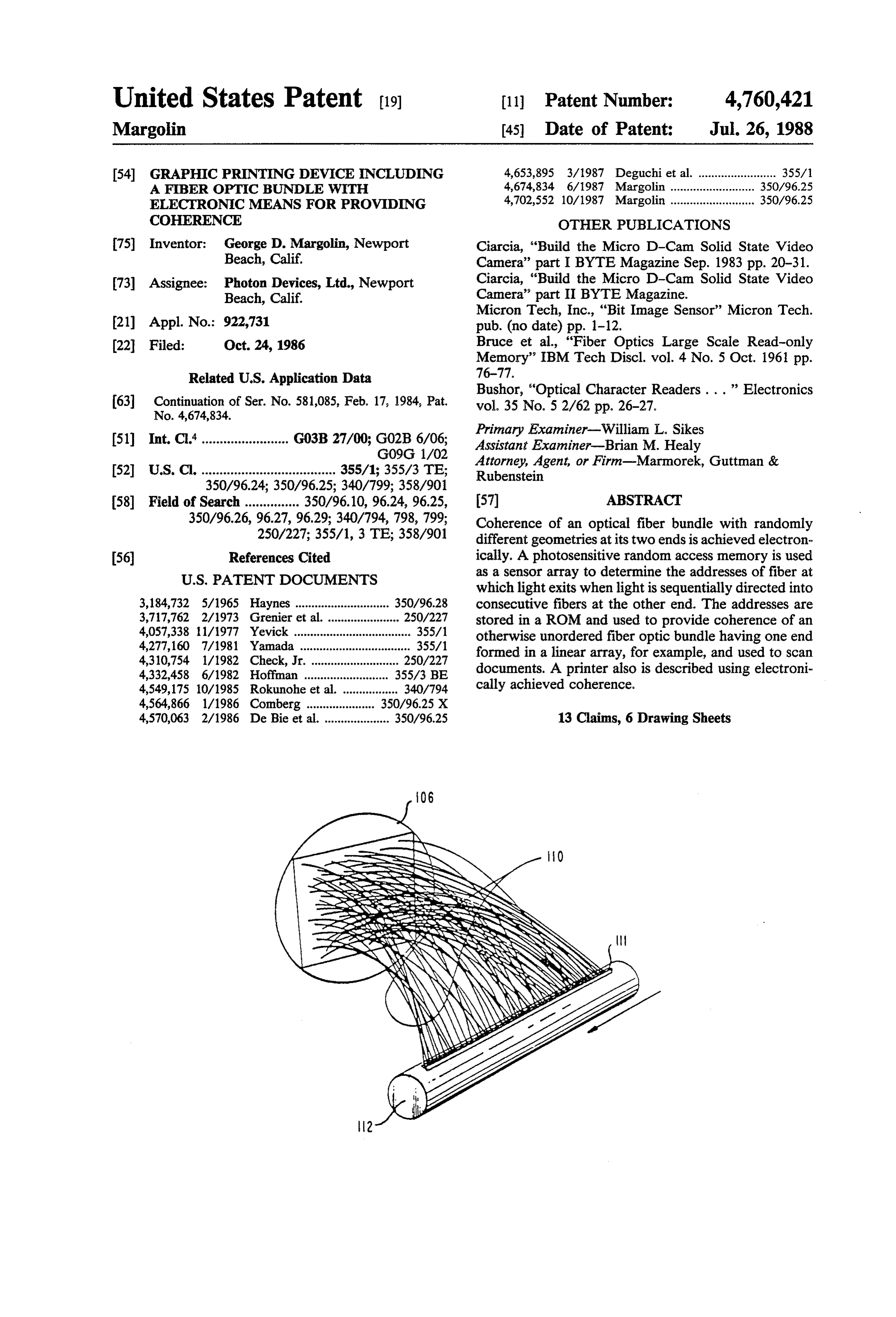
United States Patent (19) 11 Patent Number: 4,760,421 Margolin (45. Date of Patent: Jul. 26, 1988 54 GRAPHIC PRINTING DEVICE INCLUDING 4,653,895 3/1987 Deguchi et al. ........................ 355/1 AFBER OPTC BUNDLE WITH 4,674,834 6/1987 Margolin .......................... 350/96.25 ELECTRONIC MEANS FOR PROVIDING 4,702,552 10/1987 Margolin .......................... 350/96.25 COHERENCE OTHER PUBLICATIONS 75 Inventor: George D. Margolin, Newport Ciarcia, "Build the Micro D-Cam Solid State Video Beach, Calif. Camera' part I BYTE Magazine Sep. 1983 pp. 20-31. 73 Assignee: Photon Devices, Ltd., Newport Ciarcia, "Build the Micro D-Cam Solid State Video Beach, Calif. Camera' part II BYTE Magazine.
Micron Tech, Inc., “Bit Image Sensor' Micron Tech.
21 Appl. No.: 922,731 pub. (no date) pp. 1-12.
22 Filed: Oct. 24, 1986 Bruce et al., “Fiber Optics Large Scale Read-only Memory” IBM Tech Discl. vol. 4 No. 5 Oct. 1961 pp.
Related U.S. Application Data 76-77.
Bushor, "Optical Character Readers . . .” Electronics 63 Continuation of Ser. No. 581,085, Feb. 17, 1984, Pat. vol. 35 No. 5 2/62 pp. 26-27.
Primary Examiner-William L. Sikes 51) Int. Cl......................... G03B 27/00; G02B6/06; Assistant Examiner-Brian M. Healy G09G 1/02 Attorney, Agent, or Firm-Marmorek, Guttman & 52 U.S. Cl. ..................................... 355/1; 355/3 TE; Rubenstein
58) Field of Search ............... 350/96.10, 96.24, 96.25, 57 ABSTRACT 350/96,26,96.27, 96.29; 340/794, 798, 799; Coherence of an optical fiber bundle with randomly 250/227; 355/1, 3 TE, 358/901 different geometries at its two ends is achieved electron 56 References Cited ically. A photosensitive random access memory is used
which light exits when light is sequentially directed into 3,184,732 5/1965 Haynes ............................. 350/96.28 consecutive fibers at the other end. The addresses are 3,717,762 2/1973 Grenier et al. stored in a ROM and used to provide coherence of an 4,057,338 11/1977 Yevick ... otherwise unordered fiber optic bundle having one end 4,277,160 7/1981 Yamada ..... formed in a linear array, for example, and used to scan 4,310,754 l/1982 Check, Jr. ........................... 250/227 documents. A printer also is described using electroni
4,549,175 10/1985 Rokunohe et al. ................. 340/794 cally achieved coherence.
4,564,866 l/1986 Comberg ........... ... 350/96.25 X 4,570,063 2/1986 De Bie et al. .................... 350/96.25 13 Claims, 6 Drawing Sheets
Page 2
Drawing sheet — no readable text.
Page 3
Drawing sheet — no readable text.
Page 4
Drawing sheet — no readable text.
Page 5
Drawing sheet — no readable text.
Page 6
Drawing sheet — no readable text.
Page 7
Drawing sheet — no readable text.
Page 8
a bundle of so many fibers of such small size is difficult
GRAPHIC PRINTING DEVICE INCLUDING A to achieve and, therefore, costly.
FIBER OPTIC BUNDLE WITH ELECTRONIC
MEANS FOR PROVIDING COHERENCE DISCLOSURE OF THE INVENTION An inexpensive graphics input or output device is
REFERENCE TO RELATED PATENT achieved in a preferred embodiment by employing a APPLICATION bundle of optical fibers and a random access memory The present patent application is a continuation of my a(RAM) which is adapted for sensing light signals. Such co-pending patent application Ser. No. 581,085, now 10 is memory is available commercially, is inexpensive and U.S. Pat. No. 4,674,834, filed Feb. 17, 1984, entitled the fibers is be known to useful to sense light signals. One end of constrained to form a linear array which “Graphic Input/Output Device With Fiber Optic Bun can be used, for dle Having Electronic Means For Providing Coher end of the arrayexample, to scan a document. The other ence', and assigned to the assignee of the present patent bundle, at random.isThe merely gathered into at least one only constraint on the bundled application. 15 end is that the cross sectional area of the bundle is con REFERENCE TO THE APPENDICES figured to correspond generally with the area of the Reference is made to the magazine articles Build the photosensitive RAM.
In this embodiment the diameter of each fiber is
Micro D-Can Solid-State Video Camera. Part I, Byte chosen to be large compared to the area of a bit location Magazine, September 1983, pp. 20-31, and Part II, in 20 in the RAM. As a result, a plurality of RAM memory Byte Magazine, October, 1983, pp. 67-86, copies of bits is positioned to correspond to a single pixel (Picture which are appended hereto Appendix I and incorpo Element). Moreover, rated herein by reference. Reference is also made to a 12 be large (approximatelythe3000) number of fibers is chosen to compared to the number page product description entitled Micron Technology. of pixels required for satisfactory optical definition. Inc. IS32 Optic RAM. 32,768 Bit Image Sensor, also 25 Consequently the input at the linear end of the array of appended hereto, as Appendix II and incorporated fibers comprises 3000 signals and so provides high reso herein by reference. Appendix II describes the charac lution, yet the signals at the sensor array end are of teristics of the IS32 Optic RAM, and gives both sup relatively low density compared to the density (64,000) plier information and a description of addressing cir of the available addressable memory locations in the cuits. 30 sensor RAM. In this manner tolerances may be relaxed TECHNICAL FIELD and costs reduced even though resolution is high. For This invention relates to graphics input or output input example, if two mil diameter fibers are used, the linear devices and more particularly to such a device includ sand fibers array will have a density of more than three thou ing a fiber optic bundle. over, say the width of a 8.5 inch letter size 35 document. The output end could, in this example, be
BACKGROUND ART bundled into a rectangle of approximately 217X92 mils, Graphics input or output devices are well known in which would perfectly match a commercially available 64K Photosensitive RAM. This RAM can be purchased the art. One such device employing a linear array of in OEM quantities for about $4.00, a price far lower photodiode sensors is commercially available from 40 than any other high density photosensitive device on "Reticon' of Sunnyvale, Calif.
This array of photodiodes is positioned so that light the3000 market today. Since the bundle of approximately fibers is physically abutted or optically focussed impinging upon a document to be copied forms an against the sensor RAM, each fiber corresponds to an image on the array through a suitable lens system. The area of the RAM occupying the space of about twenty document is moved by a control mechanism which 45 addressable memory locations.
synchronously strobes the array to provide signals rep Coherence is preserved in this embodiment by em resentative of the linear image segment being scanned. ploying a Look-up Table which can be incorporated A problem with this type of arrangement is that a into a computer program or embodied in a Programma considerable distance is required between the array and ble Read Only Memory (PROM) in a conventional the document in order to reduce the scanned image to a 50 manner. The Look-up Table records the correspon size compatible with the minute size of the array. Fur dence between the position of each fiter in the linear ther, all the sensors have to be perfect and the signals input end and one of its associated addresses in the provided by the array require additional means to store RAM to which it couples at the bundled end. The cor and convert the signals to digital form. respondence is determined upon manufacture by pass Graphic devices are known which employ fiber optic 55 ing light through a narrow slit (smaller than the diame bundles to permit segments of a scanned image to be ter of each fiber), which is oriented transversely to the applied to minute sensor arrays without the consider linear array and is moved across the fibers of the array able distance previously required. The signal output of sequentially. As the slit passes each fiber, the corre such a fiber optic bundle still requires conversion to sponding illuminated RAM addresses are noted, and digital form and the fiberbundle has to provide physical 60 one address is chosen. The correspondence thus estab coherence between the input and output (picture ele lished is stored in a bit map, which may be recorded ments or pixels) such that the relationships between the permanently in, for example, a PROM. Once the bit signals at the input ends of the fibers and at the output map is stored, the system is initialized for later use. ends of fibers are identical. The term "physical coher Alternatively, the correspondence may be determined ence' means that those relationships are maintained 65 in the absence of a permanent built-in bit map by initial physically by keeping the fibers at the output end in a izing the system each time the system is used, or, by predetermined physical relationship with respect to the using a computer program containing the Look-up Ta fibers at the input end. The requirement of coherence in ble.
Page 9
The device can be used to scan a document for fac process. The side 20 includes a slit 21 which, for exam simile or for intelligent copier applications, as de ple, may be formed in an opaque film or tape 23 which scribed, or in a reverse mode by coupling an imaging is moved along an axis, represented by double headed display to the bundled end, and by generating an image arrow X in FIGS. 1 and 2, in a manner to expose the on the face of the display, in accordance with a bit map fibers of the linear array at end 12, in sequence, to light. generated during initialization. In the printer embodi This causes the illumination of a sequence of bit loca ment the linear end may be abutted against a xero tions in (sensor) RAM 17 of FIG. 3, corresponding to graphic drum for selective discharge of linear segments the sequence of fibers illuminated in the linear array. of the drum as the drum rotates. The scanner, the Slit 21 is narrow (less than a fiber diameter) and is pro printer, or both may be attached to a computer, such as O gressively moved along the linear array in synchronism a personal computer, having sufficient bit processing with the interrogation of the RAM 17, so that the bit capability to provide facsimile or intelligent copier op map of each fiber is individually read out and recorded. eration with relatively little adaptation. The arrangement for moving slit 21 as required may be BRIEF DESCRIPTION OF THE DRAWINGS 15 any convenient translation mechanism suitable for this purpose, and a detailed discussion of such an arrange
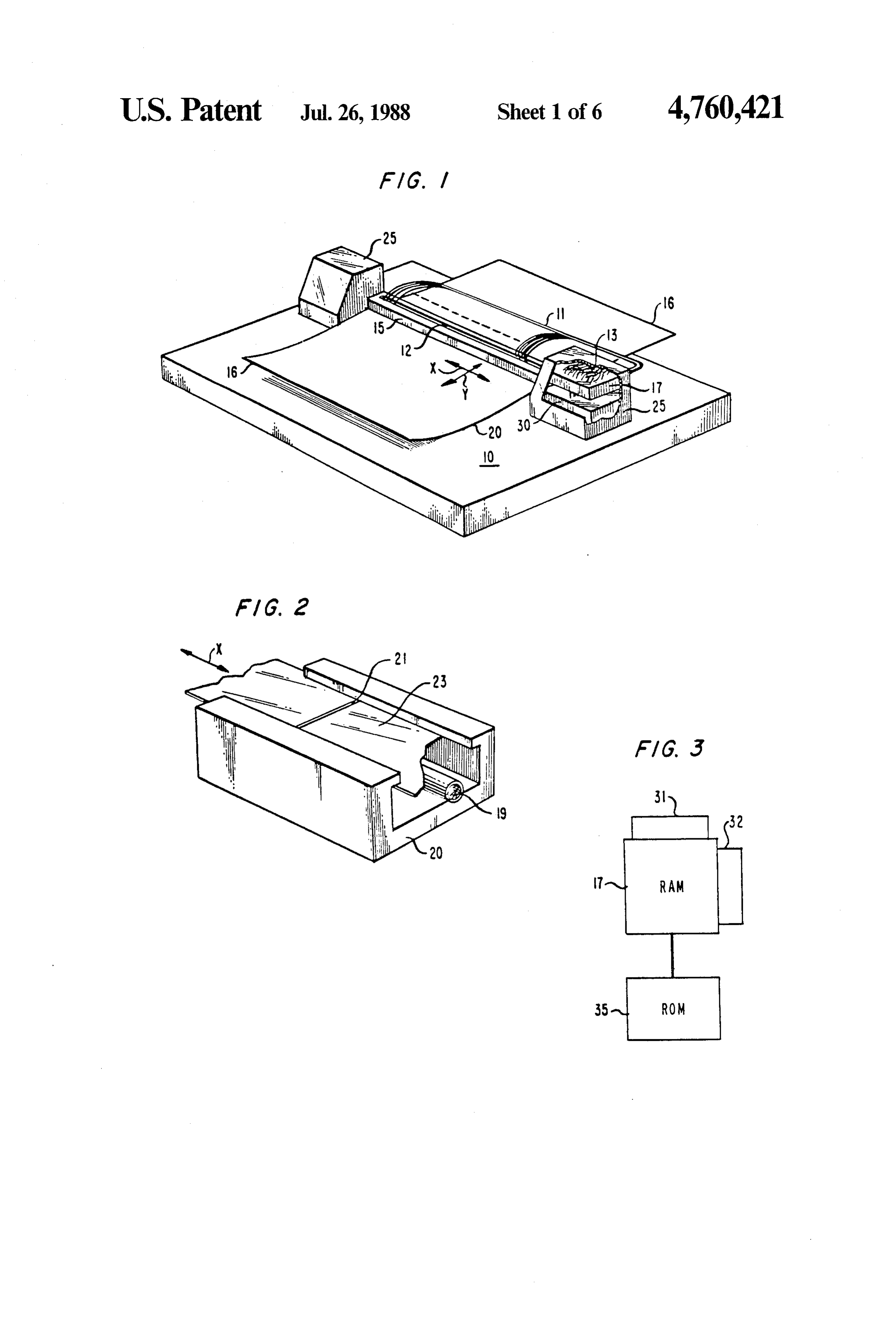
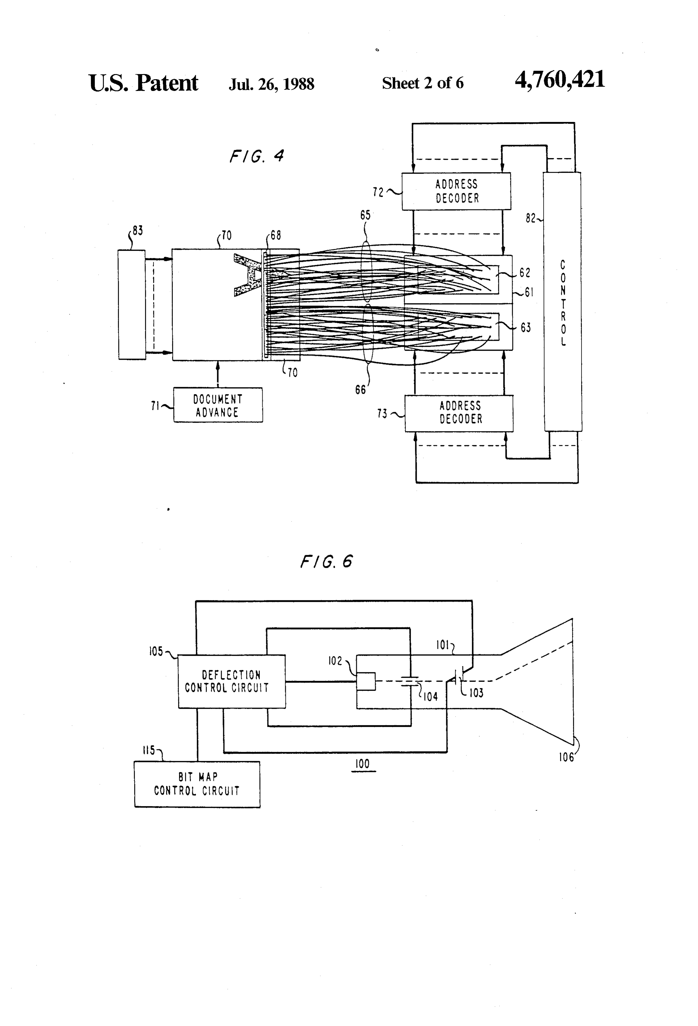
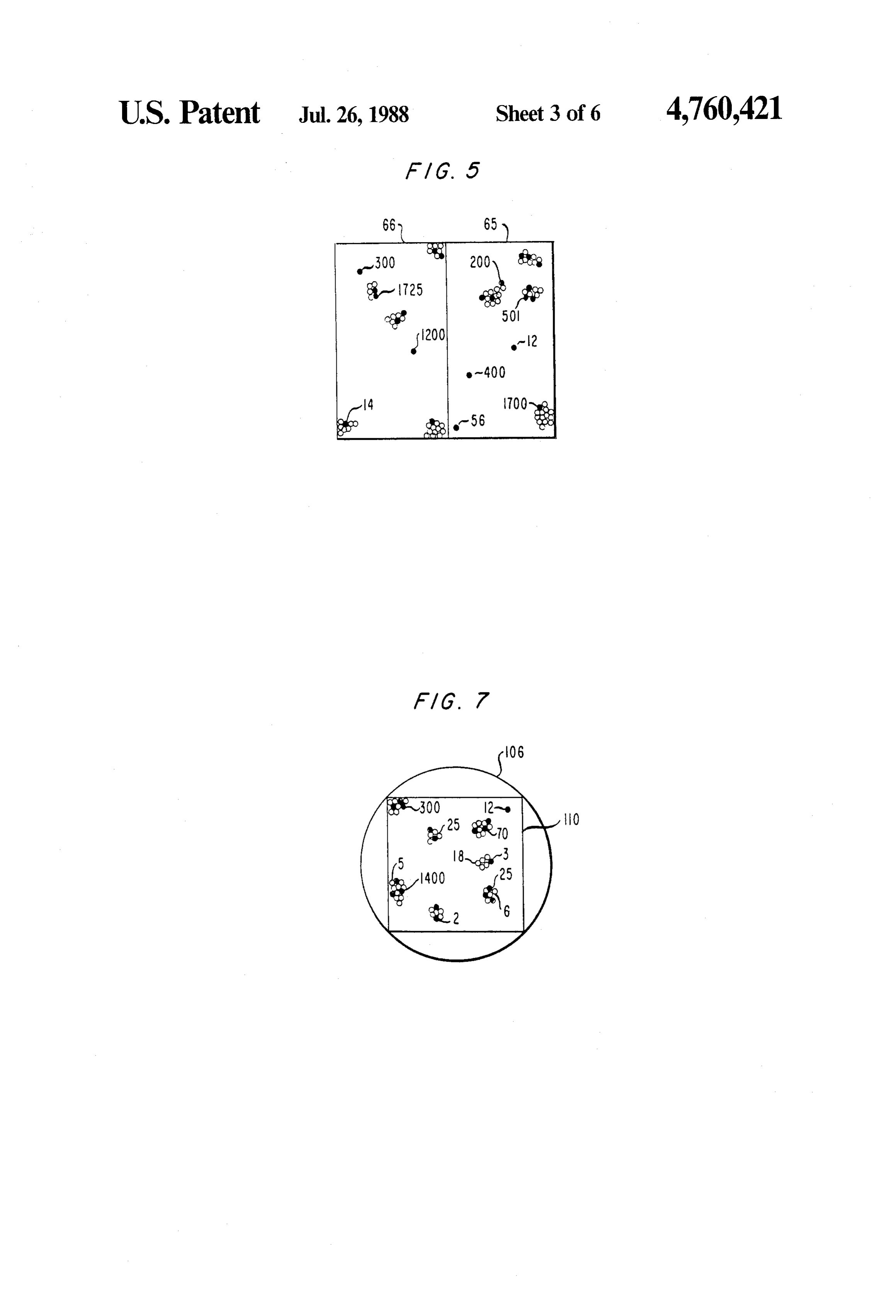
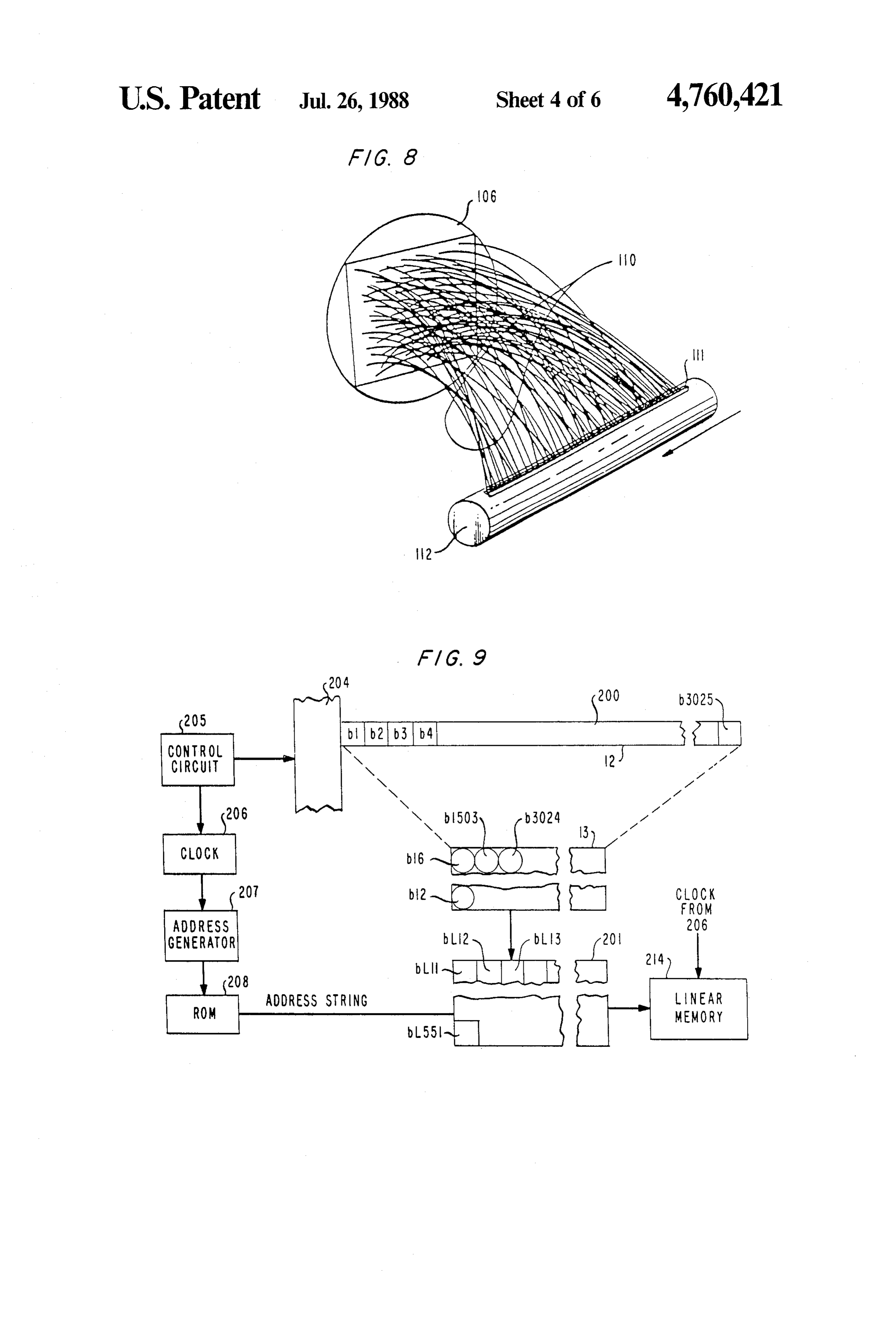
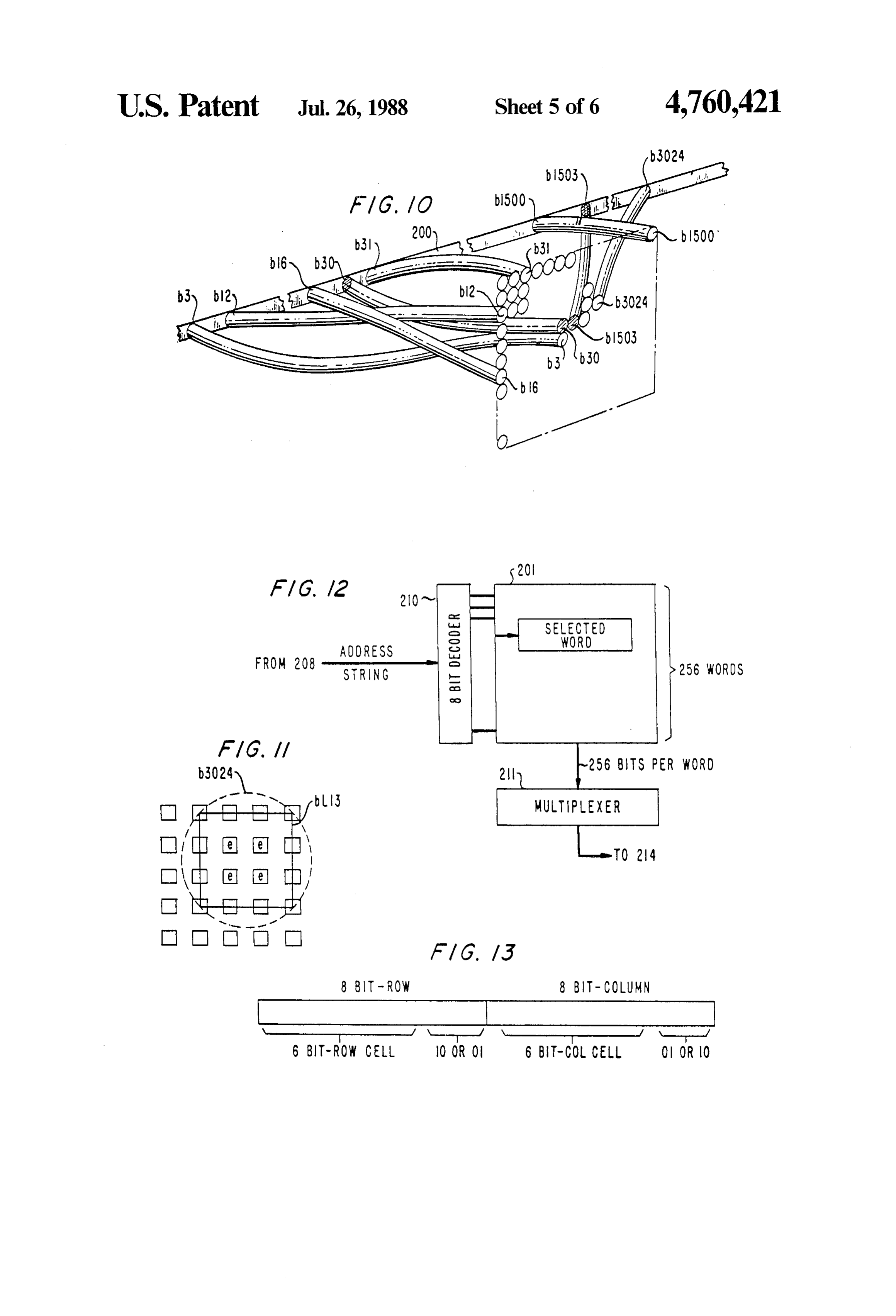
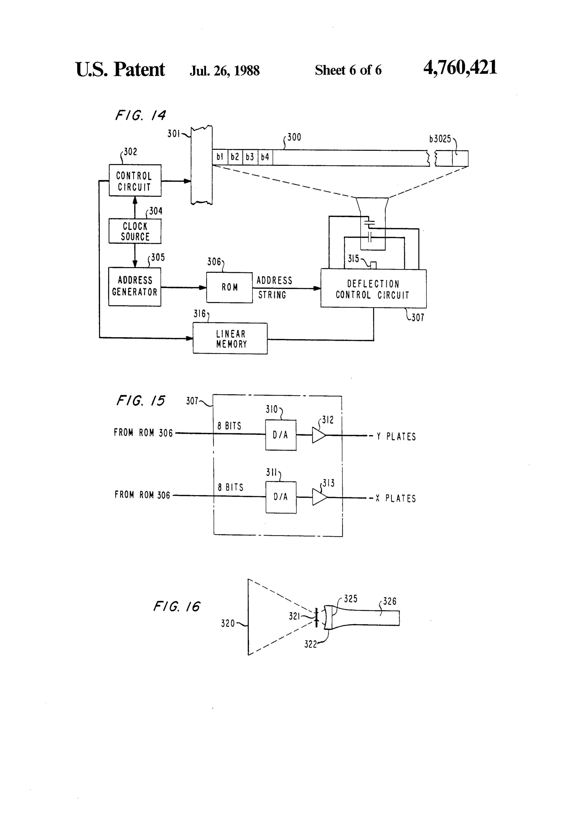
FIGS. 1, 4, 9, and 14 are schematic representations of ment is not necessary for an understanding of this inven systems in accordance with this invention. tion. All that is necessary is that a slit be passed along FIG. 2 is a schematic representation of a portion of an the fiber ends at 12 to illuminate the fibers in sequence initializing apparatus in accordance with this invention. to establish an appropriate Look-up Table or Bit Map FIG. 3 is a schematic representation of a portion of 20 during an initialization procedure. A suitable control the system in FIG. 1. circuit for controlling the movement of slit 21 and for FIG. 5 is a schematic representation of a random controlling source 19 is represented by circuit board 30 distribution of light signals in a non-coherent fiber bun in FIG. 1. The apparatus to accomplish initialization dle. can be included as part of the apparatus of FIG. 1, or FIGS. 6, 7, and 8 are schematic representations of 25 may be a separate dedicated fixture as shown in FIG. 2. portions of a graphic printer in accordance with this RAM 17 includes X and Y address decoders 31 and invention. 32 in a familiar manner as indicated in FIG. 3. All bit FIGS. 10, 11, and 12 are schematic representations of locations in the RAM are initialized or precharged prior portions of the scanner arrangement of FIG. 9. to each "interrogation' cycle, in which all bits are inter FIG. 13 is a schematic representation of the address 30 rogated to determine which address was illuminated ing organization for blocks of bit locations in RAM in when light enters the next consecutive fiber during the the systems of FIGS. 1, 4, 9, or 14; and initialization process. Specifically, incident light dis FIGS. 15 and 16 are schematic representations of the charges the bit location (or locations) of the RAM cor system of FIG. 14. responding to the fiber at end 12 which is illuminated at 35 any given instant during the initialization process. The
DETAILED DESCRIPTION RAM is then interrogated and the address (or ad FIG. 1 shows an illustrative portable graphics input dresses) of the discharged bit location (or locations) is device 10 in accordance with one aspect of this inven stored in the Look-up Table or Read Only memory tion. The device comprises an optical fiber bundle 11 (ROM) 35 under the control of control circuit 30 of having first and second ends 12 and 13 respectively. FIG. 1. At the termination of the initialization process, The ends of the fibers at 12 are constrained, by ferrule the addresses of all the consecutively discharged bit 15 into a linear array positioned for scanning successive locations of RAM 17 are stored. This procedure estab linear segments or lines of an image when moved with lishes the coherence between the randomly gathered respect to a document i6, for example, along an axis fiber ends at 13 and the linear arrangement of fiber ends aligned with double-headed arrow Y. 45 at 12. The system is now ready for operation. The ends of the fibers at 13 are not organized, but As noted, each fiber, preferably, is larger in diameter rather are gathered and bunched randomly, and fused. than the area occupied by a group of bit locations in the The fused bundle is abutted physically or focussed opti (sensor) RAM. This relationship ensures that at least cally onto the surface of Random Access Memory one unambiguous bit location in the sensor RAM will be (RAM) 17. The diameter of each fiber is chosen to be 50 illuminated during each interrogation cycle, and that a large compared to the area of a bit location in the RAM, defect in the RAM will not cause loss of information. so that twenty or so bits of the RAM correspond to The redundancy of about 10 to 20 bit locations, corre each fiber at end 13. The choice of size ensures that any sponding to a single fiber, was selected for convenience light entering a fiber at end 12 impinges at least one because of the economy and availability of 64K RAMs, useable bit location of the RAM when it exits at end 13. 55 and the excellent resolution, economy and general util Coherence, that is, the ordered relationship, between ity of the device using 2 mil fibers. Practical conse the light signals entering the linear array offibers at end quences of this choice will be discussed below, in rela 12 and light exiting the fibers at the bundled end 13 is tion to FIGS. 9 and 11. A lower level of redundancy provided by storing, in a Look-up Table in a computer, may be chosen, without sacrificing required resolution or by a Programmable Read Only memory (PROM), 60 by varying the RAM size or geometry, the fiber size, or the address of a bit location in RAM 17 which senses other characteristics.
light exiting a particular fiber at end 13 as light is di A suitable sensor RAM for the embodiment disclosed rected into each of the fibers at end 12 in sequence. is available commercially from Micron Technology Initialization of an embodiment such as that shown in Inc., of Boise, Id. The RAM is divided into two sec FIG. 1 is illustrated by the apparatus of FIGS. 2 and 3. 65 tions, each 256 by 128 cells. Accordingly, it is conve The apparatus, includes a light source 19 enclosed by nient in the illustrative embodiment to divide the fibers housing 20. A side of housing 20 in FIG. 2, is placed at end 13 into two arrays to associate with the two adjacent to ends 12 of FIG. 1 during an initialization sections of the RAM if the Micron Technologies RAM
Page 10
is used. Appendix II describes in detail the address vision for illumination may correspond to that provided structure of the Micron Technology IS32 Optic RAM in any familiar copier. The illumination means is repre and circuitry for its use. For speed of operation, it may sented by block 83 in FIG. 4.
be desirable to divide the fibers into a greater number of The following Table represents a Look-up Table or arrays to reduce the addressing requirements. 5 Bit map for an illustrative six fibers. It should be clear A complete system for entering graphics information that the operation of the RAM interrogation according into a computer using such a sensor RAM is disclosed in to the Look-up Table during each scan period is entirely detail in the September 1983 issue of Byte Magazine at consistent with the operation described in the above pp. 20-31, the computer interfaces and control software mentioned publications. But the results are considerably for the system are described in the October issue of that O different because the optical input received by the same publication at pp. 67-86. These two articles are RAM during each interrogation is effectively a ran attached hereto as Appendix I, and are hereby incorpo domly dissected linear input distributed over the entire rated by reference and made of record. The present (sensor) RAM-instead of a line from the array being invention can be used with the system described in laid out on a line of the sensor, as it would be in the case those publications, by providing, in addition, the herein 15 of a direct lens projected image. It is clear that resolu described fiber optic array, a sensor array, and a mem tion is significantly improved.
ory for storing a Look-up Table or Bit Map.
FIG. 4 shows schematically an arrangement of the type shown in FIGS. 1 and 3 for use with the system of Look-up Table Fragment Diagram the above-mentioned publications. The arrangement 20 Input Array Output Array Fiber Associated RAM Address includes RAM chip 61 divided into two sections 62 and 507 422 63 as is available commercially. Sections 62 and 63 are 508 73 mated with randomly-bundled fiber arrays 65 and 66 509 243 respectively. The other ends of the fibers are con 510 62.117 strained to a linear geometry by ferrule 68 and posi 25 511
tioned to scan a portion of a document, shown by way of illustration as the letter A on document 70. A means for advancing document 70 is represented by block 71 The input fiber numbers shown, constitute, illustra and may comprise, for example, a mechanism like that tively, a fragment taken from the 0-3000 sequence of used in the Houston Instruments DMP-4 plotter. Hous 30 fibers and shows one related RAM address for each ton Instruments is a division of Bausch & Lomb. RAM fiber. The RAM addresses are chosen, illustratively, 61 is addressed by address decoders 72 and 73 under the from the 10 or 20 addresses corresponding to a given control of a Look-up Table implemented as part of a fiber in such a way that the chosen address for each computer or by a familiar PROM providing a bit map. fiber is at least 20 cells away from the RAM address of The addressing control arrangement is represented by 35 nearby fibers.
block 82. The operation of a scanner embodying the principles The linear array in FIG. 4 is shown intersecting a of this invention can be understood by proceeding as letter “A” on document 70. In the absence of a Look-up follows: First the linear end of the fiber bundle is juxta Table or Bit Map, noncoherence between the input and posed with a first line (or linear segment) of a document output array produces a random distribution of the light to be scanned. A light source illuminates the document signals input to the linear array of fibers. That distribu (possibly by being strobed), and the storage means for tion is shown as it appears from the output as repre storing the Look-up Table or Bit Map is activated for sented in FIG. 5. FIG. 5 specifically, represents the applying the sequence of stored addresses to the (sen random distribution by numbers of associated fibers in sor) RAM in order to read the incoming light signals the linear array placed with respect to possible positions 45 (presence or absence of light) in each of the sequence of of the associated other ends of those fibers in array fibers corresponding to the sequence of RAM addresses sections 62 and 63. It is clear that the interrogation of interrogated. Since the generated sequence of RAM RAM sections 62 and 63 could make no sense of the addresses corresponds to the sequence of fibers in the input signals in the absence of a Look-up Table. linear end of the bundle, the light signal outputs are But a Look-up Table or Bit Map which stores the 50 coherent. These output signals are stored in memory, or relationship between the input of fibers 1, 2, 3, ... and transmitted, or both, in a manner entirely consistent the addresses in RAM 61 associated with the output with the teachings of the above-mentioned Byte Maga ends of those fibers, would enable sense to be made of zine articles.
the random distribution by controlling the RAM ad A fiber optic bundle configured linearly at one end dress decoders to take the output sensed at the stored 55 and randomly in a square or rectangular array at the addresses in a sequential relationship identical to that in other can be used for printing with the output. at the the linear array. Consequently, during a scan period linear end. In order to adapt the above electronically when light directs signals into the fibers at 68 in FIG. 4 controlled coherence arrangement to printing, the face from a linear segment of the document, the Look-up plate of a high intensity display (e.g. a cathode ray tube) Table or Bit Map 82 of FIG. 4 applies a sequence of 60 is juxtaposed against the randomly gathered rectangular addresses to interrogate the memory in order to gener end of the fiber bundle. The electron beam of the tube is ate output signals coherent with the fiber positions at moved to successive positions on the face plate accord 68. Next, document 70 is advanced incrementally with ing to a Bit Map generated during an initializing proce respect to ferrule 68, and RAM 61 is interrogated again dure as described above. But a (sensor) RAM is not used in accordance with the Look-up Table or Bit Map. The 65 in the printer as was the case with the scanner. Rather, process is repeated until the document is entirely the Bit Map controls the consecutive positions of the scanned. The apparatus of FIG. 1 is assumed to include beam with respect to the tube face. Since the fibers are a lamp (not shown) for illuminating the document. Pro abutted (physically or optically) against the face plate,
Page 11
light signals are directed to consecutive fibers in a man is completed, the drum is rotated to a next linear posi ner to provide coherent information at the linear array tion and the sequence of addresses is again applied to end of the fibers. The linear array is juxtaposed opti the CRT for directing the light signals again. The pro cally with, for example, a xerographic drum, for selec cess is repeated until the entire document is recorded on tively discharging the drum for printing. The printing 5 the drum. What is described herein illustratively pro system is depicted in FIGS. 6, 7 and 8. duces resolution far beyond what is presently available FIG. 6 shows a portion 100 of a printer in accordance from non-laser printers. Yet presently available elec with the principles of the present invention. The printer tronics and CRTs provide sufficient speed of operation comprises a cathode ray tube (CRT) 101 including a and light intensities to produce high quality systems as cathode 102 for generating electrons and X and Y de O disclosed herein, at low cost.
flection plates 103 and 104 respectively. The X and Y We have now described the general organization and deflection plates are operative in response to voltages operation of a scanner and a printer utilizing a randomly applied to the plates by deflection control circuit 105 organized fiber bundle having an electronic means for normally to scan a line from side to side on the face 106 achieving coherence. Now we will describe the elec of the plate and then to increment to the next line for 15 tronic organization of the scanner and printer. repeating the operation until the entire face is scanned. FIG. 9 is schematic block diagram of the organization The presence or absence of electrons in each position in of the scanner of FIG. 1. Rectangle 200 represents a a line determines whether the phosphor on the inside of linear segment (line) of a document illustratively 8.5 the face plate emits light or not. Alternatively, a CRT of inches in width and one fiber in height. The blocks different construction in which the beam can be vec 20 within the linear slice are numbered from left to right as tored to sequentially specified positions on the tube face viewed b1, b2, b3, ... b3025. This slice is scanned by the can be used. sequentially ordered fibers at end 12 of the fiber bundle, FIG. 7 shows a front view of face plate 106 of the and the light signals detected thereby are channelled via CRT of FIG. 6. Superimposed on face plate 106 is the the fibers to randomly bundled end 13, which is shown end 110 of a fused bundle of fibers (which could also be 25 labelled according to the ordering of the fibers at end a circle). The physical structure is similar to that 12. The light pattern entering from the linear segment of achieved by, for instance, extending the fibers of the the document is, of course, scrambled when it exits the fiber optic face plate of U.S. Pat. No. 3,273,445 issued other end of the fiber. FIG. 10 shows how such a scram Sept. 20, 1966 to W. P. Siegmund, and gathering them bling occurs. In the figure, representative fibers along in a bundle as shown in U.S. Pat. No. 4,060,307 issued 30 the segment are shaded, b16, b30, b31 and b1503, and Nov. 29, 1977 to Demaine et al. The remote end of the others, b3, b12, b1500 and b3024 are shown unshaded to bundle of fibers is configured in a linear array by ferrule represent dark and light areas along the segment respec 111 as shown in FIG.8. We have established above how tively. The remote (bundled) end of the fibers are desig the coherence between the randomly bundled end of a nated to correspond. The lack of coherence is clear. bundle of fibers and a linearly arrayed opposite end of 35 Returning to FIG. 9, the bundled end of the fibers is those fibers is obtained during an initialization proce attached (in one embodiment) to the face of random dure and maintained electronically. We will assume for access memory RAM 201. During initialization RAM illustrative purposes that a bit map is employed to store 201 is organized illustratively, into fifty five rows of the relationship between the positions at the two ends of fifty five blocks of bit locations which, when multiplied the fiber bundle. Such a bit map is provided in bit map 40 out yields 3025, the number of fibers in the embodiment control circuit 115 of FIG. 6. Circuit 115 is operative to of FIG. 9, with each fiber in the bundle corresponding control deflection control circuit 105 to direct desired in position to one of the blocks of bit locations in RAM information to a specified spot on face 106 so that the 201. FIG. 11 shows a representative fiber b3024 super information enters the proper fiber in bundle 110 of imposed on a representative block designated b13. As FIG. 8. In turn, the proper output is in the correct 45 shown block b. 13 includes a plurality of sensor ele position in the linear array end of the fibers as shown in ments e of the regular array of elements on the RAM, FIG. 8. A suitable vector CRT for this purpose is avail some of which correspond with the edges of fiber able commercially from General Consumer Electronics b3024, and others with the center region of the fiber Corporation (GGE) in Santa Monica, Calif. end. During initialization a central element may be The linear array is juxtaposed with a drum 112 of a 50 chosen as representative of the block bl13. copier, as shown in FIG.8. One suitable copier arrange The linear end of the fibers is moved, with respect to ment which can be adapted conveniently to this end is a document, as indicated in FIG. 1 by a suitable me disclosed in U.S. Pat. No. 4,332,458, issued to L. B. chanical arrangement represented by block 204 in FIG. Hoffman June 1, 1982. The optical system of the device 9. One suitable mechanical arrangement is shown in the shown in that patent is replaced by a fiber optic bundle 55 above-mentioned U.S. Pat. No. 4,332,458. The mechani arranged so that the linear end is juxtaposed against the cal arrangement is operated under the control of a con drum and the randomly bundled end is juxtaposed trol circuit 205 which is clocked by clock source 206. against the light input to the copier as shown in FIG. 6. Clock source 206 also enables the generation of a In addition, the paper transport (original) is omitted as is string of RAM addresses corresponding to the sequence the light source in that patent. Instead CRT face plate b1, b2, b3, b3025 of the linear array end of the fibers. To 106 is abutted against the bundled end of the fibers. this end, the scanner of FIG. 9 includes an address The printer operation is as follows: The beam of a generator 207, the output of which is connected to a CRT is directed to the sequence of (3000) addresses, read only memory (ROM) 208. An output from clock stored during initialization, and the beam of the CRT 206 is connected to address generator 207. Each clock (102 of FIG. 6) is either activated or not in each instance 65 pulse is operative to activate control circuit 205 to move according to the image to be printed. The light signal in the linear array to a next scan position and simulta each instance is applied, via the fiber bundle, to dis neously to increment address generator 207. Each clock charge the drum. When the entire sequence of addresses pulse thus causes the address generator to scan through
Page 12
the 3025 bit map addresses stored in ROM, addressed 0 For implementing the printer of FIG. 6, the fiber through 3025. bundle end to the right as viewed in FIG. 10 is attached Address generator 207, in response, applies an ad to the face plate of CRT 101 of FIG. 6 rather than to the dress to ROM 208. ROM 208 responds, in a well under face of a Random Access Memory. The control ar stood manner, to generate the address string corre rangement for generating an address string is operative sponding to the sequence of fibers at the linear array to control the deflection plates inside the CRT as indi end as stored during initialization. The address string is cated in FIG. 6 so as to produce a scrambled image on applied to RAM 201 by means of an eight bit decoder face plate 106 of the CRT in FIG. 7. Light signals are 210, as shown in FIG. 12. The decoder is operative, in directed to fibers at the bundled end (to the right in the usual manner, to select a particular word in RAM 10 FIG. 10), and they exit, unscrambled at the linear array 201. Each time a clock pulse occurs, the linear end of (to the left in FIG. 10). The linear end is juxtaposed the array scans a next segment of the document and with the copier drum as discussed hereinbefore and ROM 208 applies an address string to decoder 210. shown in FIG. 8.
Each address of the address string selects a word in The control arrangement for directing stored signals RAM 201 and applies the 256 bits of the selected word 15 to the proper fiber at the face of the CRT for printing to multiplexer (MUX) 211. MUX 211 is a 256 to 1 MUX will now be discussed in connection with FIG. 14. The and is operative to apply a binary 1 or 0 to linear men object of the control is to apply an address string from ory 214 of FIG.9 depending upon whether the selected ROM to the deflection control circuit of the CRT to block of bit addresses (i.e., bL13 of FIG. 11) is illumi generate the sequence of positions to which the electron nated or not in the instant scan period. Linear memory beam of the CRT is to be vectored (or fired if in raster 214 also receives clock pulses from clock 206 for incre Scan Mode).
menting to a next of fifty five positions, each for storing FIG. 14 shows the linear array 300 of fibers to be fifty five bits (1 or 0) representing the presence and juxtaposed with a drum as shown in FIG. 8. The me absence of light incident upon the consecutive blocks 25 chanical apparatus for moving the array with respect to (bL13 of FIG. 11) addressed by the address string dur a document is represented by block 301. Control circuit ing each scan period. 302 is operative to increment the relative positions of Note that the 3025 fibers cover virtually the entire the linear array and a document (not shown) in response RAM. Because the 64K bit RAM is organized into only to a clock pulse. A source of clock pulses is represented 3025 blocks, as already indicated, each fiber corre 30 by block 304.
sponds to about twenty or so bit locations as was men The clock source also increments an address genera tioned hereinbefore. In a preferred embodiment it is tor 305 which applies an address to ROM 306. ROM convenient to take the address of the center bit location 306 responds by applying an address string to the de of the block in each instance. The center bit location flection control circuit 307. FIG. 15 shows a portion of generally will be fully illuminated when the corre 35 the deflection control circuit 307. The circuit includes sponding fiber is illuminated, unlike the edge bit loca two eight bit digital to analog (D/A) converters 310 tions which may be only partially illuminated. Thus and 311. Each converter is followed by an amplifier, illumination of the center bit is more reliably correlated 312 and 313 respectively for providing voltages to they with illumination of the fiber. If we use a sixteen bit and x plates as indicated.
address from generator 207 of FIG. 9, eight bits of the Each D/A converter is responsive to an eight bit address select the row of the RAM and eight bits select word of the type represented in FIG. 13 and included in the column. We can take six bits to select a block in a each of the addresses of the address string applied by row and six bits to select a block in a column, leaving the ROM. Thus, the string of addresses is operative to two bits in each instance. The remaining two bits, as move the beam to consecutive positions in the fiber shown in FIG. 13 determine the offset from the corner 45 bundle array (viz to the right as viewed in FIG. 10). of the selected block to the approximate center of that The presence or absence of the beam in each of those block. In this manner, the address of the center of a positions dictates whether a binary 1 or 0 is supplied. block is identified with relatively few address bits. The activation or deactivation of the beam from source While only one bit position of the sensor RAM may 315 is responsive to the output of linear memory 316 to be adequate and actually used, the point of having many 50 this end.
bit locations available is to be able to configure the The inclusion of a lens between the fiber bundle and RAM, during initialization, so that each fiber illumi the face plate of the CRT provides additional advan nated equally will cause an output from the RAM that tages in terms of brightness and resolution. FIG. 16 is equal in intensity. Since such RAMs or other sensor shows such an arrangement including a lens. The linear arrays (CCDs) may be less than perfect, having the 55 array end of a fiber bundle is represented by line 320. ability to arrange all of the illuminated bit locations The bundled end is represented by line 321 of much corresponding to each fiber permits one to use chips reduced dimension. Lens 322 focuses the image of face containing defective sensor elements. The ability to plate 325 of CRT 326 down to the size of the fiber optic average (or to use sensor bit location selection) to cor bundle. The lens allows greater flexibility in size of the rect for variation in fiber transmissive ability is also 60 CRT and reduces the accuracy requirements on the helpful to achieve high quality at low cost. electron beam position and size (the beam size actually The operation proceeds quickly to allow the scanning can be quite large-2 to 4 times the fiber size and of a typical document (8.5" x 11") in 3915 scan periods. greater). The light energy required to discharge a xero The addresses required during each scan period can be graphic drum varies from 5 to 50 ergs/cm. Currently generated in less than 1.7 nanoseconds. Consequently, 65 available CRTs provide sufficient light energy to ac each scan period takes 1.7 nanoseconds, and the entire complish such discharge, while document scanning is document can be scanned far faster than by many cur carried out at rates of speed which are high compared rently available facsimile, copier, or printer devices. to presently available facsimile or copy equipment.
Page 13
It is not necessary to employ a CRT to achieve the 2. Apparatus in accordance with claim 1, wherein advantage of this invention. A light source with a light said second end is constrained in a rectangular array. valve array such as a liquid crystal array may be substi 3. Apparatus in accordance with claim 1, wherein tuted for the CRT. Also an array of light emitting di said means for directing comprises a CRT. odes may be employed. 4. Apparatus in accordance with claim 3, wherein Of course, once graphics information has been stored said permanent memory means comprises a ROM and is in a suitable digital medium (and many personal com adapted to generate an address string comprising said puters may be adequate for such purposes when prop succession signal.
of selected positions responsive to a first erly equipped), that information can be manipulated to O provide intelligent copier operation prior to printing. In 5. Apparatus in accordance with claim 4, wherein some instances, manipulation of the information may be said CRT includes x and y deflection plates and said accomplished by means of available software or a suit permanent memory means is adapted to control said able modification thereof. The storage size of the docu of deflection plates to direct said beam to said succession ment also can be reduced or enlarged (by well-known 15 selected positions.
electronic compression/expansion means), providing a fibers 6. Apparatus in accordance with claim 5 wherein said capability similar to microfilm. of said second face one juxtaposed with the face In addition, a scanner employing a fiber bundle in plate of said CRT.
accordance with the principles of this invention can be lens7. system
Apparatus in accordance with claim 5 including a quite small and thus portable. The entire scanner can be onto the faceforplate engaging said fibers of said second face of said CRT.
configured like a wand so that, together with a feed 8. Apparatus in accordance with claim 5 wherein said mechanism, an assembly approximately inch by 3 fibers inches by 9 to 10 inches may form an entire scanner, for plate. of said second face area attached to said face optical character recognition (OCR) or in-library elec 9. Apparatus in accordance with claim 6 wherein the tronic microfilming applications. 25 fiber ends in said first face and the fiber ends in said Although the invention has been described in terms of a specific sensor array, it is to be understood that any second another.
face have no predetermined relationship to one photosensor that can be read out on a specific location 10. Printer apparatus employing a fiber optic bundle basis can be used. Consequently, devices such as CCDs, having first and second ends wherein said first end is CIDs, photodiodes, Vidicon, Plumbicon, and the like 30 organized may be employed. Similarly, any addressable light coupled toinaa movable first geometry in an exit face and energy electrostatic medium and said source, of which a CRT is illustrative, may be used for second ends are organized in a second geometry in an printing embodiments. entrance face adapted to receive a beam of radiation in What is claimed is: each of a predetermined random succession of posi 1. An electronic printer apparatus, said apparatus 35 tions, first means responsive to a first signal for selec including a fiber optic bundle having first and second tively generating said beam in each of said predeter ends, arranged in first and second faces respectively, mined succession of positions, means for constraining the fibers of said first end in a and second means responsive to said first signal for linear geometry, means for constraining the fibers of incrementing said movable electrostatic medium said second end in a second geometry, means coupled to 40 from a first scan segment to a next consecutive scan said first end for moving an electrostatic medium segment.
thereby, and means for directing a beam of radiation at 11. Apparatus in accordance with claim 10, wherein selected ones of said fibers of said second end, said said first means comprises a cathode ray tube adapted to means for directing comprising means for directing a provide the presence or the absence of said beam in beam of radiation at a selected position in said second 45 each of said predetermined succession of positions. face and means for moving said beam from one selected 12. Apparatus in accordance with claim 11 wherein position to a next selected position in a succession of said fiber optic bundle is non-coherent. preselected positions in said second face, and control 13. Apparatus in accordance with claim 12, including means for controlling said means for moving, said con a permanent memory connected to said cathode ray trol means comprising permanent memory means for 50 tube and adapted to apply thereto a succession of data in storing the preselected sequence of said succession of a manner to determine said predetermined succession of selected positions determined during a prior initializa positions.
tion procedure.
Provenance
- Collection
- Cited prior art
- Original PDF
- patentimages.storage.googleapis.com →
- Filed
- 1986-10-24
- Pages
- 13
- Method
- pdftotext (the PDF's own text layer) + pdftoppm 300dpi page scans
- Source
- Google Patents bibliographic record
- Granted
- 1988-07-26
- Inventors
- George D. Margolin; PHOTON DEVICES Ltd
- Transcribed from
- patentimages.storage.googleapis.com →