patent · US4702552
Document scanner employing a fiber optic bundle and exhibiting grey scale
27 October 1987
Page 1 — bibliographic record
United States Patent (9) 11 Patent Number: 4,702,552 Margolin 45 Date of Patent: Oct. 27, 1987 (54) DOCUMENT SCANNER EMPLOYNGA Primary Examiner-Eugene R. LaRoche FBER OPTC BUNDLE AND EXHIBITING Assistant Examiner-James C. Lee
GREY SCALE Attorney, Agent, or Firm-Marmorek, Guttman & Rubenstein (75) Inventor: George D. Margolin, Newport 57 ABSTRACT Beach, Calif.
73) Assignee: Photon Devices, Ltd., Sherman Oaks, Coherence of an optical fiber bundle with randomly Calif. different geometries at its two ends is achieved electron ically. A photosensitive array such as a Charge Coupled (21) Appl. No.: 752,501 Device (CCD) or a Random Access Memory (RAM) is used as a sensor array to determine the addresses of the 22) Filed: Jul. 3, 1985 fiber at which light exits when light is sequentially di (51) Int. Cl'......................... G02B6/06; G03B 27/00 rected into each consecutive fiber at the other end...The (52) U.S. C. .............................. 350/96.25; 350/96.24; addresses are stored in a ROM and are used to provide 355/1; 358/200 coherence of an otherwise unordered fiber optic bundle (58) Field of Search ............... 350/96.10, 96.24, 96.25; having one end formed in a linear array, for example, 355/1; 358/200; 250/227 and used to scan documents. More than one bit map is generated for the array offibers by utilizing the fact that (56) References Cited each fiber overlies a number of sensors of the sensor
3,717,762 2/1973 Grenier et al. 250/227 X different exposure time a pseudo grey scale image is 4,057,338 11/1977 Yevick .................................... 355/ produced with a RAM array and extended grey scale is 4,310,754 1/1982 Check, Jr. .. 250/227 X achieved with a CCD or other analogue imaging array. 4,544,258 10/1985 Takano ................................... 355/1 4,570,063 2/1986 De Bie et al. ................ 350/96.25 X 12 Claims, 9 Drawing Figures
Page 2
Drawing sheet — no readable text.
Page 3
Drawing sheet — no readable text.
Page 4
Drawing sheet — no readable text.
Page 5
Drawing sheet — no readable text.
Page 6
cause only one cell per fiber is required to sense the
DOCUMENT SCANNEREMPLOYING A FIBER presence or absence of light at that fiber position. OPTIC BUNDLE AND EXHIBITING GREY SCALE But that redundancy offers another opportunity which is turned to account in accordance with the pres
FIELD OF THE INVENTION ent invention. That is to say, grey scale can be achieved This invention relates to apparatus for scanning a by using that redundancy. Specifically, a number of bit document and for storing an electronic representation maps is provided upon initialization of the system. Also, of the document in memory for display or transmission each bit map includes an address of a RAM cell associ purposes. More particularly, the invention relates to O ated with each fiber-a different address in each bit such apparatus employing fiber optic bundles. map. A set of cells is thus defined for each bit map. A
BACKGROUND OF THE INVENTION
control circuit activates the sets of cells consecutively to, in a sense, provide a sequence of exposures. Thus,
Copending application Ser. No. 581,085, filed Feb. the cells of a first bit map could be activated for exam 17, 1984 and assigned to Photon Devices Ltd., discloses 15 ple, one half millisecond after a linear scan period com a scanner which employs a fiber optic bundle. The mences and the cells of a second bit map would be bundle is constrained to a linear geometry at one end for activated after one millisecond, and another after one convenience of scanning a document line by line. The and one half milliseconds and a fourth after two milli opposite end is merely gathered at randon into a bun seconds. In this manner, a grey scale, say four bits deep dile. can be generated easily in an acceptable dwell time of Coherence between the data entering the fibers at the 20 say two milliseconds. Accordingly, pseudo grey scale linear end and data exiting the gathered ends of the can be provided with little increase in overall exposure fibers is produced electronically. Specifically, the gath time.
ered ends of the fiber are abutted against a light sensi Further advantage could be taken of a natural spread tive array such as a Random Access Memory (RAM) or in cell sensitivity which commonly results from pro
Charge Coupled Device (CCD). The system is initial cessing variations. Cell sensitivity during initialization ized by passing light into consecutive fibers at the linear could be graded and stored in bit maps of like-sensitive array end and detecting which fiber the light exits from at the bundled end. The relationship is recorded by cells. overall
Grey scale could be achieved with even faster "exposure' times by capitalizing on such sensi storing the RAM or CCD address corresponding to the tivity differences.
fiber illuminated. The set of addresses so generated is In embodiments employing CCD's, CID's, etc., stored conveniently in a Look-up Table or a Program which are already capable of producing grey scale, mable Read Only Memory (PROM) and provides a bit advantage may be taken of the redundant organization map. The addresses of the bitmap are interrogated each of the sensor array, and fiber bundle interface to extend time the linear end of the scanner is moved to a next consecutive line of a document until the entire docu 35 the grey scale capability of the system by, for example, ment is scanned. avoiding the problem of blooming which characterizes CCD operation. The term "blooming" refers to the
During each clock cycle, the RAM is interrogated in saturation a manner to detect the presence or absence of light at over of accumulatedof a CCD sensor by light and the spilling the sequence of addresses corresponding to the se charge carriers from a saturated quence of fibers in the linear array. The data input pat CCD cell to adjacent cells. Blooming leads to a loss of tern is read out coherently in accordance with the bit resolution and information in an array of CCD's. map stored during an initializing procedure. Thus, co The invention thus utilizes an inherent redundancy herence is obtained electronically rather than by the between a sensor array and a fiber of an abutting fiber physical positioning of the fibers at the two ends of the bundle of a system disclosed in the above mentioned bundle. 45 copending patent application. As is described hereinbe But grey scale is not achieved with the arrangements fore, that redundancy is utilized by a control circuit of my above-mentioned patent application without the which is set during an initializing process which passes use of such devices as CCD's which are relatively light consecutively into the fibers of a fiber optic bundle costly. of a scanner, stores the addresses of the cells of the 50 sensor array illuminated in each instance, and generates
BRIEF DESCRIPTION OF THE INVENTION a number of bit maps each including an address of a cell The present invention is directed at achieving grey of the sensor array corresponding to each fiber in the scale employing, in one embodiment, only an inherently fiber optic bundle.
digital light sensor such as a RAM. In this connection, A control circuit is operative to activate the cells of grey scale is defined as the electronic representation of 55 consecutive ones of the defined number of bit maps for different levels of light intensity exiting a particular different lengths of time during the exposure period in fiber. which each linear segment of a scanned document oc The invention is based on the recognition that be curs. The cells of each bit map thus not only provide tween 3000 and 4000 fibers are used conveniently to information as to the presence or absence of light in a define a linear array to scan say a document eight and particular fiber during the scanning of a linear segment one half inches wide. The bundled end of those fibers of a document, but also associates that information with are abutted conveniently against a sixty-four thousand an intensity level which is predetermined and different bit RAM. Moreover, each fiber has a diameter on the for the subset of cells of the sensor array associated with order of a few mils whereas a cell of a RAM has a each bit map. The cells defined by each bit map repre diameter on the order of one fifth mil. Consequently, 65 sent a complete picture of each linear segment of a each fiber corresponds to between ten and twenty cells document in each instance. Thus, the images repre of the RAM. Such a size mismatch offers a redundancy sented by the cells of all of the bitmaps can be superim which permits imperfect RAM chips to be used, be posed to reconstitute a complete representation of the
Page 7
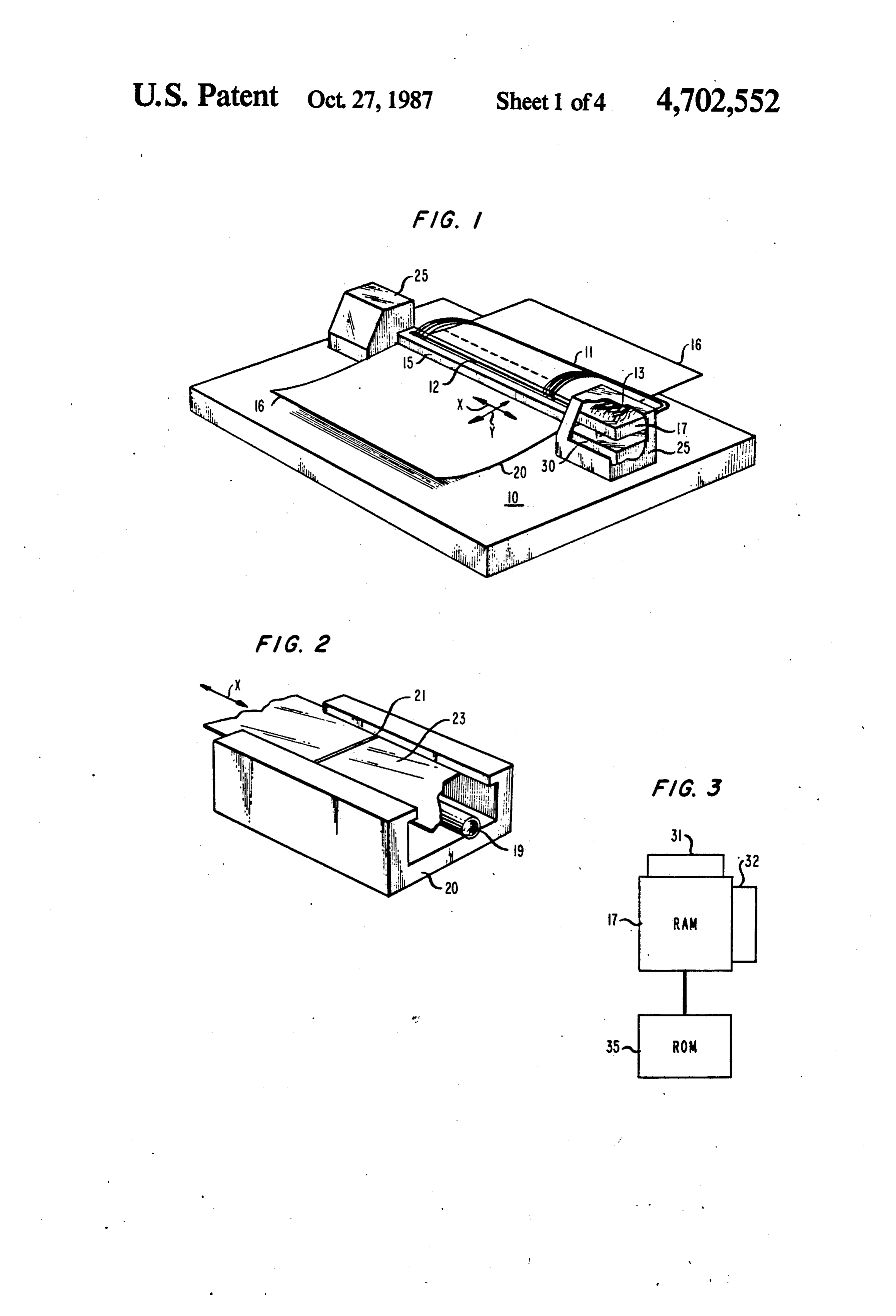
linear segment with a depth of grey scale determined by such an arrangement is not necessary for an understand the number of bit maps generated and the exposure time ing of this invention. All that is necessary is that a slit be for the cells defined by those bit maps. The term "expo passed along the fiber ends at 12 to illuminate the fibers sure time' refers to the time between the commence in sequence to establish an appropriate Look-up Table ment of a given linear scan period and the interrogation 5 or Bit Map during an initialization procedure. A suitable of the cells defined by a particular bit map. control circuit for controlling the movement of slit 21 BRIEF DESCRIPTION OF THE DRAWINGS and for controlling source 19 is represented by circuit board 30 of FIG. 1. The apparatus to accomplish initial
FIGS. 1, 3, and 4 are schematic representations of ization can be included as part of the apparatus of FIG. portions of a system in accordance with this invention. O 1, or may be a separate dedicated fixture as shown in FIG. 2 is a schematic representation of a portion of an FG, 2.
initializing apparatus for the system of FIG. 1 in accor RAM 17 includes X and Y address decoders 31 and dance with this invention. 32 in a familiar manner as indicated in FIG. 3. All bit FIGS. 5, 7, and 8 are schematic representations of locations in the RAM are initialized or precharged prior random distribution of light signals in a non-coherent 15 to each "interrogation' cycle, in which all bits are inter fiber bundle; and rogated to determine which addresses were illuminated FIGS. 6 and 9 are block diagrams of the electronic when light enters the next consecutive fiber during the organization of the system of FIG. 1. initialization process. Specifically, incident light dis DETALED DESCRIPTION charges the bit location (or locations) of the RAM cor 20 responding to the fiber at end 12 which is illuminated
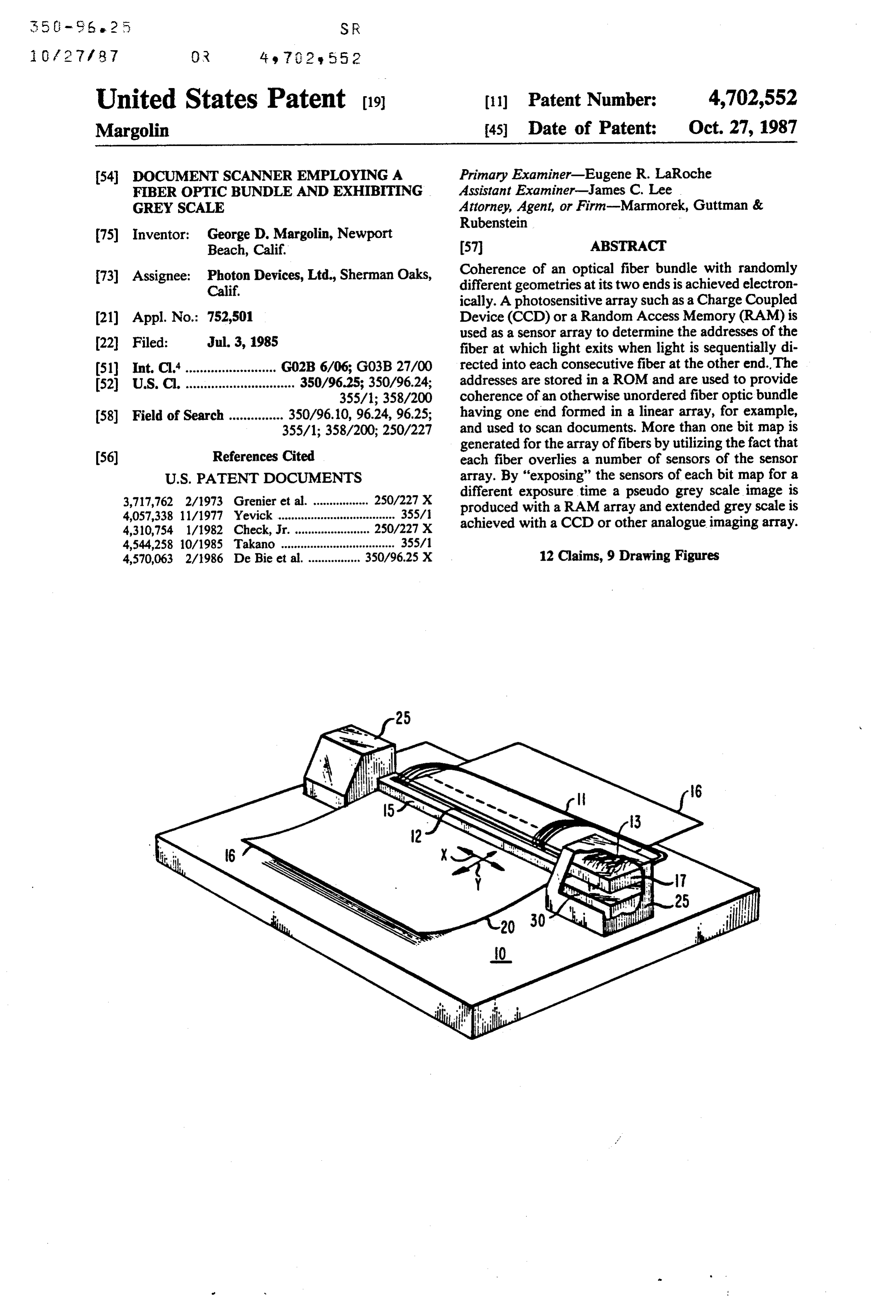
FIG. 1 shows an illustrative portable graphics input during the initialization process. The RAM is then inter device 10 in accordance with one aspect of this inven rogated and the address (or addresses) of the discharged tion. The device comprises an optical fiber bundle 11 bit location (or locations) is (are) stored in the Look-up having first and second ends 12 and 13 respectively. Table or Read Only memory (ROM) 35 under the con The ends of the fibers at 12 are constrained, conve 25 trol of control circuit 30 of FIG. 1. At the termination niently by ferrule 15 into a linear array positioned for of the initialization process, the addresses of consecu scanning successive linear segments or lines of an image tively discharged bit locations of RAM 17, correspond when moved with respect to a document 16, for exam ing to consecutive illuminated fibers, are stored. This ple, along an axis aligned with doubleheaded arrow Y. establishes the coherence between the randomly gath The ends of the fibers at 13 are not organized, but 30 ered fiber ends at 13 and the linear arrangement of fiber rather are gathered and bunched randomly, and conve ends at 12. The system is now ready for operation. niently fused. The fused bundle is abutted physically or As noted, each fiber is larger in diameter than the focused optically in a first embodiment, onto the surface area occupied by a group of bit locations in RAM. This of Random Access Memory (RAM) 17. The diameter was done, as disclosed in the above-mentioned copend of each fiber is chosen to be large compared to the area 35 ing application to ensure that at least one unambiguous of a bit location in the RAM, so that as many as twenty bit location in the sensor RAM would be illuminated (if or so bits of the RAM may correspond to each fiber at its corresponding fiber end is illuminated) during each end 13. The choice of size ensures that any light enter interrogation cycle, and so that a defect in the RAM ing a fiber at end 12 impinges a plurality of bit locations would not cause loss of information. In accordance with of the RAM when it exits at end 13. The choice also the present invention, the redundancy of about 10 to 20 ensures that a number of cells exists which is sufficient bit locations, corresponding to a single fiber, further to permit a number of bit maps to be defined. could permit as many as 10 to 20 bit maps to be made, Coherence, that is, the ordered relationship, between each including a bit location (cell) of RAM (or CCD) the light signals entering the linear array offibers at end associated which each fiber of the array. 12 and light exiting the fibers at the bundled end 13 is 45 A suitable sensor RAM is available commercially ensured by storing, in a Look-up Table in a computer, from Micron Technology Inc., of Boise, Id. The RAM or in a Programmable Read Only Memory (PROM), is divided into two sections, each 256 by 128 cells. Ac the address of a bit location in RAM 17 which senses cordingly, it is convenient in the illustrative embodi light exiting a particular fiber at end 13 as light is di ment to divide the fibers at end 13 into two arrays to rected into each of the fibers at end 12 in sequence. 50 associate with the two sections of the RAM if the Mi Apparatus, including a light source 19 enclosed by cron Technologies RAM is used. For speed of opera housing 20, is shown in FIG. 2. A side of housing 20, is tion, it may be desirable to divide the fibers into a placed adjacent to ends 12 during an initialization pro greater number of arrays to reduce the addressing re cess. That side includes a slit 12 which, for example, quirements.
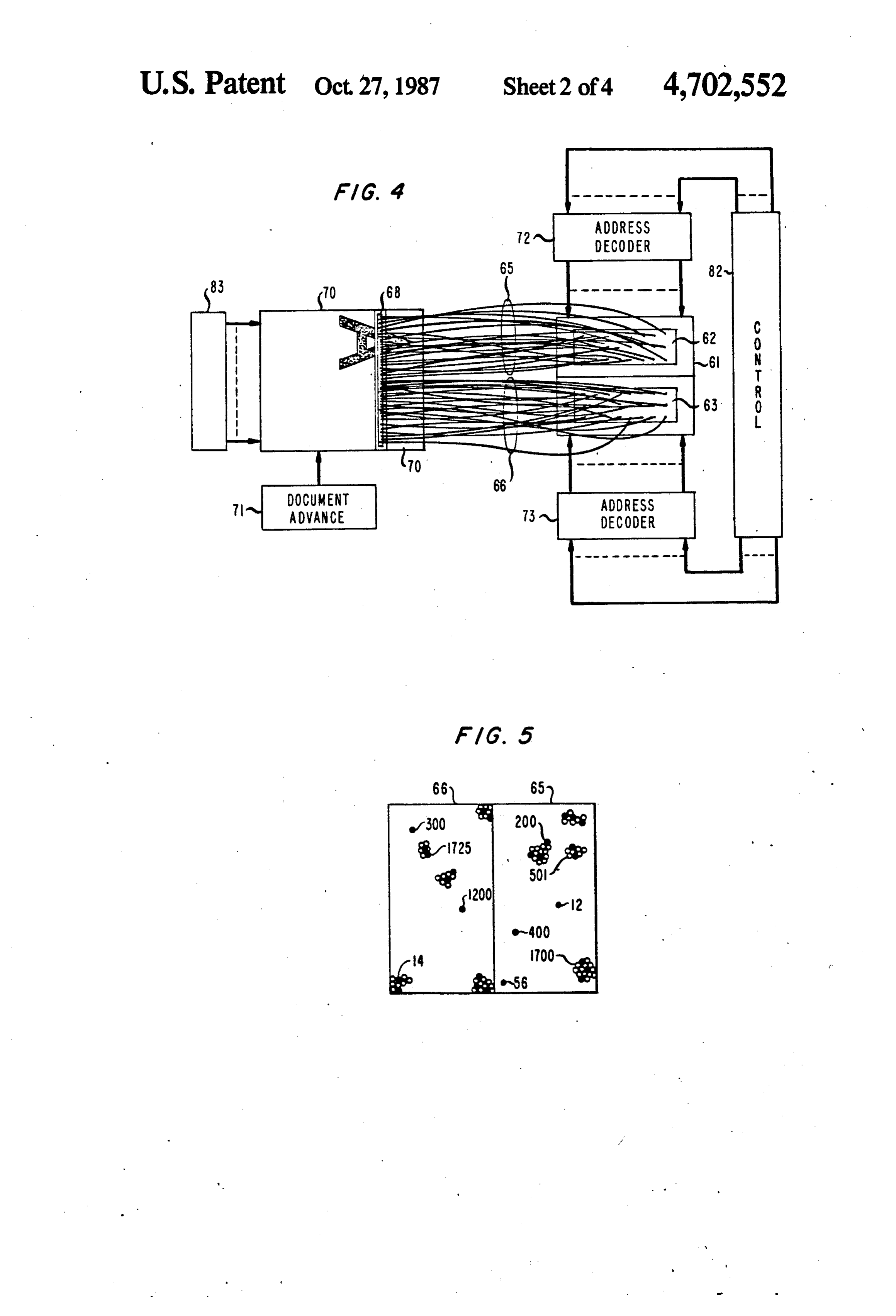
may be formed in an opaque film or tape 23 which is 55 A complete system for entering graphics information moved along an axis, represented by double headed into a computer is disclosed in detail in the September arrow X in FIGS. 1 and 2, in a manner to expose the 1983 issue of Byte Magazine, and the computer inter fibers of the linear array at end 12, in sequence, to light. faces and control software for the system are provided This causes the illumination for a sequence of bit loca in the October issue of that same publication. tions or cells in RAM 17, corresponding to the sequence 60 FIG. 4 shows schematically an arrangement of the of fibers illuminated in the linear array. The very nar type shown in FIGS. 1 and 3 for use with the system of row (less than a fiber diameter) slit 21 is progressively the above-mentioned publications. The arrangement moved along the linear array in synchronism with the includes RAM chip 61 divided into two sections 62 and interrogation of the RAM 17 so that addresses of the 63 as is available commercially. Sections 62 and 63 are RAM cells illuminated in each instance, are read out mated with randomly-bundled fiber arrays 65 and 66 and recorded. The arrangement for moving slit 21 as respectively. The other ends of the fibers are con required may be any convenient translation mechanism strained to a linear geometry by ferule 68 and positioned suitable for this purpose, and a detailed discussion of to scan a portion of a document, shown by way of illus
Page 8
tration as the letter A on document 70. A means for intensities are superimposed, a composite "pseudo' advancing document 70 is represented by block 71 and grey scale image of high resolution results. may comprise, for example, a mechanism like that used in the Houston Instruments DMP-4 plotter. Houston Look-up Table Fragment Diagram Instruments is a division of Bausch & Lomb. RAM 61 is
Output Array Associated Associated addressed by address decoders 72 and 73 under the Associated RAM RAM control of a Look-up Table implemented as part of a Input Array RAM Addresses Addresses Addresses computer or by a familiar PROM providing a bit map. Fibers 1st Bit Map 2nd Bit Map 3rd Bit Map The addressing control arrangement is represented by 507 422 424 126 block 82. O 508 73 75 77 The linear array in FIG. 4 is shown intersecting a 509
letter A on document 70. In the absence of a Look-up 51 2S40 2S42 2544 Table or Bit Map, noncoherence between the input and 52 989 99. 993 output array produces a random distribution of the light signals input to the linear array of fibers. That distribu 15 tion is shown as it appears from the output as repre The input fiber numbers shown above, constitue, sented in FIG. 5. FIG. 5 specifically, represents the illustratively, a fragment taken from the 0-3025 fibers random distribution by numbers of associated fibers in The and show three related RAM address for each fiber. the linear array placed with respect to possible positions RAM addresses are chosen from the 10 or 20 ad of the associated other ends of those fibers in arrays 65 20 dresses corresponding to a given fiber in such a way and 66. It is clear that the interrogation of RAM sec that the chosen address for each fiber in a bit map is tions 62 and 63 could make no sense of the input signals many cells away from the RAM address of nearby in the absence of a Look-up Table. fibers and the addresses for the same fiber in different bit But a Look-up Table or Bit Map which stores the maps are, arbitrarily, two addresses apart. relationship between the input of fibers 1,2,3,-and the 25 The operation of a scanner embodying the principles addresses of bit locations in RAM 61 associated with of this invention can be understood by proceeding as the output ends of those fibers, enables sense to be made follows: First the linear end of the fiber bundle is juxta of the random distribution by controlling the RAM posed with a first line of a document to be scanned. A address decoders to take the output sensed at the stored light source illuminates the document (possibly by addresses in a sequential relationship identical to that in 30 being strobed), and the storage means for storing the the linear array. Further, each of a number of bit maps, Look-up Tables or Bit Maps is activated for applying each storing that relationship, also enables sense to be the sequence of stored addresses to the RAM in order to made of the random distribution. Consequently, during provide several readings of the incoming light signals a scan period when light directs signals into the fibers at (presence or absence of light) in each of the sequence of 68, in FIG. 4, from a linear segment of the document, 35 fibers corresponding to the set of RAM addresses inter each of the Look-up Tables or Bit Maps, included in rogated according to each of the bit maps. Since the control circuit of FIG. 4, applies a set of addresses to generated sequence of RAM addresses corresponds to interrogate the memory, in order to generate output the sequence of fibers in the linear end of the bundle, in signals coherent with the fiber positions at 68. But, in each instance, the light signal outputs are coherent for accordance with the present invention, the cells of dif the cells of each bit map. These output signals are stored ferent bit maps are interrogated at different times after in memory, or transmitted, or both, in a manner entirely the commencement of a linear scan period. Next, docu consistent with the teachings of the above mentioned ment 70 is advanced incrementally with respect to fer Byte Magazine articles.
rule 68, and RAM 61 is interrogated again in accor We have now described the general organization and dance with the plurality of Look-up Tables or Bit Maps. 45 operation of a scanner utilizing a randomly organized The process is repeated until the document is entirely fiberbundle along with an electronic means for achiev scanned. The apparatus of FIG. 1 includes a lamp (not ing coherence with more than one associated bit map. shown) for illuminating the document. Provision for Now we will describe the electronic organization of the illumination may correspond to that provided in any Scale.
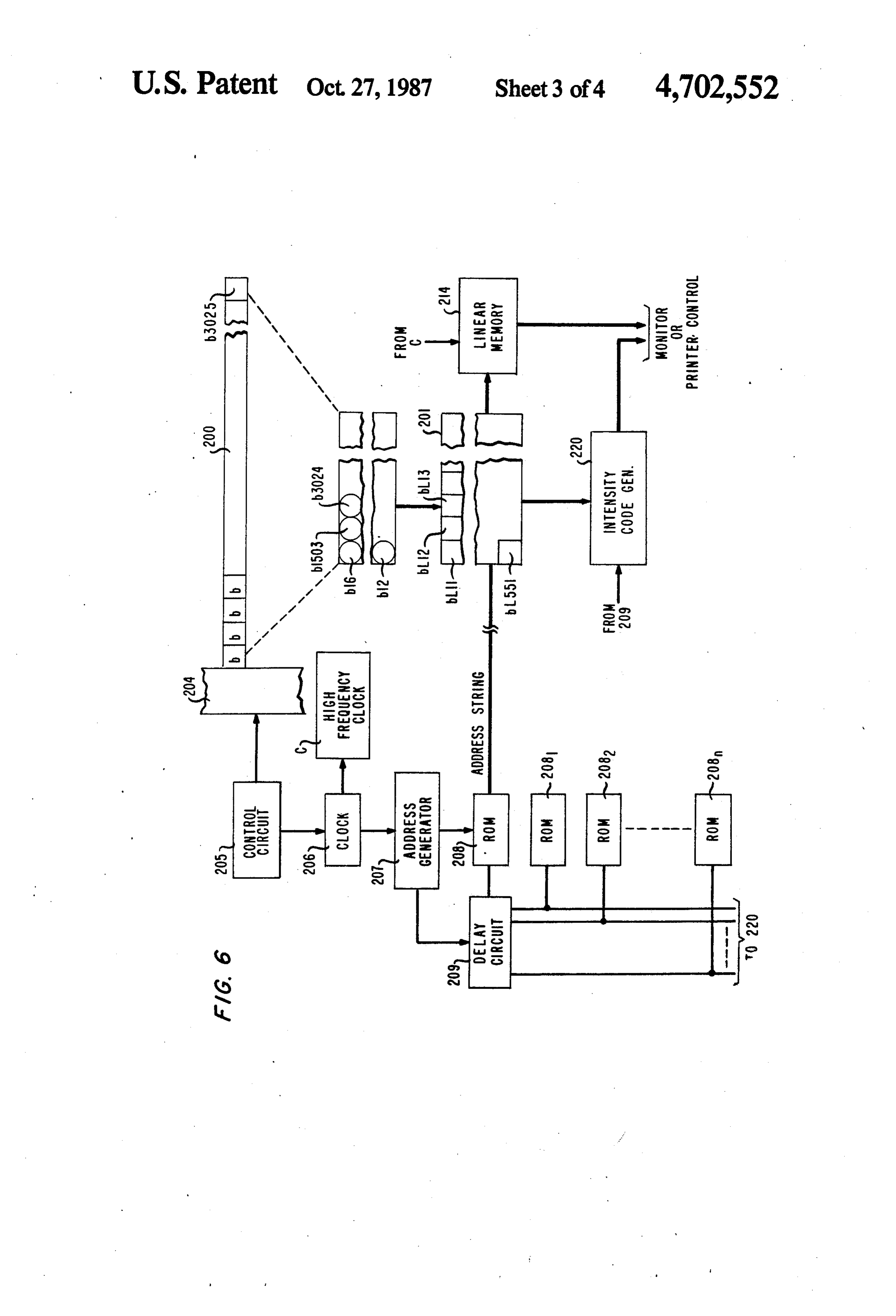
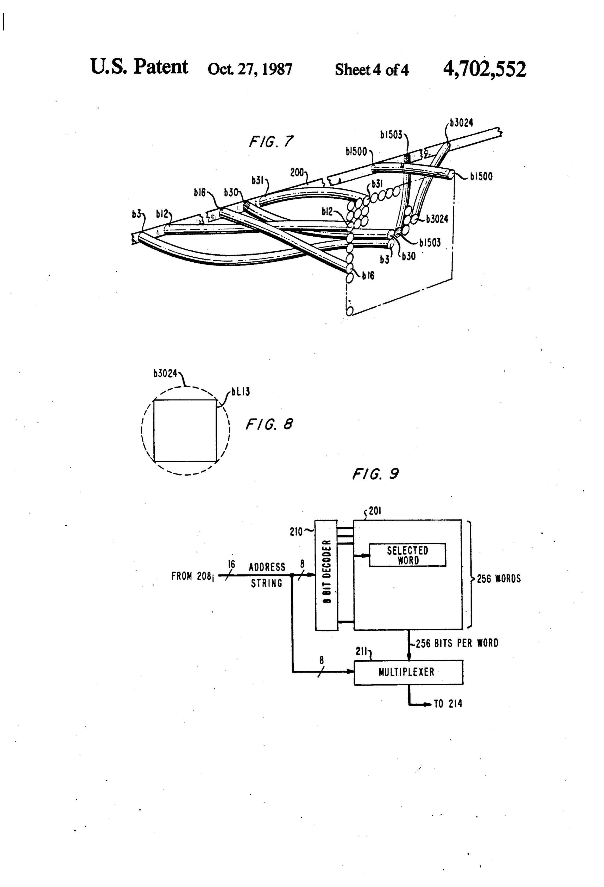
familiar copier. The illumination means is represented 50 FIG. 6 is schematic block diagram of the organization by block 83 in FIG. 4. of the scanner of FIG. 1. Rectangle 200 represents a The following Table represents first, second and linear segment (line) of a document illustratively 8.5 third Look-up Table or Bit map fragments for an illus inches long and one fiber wide. The blocks within the trative six fibers. It should be clear that the operation of linear segment are numbered from left to right as the RAM interrogation according to each Look-up 55 viewed in b1, b2, b3,-b3025. The light pattern entering Table during each scan period is entirely consistent from the linear segment of the document is, of course, with the operation described in the above mentioned scrambled when it exits the other end of the fiber. FIG. publications. The results, however, are considerably 7 represents such a scrambling. In the figure, represen different, because the optical input received by the tative fibers along the linear segment are shaded, b30, RAM during each interrogation is effectively a ran 60 and b1503, and others, b3, b12, b16, b31, b1500 and domly dissected linear input distributed over the EN b3024 are shown unshaded to represent dark and light TIRERAM-instead of a line from the array being laid areas along the linear segment respectively. The remote out on a line of the sensor, as it would be in the case of (bundled) end of the fibers is designated to correspond. a direct lens projected image. It is clear that resolution The lack of coherence is clear. is significantly improved. It is also clear that the optical 65 The bundled end of the fibers is attached (in one input, during each interrogation, from the subset of embodiment) to the face of random access memory locations corresponding to each bit map, are identical RAM 201 in FIG. 6. RAM 201 is organized illustra except for intensity. When these "images' of different tively, into fifty five rows of fifty five blocks of bit
Page 9
locations which, when multiplied out yields 3025, the several strings of addresses being applied within a cou number of fibers chosen in FIG. 6. Consequently, each ple of milliseconds dwell time to scan each linear seg fiber in the bundle corresponds In position to one of the ment. Electronics operative in the tens of nanosecond blocks of bit locations in RAM 201. FIG. 8 shows a range permit such operation.
representative fiber b3024 superimposed on a represen 5 Linear memory 214 is capable of storing 55x55 bits tative block designated bl13 for the first row in the third for each bit map. The combined stored data provides column. 55x55 grey scale code words. The memory can be The linear end of the fibers is moved, with respect to implemented, for example, by N 3025 bit shift registers a document, as indicated in FIG. 1 by a suitable me for N level grey scale or N bit maps. The shift registers chanical arrangement represented by block 204 in FIG. O are connected serially. After each scan of a linear seg 6. One suitable mechanical arrangement is shown in the ment of a document, the shift registers contain N line above-mentioned U.S. Pat. No. 4,332,458. The mechani images. The first 3025 read operations of RAM 201 (the cal arrangement is operated under the control of a con first bit map) operate to shift the registers 3025 times trol circuit 205 which is clocked by clock source 206 of yielding 3025 N bit grey scale words corresponding to FIG. 6. 15 the last scanned segment, each time a new segment is Clock source 206 also enables the generation of a scanned.
plurality of strings of RAM addresses each correspond Note that the 3025 fibers cover virtually the entire ing to the sequence b1, b2, b3. ... b3025 of the linear RAM. Thus, the 64kbits of the RAM are organized into array end of the fibers. To this end, the scanner of FIG. 3025 blocks as already indicated. Consequently, each 6 includes an address generator 207 for producing a 20 fiber corresponds to a plurality of bit locations as stated sequence of consecutive addresses. The output of ad hereinbefore. It is convenient to take the address of the dress generator 207 is connected to a plurality of read center bit location of the block in each instance rather only memories (ROMs) 2081 (2081, 2082, ... 208N) via than having to interrogate all the bit locations. (The a delay circuit 209. Delay circuit 209 may be imple center bit location will also generally be fully illumi mented by a five stage ring oscillator and a logic circuit 25 which provides the inputs to the ROMs and the RAM. nated when the corresponding fiber is illuminated, un The output of each stage of the oscillator is associated covered.edge like the bit locations which may be only partially
Thus illumination of the center bit is more with a different ROM with the remaining stage output reliably correlated with illumination of the fiber.) If we used as a toggle. The logic circuit activates the ROMs in the sequence, say, 4-3-2-1 and then 1,3,2,4 providing 30 use a sixteen bit address from generator 207 of FIG. 6, eight bits of the address select the row of the RAM and the requisite delay.
The outputs of delay circuit 209 are operative to eight bits select the column. But we can take six bits to interrogate the ROM's in sequence so that each gener select a block in a row and six bits to select a block in a ates an appropriate string of RAM addresses. An output column, leaving two bits in each instance. The remain from clock 206 is connected to address generator 207 35 ing two bits determine the offset from the corner of the selected block to the approximate center of that block.
and is operative to initiate the timed sequence of interro In this manner, the address of the center of a block is gations. Each clock pulse also is operative to activate control circuit 205 to move the linear array to a next identified with relatively few address bits. Similarly, the scan position and simultaneously to initialize address sented addresses in a plurality of address strings can be repre generator 207. Each clock pulse thus causes the address in terms of such an offset. generator to scan through the 3025 bit map addresses Operation of the system of FIG. 1 produces, say four stored in each ROM. bit maps stored in memory. Each bit map contains the Each ROM responds, in a well understood manner, addresses of a subset of cells (bit locations) of the sensor to generate an address string corresponding to the se array which correspond to all of the fibers at the bun quence of fibers at the linear array end as stored during. 45 dled end. The cells associated with each bit map sense initialization. The address string is applied to RAM 201 radiation exiting all the fibers at the bundled end. Con by means of an eight bit decoder 210, as shown in FIG. sequently, when the addresses of a particular bit map 9. The decoder is operative, in the usual manner, to are selected, a complete representation of the signals select a particular word in RAM201. Each time a clock from the fibers at the bundled end is generated. Thus, pulse occurs, the linear end of the array scans a next 50 when the addresses of the four bit maps are selected in linear segment of the document and ROM's 208; apply sequence, four representations of the signals are gener sequences of address strings to decoder 210. Each ad ated. Since the addresses of the four bit maps are read dress of each address string selects a word in RAM 201 out at four different exposure times, the representations and applies the 256 bits of the selected word to multi also comprise four different integrated light intensities. plexer (MUX) 211. MUX 211 is a 256 to 1 MUX and is 55 That is to say, a memory is provided to store the four operative to apply a binary 1 or 0 to linear memory 214 representations as "images' of the signals. Those images of FIG. 6 depending upon whether the selected block of are stored along with four codes which represent the bit addresses (i.e., b. 13 of FIG. 8) was illuminated or four different intensities to which the images corre not in the instant scan period. Linear memory 214 also spond. The intensity codes are stored in intensity code receives relatively high frequency clock pulses via generator 220 of FIG. 6. The outputs of the code gener clock C activated by clock 206 for incrementing to a ator serve to control the grey scale of the output image next of fifty five positions, each for storing fifty five bits associated with the linear memory outputs from bit (1 or 0) representing the presence and absence of light locations designated by each bit map. incident upon the consecutive blocks (b. 13 of FIG. 8) Those images are superimposed when the signals are addressed by the address string during each scan period. represented visually, either during display (on a moni Since several address strings are applied during the scan tor) or printing so that the composite image generated, of each linear segment, this procedure repeats to gener exhibits grey scale values. This can be true when the ate several representations of each linear segment, the images are transmitted to a remote facsimile device also.
Page 10
Of course, once graphics information is stored in a of fibers each as described above and each associated computer (most personal computers with graphics ca with a different RAM. Each row would then have a pability should be adequate here), that information can fiber associated with each pixel but at a different expo be manipulated to provide editing prior to printing. This sure time. The light signal sensed at the exit end of each can be accomplished through already available graphics of the fibers can then be combined in any elected logical software. The size of the document also can be reduced manner to provide a representation of the light intensity (or enlarged), providing a capability similar to micro of the image value for the associated pixel. The three film. rows even can be taken to represent red, green and blue In addition, a scanner employing a fiber bundle in for color applications. In an embodiment of this type, accordance with the principles of this invention can be 10 three rows of fibers such as that row constrained by quite small and thus portable. The entire scanner can be ferule 68 of FIG. 4 are abutted against one another configured like a wand so that, together with a feed across page 70. The other ends of the fibers are associ sensing mechanism and light source, an assembly ap ated proximately inch by 3 inches by 9 to 10 inches may that aswith RAM chips such as 61 of FIG. 4. It is clear page 70 is incremented, the corresponding fibers form an entire copier, for graphic input or Optical of consecutive
rows becomes aligned with a particular
Character Recognition (OCR) applications. pixel in three consecutive time periods so that the out The invention has been described in terms of a RAM which is inherently binary. As has been mentioned here puts of the three fibers represent the light at that pixel. Also, the fibers of the three rows above can actually inbefore, inherently analogue devices such as CCD's can be used instead. In such cases, the use of redun 20 be located in the same row interleaved in three sets, 1,2,3,1,2,3 ..., for example. But still all the first fibers are dancy due to the correspondence of many CCD cells to bundled at the exit end and associated with a first sensor a single fiber permits an extensive of grey scale over and (RAM or CCD) array whereas all the second fibers and above what could be achieved with a CCD array alone, all the third fibers are associated with the second and for example.
Grey scale capabilities of CCD's, for example, are 25 thirdthis sensor arrays respectively. Timing is simplified in embodiment over the three row embodiment. The limited. This limitation is due to the familiar dark cur three fibers rents which characterize such devices particularly at within the chosen pixel(1,2 and 3) for any pixel, of course, must fit room temperatures. Because of these dark currents, size. CCD's are rated at about eight bits of grey scale. At achieving As mentioned hereinbefore, other techniques aid in cryogenic temperatures, twelve bits of grey scale or 30 can be capitalized grey scale. The RAM cell sensitivity spread better can often be achieved. upon, for example, by initializing For high density films such as those used with x-ray more than once at different light intensities and storing recording, more than eight bits of grey scale would be the addresses of sets of cells with different light sensitiv required for an array of CCD's utilized to digitize the ities. The natural spread in sensitivities provides a built film's image in a manner to do full justice to the film's 35 in grey scale capability. Also, not all the cells associated capabilities. The technique herein disclosed permits, for with a single fiber may be illuminated at some low light example a modest eight bits of grey scale, but permits intensity while all are at high intensities. The averaging the eight bits to be achieved at each of a group of differ of the outputs of the cells may provide further grey ent exposure times. Although, overlap may occur, if scale capabilities.
closely timed exposures are chosen, an extended grey 40 What is claimed is:
scale (ten bits deep or more) is achieved by overlaying 1. In combination, a fiber optic bundle having first or superimposing different times for each exposure. For and second ends arrayed randomly in first and second example, for a two millisecond overall exposure time geometries respectively, means for directing input radi period, one half milliseconds between four separate ation signals representative of data at the fibers of said "exposures' controlled by four bit maps as in FIG. 6 45 first end, utilization means cooperative with said fibers provides a grey scale of eight bits for high exposure and at said second end, and electronic control means for a grey scale of eight bits for each of the other exposures, associating the signals exiting from said second end with thereby extending the total range captured. This can the corresponding input signals at said first end in a provide ten bits without the size and expense of more manner to preserve coherence therebetween, said elec costly sensors or cryogenic apparatus. 50 tronic control means being adapted to provide redun A further advantage of the "staggered exposure” dant sensor means in N subsets each having at least one array disclosed herein is that the problem of CCD sensor for each of said fibers, said electronic control "blooming' effects are mitigated if not eliminated alto means comprising means for activating said N subsets gether. The reason for this is that blooming is caused by for N different time periods in a manner to generate N charge spill over from a saturated cell to next adjacent 55 like representations of said input signals, and means for cells thus causing loss of detail. But, adjacent cells are associating said N like representations with N different not read out together in accordance with the present radiation intensities corresponding to said N different invention. Instead, spaced apart cells are read out - cells time periods.
too far apart to be affected by blooming. Consequently, 2. A combination in accordance with claim 1 includ even inherently analogue devices capable of providing ing means for constraining the fibers of said first end grey scale, provide extended grey scale capabilities into a first geometry which comprises a linear array. herein. More important regarding reduction in bloom 3. A combination in accordance with claim 2 includ ing effects is the fact that those segments of the image ing means for constraining the fibers of said second end that are highly saturated (brightly lit) will be selected into a rectangular array.
from that bit map with the shortest exposure, thereby 4. A combination in accordance with claim 4 wherein greatly reducing image spillover. said electronic control means comprises memory means Of course, a scanner in accordance with the princi for associating the location of each fiber at said second ples of this invention can employ three sequential rows end with a corresponding fiber at said first end.
Page 11
5. A combination in accordance with claim 5 wherein 8. A combination in accordance with claim 7 also said control means includes a Random Access Memory including first means for moving said linear array trans (RAM), said RAM being responsive to radiation signals versely with respect to an initial linear reference posi for providing the addresses of cells at locations therein tion.
exposed to radiation sequentially, and said control 9. A combination in accordance with claim 8 wherein means comprises means for generating said addresses said first means comprises means for moving said linear sequentially in response to a first signal. array incrementally with respect to a sheet of paper on 6. A combination in accordance with claim 5 also which said initial linear reference position is defined. including means juxtaposed with the fibers of said first 10. A combination in accordance with claim 9 also end for moving a document with respect to those fibers O including means for applying to said storage means said in response to said first signal, and radiation means for sequence of addresses in subsets between consecutive exposing at least a linear segment of said document for ones of said incremental movements of said linear array, generating said first signals. storage means responsive to said addresses for storing 7. A combination of elements comprising a fiber optic signals representative of the presence or absence of array having first and second ends, means for constrain 15 radiation in the associated fiber at said addresses in ing the first ends of said fibers into at least one linear subsets, and means for providing a coded indication of array in a manner to permit exposure of said fibers to the light intensity associated with outputs from said electromagnetic radiation, at least a first radiation sens storage means associated with each of said subsets. ing means comprising a plurality of sensing elements 11. A combination of elements in accordance with having discrete addresses and organized in an array 20 claim 10 wherein said means for constraining constrains having a surface with a first area, said second ends of said first ends of said fibers into first, second and third said fibers being bundled randomly into an area less rows, said combination also including first second and than or equal to said first area and associated with said third sensing means associated with the second ends of surface, storage means for storing the addresses of said said rows of fibers respectively. sensing elements in N subsets each including sensing 25 12. A combination of elements in accordance with elements which correspond to the positions of the first claim 10 said combination also including first second end of said fibers in said linear array, means for activat and third radiation sensing means, said fibers being ing said elements of said array, and means for interro organized into first second and third interleaved sets gating said elements of said N subsets at N different said sets having second ends associated with said first times in a manner to create N representations with N 30 second and third sensing means respectively. different radiation intensites
Provenance
- Collection
- Cited prior art
- Original PDF
- patentimages.storage.googleapis.com →
- Filed
- 1985-07-03
- Pages
- 11
- Method
- pdftotext (the PDF's own text layer) + pdftoppm 300dpi page scans
- Source
- Google Patents bibliographic record
- Granted
- 1987-10-27
- Inventors
- George D. Margolin; PHOTON DEVICES Ltd
- Transcribed from
- patentimages.storage.googleapis.com →