patent · US6278429
Bistable reflective cholesteric liquid crystal displays utilizing super twisted nematic driver chips
21 August 2001
Page 1 — bibliographic record
(12) United States Patent (10) Patent No.: US 6,278,429 B1 Ruth et al. (45) Date of Patent: Aug. 21, 2001
(54) BISTABLE REFLECTIVE CHOLESTERIC 97, Copyright by the Society For Information Display, LIQUID CRYSTAL DISPLAYS UTILIZING Metropolitan Detroit Chapter.
SUPER TWSTED NEMATIC DRIVER CHIPS
* cited by examiner (75) Inventors: Jonathan C. Ruth, Kent, OH (US); Primary Examiner Richard Hjerpe Richard Hewitt, Beaverton, OR (US); ASSistant Examiner-Kimnhung Nguyen
Philip J. Bos, Hudson, OH (US) (74) Attorney, Agent, or Firm-Renner, Kenner, Greive, (73) Assignee: Kent State University, Kent, OH (US) Bobak, Taylor & Weber
(*) Notice: Subject to any disclaimer, the term of this patent is extended or adjusted under 35 A driving circuit for a reflective bistable cholesteric liquid U.S.C. 154(b) by 0 days. crystal display which includes one Substrate having a plu rality of column or Segment electrodes opposed by another (21) Appl. No.: 09/151,420 Substrate having a plurality of row or common electrodes. The interSecting column and row electrodes with the cho (22) Filed: Sep. 11, 1998 lesteric material therebetween form a plurality of pixels. The (51) Int. Cl." ....................................................... G09G 3/36 driving circuit Selectively applies a Voltage to the row and (52) U.S. Cl. ............................ 345/94; 34.5/208; 34.5/210; column electrodes to control the appearance of the choles
teric material. In particular, the driving circuit includes at least one common driver coupled to respective common (58) Field of Search ................................ 345/94, 95, 208, electrodes with each common driver having a first and a 34.5/210; 349/96, 98 Second common frame Switch with corresponding high or (56) References Cited low inputs. The first and Second common frame Switches are linked to one another by a common frame line. The high and
data Switches, the first common frame Switch a first and a 5,570,216 10/1996 Lu et al. .............................. 359/101 Second common Voltage input and the Second column frame 5,748.277 * 5/1998 Huang et al. ... 34.5/210 Switch having a third and a fourth common Voltage input 5,933,203 8/1999 Wu et al. ............................... 349/35 5,942,154 * 8/1999 Kim et al. ......... 349/115 connected to each other. The driving circuit also includes at 5,995,180 * 11/1999 Moriwaki et al. ... 349/96 least one Segment driver coupled to respective Segment 6,034,752 * 3/2000 Khan et al. ....... ... 349/74 electrodes. The at least one Segment driver is configured 6,061,108 5/2000 Anderson et al. ..................... 349/98 much the same as the common driver, except that it receives
OTHER PUBLICATIONS
different input Voltages. By Selectively toggling the frame and data Switches of each driver, a dynamic drive Scheme
J. Ruth, R. Hewitt, and P. Bos, Low CoSt Dynamic Drive can be applied to the display. Scheme For Reflective Bistable Cholesteric Liquid Crystal
Displays, pp. 89-94, Sep. 22-23, 1997, Flat Panel Display 35 Claims, 7 Drawing Sheets
WnAS
Page 2
Drawing sheet — no readable text.
Page 3
COMMON HOLD/EVOLVE HOLD/EVOLVE HOLD/EVOLVE to 25 a 25 to 25 H O O O 9 -25 9-25 S-25 -5O -5O - -5O O 2 4. O 2 4. O 2 4 TME TME TME
PXEL
COMMON SELECT P}XEL SELECT NON-SELECT 5O 5O 5O up 25 up 25 to 25 - O he O H. O. 9 -25 d-25 c -25 -5 O -5o -5O O 2 4. O 2 4. O 2 4 TIME TME ME
COMMON NON-SELECT SELECT DAA NON-SELECT DATA 5O 5O 5O
S -25 S-25- 9 - 25 -5 O -5O -5O O 2 4 O 2 4. O 2 4 TME TME TIME N- —-
Page 4
Drawing sheet — no readable text.
Page 5
Drawing sheet — no readable text.
Page 6
Drawing sheet — no readable text.
Page 7
Drawing sheet — no readable text.
Page 8
Drawing sheet — no readable text.
Page 9
BISTABLE REFLECTIVE CHOLESTERC The liquid crystal material in between the interSecting LIQUID CRYSTAL DISPLAYS UTILIZING electrodes form a pixel. As shown in FIGS. 2A and 2B, the SUPER TWSTED NEMATIC DRIVER CHIPS appearance of each pixel is controlled by a pixel Voltage waveform which comprises a sequence of three RMS volt
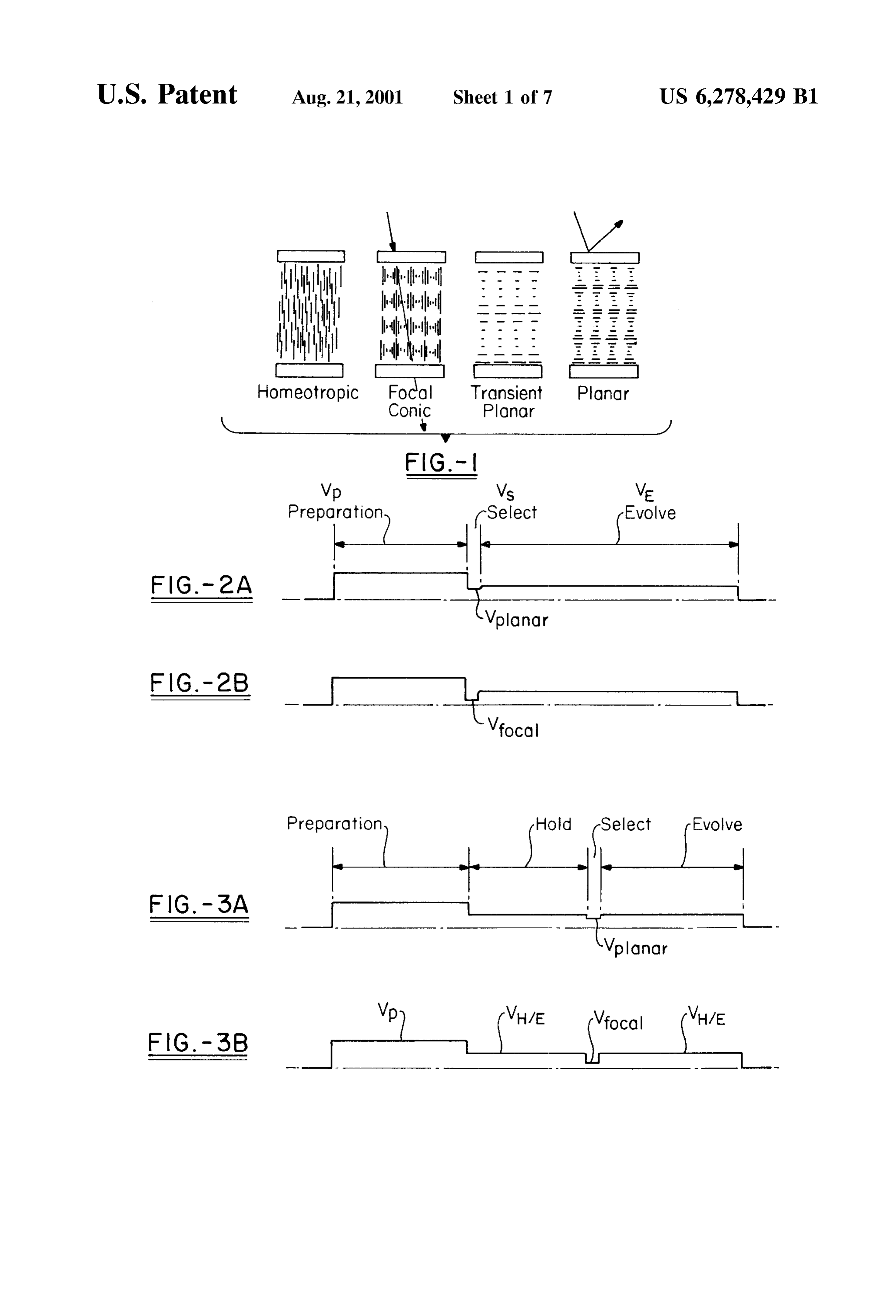
GOVERNMENT RIGHTS ages: Vpreparation Vselect/non-select and Vevolve VYpreparation O The United States Government has a paid-up license in V, drives the cholesteric liquid crystal material into the homeotropic texture regardless of its initial texture. Appli this invention and may have the right in limited circum cation of Veterset, or Vs determines if the homeo stances to require the patent owner to license others on tropic texture relaxes into the planar (V) or the focal reasonable terms as provided for by the terms of Contract conic texture (V). The evolution Voltage or V. No. N61331-94K-0042, awarded by the Defense Advanced Serves two functions. First, it permits the focal conic texture Research Projects Agency. to evolve from the transient planar texture that results from TECHNICAL FIELD applying V. The evolution Voltage also restores and maintains the homeotropic texture after V is applied
This invention relates to the operation of liquid crystal 15 allowing relaxation to the planar texture which occurs when displayS. In particular, the present invention relates to a V is removed. It has been determined that display driving circuit for operating a cholesteric liquid crystal update Speed can be increased by applying the Voltages display. Specifically, the present invention relates to a driv Vpreparation and V across many rows simultaneously. ing circuit employing Specially modified drivers that are Once V is removed from the last addressed row, all normally used in Super twisted nematic liquid crystal dis power is removed from the display and the desired indicia playS. appears on the display.
BACKGROUND ART Implementation of Such a drive Scheme has proven to be quite costly. In particular, previous displays required
Cholesteric liquid crystal materials are known and dis 50-60V (RMS) to drive the cholesteric liquid crystal mate closed in U.S. Pat. Nos. 5,437,811; 5,695,682; 5.453,863; 25 rial into the homeotropic texture from which it relaxes into and 5,691,795, all of which are assigned to the assignee of the reflective planar texture. Since the use of cholesteric the present invention and which are incorporated herein by liquid crystal materials in displayS is relatively new, there reference. The primary advantage of the bistable cholesteric are no commercially available electronic driving circuits liquid crystal materials disclosed in these patents is that they uniquely designed to apply the necessary Voltage waveforms can be driven to a desired texture with application of a to a display.
Voltage and remain in that texture after removal of the One option that was initially investigated was to employ applied Voltage. AS Seen in FIG. 1, bistable cholesteric liquid a multiplexed super twisted nematic (STN) display driver. crystal materials are known to exhibit at least four States or STN displays are addressed constantly So that each pixel textures: homeotropic, focal conic, transient planar, and always has an applied Voltage acroSS it that is the combi planar. Both the homeotropic and transient planar textures 35 nation of waveforms being applied to the appropriate inter are considered transitory and do not remain after removal of Secting electrodes. The “state' or texture of a particular pixel an electric field. These transitory textures are employed to (on or off, light or dark) depends on the average Voltage facilitate the transformation of the cholesteric liquid crystal acroSS the pixel during a single Scan or update of the display. material into either a weakly light Scattering, transmissive The difference between the average voltages of these two focal conic texture or a reflective planar texture. 40 pixels states is small, on the order of about 0.1 volt. This The next step in the development of bistable cholesteric difference is generated entirely by the choice of Voltage, liquid crystal devices was focused on how to drive the either high or low, applied to the pixel while it is Selected for cholesteric liquid crystal material quickly between the focal update. The number of DC voltage levels required to drive conic and planar textures. This development is necessitated a STN display is relatively small. Four voltage levels are by the desire to provide efficient operation of the device, 45 required for each common/row and Segment/column wave with as fast as possible update rates. Such driving Schemes form and typically, two of these voltage levels are common are found in U.S. Pat. No. 5,748,277, and in U.S. patent to both. Accordingly, only six distinct DC voltage levels, application Ser. No. 08/852,319, both of which are owned by which are Separate from the logic Voltage inputs, are the assignee of the present invention and which are incor required to address an STN display. STN driver chips also porated herein by reference. Initially, a three phase dynamic 50 include a data input called the frame line that Selects drive scheme, as shown in FIGS. 2A and 2B, was employed between two fixed pairs of display Voltage inputs for all the to control the appearance of the cholesteric device. AS is outputs on a chip. For example, if the display Voltage inputs discussed in the above patents, the liquid crystal material is are labeled V, V, V, and V, the frame line can Select disposed between two Substrates, one of which has a plu between either the pair V and V or the pair V and V. No rality of row electrodes and the other which has a plurality 55 other Selections are possible. Of course other label designa of column electrodes orthogonal to the row electrodes. tions could be used for the voltage inputs. Each STN driver Application of Voltage waveforms to the electrodes is mul chip also includes a shift register containing one data bit per tiplexed or applied in a predetermined Sequence. Hence, chip output. Each bit Selects one of the two display Voltage these displays are Sometimes referred to as multiplexed inputs Selected by the frame line. Accordingly, each bit can displayS. Those skilled in the art will appreciate that multi 60 Select between V and V2 or between V and V. Once again, plexed displays are not limited to "row and column elec no other Selections are possible. The Voltages applied to the trode patterns. Segmented liquid crystal displays, Such as display Voltage inputs must obey Strict rules. At a minimum, clock faces and calculator displays, may also be multi the rule (VeVeVeV) must be obeyed. Moreover, it is plexed. In either type of display the term “common elec typical to require two of the four display voltage inputs (V. trode' may be used to refer unto a row electrode, and the 65 and V) to be set very near to the chip’s upper Supply voltage term “segment electrode' may be used to refer to a column while the other two display Voltage inputs (V and V) are electrode. Set very near the chip's lower Supply Voltage. These require
Page 10
ments are intended to ensure proper chip operation and are It is a further object of the present invention to provide a primarily a function of the chip design. multiplexing drive circuit and method for use, as above, in Although it was desired to employ the STN driver chips which common and Segment drivers are coupled to corre to drive the cholesteric liquid crystal display because of their sponding common and Segment electrodes which are relatively low cost (about 2 cents per output), it was readily employed to drive the liquid crystal material disposed apparent that the drive Scheme requirements of cholesteric between a pair of Substrates.
liquid crystal displays were significantly more Severe than It is yet another object of the present invention to provide Super twisted nematic displays. The state of a STN pixel the drive circuit and method for use, as above, in which each depends only on the average Voltage across the pixel during common and Segment driver contains at least two frame a single update of the display and not on the Specific
Sequence of Voltages applied to the pixel. While cholesteric Switches, receives each of which has a high and low input which
Voltage waveforms that are transferred to a plurality liquid crystal displayS respond to the average Voltages of data Switches which in turn are coupled to respective applied to them, the State of a pixel depends on the Sequence electrodes.
of RMS/average Voltages applied during an update. AS noted previously, the dynamic address Scheme requires the proper 15 It is yet another object of the present invention to provide application of RMS voltages V, Vsfits and V in order to the drive circuit and method for use, as above, in which a select between the two stable cholesteric liquid crystal frame line is employed to toggle the frame Switches in each textures. The only known way to address cholesteric liquid of the drivers to Select a voltage input pair which can be crystal displays with the dynamic drive Scheme was to applied to the display.
employ high Voltage analog Switches to generate the nec It is still another object of the present invention to provide essary row waveforms. the drive circuit and method for use, as above, in which at A first attempt at employing STN drivers resulted in providing half of the Signals needed to drive a cholesteric least one of the frame Switches in the common and Segment liquid crystal display. In this approach, the STN driver chips driverS thereby has two of its inputs connected to one another, allowing an arbitrary waveform to be submitted to were employed to generate the column waveforms and high the corresponding electrodes. Voltage analog Switches were employed to generate the row 25 It is still a further object of the present invention to waveforms. The row waveforms were AC waveforms, and the necessary RMS voltages were generated entirely by provide the drive circuit and method for use, as above, in these row waveforms. The column waveforms supplied by which each common and Segment driver has a plurality of the Segment/column drivers were of Small amplitude and data Switches which direct one of the frame Switch outputs amounted to inconsequential noise on all rows except the to the appropriate electrodes.
row being addressed. On the row being addressed, the row It is an additional object of the present invention to waveform Voltage levels were comparable to the column which provide a driving circuit and method for use, as above, in waveform (data) Voltage levels. AS Such, the proper select Voltageone of the row frame Switches receives three different values So that the indicia appearing on the display and non-Select Voltages could be generated by changing the phase of the column waveforms. 35 appears row by row.
The fundamental characteristic of STN driver chips that provide It is still yet another object of the present invention to led to this hybrid mixture of driver chips and analog which one a driving circuit and method for use, as above, in Switches is that STN driver chips are “unipolar,” that is, the Voltage values of the row frame Switches receives two different output voltages can range, for example, from 0–40 Volts, as So that the indicia appearing on the display opposed to “bipolar wherein the output voltages would 40 appears all at once.
range from -40V to +40V. It was not thought possible to The foregoing and other objects of the present invention, generate the necessary RMS voltages given the limited which shall become apparent as the detailed description voltage range of STN drivers, typically no more than 40 proceeds, are achieved by a bistable cholesteric liquid crys volts, versus the 200 volts required for the analog switches tal display, comprising a pair of opposed Substrates, one used in the initial embodiment. In particular, the initial 45 Substrate having a first plurality of electrodes, the other embodiment was designed So that one high Voltage analog Substrate having a Second plurality of electrodes oriented in Switch chip was needed to drive every two rows. At eight a direction different than the first plurality of electrodes, a Switches per chip, four Separate analog Switches controlled cholesteric liquid crystal material disposed between the pair each row. Accordingly, a four inch by four inch display used of opposed Substrates and forming a pixel at each interSec in the initial embodiment had 320 rows, so 160 of the high 50 tion of the first and Second plurality of electrodes, a first Voltage analog Switch chips were required. This forced the Super twisted nematic driver having a plurality of outputs cost of the drivers alone to over S3,000.00. Although the connected to the first plurality of electrodes, and a Second drivers in association with the other circuitry were effective Super twisted nematic driver having a plurality of outputs in driving the display, it was quite cost prohibitive. connected to Second plurality of electrodes, wherein both the Moreover, Scaling up to a page-size display at a reasonable 55 driverS receive a plurality of Voltage input waveforms for resolution (133 DPI) was clearly out of the question in trodes. Selective transmission to first and Second plurality of elec attempting to develop a commercially cost-effective choles teric display. Other aspects of the present invention are attained by a
DISCLOSURE OF INVENTION
method for addressing a bistable cholesteric liquid crystal 60 display which has a pair of opposed Substrates, one of the
It is thus an object of the present invention to provide a Substrates having a first plurality of electrodes, the other low-cost dynamic drive circuit for multiplexing a bistable Substrate having a Second plurality of electrodes oriented in reflective cholesteric liquid crystal display using drivers a direction different than the first plurality of electrodes, the originally designed for Super twisted nematic displayS. Substrates having cholesteric liquid crystal material disposed It is another object of the present invention to provide a 65 therebetween to form a pixel at each intersection of the first drive circuit which employs up to 8 different voltage levels and the Second plurality of electrodes, the first plurality of which can range anywhere from 0 to 80 volts. electrodes having at least a first driver coupled thereto and
Page 11
S 6 the Second plurality of electrodes having at least a Second FIGS. 2A and 2B are exemplary dynamic drive voltage driver coupled thereto, the method comprising the Steps of Sequences for driving cholesteric liquid crystal material to applying a plurality of Voltage input waveforms to the first either a focal conic or planar texture; driver and the Second driver, wherein the Voltage input waveforms are 50 volts or less, selectively transmitting the of FIGS. 3A and 3B are four phase dynamic drive schemes the present invention;
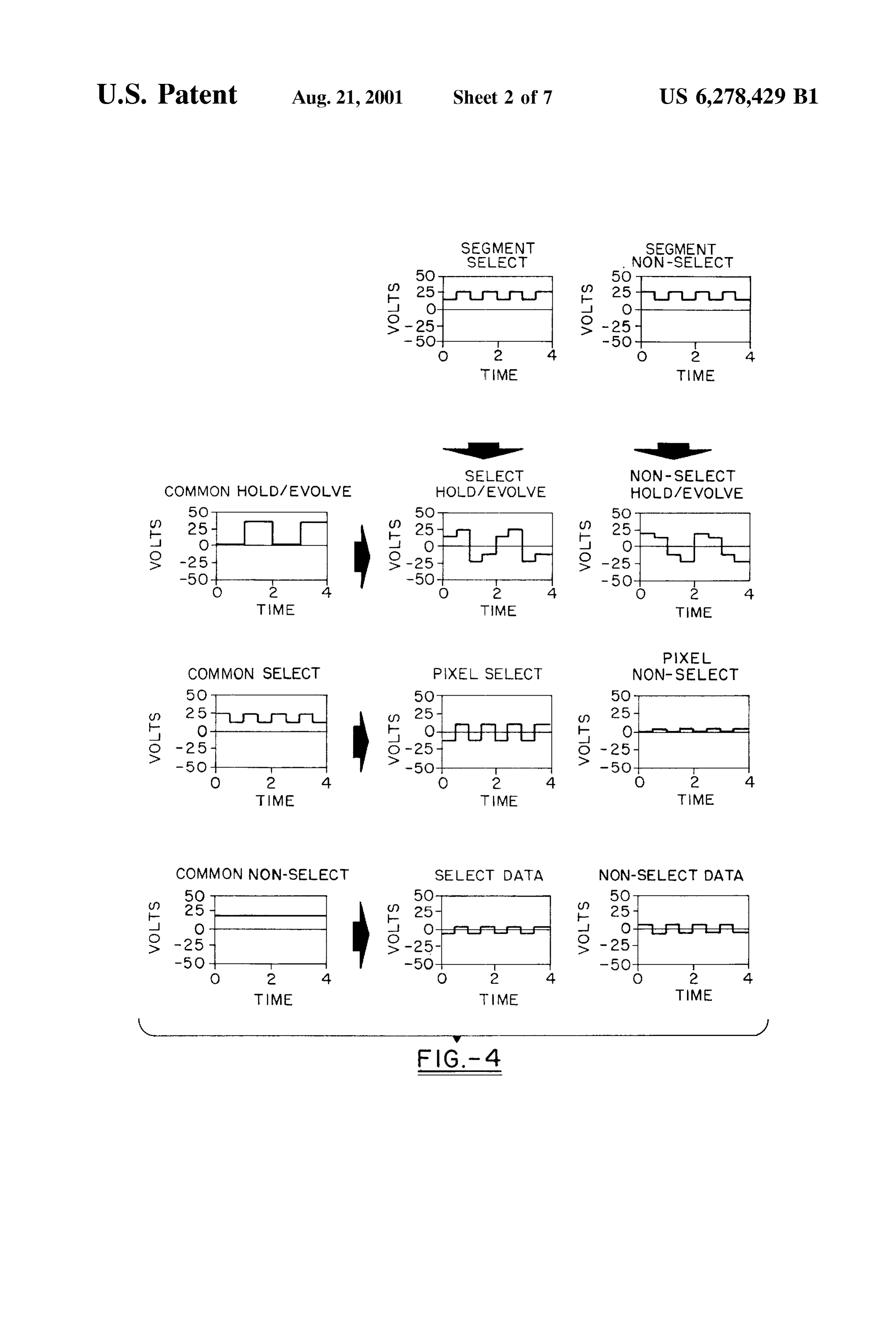
plurality of Voltage input waveforms through the first and the Second drivers to generate respective first and Second FIG. 4 illustrates the unipolar component waveforms of output waveforms, and combining the first and Second the dynamic drive Scheme that are applied in each mode of output waveforms at the interSecting electrodes to generate the present invention without showing the row and column a pixel waveform that drives the cholesteric liquid crystal preparation waveforms which are simply Square waves material to the desired appearance. running rail to rail;
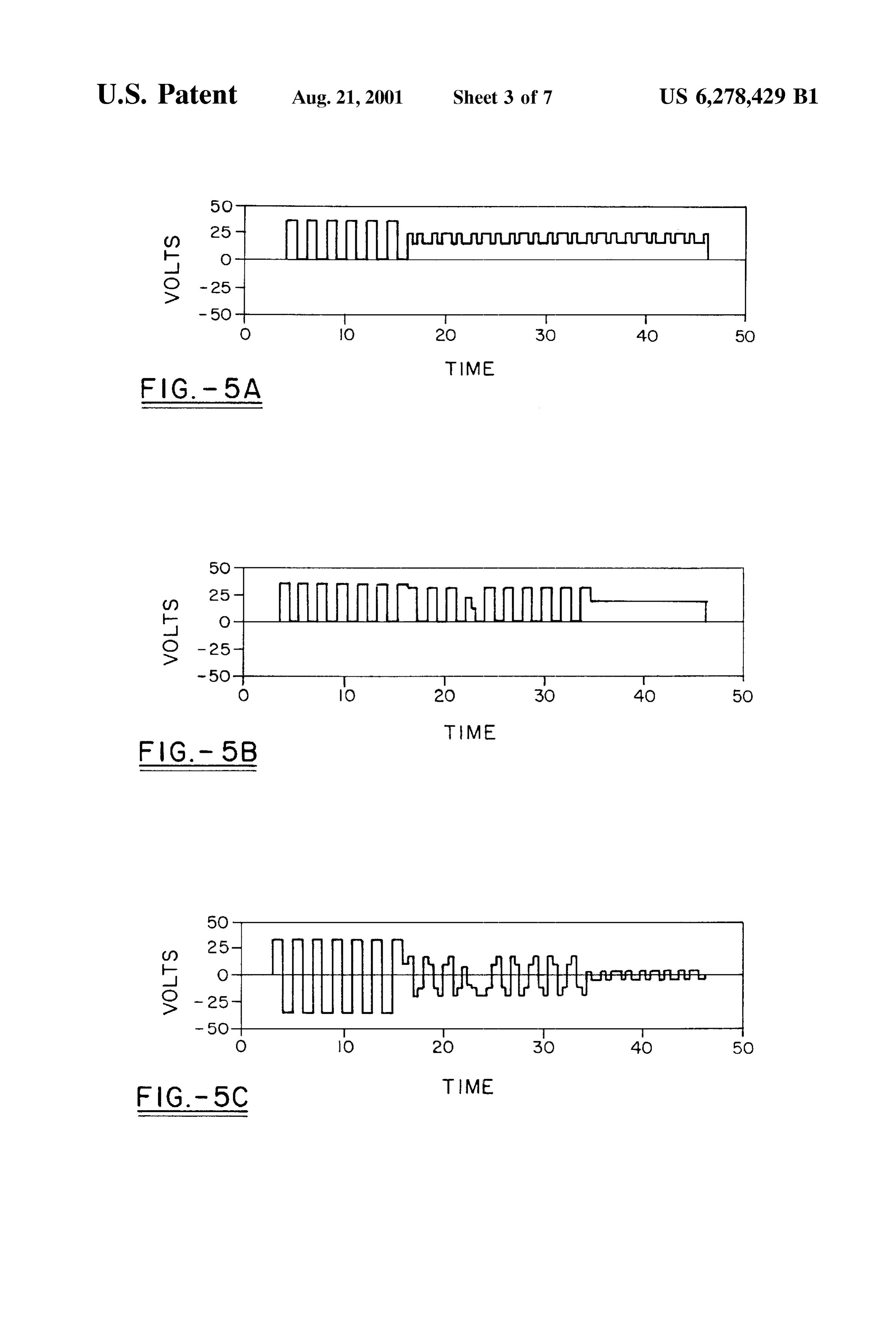
Still other aspects of the present invention are attained by FIGS. 5A-C illustrate the combination of the component a driving circuit for a reflective bistable cholesteric liquid waveforms of FIG. 4 to show the typical column, row, and crystal display which includes one Substrate having a first pixel waveforms, respectively, employed in the present plurality of electrodes opposed by another Substrate having 15 invention;
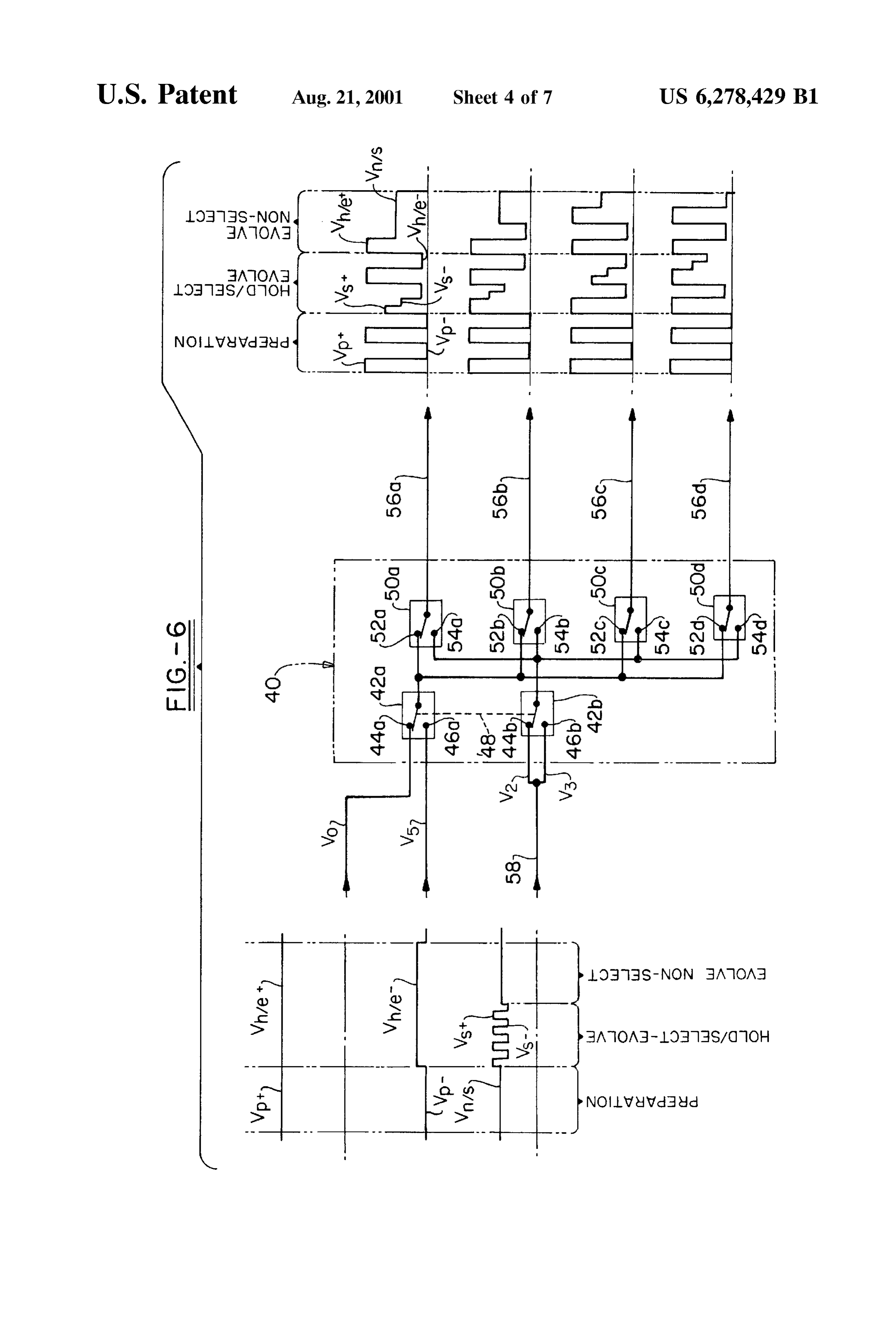
a Second plurality of electrodes, wherein the interSection of the first and the second plurality of electrodes with choles in FIG. a 6 is a block diagram for a common driver employed driving circuit of the present invention in which a Scan teric liquid crystal material disposed therebetween form a mode is employed;
plurality of pixels, the driving circuit Selectively applying
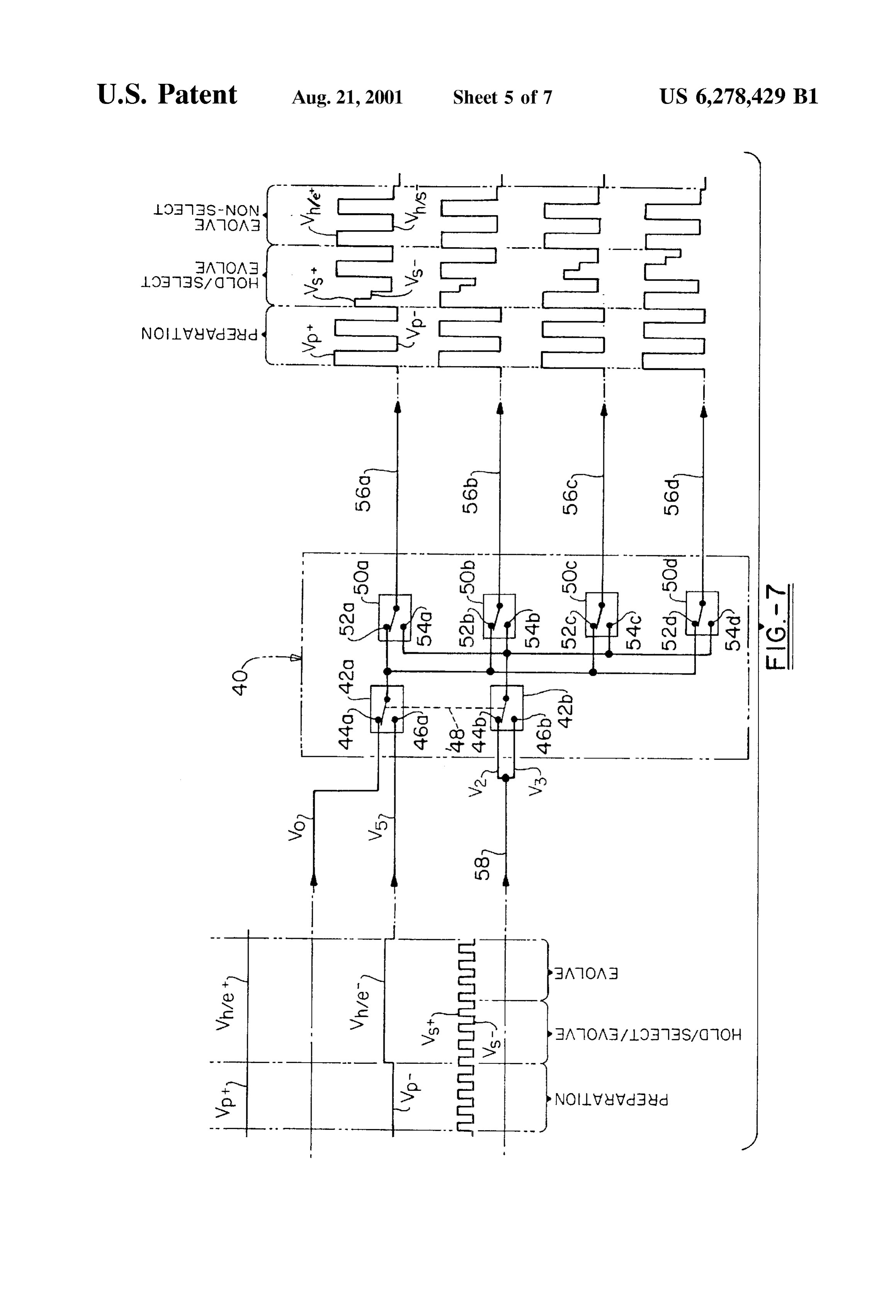
Voltages to the first and the Second plurality of electrodes to FIG. 7 is a block diagram for a common driver employed control the appearance of each pixel, the driving circuit in a driving circuit of the present invention in which a flash comprising at least one common driver coupled to the first mode is employed;
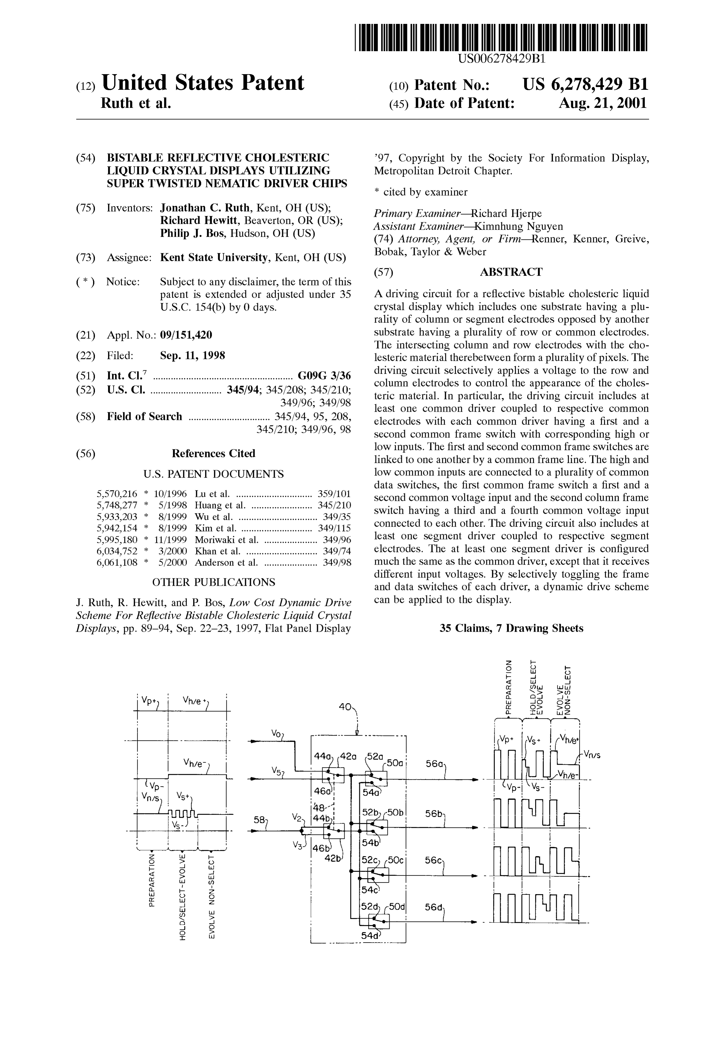
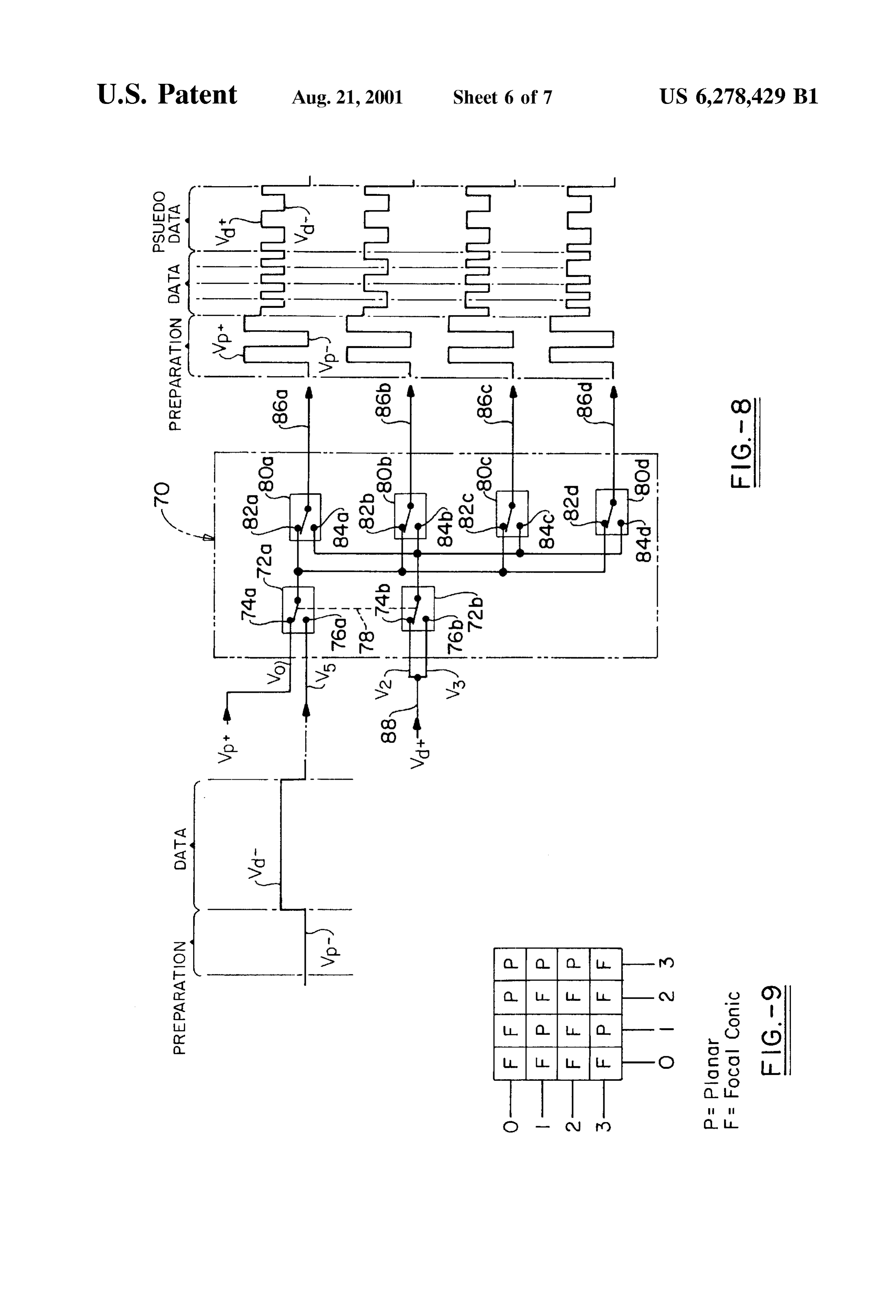
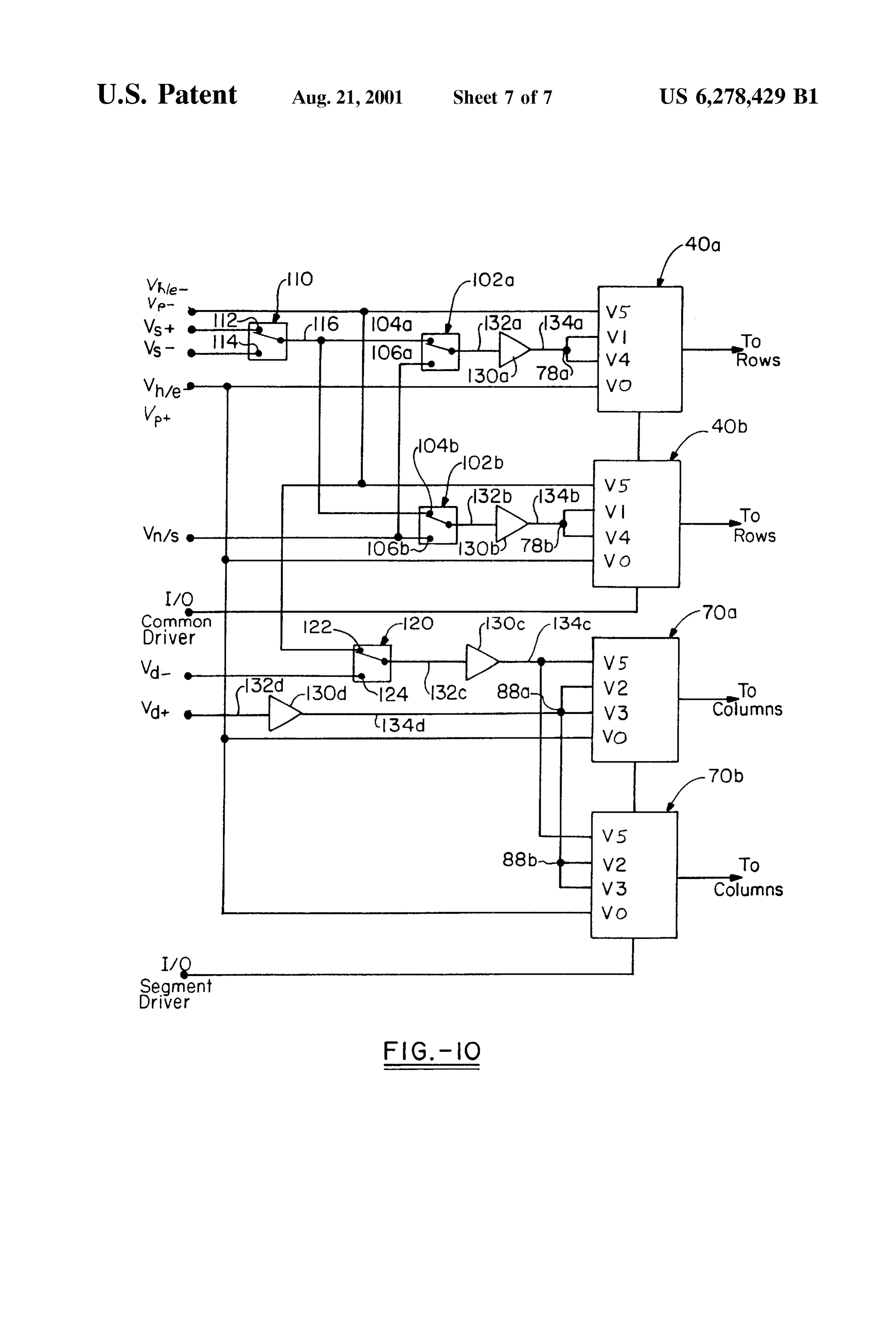
plurality of electrodes, each common driver having a first FIG. 8 is a block diagram for a segment driver employed and a Second common frame Switch, each common frame in a driving circuit of the present invention; Switch having a high input and a low input, first and Second FIG. 9 is a four by four pixel display showing how such frame Switches linked to one another by a common frame 25 a display would appear according to the waveforms pro line, the frame Switch outputs connected to a plurality of vided in FIGS. 6-8; and common data Switches, each common data Switch having an FIG. 10 is a block diagram according to the present output, the first common frame Switch receiving a first and a Second common Voltage input and the Second common invention showing both common and Segment drivers. frame Switch receiving a third and a fourth common Voltage BEST MODE FOR CARRYING OUT THE input connected to each other, wherein the common frame INVENTION line is toggled to Selectively pass through the common
Voltage inputs for use as the common Voltage output from The present invention is employed with cholesteric liquid each common data Switch, and at least one Segment driver crystal displays which in and of themselves are quite simple coupled to the Second plurality of electrodes, at least one 35 to manufacture. These displays are typically opposed Sub Segment driver having a plurality of Segment Voltage outputs Strates of either glass or plastic. Patterned indium tin oxide which are Selectively applied to the Second plurality of electrodes are disposed on one Substrate as common/row electrodes to drive the cholesteric liquid crystal material to electrodes and are disposed on the other Substrate as a desired texture. Segment/column electrodes. The common and Segment elec Yet other aspects of the present invention are attained by 40 trodes are positioned in different directions with respect to a method for addressing a liquid crystal display having a one another to form pixels which can be individually plurality of common electrodes oriented differently with addressed by applying Voltages to both. The indium tin respect to a plurality of Segment electrodes with cholesteric oxide is usually overlaid with a barrier coat and an alignment liquid crystal material disposed therebetween, the method layer. Spacing between the Substrates is typically between 4 comprising the Steps of connecting at least one common 45 tim to 5 lum. Commercially available materials and Standard driver to the plurality of common electrodes, connecting at fabrication techniques are employed to manufacture the least one Segment driver to the plurality of Segment displayS.
electrodes, and toggling a pair of frame Switches in each AS noted in the Background Art, cholesteric displays are common and Segment driver Such that a first of the pair of typically driven into the homeotropic texture by applying frame Switches applies one of two waveforms to the corre 50 bipolar waveforms, average value of about 50–60 Vs, to sponding electrodes or Such that a Second of the pair of a plurality of rows with high Voltage electronics. Given the frame Switches applies an arbitrary waveform to the corre unipolar output range of Super twisted nematic driver chips sponding electrodes. (nominally 0-40 volts), it was evident that the dynamic drive These and other objects of the present invention, as well Scheme would need to be revised to a differential drive as the advantages thereof over existing prior art forms, 55 Scheme. In other words, the necessary large RMS voltages which will become apparent from the description to follow, can only be generated acroSS the display by proper combi are accomplished by the improvements hereinafter nation of large amplitude row and large amplitude column described and claimed. waveforms. Moreover, the display design had to be modified
BRIEF DESCRIPTION OF THE DRAWINGS
to lower the maximum RMS voltage required to drive the 60 display into the homeotropic texture to about 40 volts. Yet
For a complete understanding of the objects, techniques another limitation of STN driver chips is that their logic and structure of the invention, reference should be made to allows only two of the four display Voltage inputs to be the following detailed description and accompanying applied to a display at one time by a single driver chip. drawings, wherein: Accordingly, the dynamic drive scheme shown in FIGS. 2A FIG. 1 is a Schematic representation of the various tex 65 and 2B needed to be modified to “fit onto the common/row tures of a cholesteric liquid crystal as they appear in a driver chips by breaking it into two parts. The first part of display; this modified dynamic drive Scheme applied V. reparation tO
Page 12
all pixels in all rows Simultaneously, driving the entire driver's display Voltage inputs can be routed to the driver's display into the homeotropic texture. The Second part begins outputs. AS Such, the “Switches' drawn in the figure are not by applying a “holding Voltage (whose value is less than real, physical Switches, but they do represent the function Vpreparation) to all pixels not being addressed in order to ality of the circuitry of the driver. maintain their homeotropic textures until those pixels can be In FIG. 6, a common driver according to the present addressed. This “break up’ of the dynamic drive scheme is invention is generally indicated by the numeral 40. As implemented by having the common driver chips function in shown, the driver 40 can be thought of as an analog one of three operating modes while requiring the Segment multiplexer with four voltage inputs and anywhere from 80 driver chips to function in one of two additional operating to 160 outputs. For simplicity Sake, only four outputs are modes. shown in the drawing. In FIG. 6, the common driver 40 has The most Significant consequence of breaking up the four inputs which are arbitrarily designated as Vo, Vs, V, original dynamic drive Scheme is the addition of a new and V.
application voltage to the RMS pixel waveform in order to The common driver 40 includes a pair of frame Switches “hold” the cholesteric liquid crystal material in the homeo 42 wherein each frame Switch has an alphabetic Suffix. As Such, the common driver 40 has a frame Switch 42a and a tropic texture after applying the preparation voltage V. AS 15 frame seen in FIGS. 3A and 3B, the evolution voltage is now Switch 42b. Each frame Switch 42 incorporates a high provided along with a holding Voltage which is designated input 44 and a low input 46. As such, the frame switch 42a as V. Accordingly, a pixel sees a voltage waveform that has a high input 44a and a low input 46a. The frame produces a sequence of four RMS voltages, Va., Switches 42a and 42b are coupled to one another by a frame Vholas Vselectinon-selece and Vevolve Vheld is a Voltage value line 48 which is ultimately controlled by a digital control that is applied to a pixel in the homeotropic texture prior to circuit (not shown) that may include a microprocessor. It it being addressed with V. In other Words, a will be appreciated that the digital control circuit associated pixel waveform is the resulting waveform produced at any with the driver chips contains the necessary hardware, pixel by combining output waveforms at the respective Software and memory to fully implement the objects of the electrodes. All other RMS voltages shown in FIGS. 3A and 25 present invention.
B Serve the same function as they did for the original Connected to the outputs of each frame Switch 42 are a dynamic drive Scheme. All of the Voltage values associated plurality of data switches 50, each of which has an alpha with the drive Scheme are dependent upon the particular betic suffix. Each data Switch 50 has a high input 52 and a cholesteric material used and the design of the display. AS low input 54, both of which have a corresponding alphabetic Such, any Voltage value discussed herein is exemplary and suffix. Selection of the high input 52a or low input 54a is not meant to be limiting. controlled by a data shift register within the driver and the The drive Scheme of the present invention requires the data shift register is ultimately controlled by the digital common driver chips to function in one of three operating control circuit. Depending upon the input Voltages, the modes and the Segment driver chips to function in one of two toggling of the frame line 48 and the data bits controlling the additional operating modes as Seen in FIG. 4. In each 35 data Switches 50, a data output 56 with a corresponding operating mode, the driver chips apply different monopolar alphabetic Suffix is generated by each data Switch. component output waveform combinations to the display A modification to the common driver 40, which allows electrodes. The common and Segment input preparation implementation of the dynamic drive Scheme, is attained by waveforms are simply Square waves running rail to rail and electrically connecting the Voltage inputs V2 and V of are not shown. The two Segment operating waveforms are 40 frame Switch 42b to one another to form a super input 58. Segment Select and Segment non-Select. The three common The Super input 58 allows an arbitrary waveform that input operating waveforms are common hold/evolve, com conforms to the display Voltage input rules mentioned in the mon Select, and common non-Select. Those skilled in the art Background Art to be piped to a single output or to multiple will appreciate that the RMS value of the hold/evolve and outputs of the common driver 40 while the other outputs of data waveforms provided to the pixel are properly indepen 45 the driver 40 Swing rail to rail as the frame line 48 is toggled. dent of the Segment waveforms. Combination of the input If the receiving data Switch 50 is set to a high input 52, the waveforms shown in FIG. 4 generate the Segment output data output 56 will be either voltage input Vo or Vs., waveform shown in FIG. 5A, the common output waveform depending upon the state of the frame line 48. If the shown in FIG. 5B, and the pixel waveform shown in FIG. receiving data Switch 50 is set to the low input 54, the data 5C. The pixel waveform is a result of the difference between 50 output will be the arbitrary waveform applied to the Super the common and Segment waveforms. Accordingly, the pixel input 58, regardless of the state of the frame line 48. is prepared, held, written to, evolved, and then turned off, The common driver 40 presented in FIG. 6 is employed whereupon the desired appearance of the pixel is displayed. in a “scan mode” that updates the display row by row. The Referring now to FIGS. 6-8, implementation of the input, particulars of this mode are discussed below. In order to output and resulting pixel waveforms for cholesteric dis 55 implement this mode, three different Voltage values (V, playS is accomplished by using Standard, off-the-shelf, low V, V) must be supplied to the Super input 58. cost Super twisted nematic drivers. FIGS. 6-8 are simply Referring now to FIG. 7, it can be seen that the common graphical representations of the functionality of the driver driver 40 may also receive a 2-level select waveform at the chips for Selectively transmitting input waveforms (shown to Superinput 58. This allows for a “flash mode update' the left of the chip) to obtain the desired output waveforms 60 wherein the entire image appears on the display all at once. (shown to the right of the chip). The output waveforms from The Superinput 58 receives either a voltage value of V+ or row/column driver(s) and the column/Segment drivers are V- during the Selection phase. The particular aspects of this then combined at the pixel to form the pixel waveforms. The mode are also discussed below. In all other respects, the drivers shown herein are not meant to be an accurate common driver shown in FIG. 7 is substantially the same as representation the internal design or construction of an STN 65 the common driver shown in FIG. 6. driver. Rather, these block diagrams are meant to be a Referring now to FIG. 8, a Segment driver designated representation of the logic of the driver showing how the generally by the numeral 70, is presented. The Segment
Page 13
driver 70 is employed in either the scan mode or the flash The logic of the STN common driver prevents the simul mode. While the row or common electrodes apply the taneous output of the common preparation waveform and majority of the pixel waveform, the Segment or column any other common output waveform on a single driver. output waveforms Supply the data that combines with the Consequently, in order to generate properly the prepara row Select waveform during the Select phase to apply a high tion phase of the pixel waveform, all segment driver outputs or low Selection Voltage value to the pixel. Accordingly, the must apply the Segment preparation waveform to the Seg cholesteric liquid crystal material is driven to the texture ment electrodes while all common driver outputs are apply corresponding to the high or low Selection data Voltage. ing the common preparation waveform to the common The segment driver 70, much like the common driver 40, electrodes. This requirement holds regardless of the number includes frame Switches 72a and 72b, each of which has a of common or segment STN drivers connected to a bistable high input 74 and a low input 76 with corresponding cholesteric liquid crystal display. alphabetic Suffixes. The frame Switches 72a and 72b are coupled to one another by a frame line 78. Receiving the The common driver 40 initially controls application of the output generated by the frame Switches 72 are data Switches preparation phase by Setting the data Switches 50 to the high 80, each of which has an alphabetic suffix. The data Switches 15 input to receive the preparation voltage V+ or V-. As best 80 each have a high input 82 and a low input 84, wherein Seen in the common or row output waveforms, the prepa each output 86 has a corresponding alphabetic Suffix. AS ration section shows application of V+ or V-. This is with the common drivers, the segment driver 70 contains a accomplished by toggling frame Switch 42a between its high data shift register that controls the Selection of the high input and low inputs, with all the data Switches 50 toggled to their 82 or the low input 84 of the data Switches 80. Toggling of high input 52. During this phase, the segment driver 70 the frame line 78 and setting of the data Switches 80 is outputs V or V, to the segment or column electrodes. AS ultimately controlled by the digital control circuit. The a result, the difference between the interSecting common and voltage input Vo receives preparation voltage V+ while Segment electrodes is applied to the pixel. In particular, the voltage input Vs receives preparation voltage V- or data frame Switch 72 is toggled between the high input 74 and the Voltage V-. Inputs V2 and V are electrically connected to 25 low input 76, with all the data Switches 80 toggled to their form Superinput 88 that receives data voltage V+. The high input 82.
digital control circuit associated with the driving circuit In the hold/select/evolve section of the common or row Sequences application of the various Segment waveforms in output waveforms, it can be seen that initially row 0 receives much the same manner as the common waveforms. AS Seen one cycle of V+ and V.- from the Superinput 58 by virtue in the resulting Segment waveforms for the corresponding of the data Switch 50a being toggled to the low input 54a. outputs of the data Switches 80, the preparation voltages are Simultaneously, all other data Switches are toggled to their applied during the preparation phase while the data Voltages respective high inputs 52 to receive either V, or Vb are applied thereafter. Accordingly, depending upon whether depending upon toggling of the frame line 48 that places the the data voltage applied is V- or V+, simultaneous with frame Switch 42a at either the high input 44a or the low input the application of the Selection voltages to the row 35 46a. Once the application of the Selection Voltage is com electrodes, the resulting planar or focal conic textures are plete for row 0, the data Switch 50a is then set to the high obtained. input 52a So that the evolution phase may begin. Upon The digital control circuit controls the Sequencing of the completion of the application of the Selection Voltage to row common and Segment drivers to obtain the desired image 0, data Switch 50b is set to the low input 54b to apply V. appearance. AS Seen in FIGS. 6-8, the digital control circuit 40 and V for one cycle to row 1. The above process is then controls the drivers 40 and 70 to simultaneously apply the repeated to complete the hold/Select/evolve Section of the preparation Voltages during a first phase, the hold/Select/ waveform for row 1 and the remaining rows. During this evolve and data Voltages during a Second phase and the phase, the Segment driver 70 outputs V or V to the evolve, non-Select and pseudo data Voltages during a third Segment or column electrodes. In particular, the data phase. 45 Switches 80 are toggled between their high inputs 82 and low It must be stated at this time that the only way for all inputs 84, as selectively determined by the digital control pixels in all rows of a bistable cholesteric display to be circuit, to apply either V and V in the appropriate properly prepared (driven into the homeotropic texture) is Sequence to the columns 0–4 during application of V and for those pixels to be driven into the homeotropic texture V by the common driver 40 to obtain the desired appear simultaneously. This simultaneity is mandated by the dif 50 ance of all pixels in the row being addressed. ferential nature of the revised dynamic drive Scheme and the Upon completion of the hold/Select/evolve phase, frame SIN driver logic. Switches 42 are toggled between high inputs 44 and low The only way to generate the necessary large RMS inputs 46 for a predetermined period for application of V, Voltages of the preparation phase of the pixel waveform is whereupon data Switches 50 are toggled to a low input and for the Segment driver 70 to apply the Segment preparation 55 V, is applied to the rows in the Scan mode. Shortly after waveform to the Segment electrodes while the common Voltage V, is applied, all pixels in the row display the driver 40 applies the common preparation waveform to the desired texture. AS can be seen in row 1 of the output common electrodes. Once the segment driver 70 begins waveforms, the application of V+ and V- is one segment applying the data waveforms to the Segment electrodes, the cycle and one-half common cycle removed from the appli preparation phase of the pixel waveform is no longer gen 60 cation of V and V in the row 0 output. Likewise, the erated even if the common driver 40 still applies the com application of V and V in the outputs of rows 2 and 3 are mon preparation waveform to the common electrodes. removed from the preceding row by the same amounts Likewise, if the common driver 40 begins applying the during the hold/Select/evolve phases.
hold/evolve waveform, the select waveform, or the non One requirement of any liquid crystal display drive Select waveform, the preparation phase of the pixel wave 65 Scheme is that the time-averaged Voltage on every pixel be form is no longer generated even if the segment driver 70 about 0 when averaged over Some number of image updates. Still applies the Segment preparation waveform. If the time average Voltage acroSS a pixel is not 0, ions in the
Page 14
liquid crystal material will migrate toward the electrodes. Minimum Evolution Time=(Number of outputs per row chip This ion migration will Screen the Voltage appearing on the 1)*(Row Select Time) pixel’s electrodes, reduce the effective Voltage across the In the flash mode, the pixels in each row experience an pixel and change the Switching properties of the pixel. evolution time that depends on when the row was addressed Additionally, the electrodes can be permanently damaged if and hence on the total number of rows in the display. The the migrating ions reach the electrodes. These changes are waveform fed to the Superinput 58 is only two-level and only performs the Select function by applying V or V. All usually observed as image retention from one display update rows to the next. The dynamic drive scheme employed by the evolve until the last row addressed receives the mini driving circuit of the present invention accomplishes this 0 mum evolve time necessary, which depends on the choles average over two image updates by changing the phase of teric liquid crystal material used. After the evolution of the the hold/evolve waveform between 0 and 180 degrees on final row addressed is complete, all rows and columns are every image update. A 0-degree hold/evolve waveform taken to an equal potential resulting in the Voltage acroSS begins high and halfway through its cycle changes to low. each pixel being driven to 0. Consequently, the image Conversely, a 180-degree hold/evolve waveform begins low appears all at once on the display.
and halfway through its cycle changes to high. AS can be 15 Flash mode addressing yields an image update with the seen in FIG. 6, rows 1 and 3 develop a non-0 DC offset following appearance. First, the whole display is black for because the number of high half-cycles is not equal to the the duration of the preparation time plus the row Select time number of low half-cycles during the hold/evolve phases. times the total number of rows plus the minimum evolution Specifically, row 1 has three high half-cycles and two low time. Next, the whole image appears on the display at once, half-cycles, and row 3 has four high half-cycles and three with all planar pixels relaxing into their final reflective States low half-cycles. On the next image update the phase of the Simultaneously. The transparent focal conic pixels have hold/evolve waveform is changed 180 degrees so that row 1 already reached their final transparent Stable States by the will have two high half-cycles and three low half-cycles and end of the evolution time and do not change their appear
row 3 will have three high half-cycles and four low half cycles. Consequently, over two image updates a given row 25 Employing the Segment and common drivers of the present invention, the following exemplary Voltage values has an equal number of high and low half-cycles, and hence have a 0 time-averaged voltage and 0 DC offset. Rows 0 and 2 been determined:
naturally have 0 DC offset regardless of the phase of the hold/evolve waveform because the number of high half cycles is always equal to the number of low half-cycles Abbreviation Description Typical Value during the hold/evolve phases. Specifically, row 0 has two high half-cycles and two low half-cycles while row 2 has V+ Upper level Preparation waveform 40 V three high half-cycles and three low half-cycles. V- Lower level Preparation waveform OV Ve+ Upper level Hold/Evolve waveform 40 V
As seen in FIG. 9, the combination of the output wave Ve- Lower level Hold/Evolve waveform 4V forms in FIG.8 with the output waveforms of either FIG. 6 35 V-
V+ Upper level Select waveform
Lower level Select waveform
or FIG. 7 forces the material into focal conic textures for all column 0 pixels. Column 1 pixels are all focal conic except V+ V-
Upper level Data waveform
Lower level Data waveform
for row 1. While in column 2, all the pixels are focal conic Vin's Row Non-Select voltage for Scan Mode 22 V except for row 0. In column 3, all the pixels are planar except for row 3. After application of the data Voltages necessary to 40 The relationship between these row and column wave generate an image, a pseudo data Voltage waveform is applied to the column electrodes while the evolve/non-Select form levels and the pixel voltage RMS values are as follows: Preparation RMS Voltage:
phase is applied to the row electrodes.
When the scan mode is desired, the waveform fed to the
Superinput 58 is three-level (V, V, V) and performs 45 Hold/Evolve RMS Voltage:
either the row Select function or the row non-Select function.
The duration of the evolution phase is the same for all rows and the image update has the following appearance. First, VeV+ -Vthe entire display is black for the duration of the preparation 50 Planar Texture Select Phase RMS Voltage (Column Data out time plus the evolution time occurring after the pixels in the of phase with Row Select waveform): first row are addressed. Upon completion of the evolution Vet-(V+ -V-)+(V- -V+)''/sqrt(2) phase, the pixels in the first row relax into their final stable Focal Conic Texture Select Phase RMS Voltage (Column States. Likewise, all the pixels in the Second row addressed Data in phase with Row Select waveform: relax into their final Stable States. These StepS are then 55 Vi?-(V+ -V+)+(V- -V-)''/sqrt(2) repeated until the pixels in all the addressed rows have In order to guarantee no DC offset acroSS all the pixels in the arrived into their final reflective planar or transparent focal display over two image updates, the following rules must conic textures. After the evolution of the final row addressed apply to the Voltage levels: is complete, all rows and columns are taken to an equal potential resulting in the Voltage acroSS pixel being driven to
O. 60
The total amount of time for the image update can be V+ - V = V - VI-. determined by the following equation:
Scan mode update time=Preparation Time--(Row Select Referring now to FIG. 10, it can be seen that a driving Time)*(Total Number of Rows)+Evolution time 65 circuit block diagram is designated generally by the numeral The minimum possible evolution time, given that all rows 100. The driving circuit 100 includes a plurality of common have equal Select times is determined by: drivers 40 and a plurality of segment drivers 70.
Page 15
The circuit produces the common and Segment driver What is claimed is:
input waveforms of FIGS. 6, 7, and 8. Take note that this 1. A bistable cholesteric liquid crystal display, compris block diagram is not meant to be an accurate representation ing:
the design or construction of the drive circuit. Rather, it is a pair of opposed Substrates, one Said Substrate having a meant to be a representation of the logic of the drive circuit first plurality of electrodes, the other said substrate showing how the DC voltages may be routed to the common having a Second plurality of electrodes oriented in a and Segment drivers display Voltage inputs. direction different than said first plurality of electrodes; The Voltages V, V, V, V, V, V, and V, are a cholesteric liquid crystal material disposed between Said DC voltages whose values and relationships have been pair of opposed Substrates and forming a pixel at each previously Stated. interSection of Said first and Second plurality of elec A plurality of buffers 130a-d are coupled to the drivers trodes;
40a-b and 70a-b and have voltage inputs 132 that are a first Super twisted nematic driver having a plurality of isolated from their voltage outputs 134 and thus serve to outputs connected to Said first plurality of electrodes, keep the Voltages applied to the inputs 132 from varying and when a load is applied to the outputs 134 (i.e., the buffer 15 a Second Super twisted nematic driver having a plurality inputs are high impedance while the outputs are low of outputs connected to Said Second plurality of impedance). The buffers 130 ensure that the proper voltage electrodes, wherein both Said driverS receive a plurality values are maintained throughout the drive circuit as the of Voltage waveforms for Selective transmission as display is updated. respective Voltage output waveforms to Said first and A pair of mode select Switches 102a–b are connected to Second plurality of electrodes. corresponding drivers 40a-b to determine in which mode 2. The display according to claim 1, wherein Said Voltage the corresponding common driver operates, whether in the output waveforms are combined to form a pixel waveform hold/select/evolve mode or the evolve/non-select mode. All at each said pixel.
mode select switches 102 are independent of each other and 3. The display according to claim 2, wherein Said pixel are ultimately controlled by the digital control circuit. When 25 waveform comprises:
the mode select Switch 102a is set to a high input 104a, the a preparation phase for applying a preparation Voltage to Select common input waveform is routed to the input 132a, each Said pixel for driving Said cholesteric liquid crys through the buffer 130a, and onto the common driver 40a. tal material into a homeotropic texture; In particular, the buffer 130 generates an output 134 that is a hold phase for applying a hold Voltage, different than received by the Superinput 78. When the Switch 102a is set Said preparation Voltage, for maintaining Said choles to the low input 106a, the input non-select DC voltage V, teric liquid crystal material in the homeotropic texture; is routed to the input 132a, through the buffer 130a, and onto the common driver 4.0a in a like manner. a Selection phase for applying a Selection Voltage to each A common Select waveform generator Switch 110 creates Said pixel for predisposing Said cholesteric liquid crys the Select common input waveform that has been previously 35 tal material; and described. It consists of a high input 112 connected to V, an evolution phase for applying an evolution Voltage to a low input 114 connected to V, and an output 116 each said pixel to allow Said predisposed liquid crystal connected to the high inputs 104 of the mode select switches material to relax into either a planar or a focal conic 102. It is ultimately controlled by the digital control circuit. teXture.
Toggling the common Select waveform generator Switch 110 40 4. The display according to claim 1, wherein Said plurality between the high input 112 and the low input 114 generates of Voltage input waveforms applied to one of Said drivers the select common input waveform at the output 116 by comprises an upper level and a lower level preparation alternately routing the Voltages VS-- and VS- to the output waveform, an upper level and a lower level Select waveform, 116. and an upper and a lower level hold/evolve waveform. A prep/write select Switch 120 consists of a high input 122 45 5. The display according to claim 4, wherein Said plurality connected to V, a low input 124 connected to V, and of Voltage input waveforms applied to one of Said drivers an output 126 connected to the buffer input 132c. It is comprises a non-Select waveform.
ultimately controlled by the digital control circuit. During 6. The display according to claim 1, wherein Said plurality the preparation phase of an image update the prep/write of Voltage input waveforms applied to one of Said drivers comprises a lower level preparation Voltage and an upper switch 110 is set to the high input 122 and V is routed to 50 level the buffer 132 and on to the segment drivers. During the and a lower level data waveform. Writing phase of an image update the prep/write Switch 110 7. The display according to claim 1, wherein Said Voltage is set to the low input 124 and V is likewise routed to the output waveforms applied to one of Said plurality of elec buffer 132 and on to the segment drivers 70. trodes comprises:
Although the Superinputs 88 are used on the Segment 55 an alternating upper and lower level preparation drivers in the current invention, it is not necessary. All that waveform, an alternating upper and lower level Select is necessary is that V be less than or equal to V2. The V waveform, and an alternating upper and lower level Voltage input is never used with the current waveforms. hold/evolve waveform.
Thus, it can be seen that the objects of the invention have 8. The display according to claim 7, wherein Said Voltage been satisfied by the structure and its method for use 60 output waveforms applied to one of Said plurality of elec presented above. While in accordance with the Patent trodes further comprises a non-Select waveform. Statutes, only the best mode and preferred embodiment has 9. The display according to claim 1, wherein Said Voltage been presented and described in detail, it is to be understood output waveforms applied to one of Said plurality of elec that the invention is not limited thereto or thereby. trodes comprises:
Accordingly, for an appreciation of true Scope and breadth 65 an alternating upper and lower level preparation of the invention, reference should be made to the following waveform, and an alternating upper and lower level claims. data waveform.
Page 16
10. A method for addressing a cholesteric liquid crystal bistable cholesteric liquid crystal material disposed therebe display which has a pair of opposed Substrates, one of the tween form a plurality of pixels, the driving circuit Selec Substrates having a first plurality of electrodes, the other tively applying Voltages to the first and the Second plurality Substrate having a Second plurality of electrodes oriented in of electrodes to control the appearance of each pixel, the a direction different than the first plurality of electrodes, the 5 driving circuit comprising:
Substrates having cholesteric liquid crystal material disposed at least one common driver coupled to the first plurality of therebetween to form a pixel at each intersection of the first electrodes, each common driver having a first and a and the Second plurality of electrodes, the first plurality of Second common frame Switch, each said common electrodes having at least a first driver coupled thereto and frame Switch having a high input and a low input, Said the Second plurality of electrodes having at least a Second first and Second frame Switches linked to one another driver coupled thereto, the method comprising the Steps of: by a common frame line, Said high and low inputs applying a plurality of Voltage input waveforms to the first connected to a plurality of common data Switches, each driver and the Second driver, wherein Said Voltage input having a common output, Said first common frame waveforms are about 60 volts RMS or less; Switch receiving a first and a Second common Voltage Selectively transmitting Said plurality of Voltage input 15 input and Said Second common frame Switch receiving waveforms through the first and the second drivers to a third and a fourth common Voltage input connected to generate respective first and Second output waveforms, each other, wherein Said common frame line is toggled to Selectively pass through Said common Voltage inputs combining Said first and Second output waveforms at the for use as Said common Voltage output from each Said interSecting electrodes to generate a pixel waveform common data Switch; and that drives the cholesteric liquid crystal material to the at least one Segment driver coupled to the Second plurality desired appearance, wherein Said Step of combining of electrodes, Said at least one Segment driver having a further comprises the Steps of plurality of Segment Voltage outputs which are Selec applying preparation Voltages to each pixel for driving the tively applied to the Second plurality of electrodes to cholesteric material into a homeotropic texture; 25 drive the cholesteric liquid crystal material to a desired applying hold Voltages to each pixel wherein at least one teXture.
of Said hold Voltages is different than Said preparation 17. The driving circuit according to claim 16, wherein Voltages, to maintain the cholesteric material in the Said at least one Segment driver has a first and a Second homeotropic texture; Segment firmed Switch, each said Segment frame Switch applying Selection Voltages to each pixel for predisposing having a high input and a low input, Said first and Second the cholesteric material; and Segment frame Switches linked to one another by a Segment applying evolution Voltages to each pixel to allow the frame line, Said high and low Segment inputs connected to a plurality of Segment data SWitches, each Segment data predisposed cholesteric material to relax into either a Switch having a Segment output, Said first Segment frame planar or a focal conic texture.
11. The method according to claim 10, wherein said step 35 Switch receiving a first and a Second Segment Voltage input and Said Second Segment frame Switch receiving a third and of applying further comprises the Steps of applying an upper level and a lower level preparation wherein a fourth Segment Voltage input connected to each other, Said Segment frame line is toggled to Selectively waveform; pass through said Segment Voltage inputs for use as Said applying an upper level and a lower level Select wave 40 Segment Voltage output.
form; and 18. The driving circuit according to claim 17, wherein applying an upper level and a lower level hold/evolve Said third and fourth common Voltage inputs provide a first waveform. arbitrary waveform for Said corresponding common Voltage 12. The method according to claim 11, wherein Said Step output, and wherein Said third and fourth Segment Voltage of applying further comprises the Step of: 45 inputs provide a Second arbitrary waveform for Said corre applying a non-Select waveform. Sponding Segment Voltage output. 13. The method according to claim 10, wherein said step 19. The driving circuit according to claim 18, wherein of Selectively transmitting further comprises the Steps of: Said first common frame Switch receives a preparation transmitting upper and lower level preparation wave Voltage and a hold/evolve voltage.
forms, 50 20. The driving circuit according to claim 18, wherein transmitting upper and lower level Select waveforms, and Said age first Segment frame Switch receives a preparation Volt and a data Voltage.
transmitting upper and lower level hold/evolve wave 21. The driving circuit according to claim 18, wherein forms. Said Second common frame Switch receives at least a Selec 14. The method according to claim 13, wherein said step of Selectively transmitting further comprises the Step of 55 tion22.Voltage.
The driving circuit according to claim 18, wherein transmitting a non-Select waveform. Said Second Segment frame Switch receives a data Voltage. 15. The method according to claim 10, wherein said step 23. The driving circuit according to claim 18, wherein of Selectively transmitting further comprises the Steps of: said second row frame Switch receives three different volt transmitting upper and lower level preparation wave 60 age values So that indicia appears on the display row by row. forms, and 24. The driving circuit according to claim 18, wherein transmitting upper and lower level data waveforms. Said Second common frame Switch receives two different 16. A driving circuit for a reflective bistable cholesteric Voltage values So that indicia appears on the display all at liquid crystal display which includes one Substrate having a OCC.
first plurality of electrodes opposed by another Substrate 65 25. A method for addressing a liquid crystal display having a Second plurality of electrodes, wherein the inter having a plurality of common electrodes orthogonally posi section of the first and the second plurality of electrodes with tioned with respect to a plurality of Segment electrodes with
Page 17
cholesteric liquid crystal material disposed therebetween, 32. The method according to claim 26, further comprising the method comprising the Steps of the step of:
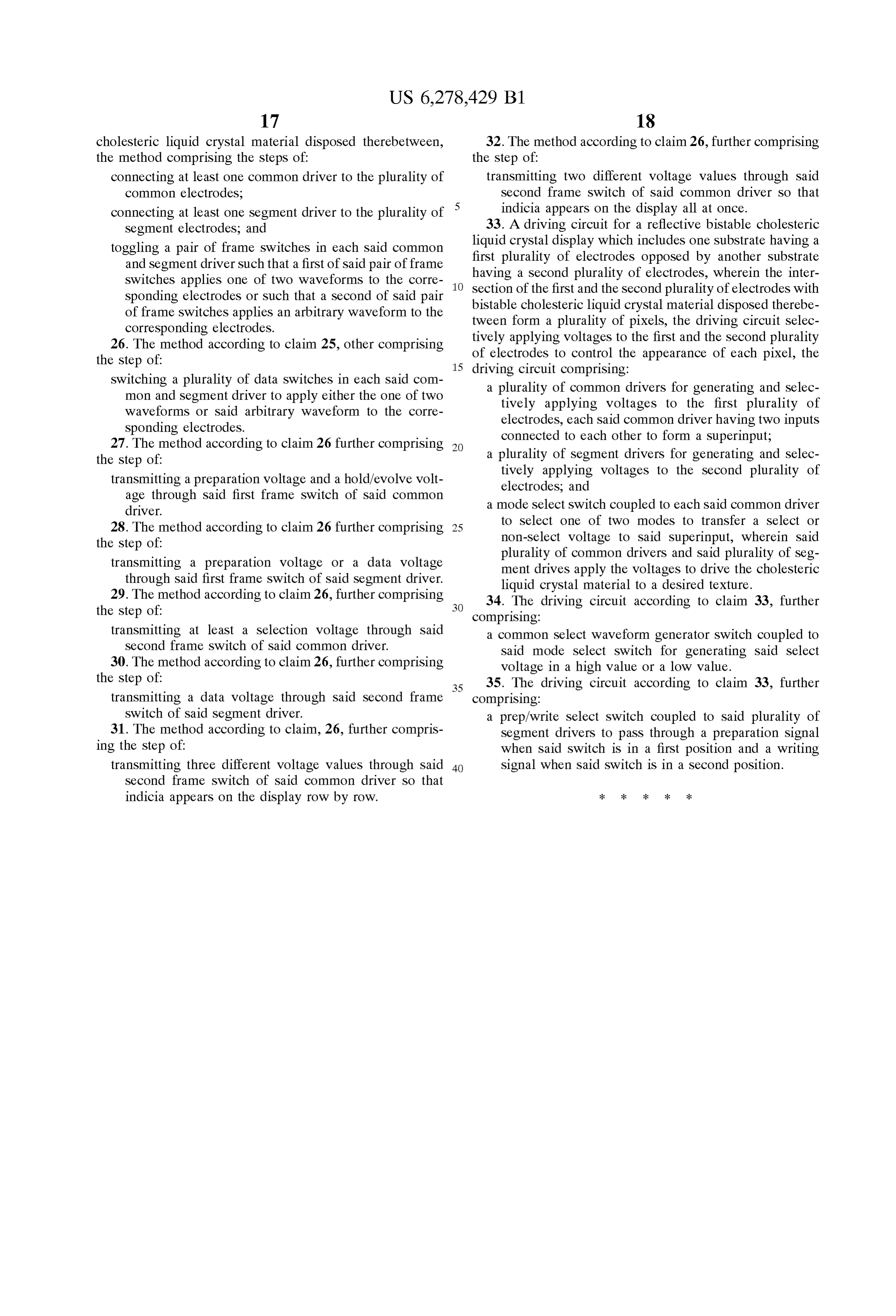
connecting at least one common driver to the plurality of transmitting two different Voltage values through Said common electrodes, Second frame Switch of Said common driver So that connecting at least one Segment driver to the plurality of 5 indicia appears on the display all at once. Segment electrodes, and 33. A driving circuit for a reflective bistable cholesteric toggling a pair of frame Switches in each Said common liquid first crystal display which includes one Substrate having a plurality of electrodes opposed by another Substrate and Segment driver Such that a first of Said pair of frame having a Second
Switches applies one of two waveforms to the corre section of the firstplurality of electrodes, wherein the inter sponding electrodes or Such that a Second of Said pair bistable cholesteric liquid crystal plurality and the second material of electrodes with disposed therebe of frame Switches applies an arbitrary waveform to the tween form a plurality of pixels, the driving circuit Selec corresponding electrodes. tively applying Voltages to the first and the Second plurality 26. The method according to claim 25, other comprising of electrodes to control the appearance of each pixel, the the step of: 15 driving circuit comprising:
Switching a plurality of data Switches in each Said com a plurality of common drivers for generating and Selec mon and Segment driver to apply either the one of two tively applying Voltages to the first plurality of waveforms or said arbitrary waveform to the corre electrodes, each Said common driver having two inputs sponding electrodes. connected to each other to form a Superinput; 27. The method according to claim 26 further comprising the step of: a plurality of Segment drivers for generating and Selec transmitting a preparation Voltage and a hold/evolve Volt tively applying Voltages to the Second plurality of age through Said first frame Switch of Said common electrodes, and driver. a mode Select Switch coupled to each Said common driver to Select one of two modes to transfer a Select or 28. The method according to claim 26 further comprising 25 non-Select Voltage to Said Superinput, wherein Said the step of: plurality of common drivers and Said plurality of Seg transmitting a preparation Voltage or a data Voltage ment drives apply the Voltages to drive the cholesteric through Said first frame Switch of Said Segment driver. liquid crystal material to a desired texture. 29. The method according to claim 26, further comprising 34. The driving circuit according to claim 33, further the step of: comprising:
transmitting at least a Selection Voltage through Said a common Select waveform generator Switch coupled to Second frame Switch of Said common driver. Said mode Select Switch for generating Said Select 30. The method according to claim 26, further comprising Voltage in a high value or a low value. the step of: 35 35. The driving circuit according to claim 33, further transmitting a data Voltage through Said Second frame comprising:
Switch of Said Segment driver. a prep/write Select Switch coupled to Said plurality of 31. The method according to claim, 26, further compris Segment drivers to pass through a preparation Signal ing the Step of: when said Switch is in a first position and a writing transmitting three different Voltage values through Said 40 Signal when Said Switch is in a Second position. Second frame Switch of Said common driver So that indicia appears on the display row by row. k k k k k
Page 18
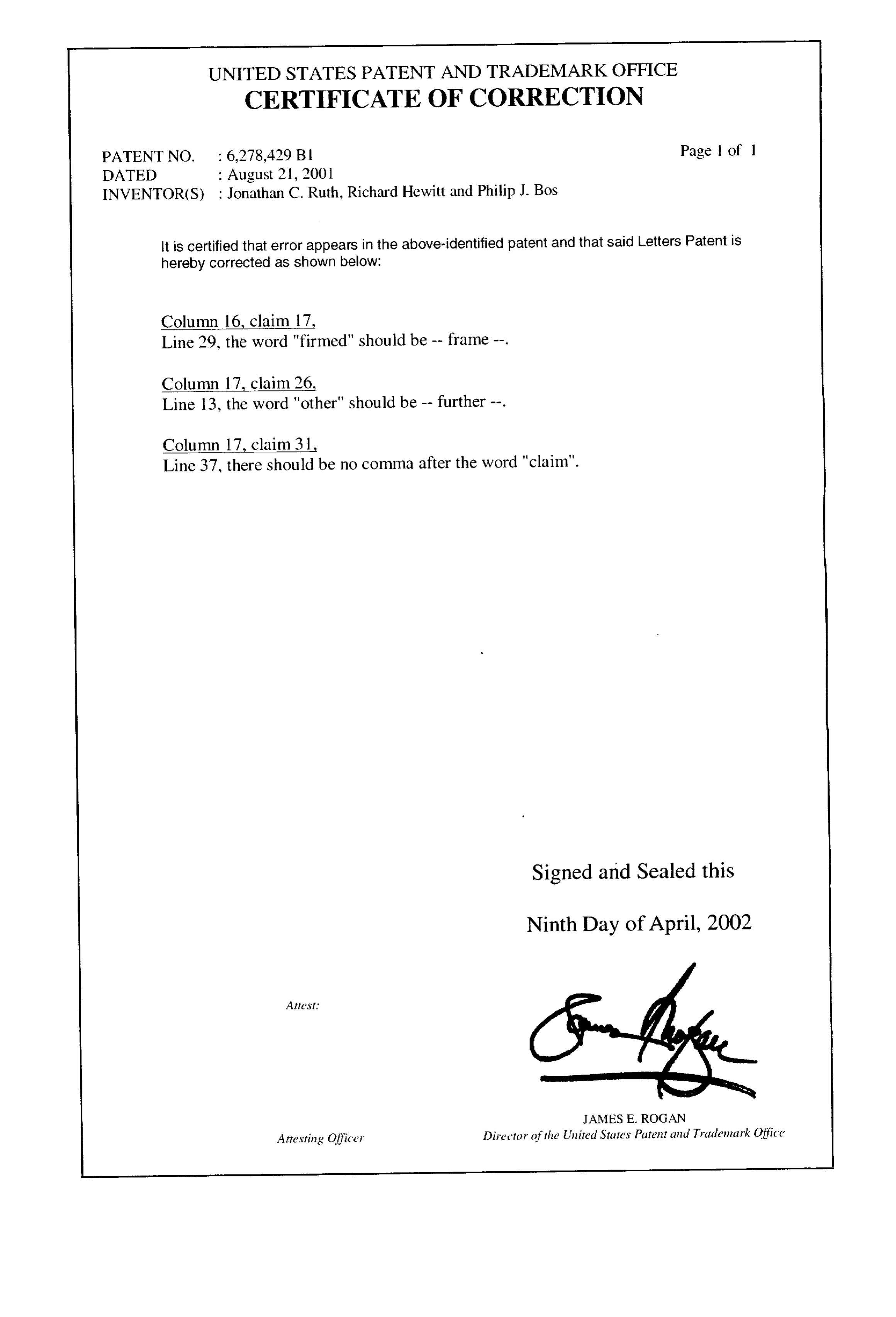
UNITED STATES PATENT AND TRADEMARK OFFICE
CERTIFICATE OF CORRECTION
PATENT NO. : 6,278.429 Bl Page 1 of 1
INVENTOR(S) : Jonathan C. Ruth, Richard Hewitt and Philip J. Bos It is certified that error appears in the above-identified patent and that said Letters Patent is hereby corrected as shown below:
Column 16, claim 17,
Line 29, the word "firmed" should be -- frame --.
Column 17 claim 26
Line l3, the word "other" should be -- further --. Column 17, claim 31
Line 37, there should be no comma after the word "claim". Signed and Sealed this
Ninth Day of April, 2002
Attest:
JAMES E ROGAN
Attesting Officer Director of the United States Patent and Trademark Office
Provenance
- Collection
- Cited prior art
- Original PDF
- patentimages.storage.googleapis.com →
- Filed
- 1998-09-11
- Pages
- 18
- Method
- pdftotext (the PDF's own text layer) + pdftoppm 300dpi page scans
- Source
- Google Patents bibliographic record
- Granted
- 2001-08-21
- Inventors
- Jonathan C. Ruth; Richard Hewitt; Philip J. Bos; Kent State University
- Transcribed from
- patentimages.storage.googleapis.com →