patent · US6204545
Semiconductor device
20 March 2001
Page 1 — bibliographic record
(12) United States Patent (10) Patent No.: US 6,204,545 B1 Nakata (45) Date of Patent: Mar. 20, 2001
(54) SEMCONDUCTOR DEVICE 60-41063 3/1985 (JP).
(76) Inventor: Josuke Nakata, 112-17 Kamiootani 329685 2/1991 (JP). Kuse, Jyoyo-shi, Kyoto, 610-01 (JP) 5-36997 2/1993 (JP).
Notice: Subject to any disclaimer, the term of this 6302853 10/1994 (JP).
patent is extended or adjusted under 35 8064860 3/1996 (JP).
U.S.C. 154(b) by 0 days. 8125210 5/1996 (JP).
OTHER PUBLICATIONS
(22) PCT Fed: Oct. 9, 1996 Maugh, “Fuels from Solar Energy . . . 'Science. Oct. 14,
(86) PCT No.: PCT/JP96/02948 Johnson, “The Texas Ins. ... Development” Conf. Proc. 16" Int. En. Conv. Engin. Conf. Atlanta GA. pp. 798-804, Aug.
S371 Date: Jun. 8, 1998 1981.*
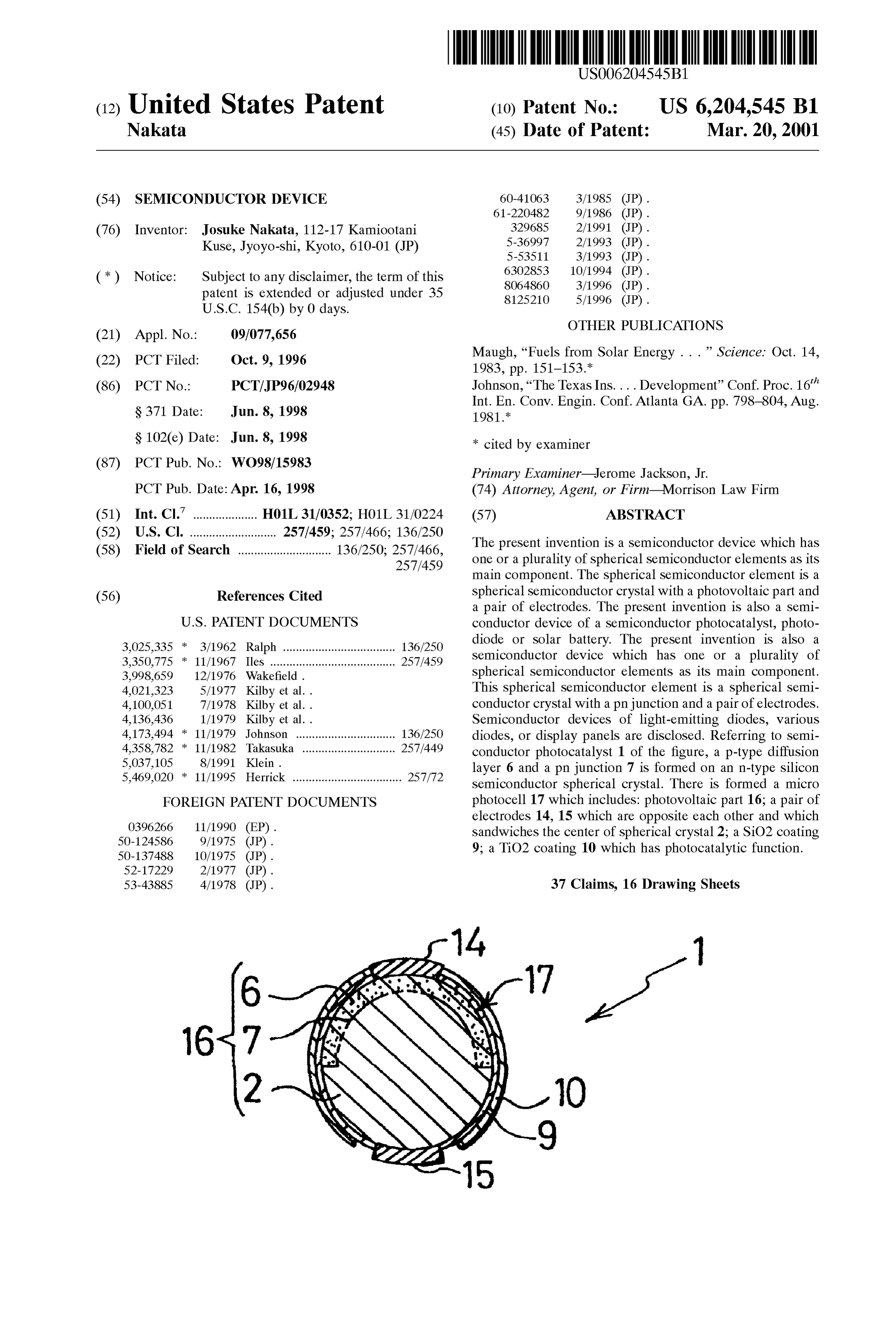
S 102(e) Date: Jun. 8, 1998 * cited by examiner (87) PCT Pub. No.: WO98/15983 Primary Examiner Jerome Jackson, Jr. PCT Pub. Date: Apr. 16, 1998 (74) Attorney, Agent, or Firm Morrison Law Firm (51) Int. Cl." .................... H01L 31/0352; H01L 31/0224 (57) ABSTRACT (52) U.S. Cl. ........................... 257/459; 257/466; 136/250 The present invention is a Semiconductor device which has (58) Field of Search ............................. 136/250; 257/466, one or a plurality of Spherical Semiconductor elements as its
main component. The Spherical Semiconductor element is a (56) References Cited Spherical Semiconductor crystal with a photovoltaic part and a pair of electrodes. The present invention is also a Semi
3,025,335 * 3/1962 Ralph ... ... 136/250 diode or Solar battery. The present invention is also a 3,350,775 11/1967 Iles ....................................... 257/459 Semiconductor device which has one or a plurality of 3,998.659 12/1976 Wakefield. Spherical Semiconductor elements as its main component. 4,021,323 5/1977 Kilby et al.. This spherical Semiconductor element is a spherical Semi 4,100,051 7/1978 Kilby et al.. conductor crystal with a pnjunction and a pair of electrodes. 4,136,436 1/1979 Kilby et al.. Semiconductor devices of light-emitting diodes, various 4,173,494 * 11/1979 Johnson ............................... 136/250 diodes, or display panels are disclosed. Referring to Semi 4,358,782 11/1982 Takasuka ............................. 257/449 conductor photocatalyst 1 of the figure, a p-type diffusion 5,037,105 8/1991 Klein. layer 6 and a pn junction 7 is formed on an n-type Silicon 5,469,020 11/1995 Herrick .................................. 257/72 Semiconductor Spherical crystal. There is formed a micro FOREIGN PATENT DOCUMENTS photocell 17 which includes: photovoltaic part 16; a pair of
electrodes 14, 15 which are opposite each other and which
Sandwiches the center of spherical crystal 2, a SiO2 coating 50-137488 10/1975 (JP). 9; a TiO2 coating 10 which has photocatalytic function.
53-43885 4/1978 (JP). 37 Claims, 16 Drawing Sheets
Page 2
Drawing sheet — no readable text.
Page 3
Drawing sheet — no readable text.
Page 4
Drawing sheet — no readable text.
Page 5
Drawing sheet — no readable text.
Page 6
Drawing sheet — no readable text.
Page 7
Drawing sheet — no readable text.
Page 8
Drawing sheet — no readable text.
Page 9
Drawing sheet — no readable text.
Page 10
Drawing sheet — no readable text.
Page 11
Drawing sheet — no readable text.
Page 12
Drawing sheet — no readable text.
Page 13
Drawing sheet — no readable text.
Page 14
Drawing sheet — no readable text.
Page 15
Drawing sheet — no readable text.
Page 16
Drawing sheet — no readable text.
Page 17
Drawing sheet — no readable text.
Page 18
SEMCONDUCTOR DEVICE Furthermore, because there is a volume increase when molten Silicon Solution Solidifies, and because Solidification
TECHNICAL FIELD begins from the surface, the part which solidifies last will The present invention relates to a Semiconductor device, protrude towards the Surface of the Spherical crystal, and a comprising: bead-like, Spherical Semiconductor elements protruding area is formed. A truly Spherical sphere crystal is which incorporate a pn-junction into a spherical crystal of a not formed. However, with the drop tube type experimental Semiconductor and which have a pair of electrodes. The apparatus of NASA, because it is equipped with an electro present invention further relates to a Semiconductor device magnetic levitation heating equipment, the material is allowed to melt and free fall.
which can be used in Semiconductor photocatalysts, Solar batteries, display panels, or other various applications. In this USP, a pn junction is formed on the spherical crystal of Silicon. There is also disclosed a Solar cell array
BACKGROUND TECHNOLOGY where there is formed a metal electrode film which is Semiconductor photocatalysts receive light from Sunlight common to a plurality of these sphere crystals (micro or the like and generate photovoltage. An electrochemical 15 photocells). Furthermore, these Solar cell arrays are Sub reaction is triggered by this photovoltage. Metal oxide merged in electrolyte Solution. There is also disclosed a Semiconductors of titanium oxide (TiO2), Strontium titanate photochemical energy conversion device where electrolysis (SrTiO2), or the like have been utilized as semiconductor proceeds by theofphotovoltage of a solution hydroiodic acid and hydrobromic acid provided by Sunlight.
photocatalysts. Titanium oxide is used as an electrode of a photochemical battery. A platinum electrode and a titanium In the silicon Solar cell array of this USP, there is not a pair oxide electrode are placed in water. When light is Shined on of electrodes formed for each individual micro photocell, the titanium oxide electrode, electrolysis of water is known but there is a common electrode formed for a plurality of to occur. Furthermore, there has been research on photo micro photocells. It is not possible to handle individual catalysts in which metals. Such as platinum are Supported by micro photocells independently. As a result, the micro a powder of a metal oxide Semiconductor as well as research 25 photocells can not be dispersed in the electrolyte Solution as on electrodes comprising a thin film of titanium oxide on one individual Semiconductor photocatalysts. Their installation Side of a titanium plate. positions can not be changed, nor can they be recovered and When using a titanium oxide photocatalyst for the elec reused or washed. The limitations in its use as a Semicon trolysis of water by Sunlight, only the portion of the Spec ductor photocatalyst are extremely large. In addition, in this trum which is approximately 410 nm or lower can be used USP, there is no disclosure regarding the use of Semicon from the entire light spectrum of Sunlight. As a result, the ductors with photocatalytic capability as electrodes, nor is photoelectric conversion efficiency is extremely low. The there disclosure regarding the use of Semiconductors which following are conditions which are necessary for a Semi have photocatalytic function and which are Selected by conductor photocatalyst or Semiconductor electrode to be considering the reaction activity or reaction selectivity. able to electrolyze water and for it to be able to adequately 35 Because there is not a pair of electrodes on the Surface of utilize the Spectrum of Sunlight: a photovoltage greater than each of the microphotocells described above, a Single or a or equal to the electrolytic voltage of water (theoretical plurality of Spherical Semiconductor elements having a pn value 1.23 V); a chemical stability so that there is no junction can not be incorporated into a Semiconductor photodissociation of the Semiconductor photocatalyst in the device in Such a way that they are independent cells or electrolyte Solution, and the like. 40 elements. Because the mode of electrical connection of the
Because the energy band gap of metal oxide Semiconduc plurality of spherical Semiconductor elements is fixed, it tors of titanium oxide or the like is large, it has the lackS in generalizability and is not practical. advantages of the electrolysis of water being possible and of In the prior art, a color display has been put into practical not dissolving in the electrolyte Solution. However, there is use. This color display incorporates a plurality of light a problem because it does not function as a photocatalyst 45 emitting diodes which are of three types, emitting red light, with the light spectrum when the wavelength is longer than blue light, or green light. Because each of the light emitting approximately 410 nm. As a result, when conducting chemi diode lamps can not have a detailed construction, it is not cal reactions using Sunlight for the photocatalytic action, appropriate for Small or light weight high resolution dis only a Small portion of the light spectrum of Sunlight can be playS. In the case of a large size display, the number of parts used, and the energy conversion efficiency becomes 50 is large, and it does not have an overall Simple construction. extremely poor. In order to increase catalytic efficiency, the The assembling cost is high. Using an integrated circuit photocatalyst of titanium oxide or the like is used in the form technology, it is possible to produce light emitting diode of a fine powder. However, this flows easily in the electro elements which emit 3 colors of light, but the production lyte Solution, and as a result, recovery for the purpose of costs become expensive. The interior integrated circuit reuse is difficult. With regard to a photocatalyst in which a 55 becomes complicated, and defective products are more metal of platinum or the like is Supported by a titanium oxide easily generated. This is not practical. powder, because the anode site (site of oxidation reaction) The object of the present invention is to provide the and the cathode site (site of reduction reaction) exist close to following: a Semiconductor device with a spherical Semi each other, the probability of the reverse reaction is large. conductor element which is bead-like, has photovoltaic This is not very practical. 60 capability, and has a pair of electrodes, a Semiconductor In U.S. Pat. No. 4,021,323, there is described a photocatalyst which has excellent photoelectric conversion technology, wherein: Small amounts of molten Silicon Solu efficiency and which is practical and generalizable; a Semi tion are sprayed from a Small nozzle which is placed on the conductor photocatalyst with an increased electric potential upper end of a shot tower; Silicon Solution is allowed to free between the oxidizing and reducing electrodes, a Semicon fall, and Spherical crystals of Silicon are created. However, 65 ductor photocatalyst in which the electric potential between with this technology, there is the possibility of impurities the oxidizing and reducing electrodes can be adjusted freely; dissolving into the molten Silicon Solution from the nozzle. a Semiconductor device as a Solar battery which can receive
Page 19
incident light over a broad range and which has a high in a single row and a Serial electrical connection can be utilization efficiency of the Semiconductor material; a Semi created Simply by connecting electrodes with opposing conductor device as a Solar battery which has a high degree polarities. The connection can be maintained by the photo of freedom in its electrical connections and which has a thin Voltage. For the Serial connection, the Serial connection can thickness, various Semiconductor devices or the like as be made easily by applying an external electric field while photodiodes. Shining a light.
A further object of the present invention is to provide the The photovoltaic part comprises a diffusion layer which is following: a Semiconductor device with a spherical Semi formed near the Surface of the Spherical crystal and a pn conductor element which is bead-like, has light emitting junction (claim 3 which is dependent on claim 2). If the capability through a pnjunction, and has a pair of electrodes, Spherical crystal is a p-type Semiconductor, there is a n-type a Semiconductor device as a light emitting element which diffusion layer, if the Spherical crystal is a n-type can emit light over a broad range and which has a high Semiconductor, there is a p-type diffusion layer. The photo utilization efficiency of the Semiconductor material; a Semi Voltage is generated via the pn junction which is at the conductor device as a light emitting element which has a border between the diffusion layer and the semiconductor high degree of freedom in its electrical connections and 15 crystal which forms the Spherical crystal. As a result, the which has a thin thickness, Semiconductor devices or the Voltage is high and has excellent Stability. It is advantageous like as light emitting diodes, display panel, or various in terms of the photoelectric conversion efficiency. diodes. The photovoltaic part has an MIS configuration where an
DISCLOSURE OF THE INVENTION
insulating coating is formed on a portion of the Surface of the
Spherical crystal, and a metal coating, which Serves as an
The Semiconductor device of the present invention com electrode of one polarity, is formed on the Surface of this prises: Spherical Semiconductor elements which are granular insulating coating (claim 4 which is dependent on claim 2). and independent and comprising: a spherical crystal of MIS is an abbreviation for Metal Insulator Semiconductor. p-type Semiconductor or n-type Semiconductor; a photovol 25 The MIS configuration is a known art. The configuration of taic part which is incorporated onto the Surface or onto an the photovoltaic part is simplified, and this is advantageous area near the Surface of the Spherical crystal and which in terms of manufacturing costs.
generates photovoltage in association with the Spherical The photovoltaic part has a Schottky barrier configuration crystal; at least one pair of electrodes which is on both sides where a metal coating is formed on a portion of the Surface of the photovoltaic part and is also on the Surface of the of the Spherical crystal, and this metal coating Serves as an spherical crystal and which is mutually separated (claim 1). electrode of one polarity (claim 5 which is dependent on When light is shined on the spherical semiconductor claim 2). The Schottky barrier construction is a known art. element, the photovoltage which is generated in the photo The construction of the photovoltaic part can be made Voltaic part appears on the pair of electrodes. A potential extremely simple. This is advantageous in terms of the difference is generated between the pair of electrodes. This 35 manufacturing costs.
Semiconductor device can be constructed from a single or a The Spherical Semiconductor element is a Semiconductor plurality of spherical Semiconductor elements. It can also photocatalyst, which, with the photovoltage generated when have other compositional elements as well. When this semi the photovoltaic part receives light, generates an electro conductor device is immersed in an electrolyte Solution, chemical reaction between the electrodes and the electrolyte current flows from the positive electrode to the negative 40 Solution. (claim 6 which is dependent on one of the claims electrode, passing through the electrolyte Solution. AS a of claims 3-5).
result, there is an oxidizing action in which electrons are Examples of the electrochemical reaction include the absorbed at the positive electrode, and there is generated a electrolysis of water, electrolysis of methanol aqueous reducing action at the negative electrode where electrons are Solution, electrolysis of hydriodic acid Solution, or the given up. There is an electrochemical reaction correspond 45 electrolysis of various other electrolyte solutions. In this ing to the electrolyte Solution. In the case where the Semi case, the Semiconductor device can be constructed Solely conductor device is maintained in atmospheric conditions or from a plurality of spherical Semiconductor elements. Mate in a vacuum, when light is Shined on the Spherical Semi rial with a catalytic function is preferred for the material of conductor element, a potential difference is generated the electrode. Using reaction activity and reaction Selectivity between the electrodes. Light energy is converted to elec 50 as a basis, material which is to be used for the electrode is trical energy. As a result, this can be used in Solar batteries Selected on its relation with the reaction products. For or photodiodes. example, for a hydrogen generating reducing electrode, Ni Because the Spherical Semiconductor element has a pair of (nickel), Ru (ruthenium), Ir (iridium), or their oxides are electrodes and is constructed as independent particles, this is preferred, but it is not limited to these. Appropriate material advantageous for lining up a plurality of Spherical Semicon 55 for a reducing electrode which generates methane is Pd ductor elements and for connecting them electrically. When (palladium), Rh(rhodium), but is not limited to these. When creating a Semiconductor device by incorporating a single or an electrode of one polarity is constructed with a metal oxide a plurality of spherical Semiconductor elements to other Semiconductor which functions as a photocatalyst, the acti compositional elements, there is a high degree of freedom, Vating Voltage for the electrochemical reaction can be low, and it has excellent generalizability. The Strength of the 60 and the energy conversion efficiency is increased. generated Voltage can also be chosen freely. The Semiconductor device comprises a plurality of spheri The electrode with one polarity and the electrode with the cal Semiconductor elements. The Semiconductor device is other polarity are placed So that they are at least partially operated while Several spherical Semiconductor elements at opposite each other with the center of the Spherical crystal a time are connected electrically in Series via the photovolt interposed between them (claim 2 which is dependent on 65 age generated by the photovoltaic part of the Spherical claim 1). When the electrodes are constructed in this way, a Semiconductor elements which are in the electrolyte Solution plurality of spherical Semiconductor elements can be aligned (claim 7 which is dependent on claim 6). In this case, the
Page 20
S 6
Semiconductor device does not require compositional ele The spherical crystal described above is constructed from ments other than a plurality of Spherical Semiconductor a semiconductor of Si or SiGe, Group III-V compound elements. The plurality of bead-like Spherical Semiconductor Semiconductor of GaAS or InP or the like, chalcopyrite-type elements can be used as Semiconductor photocatalysts. semiconductor of CuInSe2 or the like (claim 12 which is Depending on the type of electrochemical reaction, the dependent on one claim from claims 3-5).
Spherical Semiconductor elements can be used each The Semiconductor device comprises: a transparent case independently, or n of these (n an integer of 2 or greater) can which has a storage cavity which Stores a single Spherical be connected in Series, and a photovoltage of approximately Semiconductor element; a pair of external electrodes which n times can be generated. In this case, the plurality of is partially inserted into both sides of the Storage cavity and Spherical Semiconductor elements can be dispersed in the 1O hermetically Seals the cavity; the pair of external electrodes electrolyte Solution; the placement positions can be changed being electrically connected to electrodes of each of the as appropriate; recovery and reuse is possible. As a result, spherical Semiconductor elements (claim 13 which is depen there is a the degree of freedom in its usage, and there is dent on one claim from claims 3-5). This semiconductor excellent generalizability. Because the positive electrode device is appropriate for photodiodes. When light is Shined and the negative electrode are separated, the reverse reaction from outside of the case, a potential difference is generated is prevented. Because the Spherical Semiconductor can be 15 in the pair of external electrodes. Because the Spherical illuminated from a light from broad range of incident angles, Semiconductor element is housed inside a transparent case, it is advantageous when using Sunlight. Furthermore, Spheri it is possible to detect incident light from the entire 360 cal Semiconductor elements have excellent mechanical degree range.
Strength. The Semiconductor device comprises: a Semiconductor The Surface of the Spherical crystal, other than at the element array in which a plurality of the Spherical Semicon electrodes, is covered with an insulating coating which is ductor elements is electrically connected in Series and is light transparent and has anti-reflective properties (claim 8 lined up in a Single row, a transparent case which has a which is dependent on claim 6). This insulating coating can Storage cavity which Stores this Semiconductor element be a coating of one layer, or it can be a coating of 2 layers. array; a pair of external electrodes which is partially inserted Electrical and chemical Stability is maintained by the insu 25 onto both Sides of the Storage cavity of the case and lating action of the insulating coating. The rate of reflection hermetically Seals it; the pair of electrodes being electrically of light is lowered due to the anti-reflective function of the connected to each of the electrodes of the Spherical Semi insulating coating, and the efficiency is improved. The conductor elements which are on both ends of the Semicon following materials can be used as material for the insulating ductor array (claim 14 which is dependent on one claim from coating: SiO2, Si3N4, Al2O3, Ta2O5, TiO2, MgF2, SnO2, claims 3-5). This semiconductor device is suitable for or Nb2O5, or the like. However, the material for the insu photodiode arrays or Solar cell arrayS. Because the Semi lating coating is to be Selected in relation with the Spherical conductor element array is housed inside a transparent case, crystal material. it is possible to detect incident light from the entire 360 The Surface of the insulating coating is covered with a degree range. By adjusting the number of Spherical Semi light transparent coating which is connected to an electrode 35 conductor elements which are connected in Series, the size of one polarity; this coating is made of metal oxide Semi of photovoltage can be adjusted appropriately. conductor which has a photocatalytic capacity (claim 9 In the casing described above, a plurality of Storage which is dependent on claim 8). The electrochemical reac cavities can be formed in parallel; a Semiconductor element tion can be accelerated by the photocatalytic capacity of this array is placed in each Storage cavity; a pair of external coating. Metal oxide Semiconductors which have a photo 40 electrodes is placed on either end of each Storage cavity catalytic capacity include: TiO2, SrTiO3, Fe2O3, PbxTi(1- (claim 15 which is dependent on claim 14). The overall X)O2, and the like. The energy band gap curves at the phase Semiconductor device is panel-like or sheet-like. It receives boundary Surface where these metal oxide Semiconductors incident light from either Side of the transparent case and are in contact with the electrolyte solution. The hole and the converts it to Voltage. The multi-row multi-column Spherical electrons Separate, and the oxidation reaction or reduction 45 Semiconductor elements can reliably receive incident light reaction is accelerated. even when there are large changes in the angle of incidence The Surface of an electrode of one polarity and a portion of the light. It is Suited for Solar battery panels. Furthermore, or the entire Surface of the insulating coating is covered with because a portion of the incident light exits from the a light transparent electrode coating; this coating is made of opposite Side by passing through the Spherical Semiconduc metal oxide Semiconductor which has a photocatalytic 50 tor elements and the case, it can be a Solar battery panel capacity (claim 10 which is dependent on claim 8). This which also serves as window glass.
electrode coating can accelerate the electrochemical reaction The Semiconductor device comprises: a Semiconductor by its photocatalytic capacity. Furthermore, the electric element array in which a plurality of the Spherical Semicon potential between the oxidizing and reducing electrodes can ductor elements is electrically connected in Series and is be increased. 55 lined up in a single row, a pair of electrodes being electri The electrode of one polarity is constructed from a cally connected to each of the electrodes of the Spherical light-transparent electrode coating; this coating is formed on Semiconductor elements which are on both ends of the the Surface of the diffusion layer and forms a hetero-junction Semiconductor array; a transparent case member which with respect to the diffusion layer; this electrode coating is covers the exterior of the Semiconductor element array made of metal oxide Semiconductor which has a photocata 60 (claim 16 which is dependent on one of the claims of claims lytic capacity. (claim 11 which is dependent on claim 8). The 3-5). The case member is preferably constructed from a barrier for the carrier is reduced by the hetero-junction. In Synthetic resin material of Silicone resin or the like. The addition, the photovoltaic effect of the pnjunction, which is Semiconductor element array can be imbedded inside the created by the diffusion layer which is formed near the case member. All other aspects are the same as the Semi Surface of the Spherical crystal, and the metal oxide 65 conductor device in claim 13.
Semiconductor, which has a photovoltaic capacity, act in A plurality of the Semiconductor element array can be cooperation to increase the photocatalytic effect. placed in parallel; the plurality of Semiconductor element
Page 21
arrays are Stored in an imbedded State inside the case Semiconductor element; a pair of external electrodes which member; a plurality of pairs of electrodes are placed corre is partially inserted onto both ends of the Storage cavity and sponding to the plurality of Semiconductor element arrayS which hermetically Seals it; the pair of external electrodes (claim 17 which is dependent on claim 16). The case being connected electrically to the electrodes of each of the member is preferably constructed from a Synthetic resin spherical Semiconductor elements (claim 21 which is depen material of Silicone resin or the like. Because the Semicon dent on claim 20). This semiconductor device is suited for ductor element arrays are imbedded inside the case member, rectifier diodes and variable capacity diodes or the like. the incidence efficiency of the light is heightened. Other Voltage can be applied to the pair of electrodes of the aspects are the Same as in the Semiconductor device of claim Spherical Semiconductor element via the pair of external 15. 1O electrodes.
A Semiconductor device comprises: Spherical Semicon A Semiconductor device comprises: a Semiconductor ele ductor elements which are independent and bead-like, com ment array in which a plurality of the Spherical Semicon prising: a spherical crystal of p type Semiconductor or n-type ductor elements is electrically connected in Series and is Semiconductor; a diffusion layer and a pn junction formed lined up in a Single row, a transparent case which has a near the Surface of the Spherical crystal; at least one pair of 15 Storage cavity which Stores this Semiconductor element electrodes which is on both Sides of the pn junction and is array; a pair of external electrodes which is partially inserted also on the Surface of the Spherical crystal and which is onto both Sides of the Storage cavity of the case and mutually separated (claim 18). When voltage is applied to hermetically Seals it; the pair of electrodes being electrically the pair of electrodes of the Spherical Semiconductor connected to each of the electrodes of the Spherical Semi element, the Semiconductor device emits light at the pn conductor elements which are on both ends of the Semicon junction as a function of the type of Semiconductor Spherical ductor array (claim 22 which is dependent on claim 20). crystal and the type of dopants contained in the Semicon When Voltage is applied to the pair of external electrodes, a ductor. This principle of the light emission is the same as the plurality of Spherical Semiconductor elements of the Semi principle for known light emitting diodes. The configuration conductor element array emit light Therefore, this Semicon of the light emitting mechanism is the Same as in known 25 ductor device is Suitable for light emitting diode arrayS. light emitting diodes. Because the Semiconductor element array is housed inside a AS a result, this Semiconductor device is Suited as a light transparent case, light can exit from the entire 360 degree emitting element. However, it can also be used for various range. By adjusting the number of Spherical Semiconductor diodes or the like Such as other rectifier diodes or the like. elements which are connected in Series, the light emitting The type of Semiconductor, the type of doping agent capacity can be adjusted appropriately.
elements, the type of pn junction (in other words, the In the casing described above, a plurality of Storage configuration of the spherical Semiconductor element) can cavities can be formed in parallel; a Semiconductor element be set for the desired light emitting function or other array is placed in each storage cavity; a pair of external function. The Settings are based on known technology electrodes is placed on either end of each Storage cavity relating to light emitting diodes. The Semiconductor device 35 (claim 23 which is dependent on claim 22). The overall can be constructed from a Single or a plurality of Spherical Semiconductor device is panel-like or sheet-like. Although Semiconductor elements, and can also include other con light exits from either Side of the transparent case, light can figuration elements. When using as a light emitting element, be made to exit from only one Side by forming a reflective because light is emitted in the interior of the Spherical coating on the other side. When light is emitted from a Semiconductor element, there are no limitations on the 40 plurality of rows and a plurality of columns of the Spherical direction in which the light exits, and light can exit in all Semiconductor elements, it becomes a light emitting Surface. directions. The Spherical Semiconductor element has a pair It is Suited for a light emitting Surface device. of electrodes and is constructed as independent particles. AS A Semiconductor device comprises: a Semiconductor ele a result, this is advantageous for connecting resistance wires ment array in which a plurality of the Spherical Semicon individually to each spherical semiconductor element. When 45 ductor elements is electrically connected in Series and is making a Semiconductor device which incorporates a Single lined up in a Single row, a pair of electrodes which is or a plurality of Spherical Semiconductor elements to other electrically connected to each of the electrodes of the configuration elements, there is a high degree of freedom Spherical Semiconductor elements which are on both ends of and excellent generalizability. The light emitting capability the Semiconductor array; a transparent case member which can also be set freely. 50 covers the exterior of the Semiconductor element array The Surface of the Spherical crystal, other than at the (claim 24 which is a dependent of claim 20). The case electrodes, is covered with an insulating coating which is member is preferably constructed from a Synthetic resin light transparent (claim 19 which is dependent on claim 18). material of Silicone resin or the like. The Semiconductor The insulating coating can be a Single layer coating, or a 2 element array can be imbedded inside the case member. layer coating. Electrical and chemical Stability can be main 55 Other aspects are the same as in the Semiconductor device of tained by the insulating action of the insulating layer. The claim 22.
electrode with one polarity and the electrode with the other There are a plurality of rows of Semiconductor element polarity are placed So that they are at least partially opposite arrays; this plurality of Semiconductor element arrays are each other with the center of the Spherical crystal interposed embedded in the transparent sheet-like case member between them (claim 20 which is dependent on claim 19). 60 described above; there are a plurality of pairs of electrodes When the electrodes are constructed in this way, a plurality which correspond to the plurality of Semiconductor element of Spherical Semiconductor elements can be lined up in a arrays (claim 25 which is dependent on claim 24). The case Single row. They can be electrically connected in a Serial member is preferably constructed from a Synthetic resin manner Simply by having electrodes of different polarities in material of Silicone resin or the like. Because the Semicon contact with each other. 65 ductor element array is imbedded inside the case member, A Semiconductor device comprises: a transparent case the light exiting efficiency is heightened. Other aspects are which has a Storage cavity which Stores one Spherical the same as in the Semiconductor device of claim 23.
Page 22
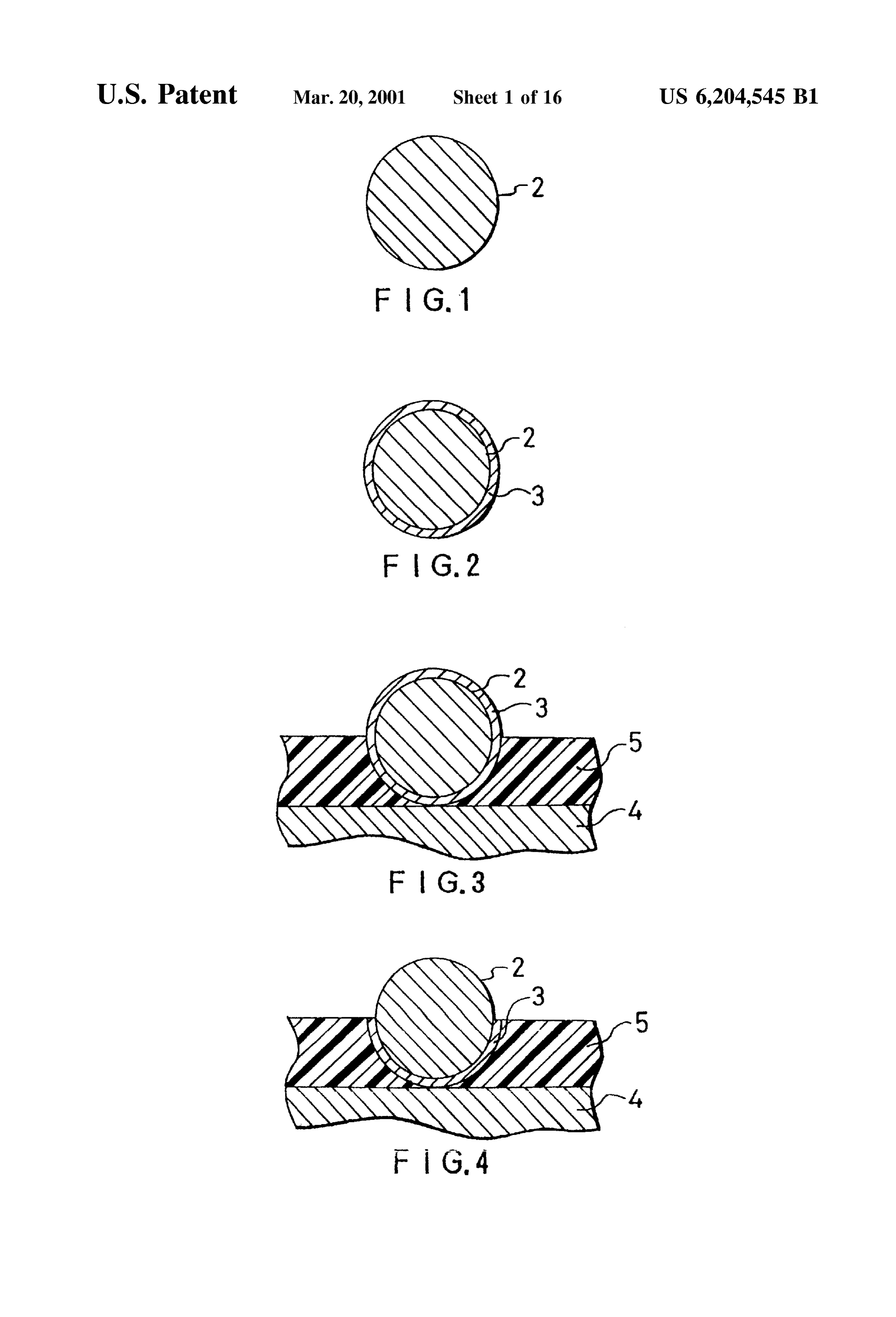
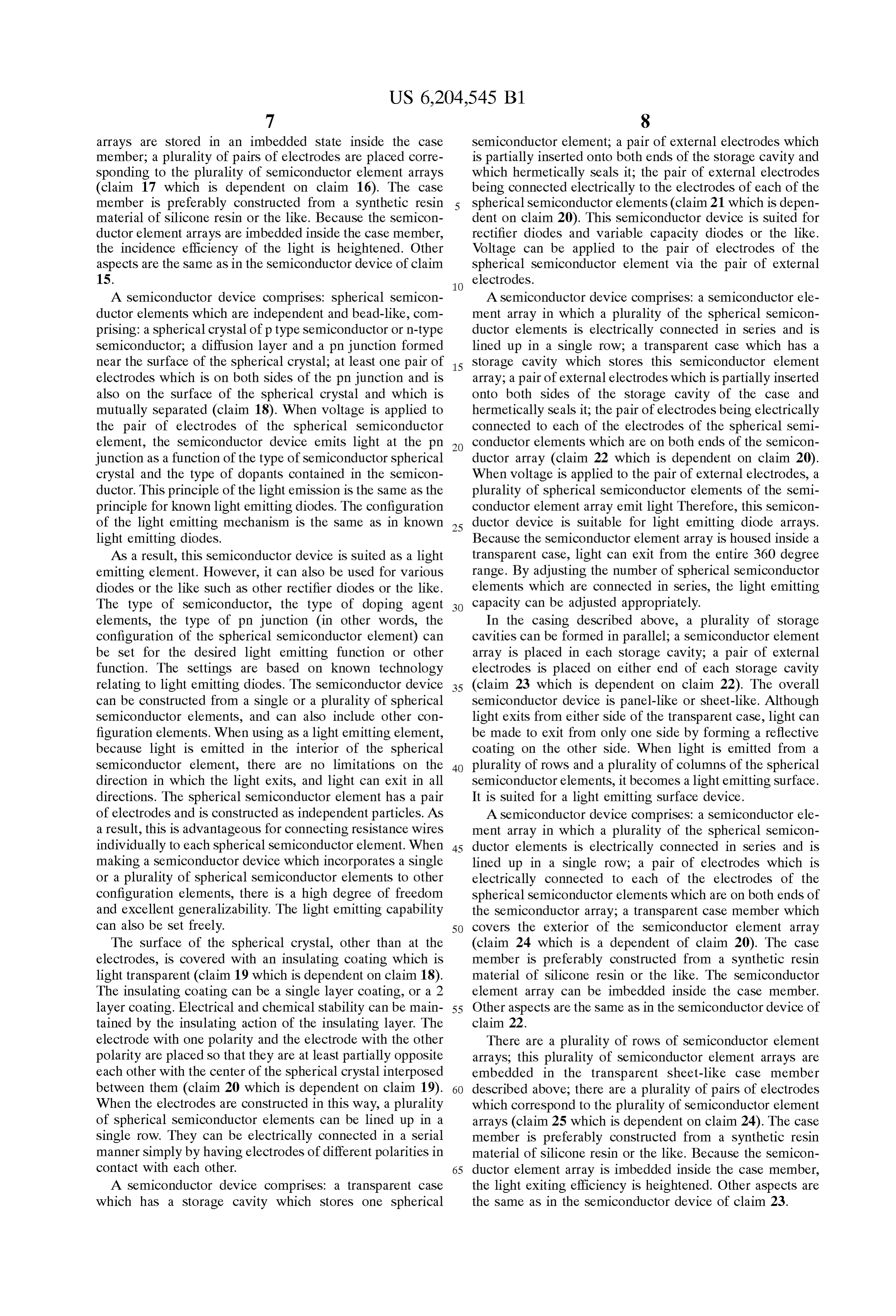
The present Semiconductor device is a device which has FIG. 1 is a cross-sectional diagram of a spherical crystal a light emitting function in which light is emitted by of a Semiconductor.
applying Voltage to the Spherical Semiconductor elements FIG. 2 is a cross-sectional diagram of the Spherical crystal (claim 26 which is dependent upon one of the claims of covered with a coating.
FIG. 3 is a cross-sectional diagram in which the Spherical
The Semiconductor device is a device which functions as crystal is covered with a coating and masked with a resin a light emitting display panel, wherein: a plurality of the film.
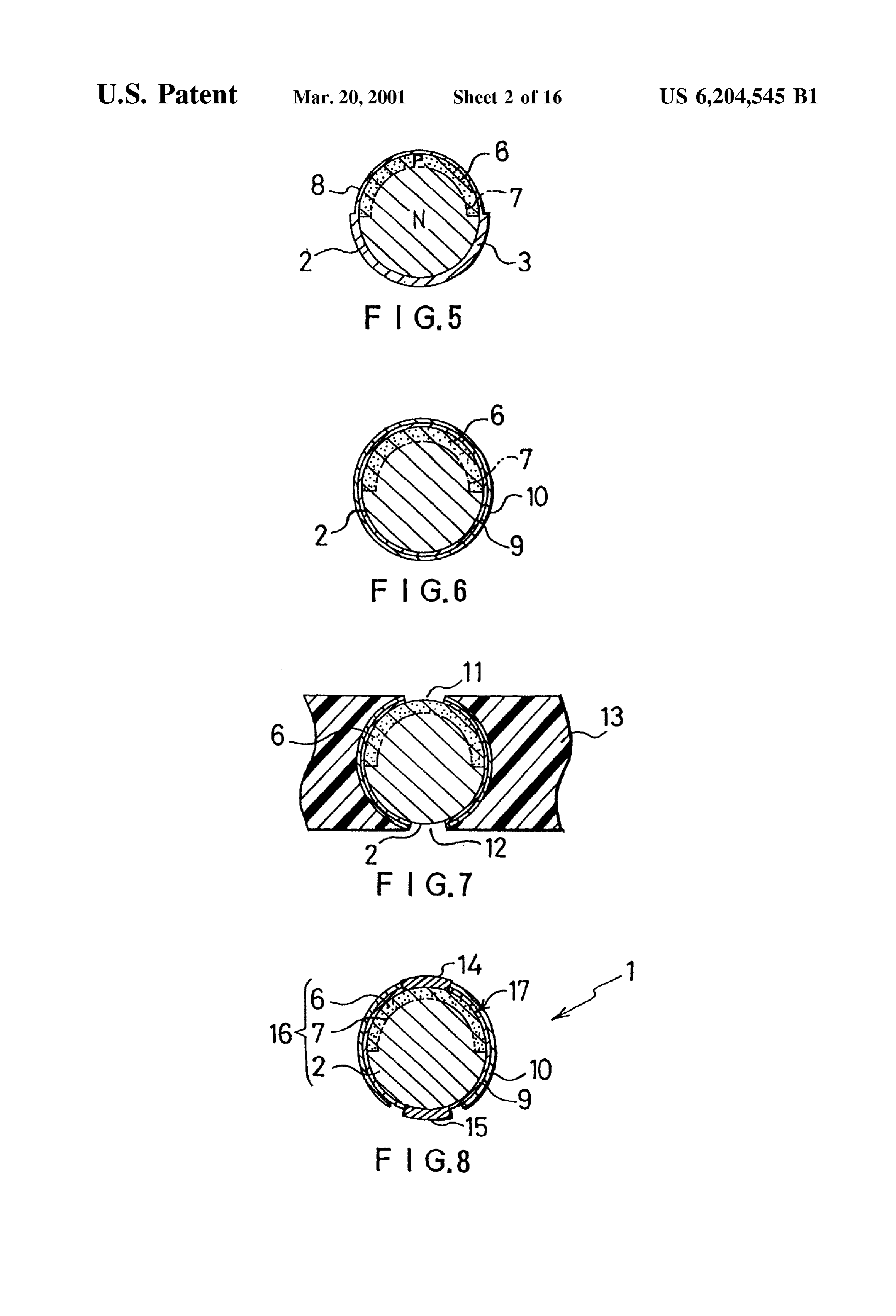
Spherical Semiconductor elements are placed to make a FIG. 4 is a cross-sectional diagram in which etching has matrix of a plurality of rows and a plurality of columns, been done after masking.
these plurality of spherical Semiconductor elements are FIG. 5 is a cross-sectional diagram in which a p-type housed in a case member which is transparent and panel diffusion layer is formed on the Spherical crystal. like, light is emitted by Selectively applying Voltage to the pair of electrodes of each individual Semiconductor ele FIG. 6 is a cross-sectional diagram in which there is a ments. (claim 27 which is dependent upon claim 18). The 15 coating formed on the Surface of the Spherical crystal. overall Semiconductor device is panel-like. Although light FIG. 7 is a cross-sectional diagram in which there is a exits from both sides of the transparent case, light can be light Sensitive resin film mask, and an opening is formed. made to exit from only one side by forming a reflective FIG. 8 is a cross-sectional diagram of a Semiconductor coating on the other side. In the case of a large Size display photocatalyst.
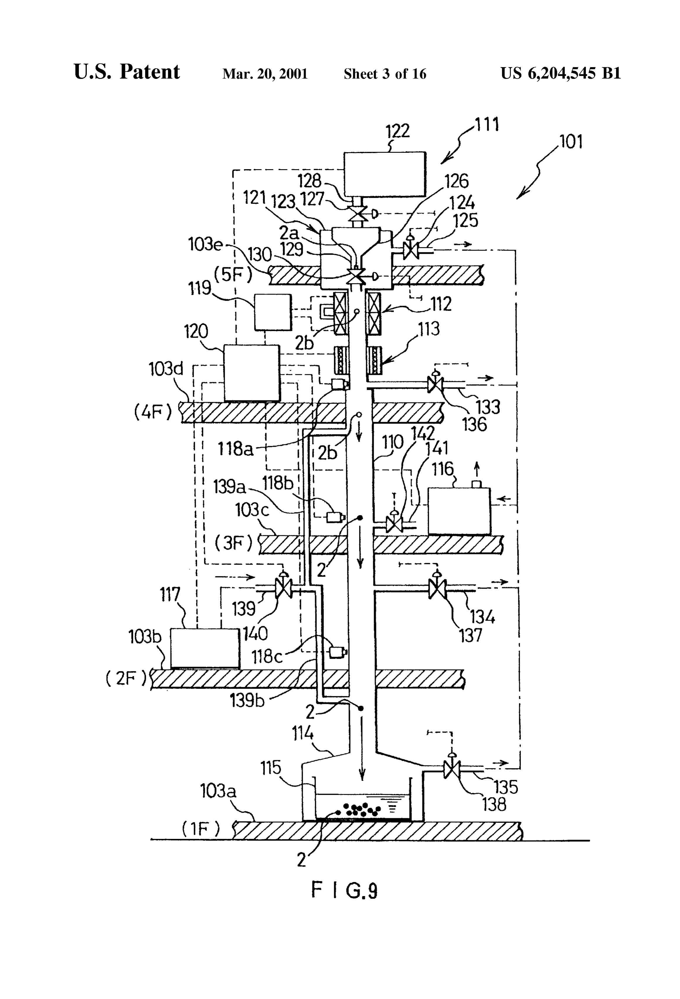
panel, the diameter of the Spherical Semiconductor element FIG. 9 is a block diagram of a semiconductor spherical can be of a Size of Several mm, but in the case of a Small size crystal manufacturing device.
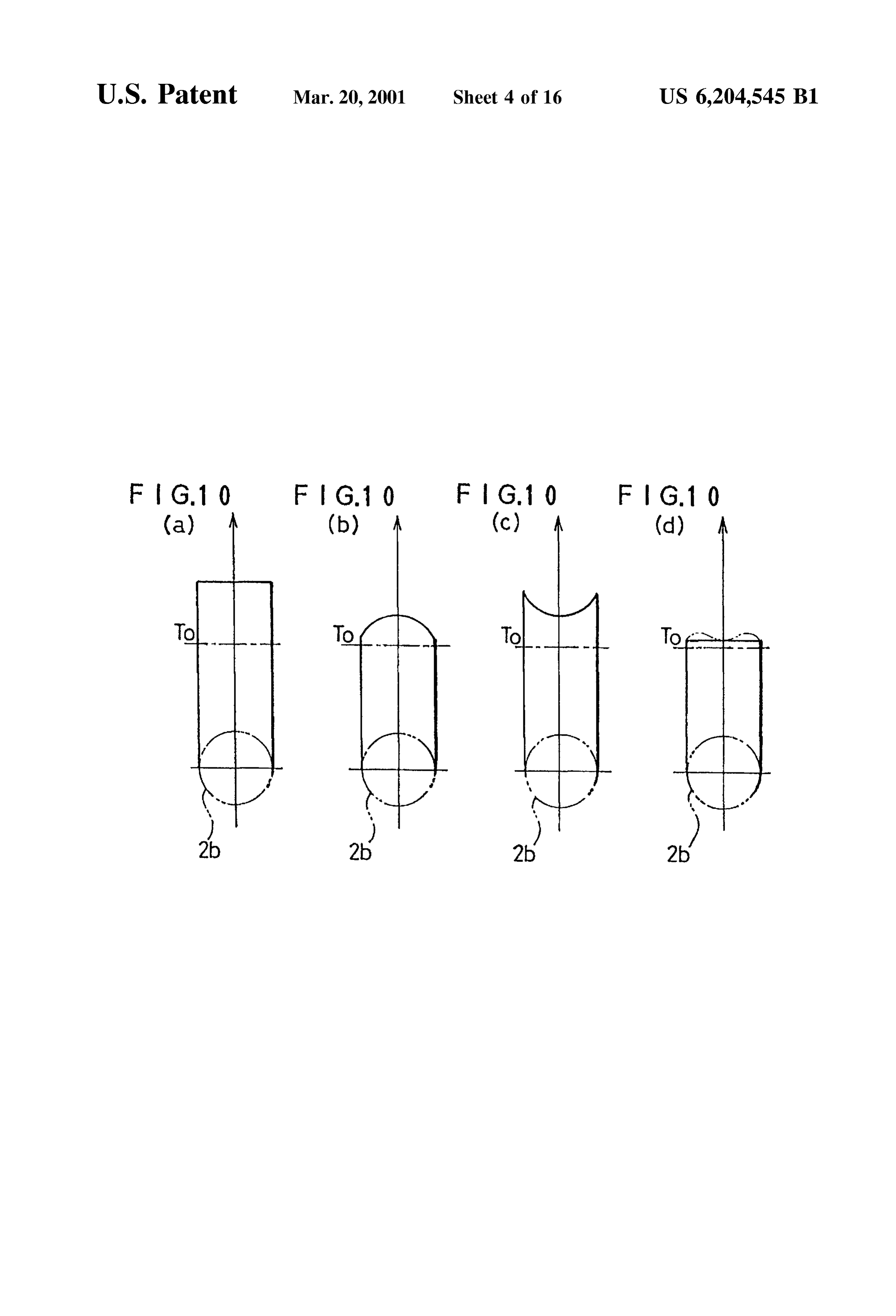
display panel on the order of a CRT display or a liquid crystal display, the diameter of the Spherical Semiconductor moltenFIG. 10(a) is a temperature distribution diagram of a element is on the order of 200-300 micrometer. Solution immediately after melting. Furthermore, in order to prevent the light leaving each FIG. 10(b) is a temperature distribution diagram of the Spherical Semiconductor element from leaking towards 25 molten Solution immediately after the commencement of neighboring Spherical Semiconductor elements, it is prefer dropping.
able to form a fine Separating wall which optically isolates FIG. 10(c) is a temperature distribution diagram of the the Spherical Semiconductor elements. molten Solution immediately after heating with an infrared In the case of a monochromatic display panel, one type of heater.
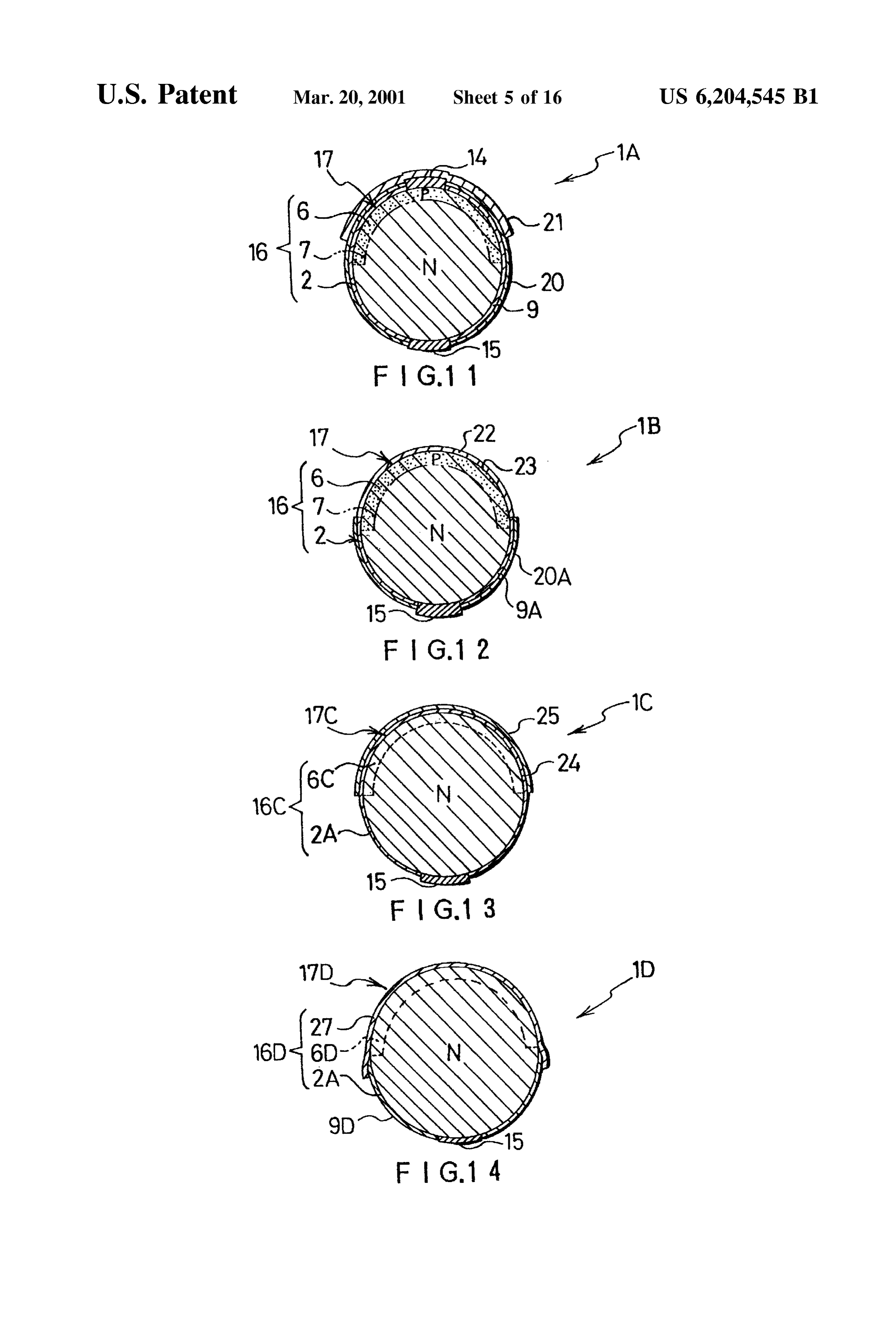
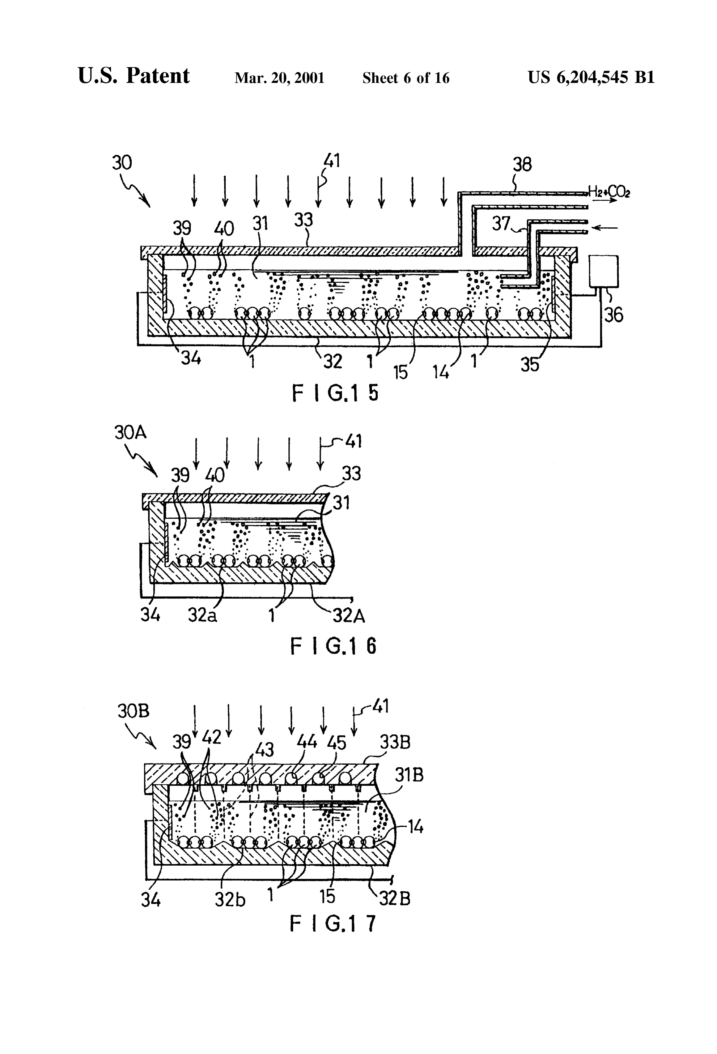
Spherical Semiconductor element is used. In the case of a FIG. 10(d) is a temperature distribution diagram of the color display panel, it is necessary to generate full color light molten Solution immediately after Solidification has begun. by the Synthesis of the three colors of red, green, and blue FIG. 11 is a cross-sectional diagram of a modification light. As a result, the plurality of spherical Semiconductor mode 1 of the Semiconductor photocatalyst. elements comprises: a plurality of spherical Semiconductor 35 FIG. 12 is a croSS-Sectional diagram of a modification elements number 1 which is capable of generating red light; mode 2 of the Semiconductor photocatalyst. a plurality of spherical Semiconductor elements number 2 which is capable of generating green light; a plurality of FIG. 13 is a croSS-Sectional diagram of a modification Spherical Semiconductor elements number 3 which is mode 3 of the Semiconductor photocatalyst.
capable of generating blue light. Spherical Semiconductor 40 FIG. 14 is a croSS-Sectional diagram of a modification elements numbers 1-3 are alternated cyclically in the row mode 4 of the Semiconductor photocatalyst. direction of the matrix, and are alternated cyclically in the FIG. 15 is a cross-sectional diagram of an electrolytic column direction of the matrix (claim 28 which is dependent device with a Semiconductor photocatalyst. upon claim 27). FIG. 16 is a Schematic cross-sectional diagram of an Each spherical crystal in the Spherical Semiconductor 45 electrolytic device with a Semiconductor photocatalyst elements numbers 1-3 are n-type GaAS Semiconductors. which has been partially modified.
The diffusion layer on the Spherical crystal contains Zn as FIG. 17 is a Schematic cross-sectional diagram of an the p-type dopant (claim 29 which is dependent upon claim electrolytic device with a Semiconductor photocatalyst 28). On the surface of the spherical crystal of the spherical which has been partially modified.
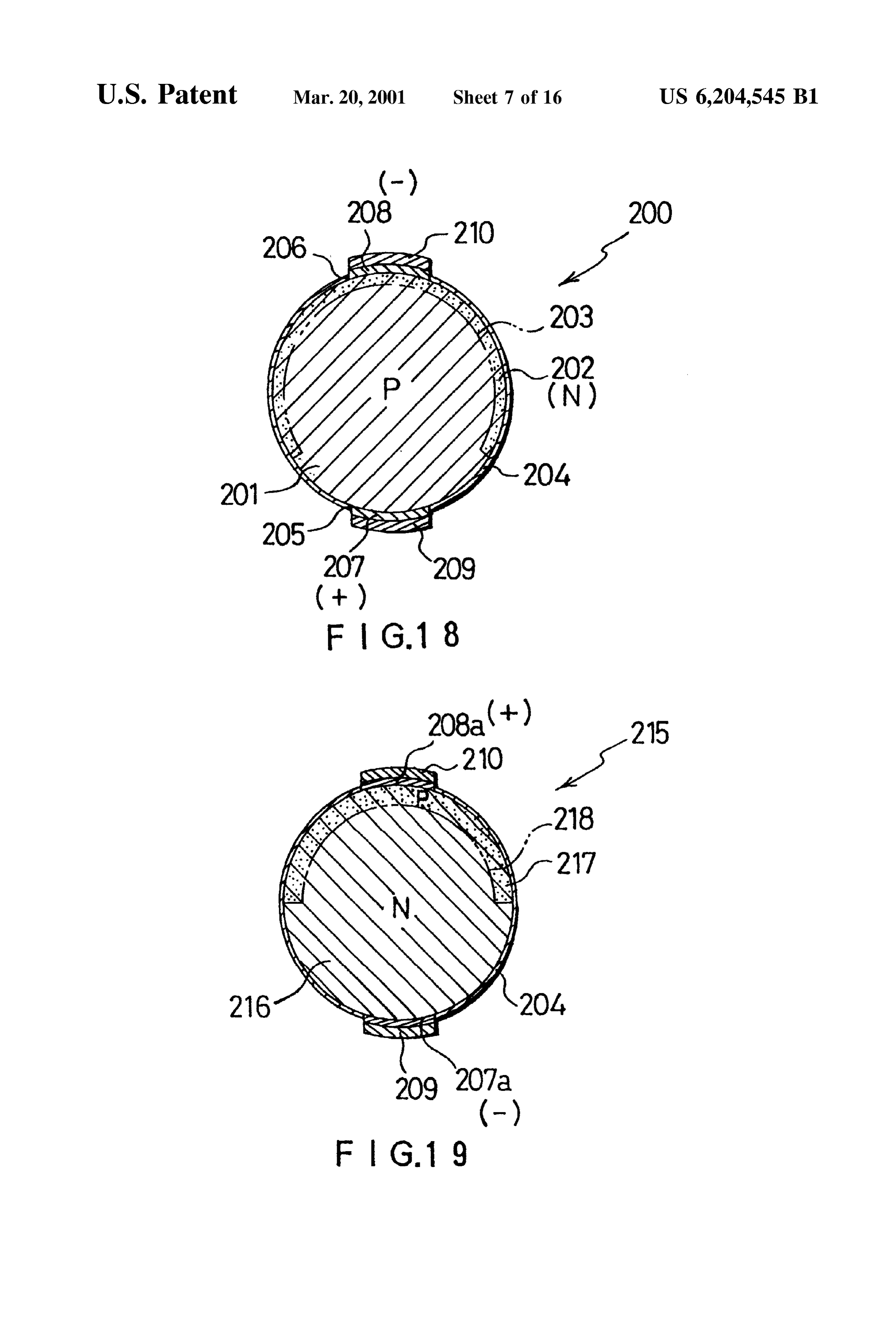
Semiconductor element number 1, there is formed a coating 50 FIGS. 18-28 are diagrams of Embodiment 2 of the which contains a phosphor which converts infrared light to present invention.
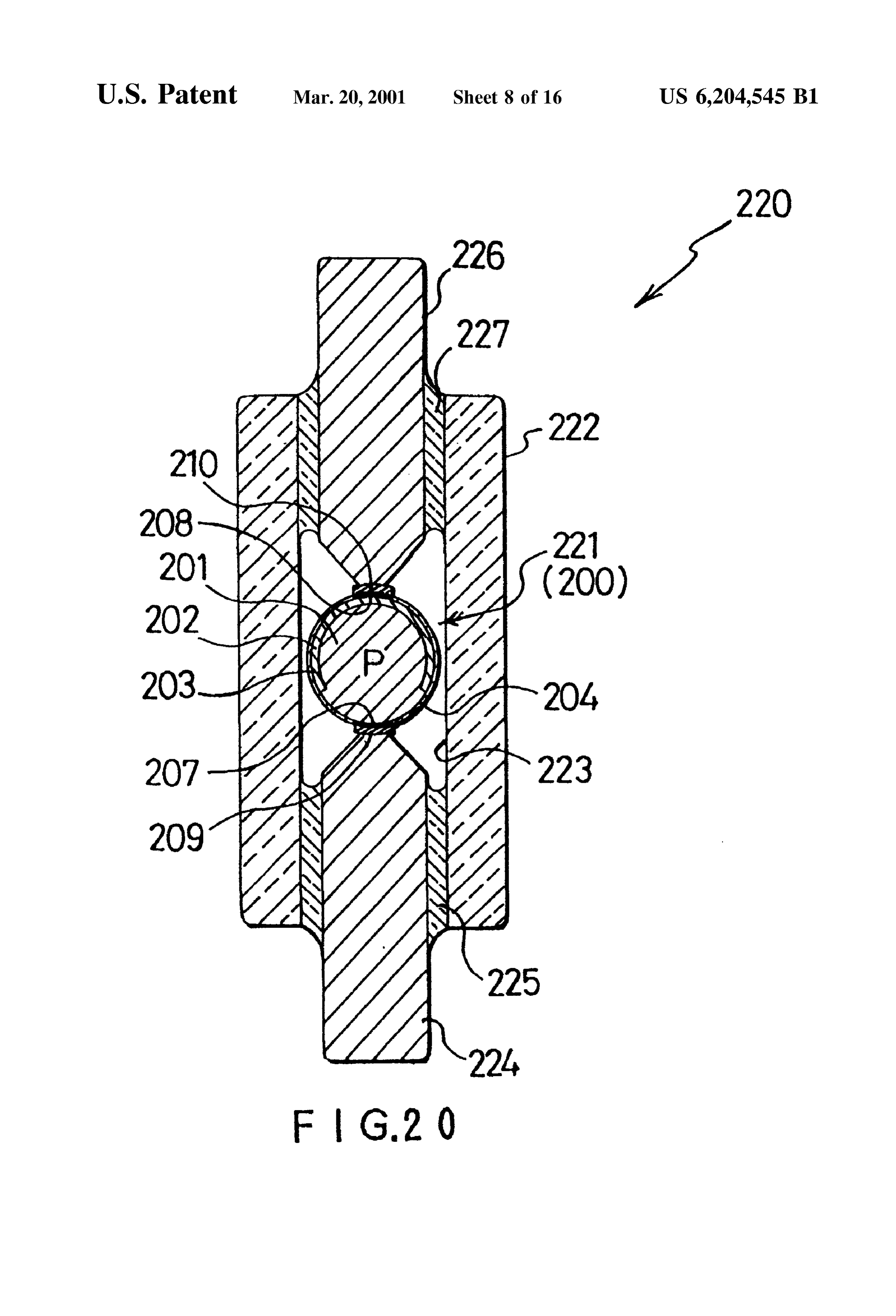
red light; on the Surface of the Spherical crystal of the FIG. 18 is a cross-sectional diagram of a Solar cell. Spherical Semiconductor element number 2, there is formed FIG. 19 is a cross-sectional diagram of a rectifier diode of a coating which contains a phosphor which converts infrared light to green light; on the Surface of the Spherical crystal of 55 a modification mode 1.
the Spherical Semiconductor element number 3, there is modification FIG. 20 is a cross-sectional diagram of a photodiode of a formed a coating which contains a phosphor which converts mode 2.
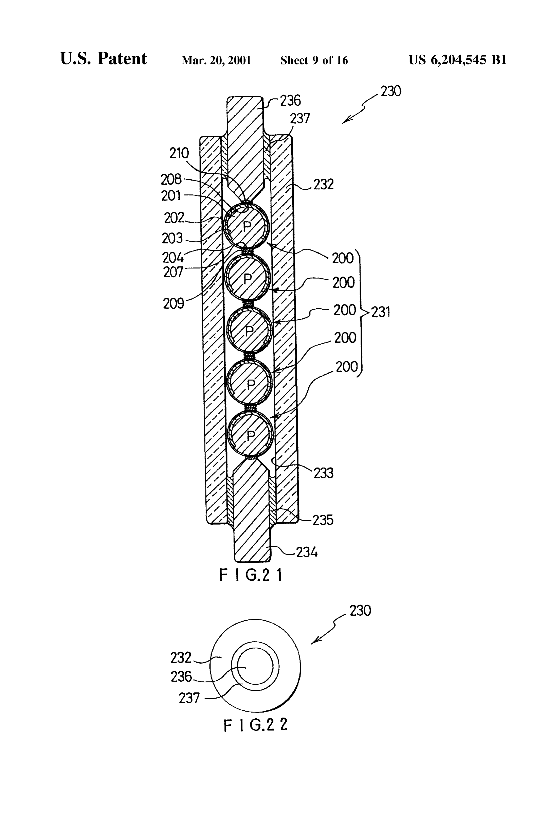
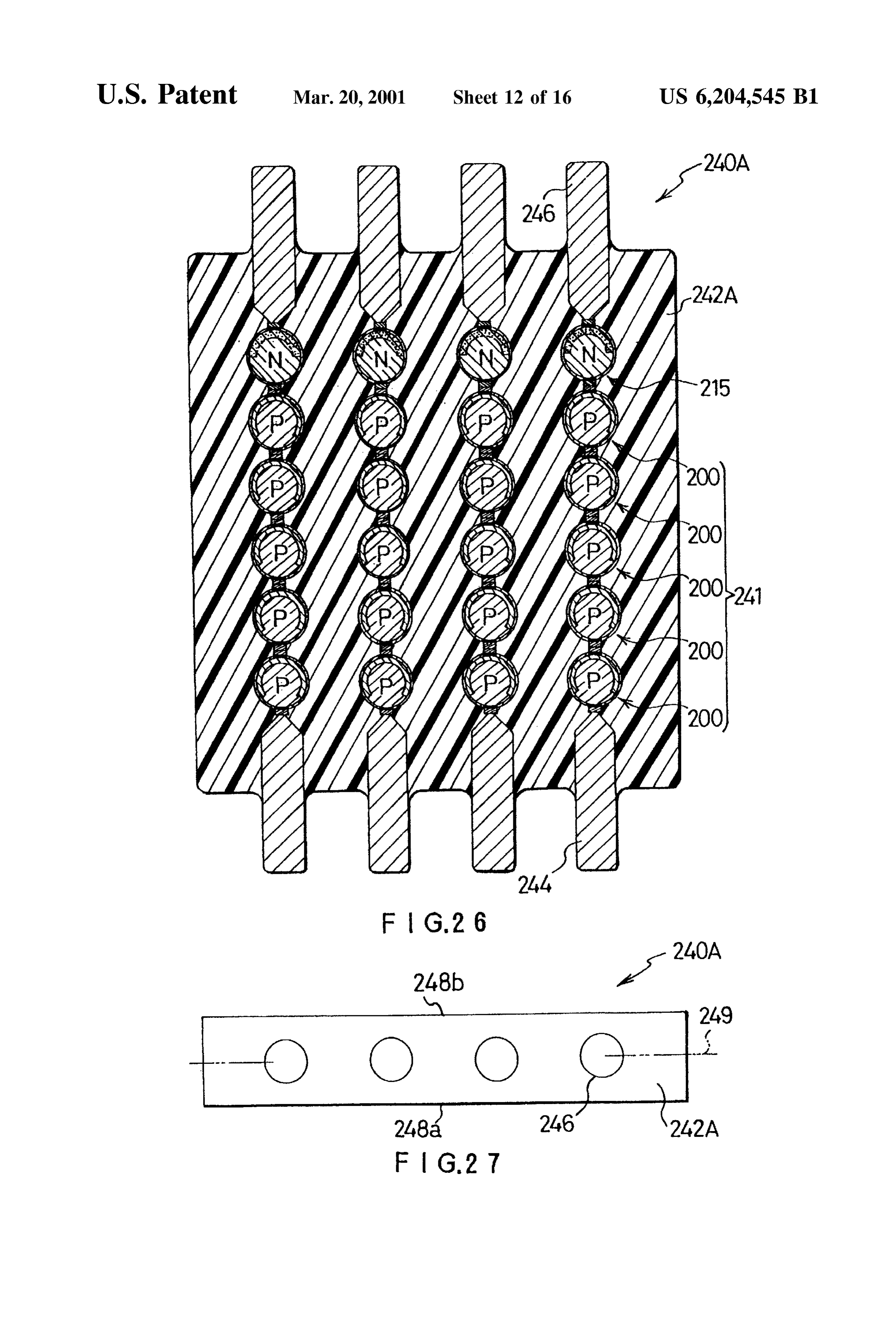
infrared light to blue light (claim 30 which is dependent FIG. 21 is a croSS-Sectional diagram of a Solar battery upon claim 29) In this manner, except for the coating which device of a modification mode 3. contains the phosphor, Spherical Semiconductor elements 60 FIG.22 is a plan view of the solar battery device of FIG. numbers 1-3 can be constructed with the same 21.
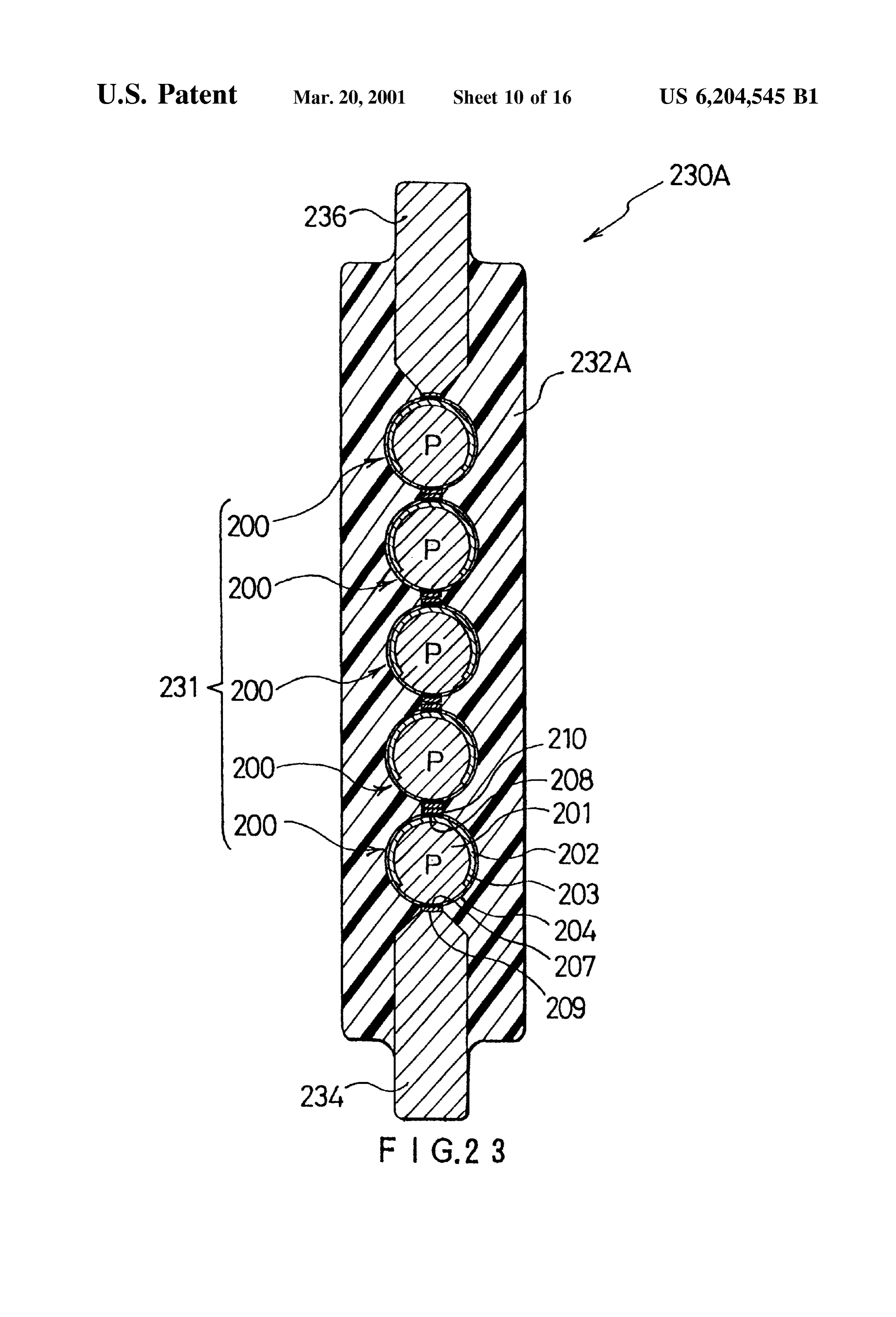
configuration, and they can be driven by the same driving FIG. 23 is a croSS-Sectional diagram of another Solar Voltage. battery device.
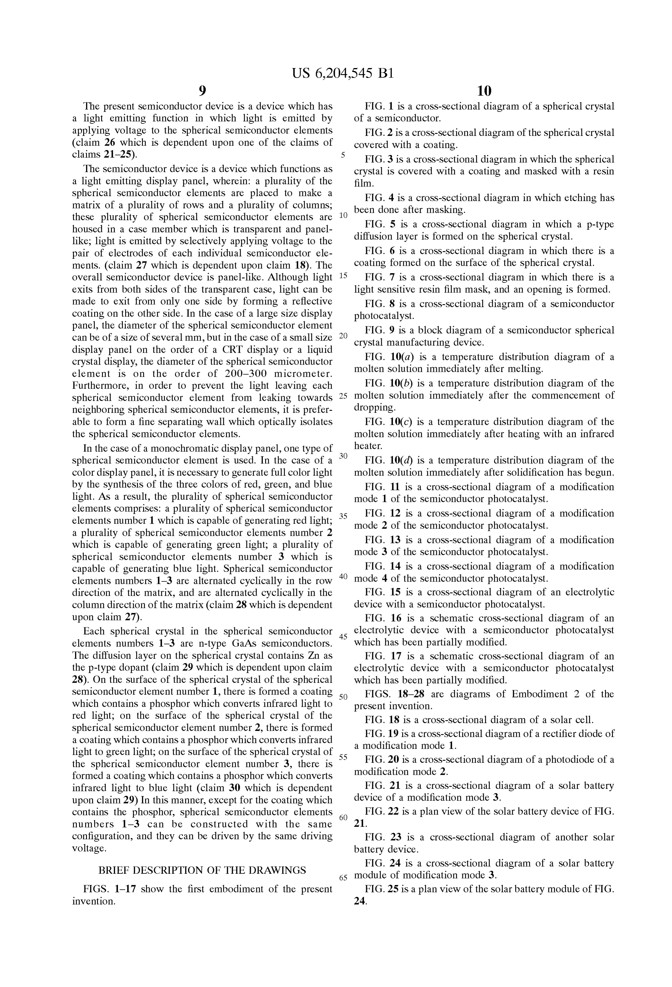
BRIEF DESCRIPTION OF THE DRAWINGS
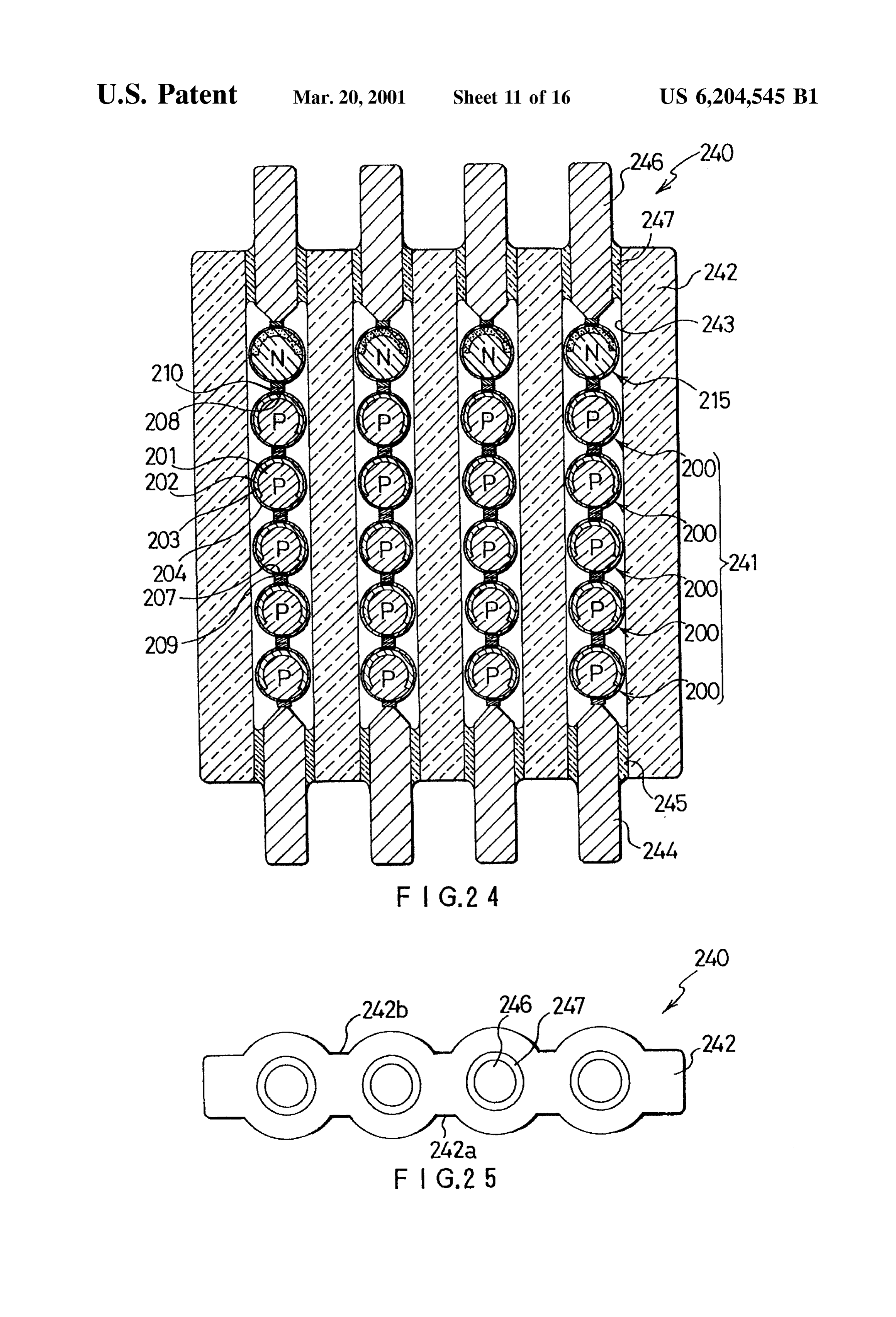
FIG. 24 is a croSS-Sectional diagram of a Solar battery 65 module of modification mode 3.
FIGS. 1-17 show the first embodiment of the present FIG.25 is a plan view of the solar battery module of FIG. invention. 24.
Page 23
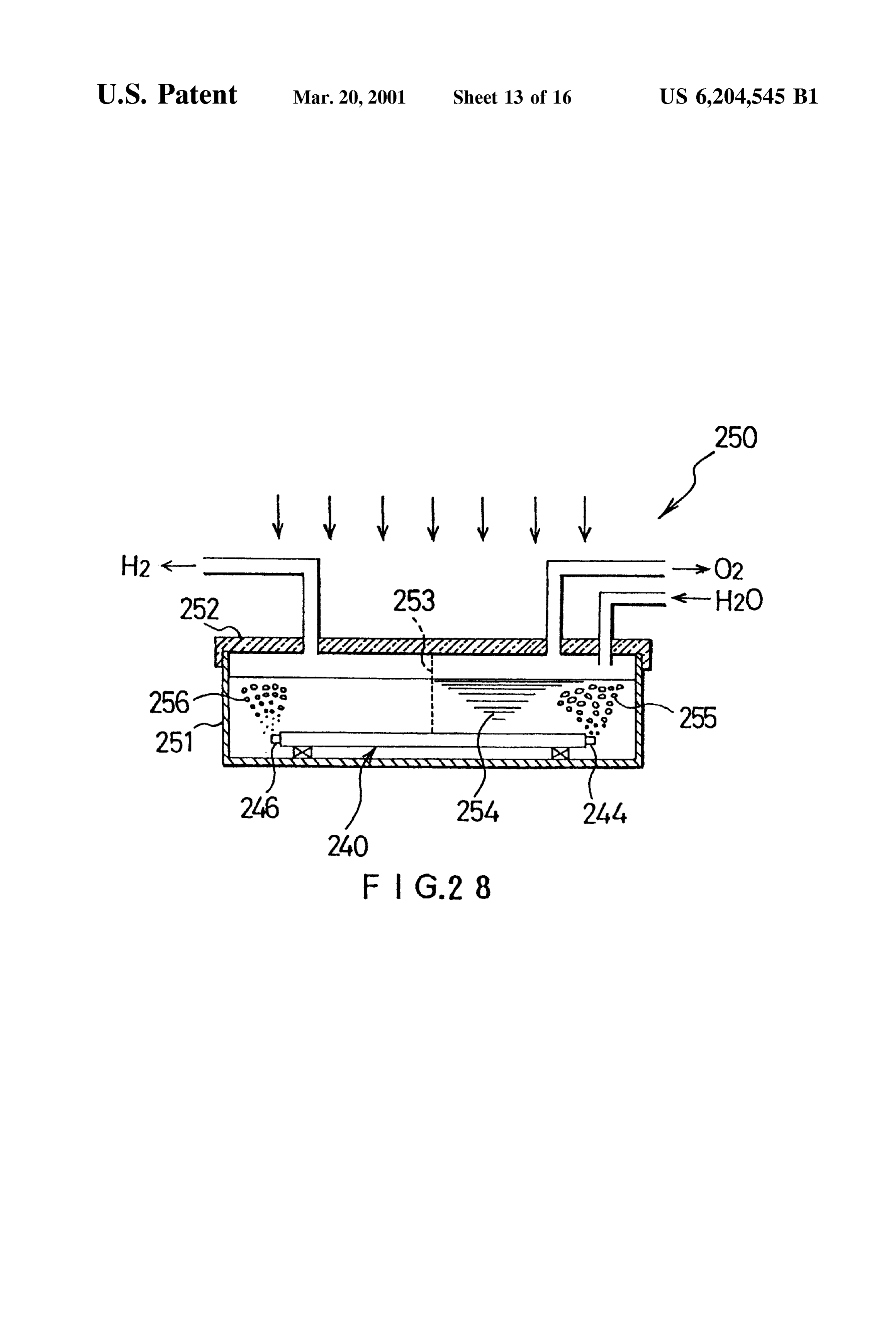
FIG. 26 is a cross-sectional diagram of another Solar the silicon semiconductor is solidified while it is free falling battery module. inside a drop tube. By doing this, Spherical crystal 2 with a FIG. 27 is a plan view of the Solar battery module in FIG. Smooth Surface can be produced. Furthermore, the crystal 26. Structure can be improved as needed by heating to a tem FIG. 28 is a cross-sectional diagram of the electrolytic perature of 600-900 degrees C. under an inert gas atmo device which uses a Solar battery module. sphere and annealing. Referring to FIGS. 9, 10, step 1 of the manufacturing method of Spherical crystal 2 will be
FIGS. 29–34 show Embodiment 3 of the present inven described later.
tion.
Next, referring to FIG. 2, in Step 2, Spherical crystal 2 is
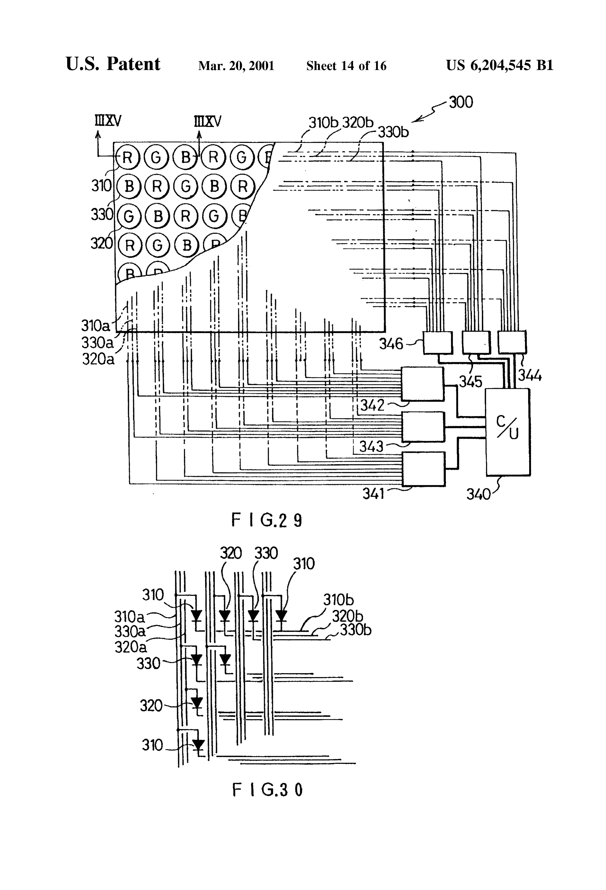
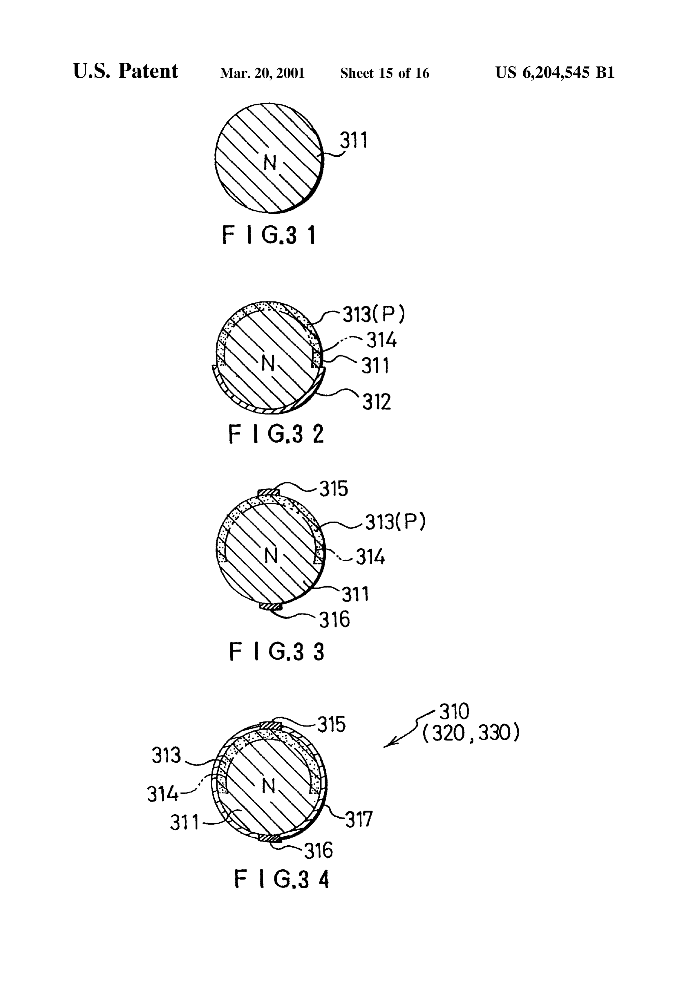
FIG. 29 is a block diagram of a display panel which heated to approximately 1150 degrees C. in an atmosphere incorporates light emitting diodes of 3 colors. which contains oxygen using a known method. A coating 3 FIG. 30 is a schematic drawing of an electrical circuit of of SiO2 (silicon oxide) of thickness 1 micrometer is formed a display panel. over the entire Surface of Spherical crystal 2. Next, referring FIG. 31 is a cross-sectional diagram of a spherical crystal to FIG. 3, in step 3, spherical crystal 2, on which there is of a Semiconductor. 15 formed coating 3, is placed on a Support plate 4 which is
FIG. 32 is a cross-sectional diagram of the Spherical made of glass, for example. A liquid-State resin film 5 which crystal which forms a pn junction with a p-type diffusion is an acid resistant Synthetic resin and has a thickness of layer. approximately the radius of Spherical crystal 2 is formed on FIG.33 is a cross-sectional diagram of a spherical crystal top of support plate 4. After covering the bottom half of which has electrodes. spherical crystal 2 with resin film 5, resin film 5 is made Solid.
FIG. 34 is a cross-sectional diagram of a light-emitting Next, in Step 4, using a diluted hydrofluoric acid Solution, diode.
portions of Spherical crystal 2 which are not covered by resin
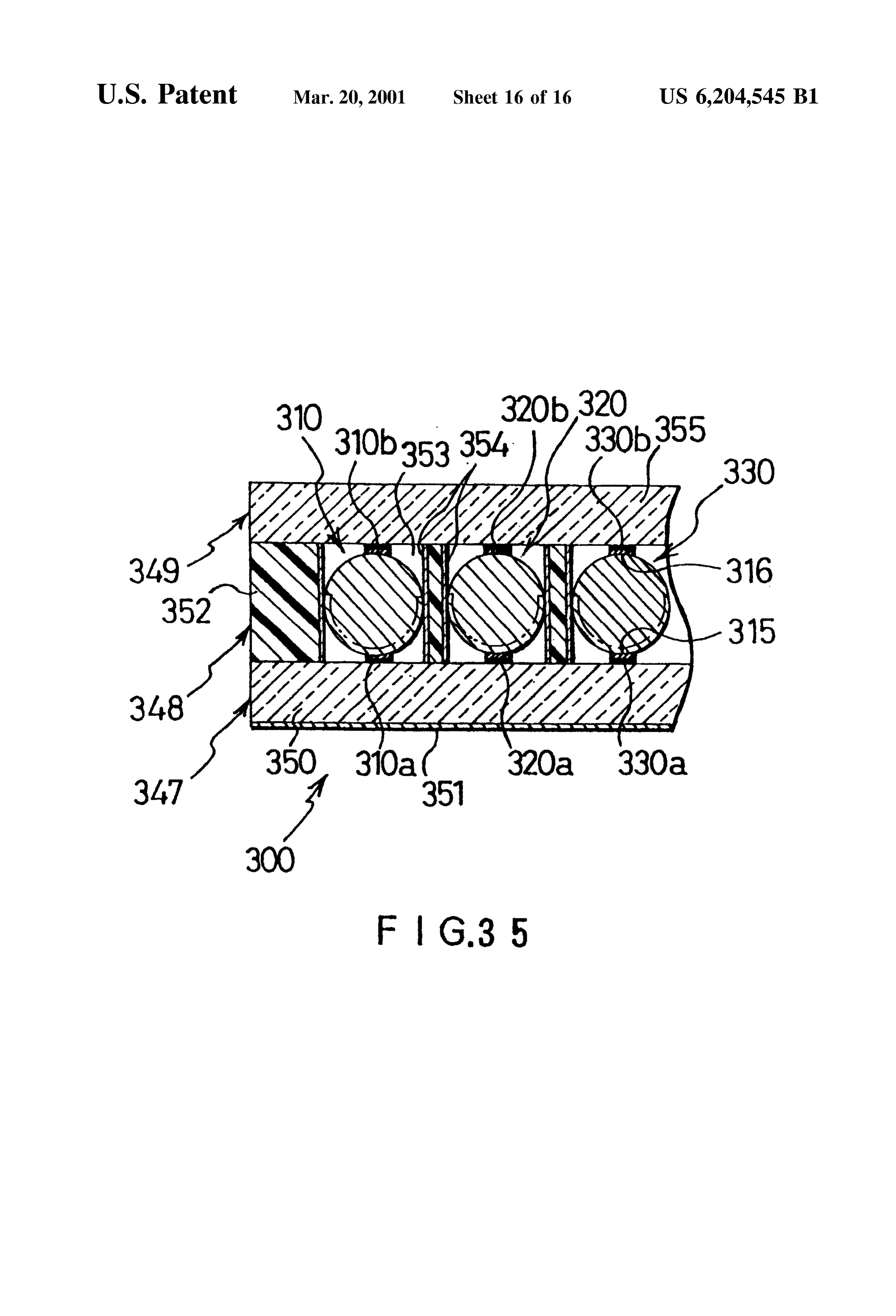
FIG. 35 is a cross-sectional drawing of FIG. 29 along the film 5 are etched. Coating 3 of SiO2 is dissolved and line IIIXV-IIIXV. 25 removed. Referring to FIG. 4, the result is shown. Next,
BEST MODE FOR CARRYING OUT THE referring to FIG. 5, in step 5, resin film 5 is dissolved using INVENTION a Solvent. Spherical crystal 2 is removed from Support plate 4. The surface of spherical crystal 2 is rinsed with an
Referring to the drawings, the best mode for carrying out appropriate cleaning Solution. Next, doping element for the the present invention will be described below. formation of a p type diffusion layer 6 is diffused by heating on the Surface of the upper half of spherical crystal 2 by a
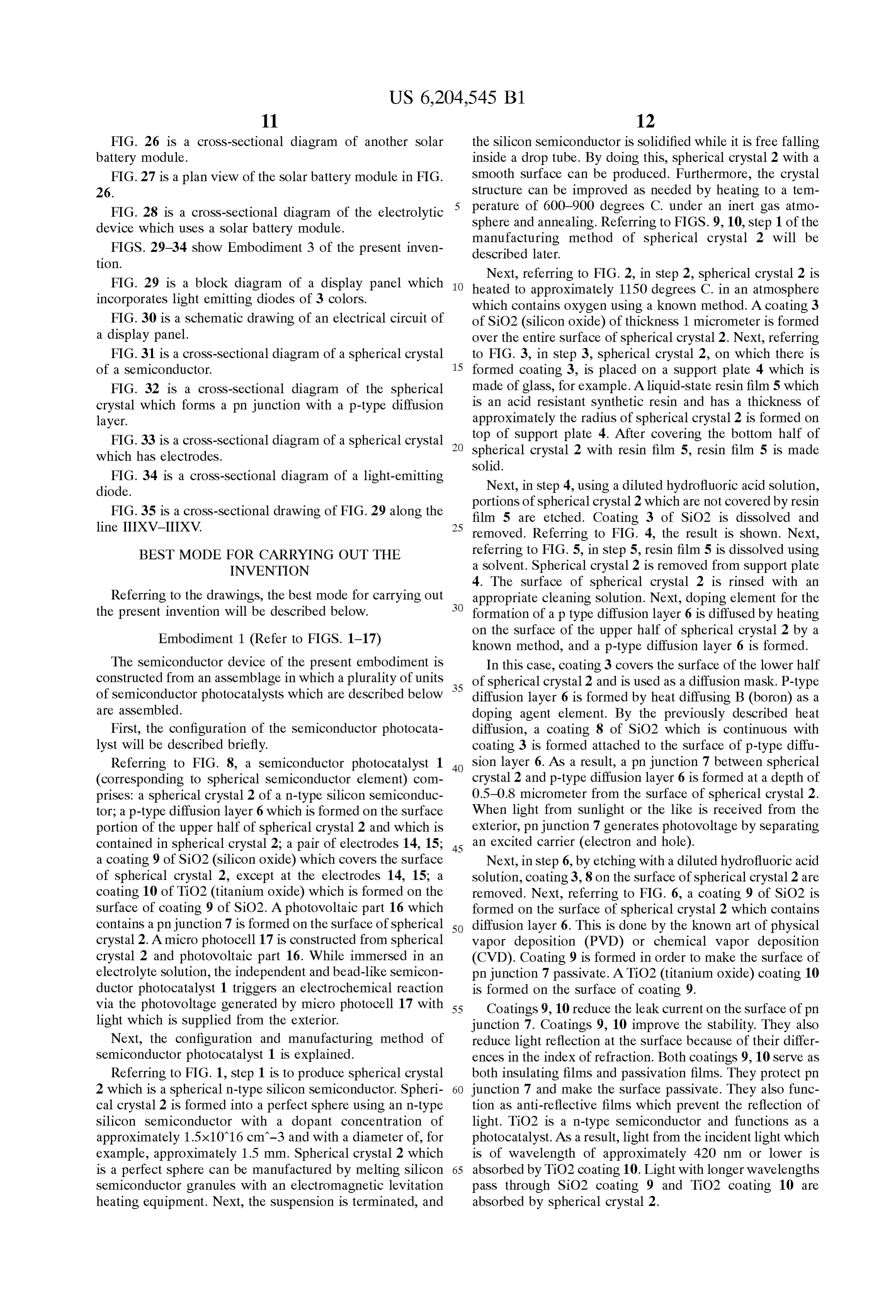
Embodiment 1 (Refer to FIGS. 1-17) known method, and a p-type diffusion layer 6 is formed. The semiconductor device of the present embodiment is In this case, coating 3 covers the Surface of the lower half constructed from an assemblage in which a plurality of units 35 of spherical crystal 2 and is used as a diffusion mask. P-type of Semiconductor photocatalysts which are described below diffusion layer 6 is formed by heat diffusing B (boron) as a are assembled. doping agent element. By the previously described heat First, the configuration of the Semiconductor photocata diffusion, a coating 8 of SiO2 which is continuous with lyst will be described briefly. coating 3 is formed attached to the Surface of p-type diffu Referring to FIG. 8, a semiconductor photocatalyst 1 40 Sion layer 6. AS a result, a pn junction 7 between Spherical (corresponding to spherical Semiconductor element) com crystal 2 and p-type diffusion layer 6 is formed at a depth of prises: a spherical crystal 2 of a n-type Silicon Semiconduc 0.5-0.8 micrometer from the surface of spherical crystal 2. tor; a p-type diffusion layer 6 which is formed on the Surface When light from Sunlight or the like is received from the portion of the upper half of Spherical crystal 2 and which is exterior, pnjunction 7 generates photovoltage by Separating contained in Spherical crystal 2, a pair of electrodes 14, 15; 45 an excited carrier (electron and hole). a coating 9 of SiO2 (silicon oxide) which covers the surface Next, in step 6, by etching with a diluted hydrofluoric acid of Spherical crystal 2, except at the electrodes 14, 15; a Solution, coating 3, 8 on the Surface of Spherical crystal 2 are coating 10 of TiO2 (titanium oxide) which is formed on the removed. Next, referring to FIG. 6, a coating 9 of SiO2 is surface of coating 9 of SiO2. A photovoltaic part 16 which formed on the Surface of Spherical crystal 2 which contains contains a pnjunction 7 is formed on the Surface of Spherical 50 diffusion layer 6. This is done by the known art of physical crystal 2. A micro photocell 17 is constructed from Spherical vapor deposition (PVD) or chemical vapor deposition crystal 2 and photovoltaic part 16. While immersed in an (CVD). Coating 9 is formed in order to make the surface of electrolyte Solution, the independent and bead-like Semicon pnjunction 7 passivate. A TiO2 (titanium oxide) coating 10 ductor photocatalyst 1 triggers an electrochemical reaction is formed on the surface of coating 9. via the photovoltage generated by micro photocell 17 with 55 Coatings 9, 10 reduce the leak current on the surface of pn light which is Supplied from the exterior. junction 7. Coatings 9, 10 improve the stability. They also Next, the configuration and manufacturing method of reduce light reflection at the surface because of their differ Semiconductor photocatalyst 1 is explained. ences in the index of refraction. Both coatings 9, 10 serve as Referring to FIG. 1, Step 1 is to produce Spherical crystal both insulating films and passivation films. They protect pn 2 which is a spherical n-type Silicon Semiconductor. Spheri 60 junction 7 and make the Surface passivate. They also func cal crystal 2 is formed into a perfect Sphere using an n-type tion as anti-reflective films which prevent the reflection of Silicon Semiconductor with a dopant concentration of light. TiO2 is a n-type Semiconductor and functions as a approximately 1.5x1016 cm-3 and with a diameter of, for photocatalyst. As a result, light from the incident light which example, approximately 1.5 mm. Spherical crystal 2 which is of wavelength of approximately 420 nm or lower is is a perfect Sphere can be manufactured by melting Silicon 65 absorbed by TiO2 coating 10. Light with longer wavelengths Semiconductor granules with an electromagnetic levitation pass through SiO2 coating 9 and TiO2 coating 10 are heating equipment. Next, the Suspension is terminated, and absorbed by spherical crystal 2.
Page 24
The thickness of both coatings 9, 10 are determined by mately 420 nm is absorbed by coating 10. By its photocata considering the following: their function as an passivation lytic action, a plurality of electrons and holes are generated. film for pn junction 7; the function of coating 10 as a The energy band gap curves at the Surface of TiO2 coating photocatalyst; the degree of transmittance with respect to the 10 where it is in contact with the phase boundary of the received spectrum; or the like. In the case of Silicon Semi electrolyte Solution or the like. A potential barrier Similar to conductor Spherical crystal 2, the thickness of SiO2 coating a Schottky barrier is created. As a result, the generated holes 9 is approximately 0.3-0.7 micrometer, and the thickness of move to positive electrode 14. At the interface, holes capture TiO2 coating 10 is approximately 0.3-1.0 micrometer. electrons and disappear after losing an amount of energy Next, referring to FIG. 7, in step 7, ohmic contacts which is close to the energy band obtained by the photo (electrodes 14, 15) are formed at the lower end of spherical excitation. This signifies the generation of oxidation action crystal 2 and at the top of p-type diffusion layer 6. These wherein electrons are captured at the Surface of TiO2 coating ohmic contacts are formed in a way that they are opposite 10. Simultaneously, at positive electrode 14, there is an each other, with the center of Spherical crystal 2 interposed oxidation action where electrons at the interface are captured between them. First, a pair of openings 11, 12 with diameters by the photovoltage provided by pn junction 7 of silicon. of approximately 0.5 mm are formed on the transparent two 15 TiO2 coating 10 is electrically in contact with positive layers of coatings 9, 10. This is accomplished by known electrode 14. As a result, compared with TiO2 alone, the methods of photolithography or plasma etching or the like. photovoltage provided by pnjunction 7 is applied as a bias. In this case, the pair of openings 11, 12 are formed while The oxidation potential is heightened, and the capturing of masking with a corrosion-resistant photoresist 13. higher energy electrons becomes possible. Negative elec Next, in step 8, from the pair of openings 11, 12 in FIG. trode 15 exhibits its reducing action, where electrons are 7, Ti (titanium) is vapor deposited onto spherical crystal 2 given up to the exterior at the phase boundary of the using known vapor deposition methods. Next, Ni (nickel) is electrolyte Solution or the like. In this manner, Semiconduc tor photocatalyst 1 exhibits its capacity as a photocatalyst
Vapor deposited. A pair of ohmic contacts of thickneSS which automatically triggers an electrochemical reaction 0.1-1.0 micrometers are formed. Afterwards, they are sin 25 with only the input of light.
tered at 200-300 degrees C. in a vacuum. Corrosion resistant, photoresist 13 is ashed and removed. In this Semiconductor photocatalyst 1 which is described above manner, a positive electrode 14 is formed at the top of p-type has the following effects.
diffusion layer 6 of spherical crystal 2, and a negative (a) a micro photocell 17 is constructed by forming on electrode 15 is formed at the bottom of spherical crystal 2. Spherical crystal 2, a photovoltaic part 16 which works Electrodes 14, 15 become the entrance and exit for the together with Spherical crystal 2 to generate photovoltage. inflow and outflow of current with respect to the outside There is formed TiO2 coating 10 which has a photocatalytic circuit. Independent and bead-like Semiconductor catalyst 1 function and which is electrically connected to positive as shown in FIG. 8 is obtained in this manner. An example electrode 14. As a result, the activation voltage is lowered at of the manufacture of a single Semiconductor photocatalyst 35 electrodes 14, 15. A semiconductor photocatalyst with high was described above, but in practice, Several Semiconductor energy conversion efficiency is obtained. photocatalysts are manufactured at once. (b) By appropriately combining the energy band gap of pn AS described later, an assemblage of Several Semiconduc junction 7 of Silicon Semiconductor Spherical crystal 2 and tor catalysts 1 are immersed in a pre-Selected electrolyte the energy band gap of the metal oxide Semiconductor which Solution, and it can be used to trigger electrochemical 40 has photocatalytic function, Such as TiO2, or the like, the reactions by Shining light from outside. Materials which potential difference between the electrodes can be made to have a catalytic function are the preferred material for be a suitable potential difference for the electrochemical electrodes 14, 15. The selection of material depends on what reaction. The Selectivity for the necessary reaction products is to be generated with the dissociation reaction. Reaction can be increased.
activity and reaction Selectivity are used as a basis for 45 (c) The Surface of spherical crystal 2 is electrochemically Selection. For example, in the electrolysis of water, Ru, Ir, as protected with a thin oxide film Such as TiO2 which is well as the previously described Ni, or their oxides are photochemically Stable and which has a large energy band preferred for the hydrogen generating reducing electrode. gap. The thin oxide film also exhibits functions as a photo When CO2 gas is photoreduced by water, Pd, Rh or the like catalyst and as an anti-reflective film. As a result, manufac is the preferred material for the CH4-gas producing reducing 50 turing costs are lowered. A Semiconductor photocatalyst 1 electrode. which has a high energy conversion efficiency and high Next, the operation of Semiconductor photocatalyst 1 is reliability can be realized.
explained. (d) Semiconductor photocatalyst 1 is formed as a com AS an example, the following situation will be described: paratively Small sphere. A sphere has excellent mechanical Semiconductor catalyst 1 is immersed in an electrolyte 55 Strength and is difficult to destroy. Because it can freely Solution; light is Shined from the outside; and there is move in a liquid, they can be dispersed in necessary places. electrolysis of the electrolyte solution. When a light such as Furthermore, positive electrode 14 and negative electrode 15 Sunlight which has a wide spectrum distribution is Shined on are opposite each other with the center of Spherical crystal Semiconductor catalyst 1, a photovoltage, in which positive 2 interposed between them. As a result, while light is being electrode 14 becomes positive and negative electrode 15 60 Shined, it is possible to electrically connect a plurality of becomes negative, is generated. This happens as a result of Semiconductor photocatalysts 1 in a Series by applying an light which has been transmitted through coatings 9, 10 and electric field from the outside.
which is absorbed pn junction 7 and its rear region. (e) Because Semiconductor photocatalyst 1 receives light The maximum open circuit Voltage which is generated from the Sphere Surface, the influence of the angle of between electrodes 14, 15 is 0.6V. When there is incident 65 incidence of the light is Small. There is a high Sensitivity to light on the Surface of TiO2 coating 10 which is a n-type light with a wide incidence directions Such as Scattering Semiconductor, light with a wavelength below approxi light.
Page 25
(f) In step 1 of the manufacturing of spherical crystal 2, line of force acting on the induced current are balanced it is molten in a levitated State. The Surface tension of the between the upward force and downward force. Solid mate melt is used to create the Sphere and to have it Solidify. AS rial 2a is maintained in a levitated State. Solid material 2a is a result, there is no mechanical StreSS and lattice defects heated by the heat generating action of the induced current. remaining in Spherical crystal 2. There are no problems of When solid material 2a becomes molten liquid material 2b, impurity contamination which get mixed in from the con the high frequency current is shut down. Molten liquid tainer which Stores the molten liquid, and a high quality material 2b begins a free-fall. With this free-fall, molten substance is obtained. When a sphere crystal is made by liquid material 2b becomes Spherical by the action of Surface letting the molten solution solidify while it free falls inside tension under a very small gravitational force of 10^-5. a drop tube, the quality is particularly good, with a good
The purpose of infrared heater 113 is for heating only the
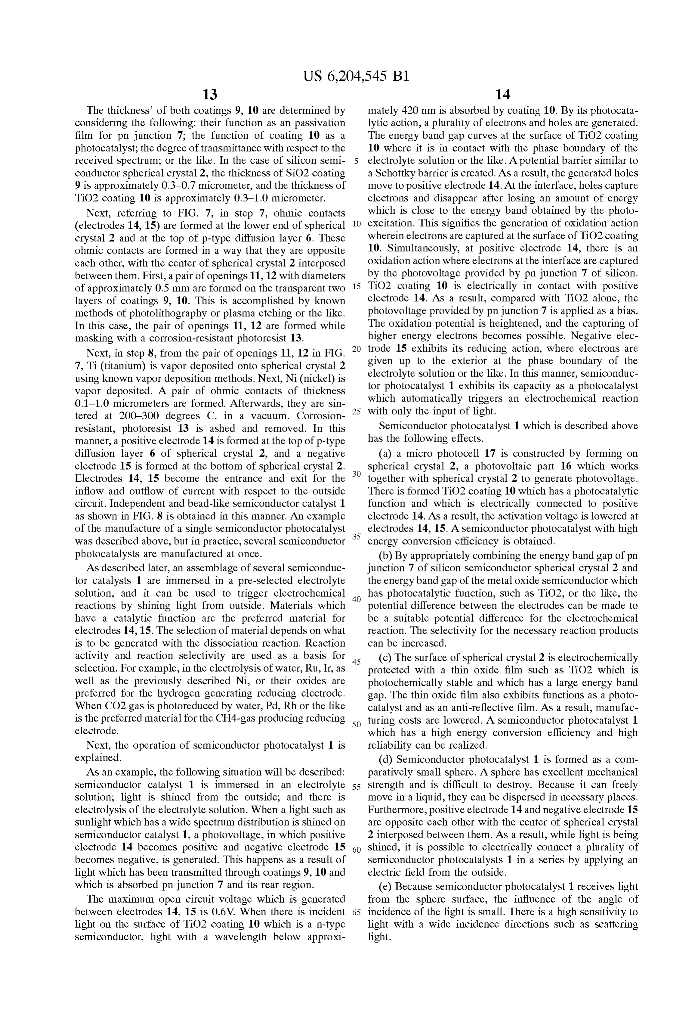
Sphericity, uniform distribution of the constitution, and few Surface crystal defects. of molten liquid material 2b by a Small amount. Next, the Spherical crystal manufacturing device which Infrared heater 113 is placed as a ring around the outside of creates Silicon Semiconductor Spherical crystal 2 of Step 1 is drop tube 110. Infrared heater 113 is placed at a certain described. The method of manufacturing Spherical Semicon 15 distance equipment away from electromagnetic levitation heating 112. Infrared heater 113 comprises a cylindrical ductor crystals is also described. heater body which is made of an infrared radiation ceramics. Referring to FIG. 9, a spherical crystal manufacturing By controlling the current which is Supplied to this heater device 101 comprises: a vertical drop tube 110 which has a body, the heating function can be controlled precisely. diameter of 5-10 cm and a height of approximately 14m; an Because molten liquid material 2b rotates while free falling, electromagnetic levitation heating equipment 112 which is only the Surface of molten liquid material 2b is heated placed on the outside of the upper part of drop tube 110; an evenly by infrared heater 113.
infrared heater 113 which is an after heater; a material
Supply device 111 which Supplies Solid material 2a one at a turing Next, the operations will be described where manufac time; a silicon oil chamber 115 which is housed in a housing n-type device
Silicon 101 is used to make Spherical crystal 2 from
Solid material 2a. In the first preparation Stage, area 114 which is continuous with the lower end of drop tube 25 electromagnetic valves 123, 136, 137, 138 are opened. 110; a vacuum pump 116 which suctions air from inside drop Vacuum pump 116 is operated, and Specified vacuum con tube 110, a gas Supply device 117; a pipe System and valves, high speed cameras 118a–118c, a control unit 120 which ditions are created inside drop tube 110. A single solid controls these apparatus. Furthermore, floors 1-5 of the material 2a is Stored in receiving apparatuS 126. There is a pre-determined current flowing through infrared heater 113.
factory are depicted as floors 103a–103e.
Material Supply device 111 comprises: a Supplier 121; a Next,ing current is run through electromagnetic levitation heat equipment 112. Electromagnetic Shutter 130 is opened, parts feeder 122 which Stores Several granular Solid material and Solid material 2a and which supplies them one at a time. Parts feeder 122 Solid material 2a is2a heated free-falls. While in a levitated State, by electromagnetic levitation has a function of pre-heating Solid material 2a and a function heating equipment 112 for a specified Short amount of time. for evacuation of atmosphere. A case 123 of a Supplier 121 35 Solid material 2a becomes molten liquid material 2b. Refer is connected to vacuum pump 116 by a Suction pipe 125 which has an electromagnetic Switch valve 124. A receiving ring to FIG. 10(a), the temperature distribution of molten apparatus 126 is connected to parts feeder 122 by a pathway liquid roughly material 2b at this time is Such that the temperature is the same in both the interior and on the Surface of 128 which has an electromagnetic shutter 127. There is an molten liquid material 2b.
electromagnetic shutter 130 at an exit pathway 129 of 40 receiving apparatus 126. Vacuum from inside case 123 is Next, the current to electromagnetic levitation heating introduced via a plurality of Small holes to receiving appa equipment 112 is shut off. Molten liquid material 2b begins ratus 126. During the operation of manufacturing device a free fall in the vacuum of drop tube 110. Because liquid 101, electromagnetic valve 124 is opened, and there is a molten material 2b is under microgravity conditions, after Vacuum inside Supplier 121. When Supplying Solid material 45 the commencement of the free-fall, molten liquid material 2a from parts feeder 122, electromagnetic shutter 130 is 2b becomes Spherical by the action of Surface tension. closed. Electromagnetic Shutter 127 is opened, and after Molten liquid material 2b initially falls with a low speed. In Solid material 2a is Supplied to the inside of receiving the short time it takes to fall to the level of the upper end of apparatus 126, electromagnetic Shutter 127 is closed. There heatinfrared heater 113, there is radiative cooling, and there is are electromagnetic valves 136-138 on Suction pipes 50 release. Because there is heat release from the Surface 133-135 which are connected to vacuum pump 116. In order of molten liquid material 2b, the Surface of molten liquid to allow inert gases or oxidizing gases to flow inside drop material 2b is cooler than the interior (refer to temperature tube 110 as needed, there are a gas Supply device 117, a gas distribution in FIG. 10(b)).
supply pipe 139, branching pipes 139a, 139b, a gas dis Next, during the free fall of the molten liquid material 2b charge pipe 141, and electromagnetic valves 140, 142. 55 through the interior of infrared heater 113, only the surface However, if a vacuum is to be maintained inside drop tube is heated. Referring to FIG. 10(c), the surface of liquid 110, gas Supply device 117 is stopped, and electromagnetic molten material 2b is warmer than the interior. Next, while valves 140, 142 are closed. it is free falling towards the bottom of infrared heater 113, Electromagnetic levitation heating equipment 112 is con molten liquid material 2b releases heat through radiative Structed from an upper coil, a lower coil, and a high 60 cooling. By the action of Surface tension, molten liquid frequency current generating device 119, and the like. An material 2b Solidifies to a truly Spherical crystal 2. upward force of magnetic line is generated by the upper coil. After passing through infrared heater 113, radiative cool A downward magnetic line of force is generated by the lower ing progresses. Referring to FIG. 10(d), the temperature coil. An induced current is generated in Solid material 2a by distribution of molten liquid material 2b when the tempera the magnetic lines of force which change at a high fre 65 ture has dropped to near the Solidifying point T0 is indicated quency. When Solid material 2a is at a central position by the solid line or the dotted line. Because solidification between the upper and lower coils, the force of the magnetic begins with these conditions, Solidification begins from the
Page 26
interior and from the Surface of molten liquid material 2b. AS Furthermore, the electric potential between the oxidation a result, even if there is volume expansion during and reducing electrodes can be made large.
Solidification, there are no projections formed on the Surface Modification mode 2 . . . (refer to FIG. 12) of spherical crystal 2. The inner mechanical StreSS of Spheri Next, Semiconductor photocatalyst 1B which is a partial cal crystal 2 also becomes very Small. Afterwards, Spherical modification of semiconductor photocatalyst 1 will be crystal 2, which has finished Solidification at around the described. However, the description of elements which have middle level of drop tube 110, drops into silicon oil inside the same numerals as those which have been described silicon oil chamber 115. They are stored there and are cooled previously are abbreviated. Referring to FIG. 12, a SiO2 completely. Even though the interior distortions is reduced coating 9A (thickness 0.3-0.7 micrometer) covers the Sur in Spherical crystal 2 described above, if the Overall spheri face of the lower half of spherical crystal, except at the cal crystal 2 does not become a monocrystal, afterwards, surface of negative electrode 15. An Si3N4 coating 20A Spherical crystal 2 can be made into a monocrystal through (thickness approximately 0.3-1.0 micrometer) covers the anneal processing. surface of coating 9A. These coatings 9A and 20A are Spherical crystal 2 which is truly spherical and which is formed by PVD or CVD method. A TiO2 electrode coating without any projections can be manufactured in the above 15 22 (thickness approximately 0.3-0.7 micrometer) covers a manner. Even if there are projections which have formed, large portion of the surface of p-type diffusion layer 6. TiO2 they are extremely Small projections which can be elimi electrode coating 22 is formed So that it does not contact pn nated during the annealing process. Furthermore, because junction 7. A hetero-unction 23 is formed between p-type the surface of molten liquid material 2b does not solidify diffusion layer 6 and coating 22. The energy band gap of before the inside does, any bubbles on the surface of solid hetero-junction 23 is different from p-type diffusion layer 6. material 2a does not mix in Spherical crystal 2. Because When manufacturing Semiconductor photocatalyst 1B, molten liquid material 2b Solidifies to Spherical crystal 2 coatings 9A, 20A are formed over the entire surface of under microgravity conditions, a spherical crystal 2 with an Spherical crystal 2 including p-type diffusion layer 6. uniform constitutional distribution with no influence from Afterwards, the areas which correspond to electrode coating heat convection, buoyancy, Sedimentation is achieved. 25 22 are removed by etching, and electrode coating 22 is Modification mode 1 ... (refer to FIG. 11) formed. An opening can be formed in coatingS 9A, 20A in Next, Semiconductor photocatalyst 1A which is a partial order to form negative electrode 15. The manufacturing modification of semiconductor photocatalyst 1 will be method is not limited to this, but Semiconductor photocata described. However, the description of elements which have lyst 1B can be manufactured by various known techniques. the same numerals as those which have been described When light such as Sunlight or the like is shined on previously are abbreviated. Referring to FIG. 11, in this Semiconductor photocatalyst 1B, holes accumulate at the Semiconductor photocatalyst 1A, instead of TiO2 coating Surface of electrode coating 22. It functions as an oxidizing 10, there is a Si3N4 (silicon nitride) coating 20 (thickness electrode which takes electrons at the phase boundary. The approximately 0.3-0.7 micrometer) which is formed by photovoltage of micro photocell 17 increases the Surface PVD or CVD method. Furthermore, a TiO2 electrode coat 35 electric potential of electrode coating 22. It functions in the ing 21 (thickness approximately 1.0 micrometer) is formed Same manner as Semiconductor photocatalyst 1A of modi by PVD or CVD method. Electrode coating 21 covers a large fication mode 1. Because there is no metallic positive proportion of the Surface of the upper half of Spherical electrode which can obstruct incident light, the entire Surface crystal 2, including the Surface of positive electrode 14. of electrode coating 22 functions as an efficient photocata Because positive electrode 14 is masked by TiO2 electrode 40 lyst. Because the barrier height of hetero-junction 23 is coating 21, a direct eXchange of electrons with the outer reduced by light generated carriers, the photochemical con interface is not possible. Instead, electrode coating 21 func version efficiency is heightened. tions as a positive electrode which has an oxidative action. Modification made 3. ... (refer to FIG. 13) AS described previously, because the energy band is bent Next, Semiconductor photocatalyst 1C which is a partial at the surface of TiO2 electrode coating 21, a plurality of 45 modification of semiconductor photocatalyst 1 will be electron and hole pairs are generated when light is received. described. However, the description of elements which have Holes accumulate at the phase boundary. This becomes a the same numerals as those which have been described positive electric potential compared with negative electrode previously are abbreviated. Referring to FIG. 13, spherical 15, and it acts in a way to run current to the outside. When crystal 2A is a Spherical crystal of an n-type Silicon Semi this current flows, an oxidation reaction is generated at the 50 conductor without the p-type diffusion layer 6. On the Surface of electrode coating 21 which has a photocatalytic Surface of spherical crystal 2A, a SiO2 coating 24 (thickness function. A reduction action is generated at negative elec 1.5-3.0 nm) covers the entire Surface, except at negative trode 15. When semiconductor photocatalyst 1A receives electrode 15. A metal coating 25 (thickness approximately Sunlight, TiO2 electrode coating 21 absorbS light at wave 10-15 nm) covers the surface of coating 24 at the top half lengths shorter than approximately 410 nm. Light with 55 of Spherical crystal 2A. Metal coating 25 is, for example, a longer wavelengths are absorbed by micro photocell 17. Ti or Nicoating. With this MIS configuration there is a The photovoltage generated at pnjunction 7 is a bias with bending of the energy band Similar to a pn junction at the respect to electrode coating 21 and heightens the Surface interface of spherical crystal 2A and SiO2 coating 24 electric potential of electrode coating 21. As a result, the underneath metal coating 25. There is formed a photovoltaic oxidation Voltage at electrode coating 21 is heightened, and 60 part 16C which contains an energy band bending layer 6C the electrical energy which is available for electrochemical near the surface, and there is formed a microphotocell 17C. reactions is heightened. TiO2 has a larger energy band gap Modification mode 4. ... (refer to FIG. 14) than the Silicon Semiconductor of Spherical crystal 2, and it Next, Semiconductor photocatalyst 1D which is a partial also absorbs short wavelength light to photo-excite electrons modification of semiconductor photocatalyst 1 will be and holes. Because electrode coating 21 is formed from 65 described. However, the description of elements which have TiO2, light Such as Sunlight, which has a wide spectral the same numerals as those which have been described distribution, can be efficiently converted to chemical energy. previously are abbreviated. Referring to FIG. 14, spherical
Page 27
crystal 2A is a Spherical crystal of an n-type Silicon Semi electrolyte Solution chamber 32 and which applies a com conductor without the p-type diffusion layer 6. On the upper mon electric field to the plurality of Semiconductor photo half of spherical crystal 2A, a metal coating 27 (thickness catalysts, a power Supply device 36 which applies a speci approximately 10-15 nm) is formed. Metal coating 27 is, for fied serial voltage between positive electrode 34 and example, a Ti or Nicoating. An SiO2 insulating coating 9D negative electrode 35; a glass cover 33 for collecting gas (protective film) (thickness approximately 0.3-0.7 which is generated; a pipe 37 which replenishes electrolyte micrometer) covers the surface of the lower half of spherical Solution 31; a gas exit pipe 38 through which generated gas crystal 2A, except at electrode 15. With this Schottky barrier is removed.
construction, there is a bending of the energy band Similar to When conducting electrolysis using electrolysis device at a pn junction at the interface of Spherical crystal 2A and 30, an aqueous Solution of methanol, for example, of a metal coating 27. There is formed a photovoltaic part 16D specified concentration fills electrolyte solution chamber 31 which contains an energy band bending layer 6D near the to a specified depth. Sunlight 41 is shined from above, and surface, and there is formed a microphotocell 17D. photovoltage is generated in a plurality of Semiconductor The Semiconductor photocatalyst of the present invention photocatalysts 1. A Serial Voltage is applied from positive is not limited to what has been described above. The 15 electrode 34 to negative electrode 35 via electrolyte solution following changes can be added. 31.
(1) TiO2 coating 10 and electrode coatings 21, 22 which Almost all of the Semiconductor photocatalysts is given a are used as photocatalysts and which have a large energy direction by the electric force as a result of the bipolar band gap are not absolutely necessary. TiO2 coating 10 can phenomenon. Negative electrode 15 of each of the semi be omitted. For the objectives of passivation and anti conductor photocatalysts 1 faces towards positive electrode reflection, an Si3N4 coating can be formed on the surface of 34, and positive electrode 14 face toward negative electrode SiO2 coating 9 so that the entire microphotocell 17 is 35. 2-4 of the semiconductor photocatalysts become elec protected. In this case, the oxidation-reduction Voltage is trically connected in Series. Even if the application of Serial limited by the open circuit Voltage of pnjunction 7 generated Voltage is terminated afterwards, the Serial connection con between positive electrode 14 and negative electrode 15. But 25 tinues. Under these conditions, electrolysis device 30 is the catalytic action of electrodes 14, 15 still remain. operated. Electrolysis of electrolyte Solution 31 occurs. (2) Spherical crystal 2 can be constructed of p-type Silicon Electrolyte solution 31 (methanol solution) is oxidized at Semiconductor. Instead of a p-type diffusion layer 6, an positive electrode 14 and at the surface of TiO2 coating 10 n-type diffusion layer can be formed. Furthermore, the which is in contact with positive electrode 14. The solution n-type or ptype Semiconductor which is to be used for is reduced at the Surface of negative electrode 15. As a result, Spherical crystal 2, 2A is not limited to Si Semiconductor, but CO2 gas 40 is generated at positive electrode 14 and at the semiconductors of SiGe, SiC, or the like, Group III-V surface of coating 10. H2 gas 39 is generated at the surface compound Semiconductors of GaAS or InP or the like, of negative electrode 15.
chalcopyrite SemiconductorS Such as CuInSe2 or the like can The mixture gas of generated CO2 gas 40 and H2 gas 39 also be used. Pnjunction 7 can be a hetero-junction. Refer 35 is guided by cover 33 and is sent to a gas tank (not shown) ring to FIG. 13, this MIS configuration is only one example, from gas exit pipe 38. The mixture gas is separated by a gas and various MIS configurations can be used. Referring to Separating device which is connected to the gas tank. In FIG. 14, this Schottky barrier configurations is only one electrolysis device 30, the individual semiconductor photo example, and various Schottky barrier configurations can be catalysts 1 are not anchored to electrolyte Solution chamber used. 40 32. When light Stops Shining, they can be moved indepen (3) Materials which can be used as an anti-reflective film dently. They can be dispersed in places where they are and which have passivating function, in addition to SiO2 and needed, and they can be removed and cleaned from time to Si3N4, include the following: Al2O3, Ta2O5, TiO2, MgF2, time.
SnO2, or Nb2O5. However, the material should be selected Here, a device which has partial modifications to elec in relation to the material of spherical crystal 2, 2A. (4) 45 trolysis device 30 is described.
Instead of coating 10 or electrode coatings 21, 22 of TiO2 Referring to FIG. 16, in electrolysis device 30A, there is which has a photocatalytic function, a coating of metal oxide a plurality of shallow grooves 32a formed at the bottom of Semiconductors which have photocatalytic function can be electrolyte solution chamber 32A. Grooves 32a house the used. These include: SrTiO3, Fe2O3, PbXT1-xO2 or the bottoms of Semiconductor photocatalysts 1. Semiconductor like. Furthermore, the size of Semiconductor photocatalysts 50 photocatalysts 1 are capable of movement. Two rows of 1-1D is not limited to that of the embodiments. They can be Semiconductor photocatalysts 1 are housed in each groove made bigger or Smaller. 32a. Grooves 32a continue out in a direction perpendicular Electrolysis device with Semiconductor photocatalyst to the paper. When a plurality of Semiconductor photocata (refer to FIGS. 15–17) lysts 1 are placed into electrolyte solution chamber 32A Next, an electrolysis device with a Semiconductor photo 55 without any electrolyte Solution 31, approximately 2 rows of catalyst (will be referred as electrolysis device) is described. Semiconductor photocatalysts 1 fit into each groove 32a. An This electrolysis device uses an aggregate in which Several electrical field is applied as before, and a plurality of Semiconductor photocatalysts 1 are aggregated. Semiconductor photocatalysts 1 become connected in Series, Referring to FIG. 15, electrolysis device 30 stores a two at a time, in each groove 32a. In this manner, the pre-Selected electrolyte Solution 31. In addition, electrolysis 60 potential difference between the reducing and oxidizing device 30 comprises: an electrolyte solution chamber 32 electrodes 14, 15 can be made to be twice as large as the (made of glass, for example) which Stores a plurality of photovoltage of an individual Semiconductor photocatalyst Semiconductor photocatalysts 1 immersed in electrolyte 1. It is easy to make modifications to have each groove 32a Solution 31; a plurality of Semiconductor photocatalysts 1 house two or more rows of Semiconductor photocatalysts 1 which are stored at the bottom of electrolyte solution cham 65 in a configuration where they can be serially connected. This ber 32; a right and left pair of a positive electrode 34 and a can be done by changing the shape of groove 32a on the negative electrode 35 which are placed on either end inside bottom of electrolyte Solution chamber 32A, or by placing at
Page 28
the bottom of electrolyte solution chamber 32A a removable purpose of Surface protection and anti-reflection is formed member in which grooves 32a are formed. The size of the by the CVD method. As in semiconductor photocatalyst 1, photovoltage can be specified freely. As a result, electrolysis insulating coating 204 comprises, for example, a coating of of various types of electrolyte Solutions can be conducted. SiO2 and a coating of TiO on its surface. Next, a device in which partial modifications to electroly Next, holes 205, 206 of diameter 0.2 mm are opened at the sis Solution 30 have been made is described. lower end of spherical crystal 201 and at the top end of Referring to FIG. 17, electrolysis device 30B is a device insulating coating 204. Holes 205.206 are opened by sand for the electrolysis of water 31B. Because the electrolysis blasting method or the like. The Silicon Surface is exposed. Voltage of water is higher than that of methanol Solution, Next, while masking everything except for the pair of holes there is a need to Serially connect Semiconductor photocata 205, 206, a 50 nm thick Pd(palladium) coating is formed by lysts 1 three at a time. At the bottom of electrolyte solution electroleSS plating. Afterwards, a 2 micrometer thick Ni chamber 32B, a plurality of shallow grooves 32b are formed. (nickel) coating is formed on the Pd coating. Afterwards, Groove 32b can house three rows of the bottoms of semi this is heat processed at 400 degrees C. In this manner, a conductor photocatalyst 1. Groove 32b continue out in a positive electrode 207 which is electrically connected to the direction perpendicular to the paper. AS before, by applying 15 p-type Silicon and a negative electrode 208 which is elec an electrical field from electrodes 34, 35, semiconductor trically connected to n-type diffusion layer 202 is formed. photocatalysts 1 can be connected in Series 3 at a time. Next, the Surfaces of both electrodes 207, 208 are covered From positive electrode 14 and from the surface of TiO2 with soldering films 209, 210 with an approximate thickness coating 10 of the Serially connected Semiconductor photo of 20 micrometer. Because positive electrode 207 and nega catalysts 1, O2 gas 42 is generated. From the Surface of tive electrode 208 are formed so that they oppose each other, negative electrode 15, H2 gas 39 is generated. O2 gas 42 and with the center of spherical crystal 201 in between them, it H2 gas 39 are collected separately. On the lower surface of is possible to line up a plurality of Solar cells 200 in a row cover 33b, there are a plurality of semipermeable mem and electrically connect them in a Serial manner, as in branes 43 which partition H2 gas 39 and O2 gas 42. On Semiconductor photocatalyst 1.
cover 33B, there is a plurality of gas pathways 44 for 25 Besides using the gas diffusion method, the n-type diffu removing H2 gas 39, and there is a plurality of gas pathways sion layer 202 can be formed by a solid phase diffusion 45 for removing O2 gas 42. Gas pathway 44 is connected to method, an ion implantation method. Insulating coating 204 a hydrogen gas tank, and gas pathway 45 is connected to an can be formed by the PVD method. Furthermore, both OXygen gas tank.
According to the electrolysis device 30-30B, spherical electrodes 207, 208 can be formed by vapor deposition Semiconductor photocatalysts 1 which are each independent on a spherical crystal ofa p-type method. Furthermore,
diffusion layer can be formed n-type Silicon Semiconductor. The are used. As a result, there are Several advantages, including material and thickness of insulating coatings 204, electrodes the following: there is no reduction in light absorption 207,208 can be adjusted appropriately efficiency with changes in the angle of incidence of light; conductor which forms spherical crystalas201 needed. The semi is not limited to placing and removing of Semiconductor photocatalysts 1 are 35 Silicon Semiconductors. Various Semiconductors which have convenient; it has excellent generalizability because a speci been listed in previous embodiments may be used. fied number of Semiconductor photocatalysts 1 can be connected in Series to generate the desired photovoltage Solar cell 200, as described above, generate photovoltage depending on the required electrolysis Voltage for the elec by receiving Sunlight. Therefore, they can be used as Semi trolysis Solution. 40 conductor photocatalysts or Solar batteries. When a plurality It does not need to be Stated that the various advantages of Solar cells 200 are placed in an electrolyte solution or in of the Semiconductor photocatalysts which were previously an organic gas, an electrochemical reaction is induced. The described still apply. For electrolytic devices 30-30B, semi electrolyte Solution or the organic gas dissociates. conductor photocatalysts 1A-1D can also be used instead of In Solar cell 200 which uses the silicon semiconductor, the Semiconductor photocatalyst 1. 45 open circuit voltage between positive electrode 207 and negative electrode 208 is approximately 0.6V at maximum.
Embodiment 2 (Referring to FIGS. 18–28) The magnitude of the open circuit Voltage is limited by the Referring to FIG. 18, the semiconductor device of this energy band gap of the Semiconductor used in Spherical embodiment is composed of a Single or a plurality of crystal 201. For example, when using a GaAS type Semi independent, bead-like spherical solar cell 200 (spherical 50 conductor crystal, it becomes approximately 1.0 V. AS Semiconductor element). described in Embodiment 1, the photovoltage can be Referring to FIG. 18, there is shown a cross-section of increased by lining up a plurality of Solar cell 200 in a row Spherical Solar cell 200. AS an example, a spherical crystal and electrically connecting them in Series. Furthermore, MIS 201 of p-type Silicon Semiconductor material is manufac configuration or a Schottky barrier configuration can be used tured using Semiconductor Spherical crystal manufacturing 55 instead of pn junction 203.
device 101. Its diameter is 1.5 mm, and the resistivity is 1 Solar cell 200 can be incorporated into an electrical circuit ohm-cm. After forming a diffusion mask Similar to one and be used as a light Sensor. However, when using it as a described in Embodiment 1, spherical crystal 201 is heated photodiode, the design needs to be altered depending on the to 850-950 degrees C. in an atmosphere which contains P objective. When making it into a spherical Semiconductor (phosphorus). By diffusing phosphorus into the Surface of 60 element which functions as a light-emitting diode, Spherical spherical crystal 201, and an n-type diffusion layer 202 is crystal 201 is constructed into a configuration which is formed. A pn junction 203 is formed. Similar to known light-emitting diodes, using Semiconduc The dopant concentration at n-type diffusion layer 202 is tors of GaP, GaAs, SiC, or the like. The spherical crystal has 2-4x1020 cm-3. Pn junction 203 is formed at a depth of a single or a plurality of pn junctions. When current is run 0.5 micrometer from the surface of spherical crystal 201. 65 in the forward direction between the positive and negative Next, after removing the SiO2 coating from the surface of electrode, there is light emitted at the pnjunction. This light spherical crystal 201, an insulating coating 204 for the radiates to the outside (refer to Embodiment 3).
Page 29
Modification mode 1 ... (refer to FIG. 19) Modification mode 3. ... (refer to FIGS. 21, 22) A Semiconductor device which is a partial modification of A modification mode of a semiconductor device will be the previous Semiconductor device is described. However, described. However, the description of elements which have the description of elements which have the same numerals as the same numerals as those which have been described those which have been described previously are abbreviated. previously are abbreviated. This Semiconductor device is a Referring to FIG. 19, the semiconductor device of this Solar battery device 230 which has a solar cell array 231 modification mode is constructed from a Single, (semiconductor element array) in which 5 independent, independent, and bead-like rectifier diode 215 (spherical bead-like, solar cells 200 (spherical semiconductor element) Semiconductor element) which is shown. are lined in a row and are electrically connected in Series. Referring to FIG. 19, there is shown a cross-sectional 1O Solar cell array 231 is housed inside a transparent, glass case diagram of rectifier diode 215. A p-type diffusion layer 232.
where a p-type dopant is diffused and a pn-junction 218 is as externalbattery
Solar device 230 has a pair of lead pins 234,236 electrodes.
formed on a spherical crystal 216 of n-type Silicon Semi These Solar cells 200 are the same as those shown in FIG. conductor. Insulating coating 204, negative electrode 207a, positive electrode 208a, and soldering films 209, 210 are 15 18, except that they have a diameter of 0.5 mm. The glass formed as described before. Electrodes 207a, 208a can be tube for case 232 has an inner diameter of approximately made larger than the electrodes of Solar cell 200 in FIG. 18. 0.65 mm, an outer diameter of approximately 1.35 mm, a Instead of pn junction 218, MIS construction or Schottky length of approximately 7.5 mm. It is constructed from the barrier construction can also be used. By making appropriate Same glass as in modification mode 2. First, positive elec design changes, they can be made into constant Voltage trode lead pin 234 (external electrode) hermetically seals diodes (Zenerdiodes) or variable capacitance diodes. one end of storage cavity 233 of case 232 by fusing with a Modification mode 2 ... (refer to FIG. 20) Sealing glass 235. Next, under an inert gas, Solar cell array A Semiconductor device relating to a modification mode 231 is placed inside storage cavity 235 from the other end. will be described. However, the description of elements Soldering film 209 of positive electrode 207 of solar cell 200 which have the same numerals as those which have been at one end of Solar cell array 231 is brought into contact with described previously are abbreviated. In this semiconductor 25 the tip of positive electrode lead pin 234. Next, under the device, a Single, independent, and bead-like photodiode cell same gas, negative lead pin 236 (external electrode) is 221 (spherical Semiconductor element) is housed inside a placed at the other end of storage cavity 233. While the tip transparent, glass case 222. The Semiconductor device is a of lead pin 236 is pressed against Solder film 210 of negative photodiode 220 with a pair of lead pins 224, 226 as the electrode 208 of the Solar cell 200 at the other end, negative external electrodes.
Photodiode cell 221 has approximately the same configu electrode lead pin 236 hermetically seals storage cavity 235 ration as solar cell 200. A n-type diffusion layer 202 where by fusing with a Sealing glass 237. Afterwards, by heating a n-type dopant is diffused and a pn-junction 203 is formed the entirety, positive electrode lead pin 234 and Soldering on a spherical crystal 201 of p-type silicon semiconductor. film 209, negative electrode lead pin 236 and Soldering film Spherical crystal 201 has a diameter of 1.5 mm and a 210 are electrically connected. Afterwards, lead pins 234, resistivity of around 20 ohm-cm. Insulating coating 204, 35 236 are connected to an external circuit. The air space inside electrodes 207,208, and soldering films 209,210 are formed storage cavity 233 is filled with an inert gas. When light is as described before. However, pnjunction 203 is formed at Shined on Solar cell array 231, there is generated a photo a depth of 2 micrometers from the Surface of Spherical voltage on lead pins 234, 236, which is a function of the crystal 201. The glass tube which is case 222 has an inner intensity of the light. AS with the previous photodiode, there diameter of approximately 1.6 mm, an Outer diameter of 40 are no limitations on the direction of incoming light. When approximately 2.6 mm, length of approximately 5.0 mm. It electrically connecting Solar cell array 231 in Series, the five is constructed from a glass which has 1K2O.PbO.SiO2 type Solar cells 200 are retained in a horizontal, Single-column excellent light transparency and which can be sealed at groove of a specified container. While Shining light, the relatively low temperature. First, a positive electrode lead container is vibrated while applying an external electric pin 224 (external electrode) hermetically seals one end of 45 field.
Storage cavity 223 of case 222 by fusing with a Sealing glass In this solar battery device 230 and in the solar battery 240 225. Next, under an inert gas, photodiode cell 221 is stored which will be described later, soldering films 209, 210 can in Storage cavity 223 from the other end of Storage cavity be omitted. Instead, electrodes 207, 208 can incorporate a 223. Soldering film 209 of positive electrode 207 is brought magnetic Substance Such as Ni or the like, and it can be into contact with the tip of positive electrode lead pin 224. 50 magnetized. They can be connected by magnetism. Next, under the gas described above, negative electrode lead Furthermore, for each Solar cell 200, a thick film conductive pin 226 (external electrode) is placed on the other end of synthetic resin can be used instead of soldering film 209, storage cavity 223. While the tip of lead pin 226 is pressed 210. Furthermore, an elastic metal member Such as a disk against solder film 210 of negative electrode 208, negative spring or the like can be interposed between electrodes 207, electrode lead pin 226 hermetically seals storage cavity 233 55 208 and the corresponding lead pins 234,236. Solar battery by fusing with a Sealing glass 227. Afterwards, by heating device 230A is a partial modification of Solar battery device the entirety, positive electrode lead pin 224 and Soldering 230. Referring to FIG. 23, instead of glass case 232, a film 209, negative electrode lead pin 226 and soldering film transparent Synthetic resin (for example silicone resin or the 210 are connected. Afterwards, lead pins 224, 226 are like) case member 232A is used. Solar cell array 231 is connected to an external circuit. The air Space inside Storage 60 imbedded in the interior of the case member. cavity 223 is filled with an inert gas. When light is shined on Modification mode 4. ... (refer to FIGS. 24, 25) photodiode cell 221, there is generated a photovoltage on A Semiconductor device which is a modification mode lead pins 224, 226, which is a function of the intensity of the will be explained. However, the description of elements light. As a result, it can be used as a light Sensor. Because which have the same numerals as those which have been light can be received from all Surfaces except at electrodes 65 described previously are abbreviated. This semiconductor 207,208, there is no limitations on the direction of incoming device is a Solar battery module in which modification mode light. 3 has been enlarged in 2 dimensions to become sheet-like or
Page 30
panel-like. In a transparent case 242 which is made from the whether light is received from the front or the back. In order Same glass as described above, 4 Storage cavities are formed to receive light from wide angles, main Surfaces 242a, 242b in parallel. Both main surfaces 242a, 242b form a wave have curved Surfaces which are like partial cylinders. AS a shaped Surface and are the light-receiving Surfaces. In each result, it has an excellent light capturing capability with storage cavity 243, there is a Solar cell array 241 which is the respect to light, Such as Sunlight, which has a fluctuating Same as Solar cell array 241 of modification mode 3 and a angle of incidence.
rectifier diode 215 which is the same rectifier diode 215 as In Solar battery device 230 and Solar battery module 240, in FIG. 19. Rectifier diode 215 is electrically connected in of the light which passes through case 232, 242, incident series with soldering film 210 of negative electrode 208 of light which enters at an angle of incidence greater than the Solar cell 200 which is on the negative electrode side of Solar critical angle of incidence repeat Several-fold reflections off cell array 241. There is positive electrode lead pin 244 on the surfaces of nearby Solar cells 200. In the end, the light one end of each Storage cavity 243, and each Storage cavity is more easily absorbed in the interior, and the photoelectric 243 is sealed by sealing glass 245. The tip of each positive conversion efficiency is improved. In Solar battery module electrode 244 lead pin is electrically connected to Soldering 240, of the incident light which is not photoelectrically film 209 of positive electrode 207 of the corresponding Solar 15 converted, because the light passes through case 242 and is cell. On the other end of each Storage cavity 243, a negative transmitted to the opposite side, Solar battery module 240 electrode lead pin 246 is inserted and is Sealed by Sealing can be used as a Solar battery which also serves as window glass 247. The tip of each negative electrode lead pin 246 is glass. The Solar battery module of the prior art had Solar cells electrically connected to Soldering film 210 of negative interposed between a Support plate and a transparent cover electrode 208 of the corresponding rectifier diode 215. glass. This was then filled with a transparent Synthetic resin. Furthermore, the air spaces in each Storage cavity 243 is The module also had an interconnector and a moisture proof filled with an inert gas. The four positive electrode lead pins sheet. However, Solar battery module 240 has excellent 244 and the four negative electrode lead pins 246 are each air-tightness and durability. Transparent Synthetic resin for connected in parallel, and are connected to an outside Sealing, interconnector, moisture proof sheet, and the like circuit. 25 are all unnecessary. As a result, it is a simple configuration. When solar cell array 241 is connected in parallel, and the Solar battery devices 230, 230A, and solar battery mod output power is increased, a difference in photovoltage ules 240, 240A have excellent air-tightness and water tight between Solar cell arrayS 241 is created. Reverse current ness. Because Solar cell 200 is stored inside case 232, 242, could flow from one solar cell array 241 with a high voltage or case member 232A, 242A, this device is Suited for using to another Solar cell array 241 of a lower voltage. The Sunlight as an energy Source while being immersed in water, purpose of having a rectifier diode 215 is to prevent over various electrolyte Solutions, or Sewage to be processed. For heating of Solar cell array 241. example, referring to FIG. 28, there is shown a water When Sunlight is incident on main Surfaces 242a or 242b electrolysis device 250 which has a built-in Solar battery of Solar battery module 240, a photovoltage is generated in module 240. Solar battery module 240 and water 254 are which positive electrode 207 becomes positive, and negative 35 stored in an electrolytic bath 251. There is a lid member 252 electrode 208 becomes negative. Between positive electrode which covers the upper end of electrolytic bath 251. There lead pin 244 and negative electrode lead pin 246 of each row, is a barrier membrane 253 which is a semi-permeable the Voltage is the Sum of the photovoltages from the five membrane. When sunlight is shined from above, electrolysis Solar cells 200 minus the forward voltage drop of rectifier is triggered by the photovoltage of Solar battery module 240. diode 215. As a result, there is output to the outside circuit 40 Oxygen gas 255 is generated from the Surface of positive which is connected to lead pins 244, 246. electrode lead pin 244. Hydrogen gas 256 is generated from The number of serial connections in Solar cell array 241 the Surface of negative electrode lead pin 246. and the number of rows of Solar cell array 241 can be Next, there will be a general description of the advantages Specified freely depending on the output Voltage and output of various semiconductor devices of Embodiment 2. current which is needed. Furthermore, main Surfaces 242a, 45 Because spherical semiconductor elements of Solar cell 200, 242b of case 242 can be formed as planes. Case 242 can be rectifier diode 215 and the like are spherical particles, they constructed from a synthetic resin (for example, Silicone have excellent mechanical Strength and are difficult to dam resin or the like) which has excellent light transparency. age. Because each spherical Semiconductor element has a Solar battery module 240A is a partial modification of Solar pair of electrodes 207,208 which are opposite each other, a battery module 240. Referring to FIGS. 26, 27, instead of 50 plurality of Solar cells can be electrically connected in Series case 242, a case member 242A made of a transparent easily. Because Semiconductor devices can be constructed Synthetic resin (silicone resin or the like, for example) can by combining various elements depending on its purpose, it be used. Each row of Solar cell array 241 and rectifier diode is very generalizable and practical. Insulating coating 204 is 215 are embedded in the interior of case member 242A. formed, and because the distance between positive electrode Both main Surfaces 248a, 24.8b of case member 242A are 55 207 and negative electrode 208 is large, the reverse reaction formed as parallel planes. Furthermore, referring to FIG. 27, is prevented. There is no optical directionality. Because case member 242A can have a construction in which two there is an optical Symmetry which is close to the Symmetry sheet materials are joined at the Surface along dotted line of a sphere Surface, it has excellent light capturing ability, in 249. particular the capturing of Sunlight. The same is true for In solar battery module 240 described above, both ends of 60 light-emitting elements.
each Storage cavity 243 are hermetically Sealed by lead pins The diameter of the Spherical Semiconductor element is 244, 246 and sealing glass 245, 247. The interior is filled Small. The area of the pnjunction or the like becomes larger with inert gas. Solar cell 200 is electrochemically protected. relative to its Volume. As a result, the utilization efficiency Solar cell 200 does not degrade easily and has excellent of the Semiconductor material is high. Furthermore, when durability. This is also true for Solar battery module 242A. 65 manufacturing solar battery device 230 or Solar battery Main surfaces 242a, 242b of case 242 have a geometrically module 240, wiring by die bonding or wire bonding is not Symmetrical construction. Photovoltage is generated necessary. As a result, assembly is simple, and the cost is
Page 31
reduced. In addition, breaking of wire connections do not is removed by photoetching. Next, on the Surface of the occur. AS described above, light absorption is increased by upper half of spherical crystal 311, a p-type dopant of Zn is the multi-fold reflections, and photochemical conversion diffused by heating, and a p-type diffusion layer 313 is efficiency is improved. The same is true for light emitting formed. A pn junction 314 is formed. The concentration of diode arrayS. Light emission is heightened by the multiple dopant in p-type diffusion layer 313 is 2-8x1019 cm-3. reflections. Because the diameter of Spherical Semiconductor Afterwards, Si3N4 coating 312 on the bottom half of spheri elements are Small, case 232, 242 can be made with a thin cal crystal 311 is removed.
construction, and the Overall thickness and Volume become Next, referring to FIG.33, the same things as described in Smaller. This is advantageous in terms of manufacturing embodiment 1 are done. At the top of p-type diffusion layer COStS. 313 of spherical crystal 311, an anode 315 (thickness approximately 1 micrometer) of Au with 1% of Zn is
Embodiment 3 (referring to FIGS. 29–34) formed. At the lower end of spherical crystal 311, a cathode 316 (thickness 1 micrometer) of Au with small amounts of
Referring to FIG. 29, the semiconductor device of this Ge and Ni is formed. Referring to FIG. 33, for spherical embodiment is a color display panel 300 which aligns crystal light-emitting diodes into a plurality of rows and a plurality 15 applied 311, from when a voltage of approximately 1.4 V is anode 315 to cathode 316, an infrared light of columns. Light emitting diodes 310,320, 330 are light with a peak wavelength of 940-980 nm is emitted from pn emitting diodes which emit red light (R), green light (G), and junction 314.
blue light (13), respectively. In each row, light emitting Next, referring to FIG. 34, a fluorescent coating 317 diodes 310, 320, 330 are placed cyclically in the order of (thickness approximately 1-10 micrometer) which converts RGB. In each column, light emitting diodes 310,330, 320 infrared light to visible light is formed over the entire surface are placed cyclically in the order of RBG. of spherical crystal 317, except for at electrodes 315,316. In The control and driving means which drives display panel order to form fluorescent 300 and displays the color image is the same control and fluorescent material which iscoating 317, a fine powder of described later is mixed in with driving means of the known color display panel which uses 25 Silicone resin or epoxy resin. This mixture is applied and three color light-emitting diodes of RGB. It will be formed into fluorescent coating 317 by heat curing. For light explained briefly. emitting diode 310 which emits red light, Positive electrode 315 of light-emitting diode 310 in each YO.74YbO.25Er0.01OCl is used as the fluorescent material. column is connected to a common signal line 310a (data For light emitting diode 320 which emits green light, line). A plurality of Signal lines 310a are connected to a YO.84YbO.15Er0.01F3 is used as the fluorescent material. driver 341. Driving signals from driver 341 are supplied in For light emitting diode 330 which emits blue light, a time series to a plurality of signal wires 310a. Negative YO.65YbO.35Tm0.001F3 is used. Other than fluorescent electrode 317 of light-emitting diodes 310 of each row is coating 317, light-emitting diodes 310,320, 330 have the connected to a common line 310b. A plurality of common Same construction. This is advantageous in the case of mass line 310b is connected to driver 344. All of the voltage of 35 production. When a voltage of approximately 1.4 V is common line 310b is controlled by driver 344. For example, applied from anode 315 to cathode 316, an infrared light of a driving Signal is outputted from a signal line 310a in the wavelength 940-980 nm is emitted from pnjunction 314 of first column. When the common line 310b of the first row GaAs. The fluorescent material in fluorescent coating 317 on and the fourth row is grounded, light emitting diode 310 of the Surface of spherical crystal 311 absorbs this infrared first row and light emitting diode 310 of the fourth row of the 40 light. The fluorescent material is excited. Depending on the first column emit light. The same is true for light emitting type of fluorescent material, the infrared light is converted to diodes 320, 330. There are a plurality of signals 320a, driver a wavelength in the visible spectrum and Sent out from 342, a plurality of common lines 320b and driver 345 for the spherical crystal 311. In this way, red light is emitted from plurality of light emitting diodes 320. There are a plurality light emitting diode 310, green light is emitted from light of signal lines 330a, driver 343, a plurality of common lines 45 emitting diode 320, blue light is emitted from light emitting 330b and driver 346 for the plurality of light emitting diodes diode 330. The diameter of light emitting diodes 310,320, 330. Referring to FIG. 29, 30, in this way, light-emitting 330 is not limited to the diameter described above (1.5 mm). diodes 310,320, 330 are connected with signal lines 310a, The diameter can be chosen freely. However, if it is too 320a, 330a, and to common lines 310b, 320b, 330b, respec Small, handling becomes tedious. If it is too large, the tively. A control unit 340 synchronizes and controls each of 50 manufacturing of Spherical crystals becomes difficult. The the drivers 341, 344, 342, 245, 343, 346 of each group. Size can be set as desired in the range of 200 micrometer Furthermore, the common lines 310b, 320b, 330b do not 3.0 mm.
have to be independent, but can be constructed as one Next, for the construction of display panel 300, the common common line. construction other than of light-emitting diodes 310, 320, Next, the configuration and manufacturing method for 55 330 will be described. Referring to FIG. 35, display panel light-emitting diodes 310,320, 330 will be described. 300 has abase plate 347, a middle plate 348 and a surface First, referring to FIG. 31, a spherical crystal 311 with a plate 349. Base plate 347 comprises: a transparent glass diameter of 1.5 mm is manufactured using spherical crystal plate 350 with a thickness of approximately 1.0 mm; signal manufacturing device 101 described previously. Spherical wires 310a, 320a, 330a which are on the surface of glass crystal 311 is of an n-type GaAs semiconductor to which Si 60 plate 350 and which are of an Au coating; ani reflective has been added as the dopant. As will be described later, the coating 351 on the under surface of glass plate 350. Signal amount of Si to be added is specified so that the infrared light lines 310a, 320a, 330a are formed by methods such as Au which is emitted has a peak wavelength of 940-980 nm. coating vapor deposition, masking, and etching, or the like. Next, a Si3N4 coating 312 (thickness approximately 0.1 Reflective coating 351 is formed by vapor deposition. Base micrometer) is formed over the entire Surface of spherical 65 plate 347 is manufactured and prepared in advance. crystal 311 by the CVD method. Referring to FIG. 32, Middle plate 348 comprises: a synthetic resin plate 352 of coating 312 which is on the top half of spherical crystal 311 Silicone resin or the like and with a thickness of approxi
Page 32
mately 1.5 mm as an example; cylindrical cavities 353 What is claimed is:
which are formed on synthetic resin plate 352 with multiple 1. A Semiconductor device utilizing independent and columns and multiple rows; ani reflective coating 354 bead-like Spherical Semiconductor elements comprising: which is formed on the inner perimeter of each cylindrical a spherical crystal of p-type Semiconductor or n-type cavity. First, a plurality of columns and rows of cylindrical cavity 353 are formed on synthetic resin plate 352 by Semiconductor;
Stamping, drilling with laser lights, or by etching. In the a photovoltaic part which is incorporated onto the Surface inner surface of all of cylindrical cavities 353, a reflective or onto an area near the Surface of Said spherical coating 354 is formed by vapor deposition. Middle plate 348 crystal;
is manufactured and prepared in advance. Surface plate 349 Said photovoltaic part generating photovoltage in asso comprises: a transparent glass plate 355 of approximate ciation with Said Spherical crystal; thickness 1.0 mm, common lines 310b, 320b, 330b which are on the under Surface of glass plate 355 and which are at least one pair of electrodes which is on both sides of the made of Au coating. Common lines 310b, 320b, 330b can be photovoltaic part and which is on the Surface of Said formed using methods Such as vapor deposition of Au 15 Spherical crystal;
coating, masking, etching or the like. Surface plate 349 is Said pair of electrodes being mutually Separated; manufactured and prepared in advance. an electrode with one polarity and an electrode with the When assembling display panel 300, middle plate 348 is other polarity;
positioned on top of base plate 347 and is glued with a heat Said pair of electrodes are placed So that they are at least resistant adhesive. Next, in each of the multi-row, multi partially opposite each other; the center of Said spheri column cylindrical cavity 353, the corresponding light emit cal crystal is interposed between Said pair of electrodes, ting diode (one of light emitting diode 310, 320, 330) is Said photovoltaic part includes a diffusion layer which is incorporated. Next, surface plate 349 is positioned on top of formed near the Surface of Said Spherical crystal; middle plate 348 and is glued with a heat resistant adhesive. 25
Finally, everything is heated, and each anode 315 is con a pn junction which is between Said diffusion layer and nected to the corresponding signal line 310a, 320a, 330a. Said Semiconductor crystal;
Each cathode 316 is connected with the corresponding a transparent case which has a storage cavity which Stores common line 310b, 320b, 330b. Display panel 300 which a single Spherical Semiconductor element; has been described is used in various uses including a pair of external electrodes which is partially inserted televisions, personal computers, word processor displayS, into both sides of Said Storage cavity and hermetically Small-scale liquid crystal display with a variety of uses, Seals said cavity; and display replacing light emitting diode display, large size television, displays, monitors, or the like. Depending on the said pair of external electrodes being electrically con purpose of the display panel, the diameters of light emitting 35 nected to electrodes of each of Said spherical Semicon diodes 310, 320, 330, light emitting characteristic, the ductor elements.
number of columns and the number of rows can be chosen 2. A Semiconductor device comprising: as appropriate. A full color display was described as an a bead-like Spherical crystal Semiconductor element; example of a display, but it can be constructed for a Said bead-like Spherical crystal Semiconductor element is monochromatic display where one type of light emitting 40 at least one of a p-type Semiconductor and an n-type diode is incorporated. Or a display with 2 types of light Semiconductor;
emitting diodes can be constructed. a photovoltaic portion for generating a photovoltage: Display panel 300 is a panel-like display with the overall Said photovoltaic portion being Substantially on the Sur thickness being approximately 2–3 times the diameter of face of Said bead-like Spherical crystal Semiconductor light-emitting diodes 310,320, 330. It is compact and light 45 element;
weight. The light emitting diodes 310,320,330 which are to be built into display panel 300 can be tested beforehand, and at least a first electrode being disposed only on Said defective products can be removed. Furthermore, with bead-like Spherical crystal Semiconductor element; regard to signal lines 310a, 320a, 330a and common lines at least a Second electrode being disposed only on Said 310b, 320b, 330b of surface plate 349, these can also be 50 bead-like Spherical crystal Semiconductor element; tested beforehand, and defective products can be removed. Said first electrode being electrically isolated from Said As a result, display panel 300 can be assembled with Second electrode, excellent reliability. Because the three types of light Said first electrode having one polarity; emitting diodes 310,320, 330 can be driven by a common driving voltage (approximately 1.4 V), each of the three 55 Said Second electrode having the other polarity; common lines 310b, 320b, 330b can be constructed as one Said first and Second electrodes are placed So that they are common line. The configuration of the driving and control at least partially opposite each other; and ling circuit is simplified. Because bead-like Spherical light the center of Said bead-like Spherical crystal Semiconduc emitting diodes 310, 320, 300 can be mass produced rela tor element is interposed between said first and Second tively cheaply, display panel 300 can be manufactured 60 electrodes.
relatively cheaply. Furthermore, depending on the required
resolution of display panel 300, the sizes of light emitting wherein A Semiconductor device as described in claim 2, diodes 310,320,330 can be adjusted appropriately. There is Said photovoltaic part comprises: a high degree of freedom in design, and a display panel a diffusion layer which is formed near the surface of said which is Suited for its purpose can be produced. Referring to 65 bead-like Spherical crystal Semiconductor element; and FIG. 30, this is only one example of a display panel 300. a pn junction which is between Said diffusion layer and Various design changes can be made. Said bead-like Spherical crystal Semiconductor element.
Page 33
4. A Semiconductor device as described in claim 2, Said electrode coating is formed on the Surface of Said wherein: diffusion layer and forms a hetero-junction with respect Said photovoltaic portion has an MIS configuration, to Said diffusion layer; and wherein: Said electrode coating is made of metal oxide Semicon an insulating coating is formed on a portion of the ductor which has a photocatalytic function. Surface of Said bead-like Spherical crystal Semicon 12. A Semiconductor device as described in claim 2, ductor element; wherein:
a metal coating is formed on the Surface of Said Said bead-like Spherical crystal Semiconductor element is insulating coating, and Selected from the group of Semiconductors consisting Said metal coating Serves as Said first electrode of one 1O of Si, SiGe, Group III-V compound semiconductor polarity.
5. A Semiconductor device as described in claim 2, GaAS, InP chalcopyrite-type Semiconductor and
wherein:
Said photovoltaic portion has a Schottky barrier bead-like 13. A Semiconductor device utilizing independent and
Spherical Semiconductor elements comprising:
a metal coating is formed on a portion of the Surface of a spherical crystal of p-type Semiconductor or n-type Said bead-like Spherical crystal Semiconductor ele Semiconductor;
ment; and a photovoltaic part which is incorporated onto the Surface Said metal coating Serves as Said first electrode of one or onto an area near the Surface of Said spherical polarity. crystal;
6. A Semiconductor device as described in claim 2, Said photovoltaic part generating photovoltage in asso wherein: ciation with Said Spherical crystal; Said bead-like Spherical crystal Semiconductor element is at least one pair of electrodes which is on both sides of the a Semiconductor photocatalyst, whereby Said Semicon photovoltaic part and which is on the Surface of Said ductor photocatalyst generates a photovoltage when 25 Spherical crystal;
Said photovoltaic portion receives light and, Said Semi Said pair of electrodes being mutually Separated; conductor photocatalyst generates an electrochemical an electrode with one polarity and an electrode with the reaction between Said first and Second electrodes and an electrolyte Solution. other polarity;
7. A Semiconductor device as described in claim 6, Said pair of electrodes are placed So that they are at least wherein: partially opposite each other, Said Semiconductor device comprises a plurality of Said the center of Said spherical crystal is interposed between bead-like spherical crystals semiconductor elements, Said pair of electrodes, whereby said Semiconductor device is operated while at Said photovoltaic part includes a diffusion layer which is least two bead-like Spherical crystal Semiconductor 35 formed near the Surface of Said Spherical crystal; elements are connected electrically in Series via Said a pn junction which is between Said diffusion layer and photovoltage generated by Said photovoltaic portion of Said Semiconductor crystal;
Said at least two bead-like Spherical crystal Semicon a Semiconductor element array in which a plurality of Said ductor elements which are in Said electrolyte Solution. Spherical Semiconductor elements is electrically con 8. A semiconductor device as described in claim 6, further 40 nected in Series and is lined up in a Single row, comprising:
a first Surface Substantially covering Said bead-like Spheri a transparent case which has a storage cavity which Stores cal crystal Semiconductor element, other than at Said Said Semiconductor element array; first and Second electrodes, and a pair of external electrodes which is partially inserted Said first Surface is covered with an insulating coating 45 onto both Sides of Said Storage cavity of Said case and which is light transparent and has anti-reflective prop hermetically Seals said cavity; and erties. Said pair of electrodes being electrically connected to each 9. A semiconductor device as described in claim 8, of the electrodes of Said Spherical Semiconductor ele wherein: ments which are on both ends of Said Semiconductor
a Second Surface on Said first Surface;
Said Second Surface is covered with a light-transparent wherein:14. A semiconductor device as described in claim 13, coating which is connected to Said first electrode of one polarity; and a plurality of Storage cavities are formed in parallel in Said Said light-transparent coating is made of metal oxide 55 CaSC,
Semiconductor which has a photocatalytic function. Said Semiconductor element array is placed in each Stor 10. A semiconductor device as described in claim 8, age cavity; and wherein: a pair of external electrodes is placed on both ends of each the Surface of Said first electrode of one polarity and at Storage cavity.
least a portion of Said first Surface is covered with a 60 15. A Semiconductor device as described in claim 2, light-transparent electrode coating, and comprising:
Said electrode coating is made of metal oxide Semicon a Semiconductor element array in which a plurality of Said ductor which has a photocatalytic function. bead-like Spherical crystal Semiconductor elements are 11. A semiconductor device as described in claim 8, electrically connected in Series and lined up in a Single wherein: 65 rOW,
Said first electrode of one polarity is constructed from a a pair of external electrodes being electrically connected light-transparent electrode coating; to each of Said first and Second electrodes of Said
Page 34
bead-like Spherical crystal Semiconductor elements Semiconductor elements which are on both ends of Said which are on both ends of Said Semiconductor array Semiconductor array.
respectively; and 22. A Semiconductor device as described in claim 21, a transparent case member which covers the exterior of wherein:
Said Semiconductor element array. a plurality of Storage cavities are formed in parallel in Said 16. A semiconductor device as described in claim 15, CaSC, wherein: a Semiconductor element array is placed in each Storage a plurality of Said Semiconductor element arrays are cavity; and placed in parallel; a pair of external electrodes is placed on either end of each Said plurality of Semiconductor element arrays are Stored 1O Storage cavity.
in an imbedded State inside Said case member; and 23. A semiconductor device as described in claim 19, there are a plurality of pairs of electrodes corresponding comprising:
to Said plurality of Semiconductor element arrayS. a Semiconductor element array in which a plurality of Said 17. A Semiconductor device, comprising: 15 Spherical Semiconductor elements is electrically con a spherical crystal Semiconductor element which is inde nected in Series and is lined up in a Single row, pendent and bead-like; a pair of external electrodes which is electrically con Said Spherical crystal Semiconductor element is at least nected to each of Said electrodes of Said spherical one of a p-type Semiconductor and n-type Semiconduc Semiconductor elements which are on both ends of Said tor, Semiconductor array; and a diffusion layer and a pnjunction being Substantially on a transparent case member which covers the exterior of the Surface of Said spherical crystal Semiconductor Said Semiconductor element array.
element; 24. A Semiconductor device as described in claim 23, at least one pair of electrodes on both sides of Said pn wherein:
junction and only on the Surface of Said spherical 25 there are a plurality of rows of Said Semiconductor ele crystal; ment arrays,
Said pair of electrodes being mutually Separated; Said plurality of Semiconductor element arrays are embed Said pair of electrodes are placed So that they are at least ded in Said transparent sheet-like case member; and partially opposite each other, and there are a plurality of pairs of electrodes which corre the center of Said bead-like Spherical crystal Semiconduc spond to Said plurality of Semiconductor element arrayS.
tor element is interposed between Said pair of elec 25. A semiconductor device as described in claim 19, trodes. wherein:
18. A semiconductor device as described in claim 17, Said Semiconductor device is a device which has a light wherein: 35 emitting function in which light is emitted by applying the Surface of Said Spherical crystal Semiconductor Voltage to Said spherical crystal Semiconductor ele element, other than at Said at least one pair of mentS.
electrodes, is covered with an insulating coating which 26. A semiconductor device as described in claim 17, is light transparent. wherein:
19. A semiconductor device as described in claim 18, 40 a plurality of Said spherical crystal Semiconductor ele wherein:
ments arranged in a matrix of a plurality of rows and a
Said at least one pair of electrodes includes a first elec plurality of columns, trode with one polarity and a Second electrode with the Said plurality of spherical crystal Semiconductor elements other polarity. are housed in a case member which is transparent and 20. A semiconductor device as described in claim 19, 45 panel-like, and comprising: light is emitted by Selectively applying Voltage to a pair of a transparent case which has a Storage cavity which Stores electrodes of each individual Semiconductor element one of Said Spherical Semiconductor element; whereby said Semiconductor device functions as a light a pair of external electrodes which is partially inserted 50 emitting display panel.
onto both ends of Said Storage cavity and which her 27. A semiconductor device as described in claim 26, metically Seals Said cavity; comprising:
Said pair of external electrodes being connected electri a first plurality of spherical crystal Semiconductor ele cally to Said electrodes of each of Said spherical Semi ments capable of emitting red light; conductor elements. a Second plurality of Spherical crystal Semiconductor
21. A semiconductor device as described in claim 19, elements capable of emitting green light; comprising: a third plurality of Spherical Semiconductor elements a Semiconductor element array in which a plurality of Said capable of emitting blue light; and Spherical Semiconductor elements is electrically con Said first, Second and third plurality of Spherical crystal nected in Series and is lined up in a Single row, 60 Semiconductor elements alternate in a cycle in the row a transparent case which has a Storage cavity which Stores direction of Said matrix and the column direction of Said Semiconductor element array; Said matrix.
a pair of external electrodes which is partially inserted 28. A semiconductor device as described in claim 27, onto both Sides of Said Storage cavity of Said case and wherein:
hermetically Seals Said cavity; and 65 each Spherical crystal Semiconductor element in Said first, Said pair of external electrodes being electrically con Second and third plurality of spherical crystal Semicon nected to each of Said electrodes of Said spherical ductor elements are n-type GaAS Semiconductors, and
Page 35
Said diffusion layer on Said Spherical crystal Semiconduc a plurality of Said Semiconductor element arrayS, tor element contains Zn as the p-type dopant. a transparent case member which covers the exterior of 29. A semiconductor device as described in claim 28, Said Semiconductor element array; wherein:
Said first plurality of Spherical crystal Semiconductor Said plurality of Said Semiconductor element arrays are elements has a coating which contains a phosphor Stored in an imbedded State inside Said case member; which converts infrared light to red light; and
Said Second plurality of Spherical crystal Semiconductor a plurality of pairs of electrodes electrically connected to elements has a coating which contains a phosphor 1O Said plurality of Semiconductor element arrayS. which converts infrared light to green light; and 34. A semiconductor device as described in claim 19, Said third plurality of Spherical crystal Semiconductor comprising:
elements has a coating which contains a phosphor a transparent case which has a storage cavity which Stores which converts infrared light to blue light. one of Said Spherical crystal Semiconductor elements, 30. A semiconductor device as described in claim 2, 15 a pair of external electrodes which is partially inserted comprising: onto both ends of Said Storage cavity and which her a transparent case which has a Storage cavity which Stores metically Seals Said cavity; a single bead-like Spherical crystal Semiconductor ele Said pair of external electrodes being connected electri ment, cally to Said first and Second electrodes of each of Said a pair of external electrodes which are partially inserted Spherical crystal Semiconductor elements. into both sides of Said Storage cavity hermetically 35. A semiconductor device as described in claim 19, Sealing Said Storage cavity; and comprising:
Said pair of external electrodes being electrically con a Semiconductor element array in which a plurality of Said nected to Said first and Second electrodes of each of Said bead-like Spherical crystal Semiconductor elements. 25 Spherical crystal Semiconductor elements are electri 31. A Semiconductor device as described in claim 2, cally connected in Series and lined up in a Single row, comprising: a transparent case which has a storage cavity which Stores a Semiconductor element array in which a plurality of Said Said Semiconductor element array; bead-like Spherical crystal Semiconductor elements are a pair of external electrodes which is partially inserted electrically connected in Series and lined up in a Single onto both Sides of Said Storage cavity of Said case rOW, hermetically Sealing Said Storage cavity; and a transparent case which has a Storage cavity which Stores Said pair of external electrodes being electrically con Said Semiconductor element array; nected to Said first and Second electrodes of Said a pair of external electrodes which is partially inserted 35 Spherical crystal Semiconductor elements which are on onto both Sides of Said Storage cavity of Said case both ends of Said Semiconductor element array. hermetically Sealing Said Storage cavity; and 36. A semiconductor device as described in claim 21, Said pair of electrodes being electrically connected to Said further comprising:
first and Second electrodes of Said bead-like Spherical a plurality of Said Storage cavities in parallel in Said case; crystal Semiconductor elements which are on both ends 40 each of Said Storage cavities including at least a single Said of Said Semiconductor array respectively. Spherical crystal Semiconductor element; and 32. A semiconductor device as described in claim 13, wherein: a pair of external electrodes on either end of each Said a plurality of Said Storage cavities are formed in parallel Storage cavity.
in Said case; 45 37. A semiconductor device as described in claim 23, further comprising:
Said Semiconductor element array is placed in each said
Storage cavity; and a plurality of Said Semiconductor element arrays arranged a pair of external electrodes is placed on both ends of each in rows,
Said Storage cavity. 50
Said plurality of Semiconductor element arrays are embed 33. A Semiconductor device as described in claim 2, ded in Said transparent case member; and comprising: a plurality of pairs of electrodes which correspond to Said a Semiconductor element array in which a plurality of Said plurality of Semiconductor element arrayS. bead-like Spherical crystal Semiconductor elements are placed in parallel;
Provenance
- Collection
- Cited prior art
- Original PDF
- patentimages.storage.googleapis.com →
- Filed
- 1996-10-09
- Pages
- 35
- Method
- pdftotext (the PDF's own text layer) + pdftoppm 300dpi page scans
- Source
- Google Patents bibliographic record
- Granted
- 2001-03-20
- Inventors
- Josuke Nakata
- Transcribed from
- patentimages.storage.googleapis.com →